EP2570843A1 - Head-up display for a vehicle - Google Patents
Head-up display for a vehicle Download PDFInfo
- Publication number
- EP2570843A1 EP2570843A1 EP12183916A EP12183916A EP2570843A1 EP 2570843 A1 EP2570843 A1 EP 2570843A1 EP 12183916 A EP12183916 A EP 12183916A EP 12183916 A EP12183916 A EP 12183916A EP 2570843 A1 EP2570843 A1 EP 2570843A1
- Authority
- EP
- European Patent Office
- Prior art keywords
- mirror
- forming apparatus
- half mirror
- image forming
- optical
- Prior art date
- Legal status (The legal status is an assumption and is not a legal conclusion. Google has not performed a legal analysis and makes no representation as to the accuracy of the status listed.)
- Granted
Links
- 230000003287 optical effect Effects 0.000 claims abstract description 162
- 238000010586 diagram Methods 0.000 description 24
- 230000008878 coupling Effects 0.000 description 12
- 238000010168 coupling process Methods 0.000 description 12
- 238000005859 coupling reaction Methods 0.000 description 12
- 230000005855 radiation Effects 0.000 description 9
- 238000005549 size reduction Methods 0.000 description 9
- 239000004065 semiconductor Substances 0.000 description 8
- 238000005452 bending Methods 0.000 description 6
- 230000008901 benefit Effects 0.000 description 6
- 210000005252 bulbus oculi Anatomy 0.000 description 6
- 230000000694 effects Effects 0.000 description 6
- 238000012937 correction Methods 0.000 description 5
- 230000004075 alteration Effects 0.000 description 4
- 230000005499 meniscus Effects 0.000 description 4
- 230000005540 biological transmission Effects 0.000 description 2
- 238000005259 measurement Methods 0.000 description 2
- 238000002310 reflectometry Methods 0.000 description 2
- 238000002834 transmittance Methods 0.000 description 2
- 230000015572 biosynthetic process Effects 0.000 description 1
- 239000002131 composite material Substances 0.000 description 1
- 238000013461 design Methods 0.000 description 1
- 238000009792 diffusion process Methods 0.000 description 1
- 239000006185 dispersion Substances 0.000 description 1
- 239000011521 glass Substances 0.000 description 1
- 230000001678 irradiating effect Effects 0.000 description 1
- 230000003189 isokinetic effect Effects 0.000 description 1
- 239000004973 liquid crystal related substance Substances 0.000 description 1
- 238000000034 method Methods 0.000 description 1
- 238000012986 modification Methods 0.000 description 1
- 230000004048 modification Effects 0.000 description 1
- 230000008569 process Effects 0.000 description 1
- 229910052724 xenon Inorganic materials 0.000 description 1
- FHNFHKCVQCLJFQ-UHFFFAOYSA-N xenon atom Chemical compound [Xe] FHNFHKCVQCLJFQ-UHFFFAOYSA-N 0.000 description 1
Images


Classifications
-
- G—PHYSICS
- G02—OPTICS
- G02B—OPTICAL ELEMENTS, SYSTEMS OR APPARATUS
- G02B26/00—Optical devices or arrangements for the control of light using movable or deformable optical elements
- G02B26/08—Optical devices or arrangements for the control of light using movable or deformable optical elements for controlling the direction of light
- G02B26/10—Scanning systems
- G02B26/101—Scanning systems with both horizontal and vertical deflecting means, e.g. raster or XY scanners
-
- B—PERFORMING OPERATIONS; TRANSPORTING
- B23—MACHINE TOOLS; METAL-WORKING NOT OTHERWISE PROVIDED FOR
- B23K—SOLDERING OR UNSOLDERING; WELDING; CLADDING OR PLATING BY SOLDERING OR WELDING; CUTTING BY APPLYING HEAT LOCALLY, e.g. FLAME CUTTING; WORKING BY LASER BEAM
- B23K26/00—Working by laser beam, e.g. welding, cutting or boring
- B23K26/02—Positioning or observing the workpiece, e.g. with respect to the point of impact; Aligning, aiming or focusing the laser beam
- B23K26/06—Shaping the laser beam, e.g. by masks or multi-focusing
- B23K26/064—Shaping the laser beam, e.g. by masks or multi-focusing by means of optical elements, e.g. lenses, mirrors or prisms
- B23K26/0643—Shaping the laser beam, e.g. by masks or multi-focusing by means of optical elements, e.g. lenses, mirrors or prisms comprising mirrors
-
- B—PERFORMING OPERATIONS; TRANSPORTING
- B23—MACHINE TOOLS; METAL-WORKING NOT OTHERWISE PROVIDED FOR
- B23K—SOLDERING OR UNSOLDERING; WELDING; CLADDING OR PLATING BY SOLDERING OR WELDING; CUTTING BY APPLYING HEAT LOCALLY, e.g. FLAME CUTTING; WORKING BY LASER BEAM
- B23K26/00—Working by laser beam, e.g. welding, cutting or boring
- B23K26/02—Positioning or observing the workpiece, e.g. with respect to the point of impact; Aligning, aiming or focusing the laser beam
- B23K26/06—Shaping the laser beam, e.g. by masks or multi-focusing
- B23K26/064—Shaping the laser beam, e.g. by masks or multi-focusing by means of optical elements, e.g. lenses, mirrors or prisms
- B23K26/0648—Shaping the laser beam, e.g. by masks or multi-focusing by means of optical elements, e.g. lenses, mirrors or prisms comprising lenses
-
- G—PHYSICS
- G02—OPTICS
- G02B—OPTICAL ELEMENTS, SYSTEMS OR APPARATUS
- G02B19/00—Condensers, e.g. light collectors or similar non-imaging optics
- G02B19/0004—Condensers, e.g. light collectors or similar non-imaging optics characterised by the optical means employed
- G02B19/0028—Condensers, e.g. light collectors or similar non-imaging optics characterised by the optical means employed refractive and reflective surfaces, e.g. non-imaging catadioptric systems
-
- G—PHYSICS
- G02—OPTICS
- G02B—OPTICAL ELEMENTS, SYSTEMS OR APPARATUS
- G02B19/00—Condensers, e.g. light collectors or similar non-imaging optics
- G02B19/0033—Condensers, e.g. light collectors or similar non-imaging optics characterised by the use
- G02B19/0047—Condensers, e.g. light collectors or similar non-imaging optics characterised by the use for use with a light source
- G02B19/0052—Condensers, e.g. light collectors or similar non-imaging optics characterised by the use for use with a light source the light source comprising a laser diode
- G02B19/0057—Condensers, e.g. light collectors or similar non-imaging optics characterised by the use for use with a light source the light source comprising a laser diode in the form of a laser diode array, e.g. laser diode bar
-
- G—PHYSICS
- G02—OPTICS
- G02B—OPTICAL ELEMENTS, SYSTEMS OR APPARATUS
- G02B26/00—Optical devices or arrangements for the control of light using movable or deformable optical elements
- G02B26/08—Optical devices or arrangements for the control of light using movable or deformable optical elements for controlling the direction of light
- G02B26/0816—Optical devices or arrangements for the control of light using movable or deformable optical elements for controlling the direction of light by means of one or more reflecting elements
- G02B26/0833—Optical devices or arrangements for the control of light using movable or deformable optical elements for controlling the direction of light by means of one or more reflecting elements the reflecting element being a micromechanical device, e.g. a MEMS mirror, DMD
- G02B26/0858—Optical devices or arrangements for the control of light using movable or deformable optical elements for controlling the direction of light by means of one or more reflecting elements the reflecting element being a micromechanical device, e.g. a MEMS mirror, DMD the reflecting means being moved or deformed by piezoelectric means
-
- G—PHYSICS
- G02—OPTICS
- G02B—OPTICAL ELEMENTS, SYSTEMS OR APPARATUS
- G02B26/00—Optical devices or arrangements for the control of light using movable or deformable optical elements
- G02B26/08—Optical devices or arrangements for the control of light using movable or deformable optical elements for controlling the direction of light
- G02B26/10—Scanning systems
- G02B26/105—Scanning systems with one or more pivoting mirrors or galvano-mirrors
-
- G—PHYSICS
- G02—OPTICS
- G02B—OPTICAL ELEMENTS, SYSTEMS OR APPARATUS
- G02B27/00—Optical systems or apparatus not provided for by any of the groups G02B1/00 - G02B26/00, G02B30/00
- G02B27/01—Head-up displays
- G02B27/0101—Head-up displays characterised by optical features
-
- G—PHYSICS
- G02—OPTICS
- G02B—OPTICAL ELEMENTS, SYSTEMS OR APPARATUS
- G02B27/00—Optical systems or apparatus not provided for by any of the groups G02B1/00 - G02B26/00, G02B30/00
- G02B27/09—Beam shaping, e.g. changing the cross-sectional area, not otherwise provided for
- G02B27/0938—Using specific optical elements
- G02B27/095—Refractive optical elements
- G02B27/0955—Lenses
- G02B27/0966—Cylindrical lenses
-
- G—PHYSICS
- G02—OPTICS
- G02B—OPTICAL ELEMENTS, SYSTEMS OR APPARATUS
- G02B5/00—Optical elements other than lenses
- G02B5/02—Diffusing elements; Afocal elements
- G02B5/0205—Diffusing elements; Afocal elements characterised by the diffusing properties
- G02B5/0257—Diffusing elements; Afocal elements characterised by the diffusing properties creating an anisotropic diffusion characteristic, i.e. distributing output differently in two perpendicular axes
-
- G—PHYSICS
- G02—OPTICS
- G02B—OPTICAL ELEMENTS, SYSTEMS OR APPARATUS
- G02B5/00—Optical elements other than lenses
- G02B5/02—Diffusing elements; Afocal elements
- G02B5/0273—Diffusing elements; Afocal elements characterized by the use
- G02B5/0278—Diffusing elements; Afocal elements characterized by the use used in transmission
-
- G—PHYSICS
- G02—OPTICS
- G02B—OPTICAL ELEMENTS, SYSTEMS OR APPARATUS
- G02B5/00—Optical elements other than lenses
- G02B5/02—Diffusing elements; Afocal elements
-
- G—PHYSICS
- G03—PHOTOGRAPHY; CINEMATOGRAPHY; ANALOGOUS TECHNIQUES USING WAVES OTHER THAN OPTICAL WAVES; ELECTROGRAPHY; HOLOGRAPHY
- G03B—APPARATUS OR ARRANGEMENTS FOR TAKING PHOTOGRAPHS OR FOR PROJECTING OR VIEWING THEM; APPARATUS OR ARRANGEMENTS EMPLOYING ANALOGOUS TECHNIQUES USING WAVES OTHER THAN OPTICAL WAVES; ACCESSORIES THEREFOR
- G03B21/00—Projectors or projection-type viewers; Accessories therefor
- G03B21/14—Details
- G03B21/28—Reflectors in projection beam
-
- G—PHYSICS
- G03—PHOTOGRAPHY; CINEMATOGRAPHY; ANALOGOUS TECHNIQUES USING WAVES OTHER THAN OPTICAL WAVES; ELECTROGRAPHY; HOLOGRAPHY
- G03B—APPARATUS OR ARRANGEMENTS FOR TAKING PHOTOGRAPHS OR FOR PROJECTING OR VIEWING THEM; APPARATUS OR ARRANGEMENTS EMPLOYING ANALOGOUS TECHNIQUES USING WAVES OTHER THAN OPTICAL WAVES; ACCESSORIES THEREFOR
- G03B33/00—Colour photography, other than mere exposure or projection of a colour film
- G03B33/06—Colour photography, other than mere exposure or projection of a colour film by additive-colour projection apparatus
-
- G—PHYSICS
- G03—PHOTOGRAPHY; CINEMATOGRAPHY; ANALOGOUS TECHNIQUES USING WAVES OTHER THAN OPTICAL WAVES; ELECTROGRAPHY; HOLOGRAPHY
- G03B—APPARATUS OR ARRANGEMENTS FOR TAKING PHOTOGRAPHS OR FOR PROJECTING OR VIEWING THEM; APPARATUS OR ARRANGEMENTS EMPLOYING ANALOGOUS TECHNIQUES USING WAVES OTHER THAN OPTICAL WAVES; ACCESSORIES THEREFOR
- G03B33/00—Colour photography, other than mere exposure or projection of a colour film
- G03B33/10—Simultaneous recording or projection
- G03B33/12—Simultaneous recording or projection using beam-splitting or beam-combining systems, e.g. dichroic mirrors
Definitions
- the present invention relates to an image forming apparatus and a vehicle on which the image forming apparatus is mounted; for example, an image forming apparatus including an optical scanning device for forming a two-dimensional image by scanning a light beam from an optical element, and a vehicle on which such image forming apparatus is mounted.
- an optical scanning device that forms a two-dimensional image by irradiating multicolor light beams to a mirror that can scan in two-dimensional directions.
- an optical scanning device using a semiconductor laser as a light source high light-use efficiency can be attained owing to the high directivity of a light beam irradiated from the semiconductor laser.
- strong light can be generated inside the optical scanning device without requiring a large heat radiator such as a xenon lamp.
- a bright image can be formed even with a small size optical system.
- An image forming apparatus such as a head-up display can be manufactured by using the optical scanning device using a semiconductor laser. Because such image forming apparatus is installed in, for example, a vehicle such as an automobile, the image forming apparatus is to be formed in a small size.
- the present invention may provide an image forming apparatus and a vehicle on which an image forming apparatus is mounted that substantially obviate one or more of the problems caused by the limitations and disadvantages of the related art.
- an embodiment of the present invention provides an image forming apparatus including an optical scanning device including a light source element configured to radiate a light beam, an optical deflector configured to deflect the light beam two-dimensionally, and a target scanning surface that is transparent and having a two-dimensional image formed thereon by the light beam deflected from the optical deflector, and a projection optical system including a convex mirror and configured to enlarge and project the two-dimensional image on a target projection surface, wherein the target projection surface includes a reflection surface of a half mirror, wherein the half mirror is positioned outside of the image forming apparatus and configured to transmit a part of a light incident on the half mirror and reflect another part of the light incident on the half mirror.
- Fig. 1 is a schematic diagram illustrating an image forming apparatus 20 according to a first embodiment of the present invention.
- the image forming apparatus 20 mainly includes, for example, an optical scanning device 10, a first mirror 21, a second mirror 22, and a half mirror 23. As described below, the half mirror 23 may be omitted from the image forming apparatus 20.
- reference numeral 24 indicates an eyeball of an observer that observes an image formed by the image forming apparatus 20 (hereinafter also referred to as "eyeball 24") and reference numeral 25 indicates a virtual image (hereinafter also referred to as "virtual image 25").
- reference numeral 100 indicates a vehicle on which the image forming apparatus 20 is mounted (hereinafter also referred to as “vehicle 100") and reference numeral 110 indicates a front window of the vehicle 100 (hereinafter also referred to as “front window 110").
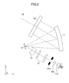
- FIG. 2 is a schematic diagram illustrating an optical path of the optical scanning device 10 (part 1) according to the first embodiment.
- Fig. 3 is another schematic diagram illustrating an optical path of the optical scanning device 10 (part 2) according to the first embodiment.
- Figs. 2 and 3 are drawings of the optical scanning device 10 viewed from different directions. It is to be noted that the below-described optical deflector 16, concave mirror 17, and target scanning surface 18 of Fig. 2 are not illustrated in Fig. 3 for the sake of convenience.
- the optical scanning device 10 mainly includes, for example, light source elements, 11R, 11G, 11B; coupling lenses 12R, 12G, 12B, apertures 13R, 13G, 13B, a compositing element 14, a lens 15, an optical deflector 16, a concave mirror 17, and a target scanning surface 18.
- the light source elements 11R, 11G, 11B, the coupling lenses 12R, 12G, 12B, the compositing element 14, and the lens 15 may be collectively referred to as an incident optical system.
- the optical deflector 16, the concave mirror 17, and the target scanning surface 18 may be collectively referred to as a scanning optical system.
- the light source elements 11R, 11G, 11B can radiate light beams of different wavelengths ⁇ R, ⁇ G, ⁇ B, respectively.
- the wavelength ⁇ R may be, for example, 640 nm
- the wavelength ⁇ G may be, for example, 530 nm
- the wavelength ⁇ B may be, for example, 445 nm.
- a laser, an LED (Light Emitting Diode), or an SHG (Second Harmonic Generation) element may be used as the light source elements 11R, 11G, 11B.
- a control unit controls, for example, the light radiation power, and the light radiation timing of the light source elements 11R, 11G, and 11B.
- the control unit may be mounted inside or outside of the optical scanning device 10.
- the light beams which are emitted from the corresponding light source elements 11R, 11G, 11B in accordance with image signals, are converted to substantially parallel beams or converging beams by corresponding coupling lenses 12R, 11G, 12B.
- the converted beams are incident on the apertures 13R, 13G, and 13G.
- convex-shaped glass lens or plastic lenses may be used as the coupling lenses 12R, 12G, and 12B.
- the apertures 13R, 13G, and 13B function to transform the shapes of the light beams incident on the apertures 13R, 13G, and 13B.
- the apertures 13R, 13G, and 13B may transform the light beams into various shapes (e.g., circular shape, elliptical shape, rectangular shape, quadrate shape) in correspondence with, for example, the angle of divergence (divergence angle) of the light beams.
- the optical scanning device 10 may be configured having a single coupling lens and a single aperture that is shared by the light source elements 11R, 11G, and 11B instead of having plural corresponding coupling lenses and plural corresponding apertures.
- the configuration having plural corresponding coupling lenses and plural corresponding apertures has an advantage of being able to adjust the diameter of the beam spot formed on the target scanning surface 18 while attaining sufficient light-use efficiency regardless of the difference of divergence angles among the light source elements 11 R, 11 G, 11 B.
- the compositing element 14 combines (composites) the optical paths of the transformed light beams that are incident on the compositing element 14.
- the compositing element 14 may be, for example, a dichroic mirror having a plate-like or a prism-like shape.
- the compositing element 15 has a function of combining (compositing) light beams into a single optical path by reflecting the light beams therefrom or transmitting the light beams therethrough in accordance with the wavelength of the light beams.
- the light beams whose optical paths are combined by the compositing element 14 are guided to a reflection surface of the light deflector 16 by the lens 15.
- a single meniscus lens having a concave surface side (a side of the meniscus lens on which the concave surface is formed) facing the optical deflector 16 may be used as the lens 15.
- the lens 15 is described in further detail with reference to Fig. 4 .
- Fig. 4 is a schematic diagram for describing the lens 15 according to an embodiment of the present invention.
- the lens 15 has a first surface 15a and a second surface 15b positioned opposite to the first surface 15b. It is preferable for the light beams 15R and 15B to be radiated from the second surface 15b in a size falling within a reflection surface of the optical deflector 16. That is, it is desired that the lens 15 be able to reduce the size of the light beams 15R, 15B that have traveled through the apertures 13R, 13B and guide the reduced light beams 15R, 15B to the optical deflector 16. Therefore, it is preferable for the first surface 15a of the lens 15 to be a convex surface, so that the light beams 15R, 15B can be converged into light beams having desired light beam diameters, respectively.
- the manner in which the light beam 15R is converged at the first surface 15a is different from the manner in which the light beam 15B is converged at the first surface 15a as illustrated in Fig. 14. That is, the light beam 15R and the light beam 15B are dispersed (refracted) differently at the first surface 15a in a case where the light beam 15R has a long wavelength and the light beam 15B has a short wavelength.
- the lens 15 has a shape other than that of a meniscus lens (e.g., a lens having a convex surface on both sides, or a lens having a flat surface on one side and a convex surface on the other side), the divergence angles of the light beams 15R, 15B transmitted from the lens 15 vary in accordance with the wavelengths of the light beams 15R, 15B.
- a meniscus lens e.g., a lens having a convex surface on both sides, or a lens having a flat surface on one side and a convex surface on the other side
- the lens 15 By using a concave surface of a meniscus lens 15 as the second surface 15b of the lens 15, the light beams 15R, 15B dispersed at the first surface 15a are refracted by the second surface 15b in a manner that the direction of the divergence of the light beams 15R, 15B is returned back to a state before being dispersed at the first surface 15a.
- the lens 15 prevents varying of the divergence of the light beams 15R, 15B transmitted therefrom and guides the light beams 15R, 15B to the optical deflector 16. Thereby, brightness of an image formed by the image forming apparatus 20 can be improved without loss of light quantity of light beams having specific wavelengths.
- the light beam radiated from the incident optical system and guided to the reflection surface of the optical deflector 16 is two-dimensionally deflected by the optical deflector 16.
- the optical deflector 16 may be, for example, a single fine-sized mirror that can oscillate relative to 2 perpendicularly intersecting axes, a single fine-sized mirror that can oscillate relative to a single axis, or a single fine-sized mirror that can rotate in multiple directions.
- the optical deflector 16 may be a MEMS (Micro Electro Mechanical System) mirror manufactured by a semiconductor process.
- the optical deflector 16 may be driven by, for example, an actuator that exerts a driving force generated by deformation force of a piezoelectric element.
- the light beam deflected two-dimensionally by the optical deflector 16 is incident on the concave mirror 17 and reflected by the concave mirror 17. Thereby, a two-dimensional image is formed (depicted) on the target scanning surface 18 by the light beam reflected from the concave mirror 17.
- the optical deflector 16, the concave mirror 17, and the target scanning surface 18 are preferred to be arranged, so that the light beam incident on the target scanning surface 18 has substantially the same orientation as the orientation of the light beam incident to the optical deflector 16.
- the light beam incident on the target scanning surface 18 is substantially orthogonal to the target scanning surface 18, high transmission efficiency can be attained for a large area of the two-dimensional image. Owing to the concave mirror 17 used in the optical scanning device 10, the following effects can be attained.
- the concave mirror 17 has no wavelength dispersion.
- the concave mirror 17 reduces the scanning angle of the light beam incident on the target scanning surface 18.
- the concave mirror 17 can reduce the incident angle of the target scanning surface 18 for all scanning angles on the target scanning surface 18, to thereby increase the brightness of the target scanning surface 18.
- the term "deviation of color(s)" refers to deviation of the position(s) of one or more beam spots formed on the target scanning surface 18 by the light source elements 11R, 11G, 11B having different wavelengths.
- size-reduction of the optical scanning device 10 can be achieved by returning optical paths from the concave mirror 17.
- the rate characteristic of the light beams scanned on the target scanning surface can be corrected.
- the concave mirror 17 provides an isokinetic property to the light beam deflected by the optical deflector 16. Thereby, the pitch of the pixels of the image formed on the target scanning surface 18 can be equalized (consistent pixel pitch).
- a Fresnel lens or a refractive lens it is possible for a Fresnel lens or a refractive lens to be positioned immediately in front of (immediately before) the target scanning surface 18 instead of the concave mirror 17.
- a shadow(s) is formed at a serrate-shaped back cut part of the Fresnel lens and causes undesired loss of light quantity.
- a refractive lens is used instead of the concave mirror 17
- scattering of multiple light beams occurs and causes the multiple light beams to deviate from their intended positions in accordance with wavelength. As a result, an undesired problem of color deviation occurs.
- the target scanning surface 18 is a surface having transparency (transmission) enabling a two-dimensional image to be formed thereon by an incident light beam reflected from the concave mirror 17.
- a diffuser may be used as the target scanning surface 18.
- the diffuser has a function of scattering incident light in a direction in which the incident light travels.
- a micro lens array it is possible for a micro lens array to be used instead of the diffuser.
- the forming of shadows between the lenses of the micro lens array causes a significant loss of light quantity. This results in an undesired problem of decrease of light-use efficiency.
- the diffusion angle of transmitted light can be selected by designing the surface of the diffuser into a predetermined shape. Therefore, it is preferable to use the diffuser as the target scanning surface 17 because the diffuser can reduce loss of light quantity of the light beam that is to be guided to a subsequent optical system. For example, it is possible for the diffuser to diffuse light to the extent (range) necessary while maintaining high transmittance by, for example, randomly forming fine-sized concavities and convexities that are equal to or less than the wavelengths of the light being used on the surface of the diffuser or forming a linear concave-convex shape on the surface of the diffuser.
- Fig. 5 is a schematic diagram for describing the arrangement of the optical deflector 16 and the concave mirror 17 according to an embodiment of the present invention.
- the optical deflector 16 and the concave mirror 17 are arranged, so that the sign of the deflection angle of the optical deflector 16 and the sign of the deflection angle of the concave mirror 17 (i.e. an angle formed by light beams incident on and deflected from the optical deflector 16 and angle formed by light beams incident on and reflected from the concave mirror 17) become opposite to each other (i.e. positive or negative).
- the optical path of the light beam incident on the optical deflector 16, deflected by the deflector 16, and reflected from the concave mirror 17 forms a shape of a letter "Z" when viewing the optical deflector 16 and the concave mirror 17 from a direction (X direction) that is perpendicular to a YZ plane.
- a positive deflection angle is an angle measured in a counter-clockwise direction starting from a direction in which an incident light beam travels
- the sign of a deflection angle 16d of the optical deflector 16 is negative
- the sign of a deflection angle 17d of the concave mirror 17 is positive. Accordingly, the optical deflector 16 and the concave mirror 17 are arranged, so that the signs of the deflection angle 16d of the optical deflector 16 and the deflection angle 17d of the concave mirror 17 become opposite to each other.
- the difference between the optical path of the light beam reaching an upper edge of the target scanning surface 18 and the optical path of the light beam reaching a lower edge of the target scanning surface 18 becomes smaller.
- trapezoidal distortion or bending of an image formed on the target scanning surface 18 can be reduced.
- the optical deflector 16 and the concave mirror 17 are arranged in an optical path of the light beams, so that the sign of the deflection angle 16d of the optical deflector 16 and the sign of the deflection angle 17d of the concave mirror 17 are opposite to each other.
- the concave mirror 17 color deviation of the image formed on the target scanning surface 18 can be reduced. Further, the incidence angle of the target scanning surface 18 can be reduced for all scanning angles. Thereby, the brightness of the target scanning surface 18 can be increased. Further, the difference between the optical path of the light beam reaching an upper edge of the target scanning surface 18 and the optical path of the light beam reaching a lower edge of the target scanning surface 18 becomes smaller by arranging the optical deflector 16 and the concave mirror 17, so that the sign of the deflection angle 16d of the optical deflector 16 and the sign of the deflection angle 17d of the concave mirror 17 are opposite to each other. Therefore, trapezoidal distortion and bending of the image formed on the target scanning surface 18 can be reduced. Further, the size of the optical scanning device 10 can be reduced by using the concave mirror 17. In other words, size-reduction of the optical scanning device 10 can be achieved while ensuring sufficient brightness and high quality of the image formed with the optical scanning device 10.
- first mirror 21, the second mirror 22, and the half mirror 23 are described with reference to Fig. 1 .
- a convex mirror is used as the first mirror 21
- a concave mirror is used as the second mirror 22
- a half mirror having a flat reflection surface is used as the half mirror 23.
- at least one of the first mirror 21 and the second mirror 22 may be a convex mirror.
- the first and the second mirrors 21, 22 may also be collectively referred to as a "projection optical system".
- each of the light beams transmitted through the target scanning surface 18 of the optical scanning device 10 is returned (reflected) by the first mirror 21 and is incident to the second mirror 22. Then, each of the light beams incident on the second mirror is returned (reflected) by the second mirror 22 and is incident on the half mirror 23.
- the first mirror (in this embodiment, convex mirror) 21 is positioned immediately in back of (immediately after) the target scanning surface 18 in the image forming apparatus 20, sunlight that enters into the entire optical system of the image forming apparatus 20 is diffused by the first mirror (convex mirror) 21. Therefore, sunlight entering into the entire optical system of the image forming apparatus 20 can be prevented from concentrating on the target scanning surface 18. Further, the convex surface of the first mirror 21 can widen the angle of view of an intermediate image having a limited (finite) angle of divergence and reduce the length of the entire optical path of the image forming apparatus 20. Therefore, the first mirror 21 is suited for size-reduction of the image forming apparatus 20. The first mirror 21 also has an advantage of preventing chromatic aberration with respect to a lens.
- the half mirror 23 has a transmittance in a visible range of approximately 10%-70%.
- a reflection surface of the half mirror 23 is provided on a side on which the light beam reflected from the second mirror 22 is incident.
- a multilayer dielectric or a wire grid may be formed in the reflection surface of the half mirror 23.
- the reflection surface of the half mirror 23 can selectively reflect wavebands of the light beams radiated from the light source elements 11R, 11G, and 11B. In other words, the reflection surface of the half mirror 23 can increase reflectivity for light beams having a reflection peak including the wavelengths ⁇ R, ⁇ G, ⁇ B, a reflection band including the wavelengths ⁇ R, ⁇ G, ⁇ B or reflectivity with respect to a certain deflection direction.
- the reflection surface of the half mirror 23 is flat whereas a surface of the half mirror 23 opposite to the reflection surface is substantially parallel to the reflection surface. Accordingly, the thickness of the half mirror 23 is substantially uniform.
- the half mirror 23 can selectively reflect wavelength bands of the light beams radiated from the light source elements 11R, 11G, and 11B. Accordingly, brightness of an image formed by radiating multiple light beams of a particular wavelength from the optical scanning device 10 can be increased.
- the reflection surface of the first mirror 21 can be an anamorphic surface. That is, the reflection surface of the first mirror 21 enables a curvature of a predetermined direction to be different from a curvature of a direction orthogonal to the predetermined direction.
- the curved shaped of the reflection surface can be adjusted. Thereby, reflection aberration correction performance of the first mirror 21 can be improved.
- Fig. 6 is a schematic diagram for describing a positional relationship between the target scanning surface 18 and the half mirror 23 according to an embodiment of the present invention.
- the target scanning surface 18 and the half mirror 23 are arranged in the image forming apparatus 20, so that a normal line of the target scanning surface 18 does not intersect the half mirror 23.
- stray light transmitted from the target scanning surface 18 can be prevented from entering the half mirror 23.
- a ghost image can be prevented from being formed in the target scanning surface 18.
- normal lines 18h of the target scanning surface 18 Although only 3 lines are illustrated as normal lines 18h of the target scanning surface 18, the target scanning surface 18 and the half mirror 23 are arranged, so that all of the normal lines (including the 3 normal lines 18h illustrated in Fig. 6 ) of the target scanning surface 18 do not intersect with the half mirror 23.
- Fig. 7 is a schematic diagram for describing a cross section of each of the light beams transmitted through the target scanning surface 18 according to an embodiment of the present invention. It is to be noted that the optical path from the optical deflector 16 to the virtual image 25 is illustrated as a straight line for the sake of convenience.
- the cross section of each of the light beams transmitted through the target scanning surface 18 of the optical scanning device 10 can be formed into an elliptical shape.
- the cross section 18d of each of the light beams diffused by the diffuser can be formed into an elliptical shape.
- the aspect ratio (vertical (Y direction): horizontal (X direction)) of the virtual image 25 is 1:4, it is preferable for the cross section 18d of each of the light beams to be an elliptical shape having a vertical/horizontal ratio of approximately 1:4.
- a diffuser as the target scanning surface 18, forming the cross section of each of the light beams diffused by the diffuser into an elliptical shape, and matching a long axis (major axis) direction of the elliptical shape with a longitudinal direction of the virtual image 25, there can be obtained an optical system having substantially all of the light beams (rays) transmitted from the target scanning surface 18 contribute to forming an image (image formation).
- the optical scanning device 10 In forming an image where the virtual image 25 has a long side in the X direction similar to the target scanning surface 18 having a long side in the X direction, the light-use efficiency in the Y direction is degraded and the image cannot attain high brightness if the cross-section of each of the light beams has, for example, a circular shape.
- the cross section 18d of each of the light beams has an elliptical shape having an vertical/horizontal ratio matching the aspect ratio of the virtual image 25, the optical scanning device 10 according to an embodiment of the present invention is able to improve light-use efficiency in the Y direction and form an image having high brightness.
- the image forming apparatus 20 can be mounted on the vehicle 100 such as an automobile.
- the image forming apparatus 20 may be integrated with a component such as the front window 110 of the vehicle 100.
- the light beam(s) reflected from the reflection surface of the half mirror 23 is incident on the eyeball 24 of the driver in a driver seat of the vehicle 100.
- a two-dimensional image formed on the target scanning surface 18 is visually recognized by the driver as an enlarged (magnified) virtual image 25 at a predetermined position in front of the reflection surface of the half mirror 23 (including a case where the half mirror 23 is integrated with the front window 110 of the vehicle 100).
- the two-dimensional image formed on the target scanning surface 18 may be, for example, measurement data of a measuring instrument of the vehicle 100 or map data.
- the virtual image 25 is viewed at a predetermined position in front of the reflection surface of the half mirror 23 (including a case where the half mirror 23 is integrated with the front window 110 of the vehicle 100), the driver of the vehicle 100 can view, for example, measurement data or map data without having to significantly move his/her focus (viewpoint) in a state looking forward (head-up position).
- a virtual image 25 which is an enlarged (magnified) image of a two-dimensional image formed on the target scanning surface 18 of the optical scanning device 10, can be obtained with the above-described embodiment of the image forming apparatus 20 including the first mirror 21, the second mirror 22, and the half mirror 23. Thereby, a so-called head-up display can be obtained.
- the half mirror 23 is included as a component of the image forming apparatus 20 and an embodiment in which the half mirror 23 is not included as a component of the image forming apparatus 20.
- the front window 110 of the vehicle 100 may be accommodated with a function(s) of the half mirror 23.
- the image forming apparatus 20 With the image forming apparatus 20 according to the above-described first embodiment of the present invention, there can be obtained a projection optical system including the optical scanning device 10 and the convex mirror in which the optical deflector 16 deflects light beams radiated from the light source elements 11R, 11G, 11B two-dimensionally and forms a two-dimensional image on the target scanning surface 18 having a transparent property. Further, the target scanning surface (diffuser) 18 can form the virtual image 25 by enlarging and projecting the two-dimensional image in a predetermined position on a side opposite to the reflection surface of the half mirror 23.
- the optical scanning device 10 included in the image forming apparatus 20
- the optical system can attain high efficiency with little loss of light quantity.
- high brightness can be formed without having to use large-sized light source elements.
- loss of light quantity can be prevented, and images having high brightness can be formed.
- the angle of view can be widened for an intermediate image having a narrow divergence angle by the convex mirror.
- the screen size of the image forming apparatus 20 can be increased and size reduction of the image forming apparatus 20 can be achieved.
- the image forming apparatus 20 can attain high brightness, increase screen size, and achieve size-reduction at the same time.
- a panel type image forming apparatus which does not perform optical scanning (e.g., non-scanning type image forming apparatus such as a liquid crystal panel or a digital light processor)
- optical scanning e.g., non-scanning type image forming apparatus such as a liquid crystal panel or a digital light processor
- the panel-type image forming apparatus would require a strong light source that can illuminate a single screen as a whole.
- the panel-type image forming apparatus requires large heat releasing components such as a heat sink. This prevents size-reduction of the panel-type image forming apparatus.
- the arrangement of optical elements in an optical scanning device is different from that of the optical scanning device 10 of the first embodiment.
- like components are denoted with like reference numerals as those of the first embodiment and are not further described.
- Fig. 8 is a schematic diagram illustrating an optical path of an optical scanning device 10A according to the modified example of the first embodiment. More specifically, Fig. 8 illustrates the optical path of the optical scanning device 10A viewed from the same direction as Fig. 3 . Similar to Fig. 3 , the optical deflector 16, the concave mirror 17, and the target scanning surface 1 are not illustrated in Fig. 8 for the sake of convenience. In the optical scanning device 10A, the arrangement of the optical deflector 16, the concave mirror 17, and the target scanning surface 18 is substantially the same as that of the optical scanning device 10.
- a group including the light source element 11R, the coupling lens 12R, and the aperture 13R, a group including the light source element 11G, the coupling lens 12G, and the aperture 13G, and a group including the light source element 11B, the coupling lens 12B, and the aperture 13B are arranged substantially parallel to a direction in which each corresponding light beam travels.
- the light beams formed (shaped) by the aperture 13R, 13G, and 13B are incident on the compositing element 14 and have their optical paths composited (combined) by the compositing element 14. Further, the optical system including the compositing element 14 and optical devices positioned after the compositing element 14 operate in a similar manner as those of the optical scanning device 10.
- the arrangement of optical devices such as the light source element, the coupling lens, the aperture, and the compositing element can be discretionarily decided.
- the optical scanning device 10A may be used instead of the optical scanning device 10.
- first-third examples of the first embodiment of the present invention are described. More specifically, the first-third examples of the first embodiment of the present invention are design examples of the first mirror 21, the second mirror 22, and the half mirror 23.
- Fig. 9 is a schematic diagram illustrating an optical system according to the first example. As illustrated in Fig. 9 , a convex mirror is used as the first mirror 21, a concave mirror is used as the second mirror 22, and a half mirror having a flat reflection surface is used as the half mirror 23 in the first example.
- the first mirror 21 increases the radiation angle of the incident light beams. Thereby, the length of the optical paths in the image forming apparatus can be shortened.
- a final power surface is to have enough power to converge multiple light beams.
- the half mirror 23 of the first example has a flat surface, a concave mirror is to be used as the second mirror 22, so that the entire projection optical system can have a positive power.
- the projection optical system can be formed having a depth (lateral direction in Fig. 9 ) that is substantially close to an effective diameter of the half mirror 23.
- the position (image plane position) of the virtual image 25 is 2 m apart from the eyeball 24 of the driver. Further, in the first example, the angle of view (surface angle view) of the virtual image 25 is 12 ⁇ 3 deg.
- Fig. 10 is a schematic diagram illustrating an optical system according to the second example.
- a convex mirror is used as the first mirror 21
- a flat mirror is used as the second mirror 22
- a half mirror having a concave reflection surface is used as the half mirror in the second example.
- the reflection surface of the half mirror 23 is a concave surface
- a surface of the half mirror 23 opposite to the reflection surface is substantially parallel to the reflection surface.
- the thickness of the half mirror 23 is substantially uniform.
- the convex surface of the first mirror 21 is an anamorphic surface in which a curvature of a predetermined direction is different from a curvature of a direction orthogonal to the predetermined direction.
- an anamorphic surface as the reflection surface of the first mirror 21
- the curved shaped of the convex surface of the first mirror 21 can be adjusted. Thereby, reflection aberration correction performance of the first mirror 21 can be improved.
- Fig. 11 is a schematic diagram illustrating the half mirror 23 of the second example.
- the position of a vertex (deepest point) of the concave surface of the half mirror 23 is deviated approximately a few tens of mm toward the projection optical system with respect to the position of an optical center 23b of the concave surface of the half mirror 23.
- optical center 23b refers to a geometric center of an entire range 23a of the half mirror 23 that is viewable by an observer (e.g., driver of the vehicle 100).
- the deepest point 23c is a deepest recessed part of the entire range 23a of the half mirror 23 that is viewable by the observer.
- the surface of the half mirror 23 toward the observer is an eccentric surface.
- balance can be obtained between an optical path of a light beam incident from the second mirror 22 on a part of the half mirror 23 closer to the second mirror 22 and an optical path of a light beam incident from the second mirror 22 on a part of the half mirror 23 farther away from the second mirror 22.
- distortion generated in the image forming apparatus 20 can be reduced.
- the optical system including the first mirror 21, the second mirror 22, and the half mirror 23 as a whole has a positive power.
- the position (image plane position) of the virtual image 25 is 2 m apart from the eyeball 24 of the driver. Further, in the second example, the angle of view (surface angle view) of the virtual image 25 is 6 ⁇ 2 deg.
- Fig. 12 is a schematic diagram illustrating an optical system according to the third example.
- a concave mirror is used as the first mirror 21
- a convex mirror is used as the second mirror 22
- a half mirror having a concave reflection surface is used as the half mirror 23 in the third example.
- the reflection surface of the half mirror 23 is a concave surface
- a surface of the half mirror 23 opposite to the reflection surface is substantially parallel to the reflection surface.
- the thickness of the half mirror 23 is substantially uniform.
- the radiation angle of the target scanning surface 18 is 10.5 degrees in the X direction and 3.5 degrees in the Y direction.
- the scanning optical system is designed to match the radiation angle of the target scanning surface 18.
- the concave surface of the first mirror 21 is an anamorphic surface in which a curvature of a predetermined direction is different from a curvature of a direction orthogonal to the predetermined direction.
- the radiation angle of the target scanning surface 18 of the third example is designed to be wider compared to those of the first and the second examples. Accordingly, the length of the optical path from the target scanning surface 18 to the half mirror 23 can be shortened. Further, the length from the target scanning surface 18 to the half mirror 23 with respect to the height direction (vertical direction in Fig. 12 ) and the depth direction (horizontal direction in Fig. 12 ) can be less than or equal to the size of the half mirror 23, respectively.
- the position (image plane position) of the virtual image 25 is 2 m apart from the eyeball 24 of the driver. Further, in the third example, the angle of view (surface angle view) of the virtual image 25 is 6 ⁇ 2 deg.
- a single color image may be used by using a single light source element.
- the compositing element 14 is omitted.
- the image forming apparatus 20 may also be mounted on other vehicles such as an airplane or a train.
Abstract
Description
- The present invention relates to an image forming apparatus and a vehicle on which the image forming apparatus is mounted; for example, an image forming apparatus including an optical scanning device for forming a two-dimensional image by scanning a light beam from an optical element, and a vehicle on which such image forming apparatus is mounted.
- In recent years, there has been widely proposed an optical scanning device that forms a two-dimensional image by irradiating multicolor light beams to a mirror that can scan in two-dimensional directions. Particularly, with an optical scanning device using a semiconductor laser as a light source, high light-use efficiency can be attained owing to the high directivity of a light beam irradiated from the semiconductor laser. Further, with the optical scanning device using a semiconductor laser, strong light can be generated inside the optical scanning device without requiring a large heat radiator such as a xenon lamp. In addition, owing to the high directivity of the optical scanning device using a semiconductor laser, a bright image can be formed even with a small size optical system.
- An image forming apparatus such as a head-up display can be manufactured by using the optical scanning device using a semiconductor laser. Because such image forming apparatus is installed in, for example, a vehicle such as an automobile, the image forming apparatus is to be formed in a small size.
- However, by pursing size-reduction of the image forming apparatus, there are problems such as being unable to attain brightness or being unable to provide a large size screen.
- Patent Document 1: Japanese Laid-Open Patent Publication No.
2010-145745 - Patent Document 2: Japanese Laid-Open Patent Publication No.
2010-145746 - The present invention may provide an image forming apparatus and a vehicle on which an image forming apparatus is mounted that substantially obviate one or more of the problems caused by the limitations and disadvantages of the related art.
- Features and advantages of the present invention are set forth in the description which follows, and in part will become apparent from the description and the accompanying drawings, or may be learned by practice of the invention according to the teachings provided in the description. Objects as well as other features and advantages of the present invention will be realized and attained by an image forming apparatus and a vehicle on which an image forming apparatus is mounted particularly pointed out in the specification in such full, clear, concise, and exact terms as to enable a person having ordinary skill in the art to practice the invention.
- To achieve these and other advantages and in accordance with the purpose of the invention, as embodied and broadly described herein, an embodiment of the present invention provides an image forming apparatus including an optical scanning device including a light source element configured to radiate a light beam, an optical deflector configured to deflect the light beam two-dimensionally, and a target scanning surface that is transparent and having a two-dimensional image formed thereon by the light beam deflected from the optical deflector, and a projection optical system including a convex mirror and configured to enlarge and project the two-dimensional image on a target projection surface, wherein the target projection surface includes a reflection surface of a half mirror, wherein the half mirror is positioned outside of the image forming apparatus and configured to transmit a part of a light incident on the half mirror and reflect another part of the light incident on the half mirror.
- Other objects, features and advantages of the present invention will become more apparent from the following detailed description when read in conjunction with the accompanying drawings.
-
-
Fig. 1 is a schematic diagram illustrating an image forming apparatus according to a first embodiment of the present invention; -
Fig. 2 is a schematic diagram illustrating an optical path of an optical scanning device according to the first embodiment of the present invention (part 1); -
Fig. 3 is a schematic diagram illustrating an optical path of an optical scanning device according to the first embodiment of the present invention (part 2); -
Fig. 4 is a schematic diagram for describing a lens according to an embodiment of the present invention; -
Fig. 5 is a schematic diagram for describing an arrangement of an optical deflector and a concave mirror according to an embodiment of the present invention; -
Fig. 6 is a schematic diagram for describing a positional relationship between a target scan surface and a half mirror according to an embodiment of the present invention; -
Fig. 7 is a schematic diagram for describing a cross section of each light beam transmitted through a target scan surface according to an embodiment of the present invention; -
Fig. 8 is a schematic diagram illustrating an optical path of an optical scanning device according to a modified example of the first embodiment of the present invention; -
Fig. 9 is a schematic diagram illustrating an optical system according to an embodiment of the present invention; -
Fig. 10 is a schematic diagram illustrating an optical system according to another embodiment of the present invention; -
Fig. 11 is a schematic diagram illustrating a half mirror according to another embodiment of the present invention; and -
Fig. 12 is schematic diagram illustrating an optical system according to another embodiment of the present invention. -
Fig. 1 is a schematic diagram illustrating animage forming apparatus 20 according to a first embodiment of the present invention. With reference toFig. 1 , theimage forming apparatus 20 mainly includes, for example, anoptical scanning device 10, afirst mirror 21, asecond mirror 22, and ahalf mirror 23. As described below, thehalf mirror 23 may be omitted from theimage forming apparatus 20. InFig. 1 ,reference numeral 24 indicates an eyeball of an observer that observes an image formed by the image forming apparatus 20 (hereinafter also referred to as "eyeball 24") andreference numeral 25 indicates a virtual image (hereinafter also referred to as "virtual image 25"). Further,reference numeral 100 indicates a vehicle on which theimage forming apparatus 20 is mounted (hereinafter also referred to as "vehicle 100") andreference numeral 110 indicates a front window of the vehicle 100 (hereinafter also referred to as "front window 110"). - First, the
optical scanning device 10 according to an embodiment of the present invention is described.Fig. 2 is a schematic diagram illustrating an optical path of the optical scanning device 10 (part 1) according to the first embodiment.Fig. 3 is another schematic diagram illustrating an optical path of the optical scanning device 10 (part 2) according to the first embodiment.Figs. 2 and3 are drawings of theoptical scanning device 10 viewed from different directions. It is to be noted that the below-describedoptical deflector 16,concave mirror 17, andtarget scanning surface 18 ofFig. 2 are not illustrated inFig. 3 for the sake of convenience. - With reference to
Figs. 2 and3 , theoptical scanning device 10 mainly includes, for example, light source elements, 11R, 11G, 11B;coupling lenses apertures element 14, alens 15, anoptical deflector 16, aconcave mirror 17, and atarget scanning surface 18. - It is to be noted that the
light source elements coupling lenses element 14, and thelens 15 may be collectively referred to as an incident optical system. Further, theoptical deflector 16, theconcave mirror 17, and thetarget scanning surface 18 may be collectively referred to as a scanning optical system. - In the
optical scanning device 10, thelight source elements light source elements - From a standpoint of achieving size reduction while ensuring brightness and high image quality, it is preferable to use a semiconductor laser for each of the
light source elements light source elements optical scanning device 10. - The light beams, which are emitted from the corresponding
light source elements corresponding coupling lenses apertures coupling lenses - The
apertures apertures apertures - Alternatively, the
optical scanning device 10 may be configured having a single coupling lens and a single aperture that is shared by thelight source elements target scanning surface 18 while attaining sufficient light-use efficiency regardless of the difference of divergence angles among thelight source elements - The light beams, which are transformed (shaped) by the
apertures element 14. The compositingelement 14 combines (composites) the optical paths of the transformed light beams that are incident on the compositingelement 14. The compositingelement 14 may be, for example, a dichroic mirror having a plate-like or a prism-like shape. The compositingelement 15 has a function of combining (compositing) light beams into a single optical path by reflecting the light beams therefrom or transmitting the light beams therethrough in accordance with the wavelength of the light beams. - The light beams whose optical paths are combined by the compositing
element 14 are guided to a reflection surface of thelight deflector 16 by thelens 15. For example, a single meniscus lens having a concave surface side (a side of the meniscus lens on which the concave surface is formed) facing theoptical deflector 16 may be used as thelens 15. Next, thelens 15 is described in further detail with reference toFig. 4 . -
Fig. 4 is a schematic diagram for describing thelens 15 according to an embodiment of the present invention. InFig. 4 , twolight beams lens 15. Thelens 15 has afirst surface 15a and asecond surface 15b positioned opposite to thefirst surface 15b. It is preferable for thelight beams second surface 15b in a size falling within a reflection surface of theoptical deflector 16. That is, it is desired that thelens 15 be able to reduce the size of thelight beams apertures light beams optical deflector 16. Therefore, it is preferable for thefirst surface 15a of thelens 15 to be a convex surface, so that thelight beams - In a case where the
light beam 15R has a long wave length and thelight beam 15B has a short wavelength, the manner in which thelight beam 15R is converged at thefirst surface 15a is different from the manner in which thelight beam 15B is converged at thefirst surface 15a as illustrated in Fig. 14. That is, thelight beam 15R and thelight beam 15B are dispersed (refracted) differently at thefirst surface 15a in a case where thelight beam 15R has a long wavelength and thelight beam 15B has a short wavelength. In a case where thelens 15 has a shape other than that of a meniscus lens (e.g., a lens having a convex surface on both sides, or a lens having a flat surface on one side and a convex surface on the other side), the divergence angles of thelight beams lens 15 vary in accordance with the wavelengths of thelight beams - By using a concave surface of a
meniscus lens 15 as thesecond surface 15b of thelens 15, thelight beams first surface 15a are refracted by thesecond surface 15b in a manner that the direction of the divergence of thelight beams first surface 15a. As a result, in a case where thelight beams lens 15, thelens 15 prevents varying of the divergence of thelight beams light beams optical deflector 16. Thereby, brightness of an image formed by theimage forming apparatus 20 can be improved without loss of light quantity of light beams having specific wavelengths. - Returning to
Figs. 2 and3 , the light beam radiated from the incident optical system and guided to the reflection surface of theoptical deflector 16 is two-dimensionally deflected by theoptical deflector 16. Theoptical deflector 16 may be, for example, a single fine-sized mirror that can oscillate relative to 2 perpendicularly intersecting axes, a single fine-sized mirror that can oscillate relative to a single axis, or a single fine-sized mirror that can rotate in multiple directions. For example, theoptical deflector 16 may be a MEMS (Micro Electro Mechanical System) mirror manufactured by a semiconductor process. Theoptical deflector 16 may be driven by, for example, an actuator that exerts a driving force generated by deformation force of a piezoelectric element. - The light beam deflected two-dimensionally by the
optical deflector 16 is incident on theconcave mirror 17 and reflected by theconcave mirror 17. Thereby, a two-dimensional image is formed (depicted) on thetarget scanning surface 18 by the light beam reflected from theconcave mirror 17. Theoptical deflector 16, theconcave mirror 17, and thetarget scanning surface 18 are preferred to be arranged, so that the light beam incident on thetarget scanning surface 18 has substantially the same orientation as the orientation of the light beam incident to theoptical deflector 16. By such arrangement of theoptical deflector 16, theconcave mirror 17, and thetarget scanning surface 18, distortion of the two-dimensional image formed on thetarget scanning surface 18 can be reduced. Because the light beam incident on thetarget scanning surface 18 is substantially orthogonal to thetarget scanning surface 18, high transmission efficiency can be attained for a large area of the two-dimensional image. Owing to theconcave mirror 17 used in theoptical scanning device 10, the following effects can be attained. - As the first effect, deviation of a color(s) of the image formed on the
target scanning surface 18 can be prevented because theconcave mirror 17 has no wavelength dispersion. As the second effect, deviation of a color(s) of the image formed on thetarget scanning surface 18 can also be prevented because theconcave mirror 17 reduces the scanning angle of the light beam incident on thetarget scanning surface 18. As the third effect, theconcave mirror 17 can reduce the incident angle of thetarget scanning surface 18 for all scanning angles on thetarget scanning surface 18, to thereby increase the brightness of thetarget scanning surface 18. In this embodiment, the term "deviation of color(s)" refers to deviation of the position(s) of one or more beam spots formed on thetarget scanning surface 18 by thelight source elements optical scanning device 10 can be achieved by returning optical paths from theconcave mirror 17. - Because at least one side of the surface of the
concave mirror 17 does not have an arcuate shape, the rate characteristic of the light beams scanned on the target scanning surface can be corrected. In other words, theconcave mirror 17 provides an isokinetic property to the light beam deflected by theoptical deflector 16. Thereby, the pitch of the pixels of the image formed on thetarget scanning surface 18 can be equalized (consistent pixel pitch). - It is possible for a Fresnel lens or a refractive lens to be positioned immediately in front of (immediately before) the
target scanning surface 18 instead of theconcave mirror 17. However, in a case where a Fresnel lens is used instead of theconcave mirror 17, a shadow(s) is formed at a serrate-shaped back cut part of the Fresnel lens and causes undesired loss of light quantity. Further, in a case where a refractive lens is used instead of theconcave mirror 17, scattering of multiple light beams occurs and causes the multiple light beams to deviate from their intended positions in accordance with wavelength. As a result, an undesired problem of color deviation occurs. - The
target scanning surface 18 is a surface having transparency (transmission) enabling a two-dimensional image to be formed thereon by an incident light beam reflected from theconcave mirror 17. For example, a diffuser may be used as thetarget scanning surface 18. The diffuser has a function of scattering incident light in a direction in which the incident light travels. It is possible for a micro lens array to be used instead of the diffuser. However, in a case of using a micro lens array, the forming of shadows between the lenses of the micro lens array causes a significant loss of light quantity. This results in an undesired problem of decrease of light-use efficiency. - On the other hand, the diffusion angle of transmitted light can be selected by designing the surface of the diffuser into a predetermined shape. Therefore, it is preferable to use the diffuser as the
target scanning surface 17 because the diffuser can reduce loss of light quantity of the light beam that is to be guided to a subsequent optical system. For example, it is possible for the diffuser to diffuse light to the extent (range) necessary while maintaining high transmittance by, for example, randomly forming fine-sized concavities and convexities that are equal to or less than the wavelengths of the light being used on the surface of the diffuser or forming a linear concave-convex shape on the surface of the diffuser. - Next, the arrangement of the
optical deflector 16 and theconcave mirror 17 according to an embodiment of the present invention is described with reference toFig. 5. Fig. 5 is a schematic diagram for describing the arrangement of theoptical deflector 16 and theconcave mirror 17 according to an embodiment of the present invention. InFig. 5 , theoptical deflector 16 and theconcave mirror 17 are arranged, so that the sign of the deflection angle of theoptical deflector 16 and the sign of the deflection angle of the concave mirror 17 (i.e. an angle formed by light beams incident on and deflected from theoptical deflector 16 and angle formed by light beams incident on and reflected from the concave mirror 17) become opposite to each other (i.e. positive or negative). The optical path of the light beam incident on theoptical deflector 16, deflected by thedeflector 16, and reflected from theconcave mirror 17 forms a shape of a letter "Z" when viewing theoptical deflector 16 and theconcave mirror 17 from a direction (X direction) that is perpendicular to a YZ plane. - In the YZ plane, assuming that a positive deflection angle is an angle measured in a counter-clockwise direction starting from a direction in which an incident light beam travels, the sign of a
deflection angle 16d of theoptical deflector 16 is negative, and the sign of adeflection angle 17d of theconcave mirror 17 is positive. Accordingly, theoptical deflector 16 and theconcave mirror 17 are arranged, so that the signs of thedeflection angle 16d of theoptical deflector 16 and thedeflection angle 17d of theconcave mirror 17 become opposite to each other. Owing to this arrangement of theoptical deflector 16 and theconcave mirror 17, the difference between the optical path of the light beam reaching an upper edge of thetarget scanning surface 18 and the optical path of the light beam reaching a lower edge of thetarget scanning surface 18 becomes smaller. As a result, trapezoidal distortion or bending of an image formed on thetarget scanning surface 18 can be reduced. - In a case where trapezoidal distortion or bending of an image occurs when the above-described arrangement of the
optical deflector 16 and theconcave mirror 17 is not used, it is possible to electrically correct the trapezoidal distortion or bending. Even if the trapezoidal distortion or bending is corrected, the image becomes dark owing to invalid pixels generated by the correction. In contrast, sufficient brightness and high quality can be attained with theimage forming apparatus 20 using theoptical scanning device 10 because trapezoidal distortion and bending can be reduced without performing electrical correction. - Thus, in the above-described embodiment of the present invention where a multicolor image is formed on the
target scanning surface 18 by scanning light beams of different wavelengths radiated from thelight source elements optical deflector 16 and theconcave mirror 17 are arranged in an optical path of the light beams, so that the sign of thedeflection angle 16d of theoptical deflector 16 and the sign of thedeflection angle 17d of theconcave mirror 17 are opposite to each other. By such arrangement of theoptical deflector 16 and theconcave mirror 17, the following effects can be attained. - That is, by using the
concave mirror 17, color deviation of the image formed on thetarget scanning surface 18 can be reduced. Further, the incidence angle of thetarget scanning surface 18 can be reduced for all scanning angles. Thereby, the brightness of thetarget scanning surface 18 can be increased. Further, the difference between the optical path of the light beam reaching an upper edge of thetarget scanning surface 18 and the optical path of the light beam reaching a lower edge of thetarget scanning surface 18 becomes smaller by arranging theoptical deflector 16 and theconcave mirror 17, so that the sign of thedeflection angle 16d of theoptical deflector 16 and the sign of thedeflection angle 17d of theconcave mirror 17 are opposite to each other. Therefore, trapezoidal distortion and bending of the image formed on thetarget scanning surface 18 can be reduced. Further, the size of theoptical scanning device 10 can be reduced by using theconcave mirror 17. In other words, size-reduction of theoptical scanning device 10 can be achieved while ensuring sufficient brightness and high quality of the image formed with theoptical scanning device 10. - Next, the
first mirror 21, thesecond mirror 22, and thehalf mirror 23 are described with reference toFig. 1 . In the first embodiment of the present invention, a convex mirror is used as thefirst mirror 21, a concave mirror is used as thesecond mirror 22, and a half mirror having a flat reflection surface is used as thehalf mirror 23. In the below-described Examples 1-3 of the present invention, at least one of thefirst mirror 21 and thesecond mirror 22 may be a convex mirror. It is to be noted that the first and the second mirrors 21, 22 may also be collectively referred to as a "projection optical system". - In the
image forming apparatus 20, each of the light beams transmitted through thetarget scanning surface 18 of theoptical scanning device 10 is returned (reflected) by thefirst mirror 21 and is incident to thesecond mirror 22. Then, each of the light beams incident on the second mirror is returned (reflected) by thesecond mirror 22 and is incident on thehalf mirror 23. - Because the first mirror (in this embodiment, convex mirror) 21 is positioned immediately in back of (immediately after) the
target scanning surface 18 in theimage forming apparatus 20, sunlight that enters into the entire optical system of theimage forming apparatus 20 is diffused by the first mirror (convex mirror) 21. Therefore, sunlight entering into the entire optical system of theimage forming apparatus 20 can be prevented from concentrating on thetarget scanning surface 18. Further, the convex surface of thefirst mirror 21 can widen the angle of view of an intermediate image having a limited (finite) angle of divergence and reduce the length of the entire optical path of theimage forming apparatus 20. Therefore, thefirst mirror 21 is suited for size-reduction of theimage forming apparatus 20. Thefirst mirror 21 also has an advantage of preventing chromatic aberration with respect to a lens. - The
half mirror 23 has a transmittance in a visible range of approximately 10%-70%. A reflection surface of thehalf mirror 23 is provided on a side on which the light beam reflected from thesecond mirror 22 is incident. For example, a multilayer dielectric or a wire grid may be formed in the reflection surface of thehalf mirror 23. The reflection surface of thehalf mirror 23 can selectively reflect wavebands of the light beams radiated from thelight source elements half mirror 23 can increase reflectivity for light beams having a reflection peak including the wavelengths λR, λG, λB, a reflection band including the wavelengths λR, λG, λB or reflectivity with respect to a certain deflection direction. - In the first embodiment, the reflection surface of the
half mirror 23 is flat whereas a surface of thehalf mirror 23 opposite to the reflection surface is substantially parallel to the reflection surface. Accordingly, the thickness of thehalf mirror 23 is substantially uniform. - In other words, the
half mirror 23 can selectively reflect wavelength bands of the light beams radiated from thelight source elements optical scanning device 10 can be increased. - It is to be noted that the reflection surface of the
first mirror 21 can be an anamorphic surface. That is, the reflection surface of thefirst mirror 21 enables a curvature of a predetermined direction to be different from a curvature of a direction orthogonal to the predetermined direction. By using an anamorphic surface as the reflection surface of thefirst mirror 21, the curved shaped of the reflection surface can be adjusted. Thereby, reflection aberration correction performance of thefirst mirror 21 can be improved. -
Fig. 6 is a schematic diagram for describing a positional relationship between thetarget scanning surface 18 and thehalf mirror 23 according to an embodiment of the present invention. As illustrated inFig. 6 , thetarget scanning surface 18 and thehalf mirror 23 are arranged in theimage forming apparatus 20, so that a normal line of thetarget scanning surface 18 does not intersect thehalf mirror 23. By arranging thetarget scanning surface 18 and thehalf mirror 23 in this manner, stray light transmitted from thetarget scanning surface 18 can be prevented from entering thehalf mirror 23. Thereby, a ghost image can be prevented from being formed in thetarget scanning surface 18. - Although only 3 lines are illustrated as
normal lines 18h of thetarget scanning surface 18, thetarget scanning surface 18 and thehalf mirror 23 are arranged, so that all of the normal lines (including the 3normal lines 18h illustrated inFig. 6 ) of thetarget scanning surface 18 do not intersect with thehalf mirror 23. - Next, the shape of a cross section of each of the light beams transmitted through the
target scanning surface 18 of theoptical scanning device 10 is described with reference toFig. 7. Fig. 7 is a schematic diagram for describing a cross section of each of the light beams transmitted through thetarget scanning surface 18 according to an embodiment of the present invention. It is to be noted that the optical path from theoptical deflector 16 to thevirtual image 25 is illustrated as a straight line for the sake of convenience. - As illustrated in
Fig. 7 , the cross section of each of the light beams transmitted through thetarget scanning surface 18 of theoptical scanning device 10 can be formed into an elliptical shape. In other words, by using a diffuser as thetarget scanning surface 18, thecross section 18d of each of the light beams diffused by the diffuser can be formed into an elliptical shape. In a case where the aspect ratio (vertical (Y direction): horizontal (X direction)) of thevirtual image 25 is 1:4, it is preferable for thecross section 18d of each of the light beams to be an elliptical shape having a vertical/horizontal ratio of approximately 1:4. - Accordingly, by using a diffuser as the
target scanning surface 18, forming the cross section of each of the light beams diffused by the diffuser into an elliptical shape, and matching a long axis (major axis) direction of the elliptical shape with a longitudinal direction of thevirtual image 25, there can be obtained an optical system having substantially all of the light beams (rays) transmitted from thetarget scanning surface 18 contribute to forming an image (image formation). - In forming an image where the
virtual image 25 has a long side in the X direction similar to thetarget scanning surface 18 having a long side in the X direction, the light-use efficiency in the Y direction is degraded and the image cannot attain high brightness if the cross-section of each of the light beams has, for example, a circular shape. In contrast, because thecross section 18d of each of the light beams has an elliptical shape having an vertical/horizontal ratio matching the aspect ratio of thevirtual image 25, theoptical scanning device 10 according to an embodiment of the present invention is able to improve light-use efficiency in the Y direction and form an image having high brightness. - The
image forming apparatus 20 according to an embodiment of the present invention can be mounted on thevehicle 100 such as an automobile. In such case of mounting theimage forming apparatus 20 on thevehicle 100, theimage forming apparatus 20 may be integrated with a component such as thefront window 110 of thevehicle 100. By mounting theimage forming apparatus 20 on thevehicle 100 in a position in front of a driver of thevehicle 100, the light beam(s) reflected from the reflection surface of the half mirror 23 (including a case where thehalf mirror 23 is integrated with thefront window 110 of the vehicle 100) is incident on theeyeball 24 of the driver in a driver seat of thevehicle 100. Thereby, a two-dimensional image formed on thetarget scanning surface 18 is visually recognized by the driver as an enlarged (magnified)virtual image 25 at a predetermined position in front of the reflection surface of the half mirror 23 (including a case where thehalf mirror 23 is integrated with thefront window 110 of the vehicle 100). - Hence, a so-called head-up display (HUD) can be realized by using the
image forming apparatus 20 according to the above-described embodiment of the present invention. In a case where theimage forming apparatus 20 is used for a head-up display, the two-dimensional image formed on thetarget scanning surface 18 may be, for example, measurement data of a measuring instrument of thevehicle 100 or map data. Because thevirtual image 25 is viewed at a predetermined position in front of the reflection surface of the half mirror 23 (including a case where thehalf mirror 23 is integrated with thefront window 110 of the vehicle 100), the driver of thevehicle 100 can view, for example, measurement data or map data without having to significantly move his/her focus (viewpoint) in a state looking forward (head-up position). - Accordingly, a
virtual image 25, which is an enlarged (magnified) image of a two-dimensional image formed on thetarget scanning surface 18 of theoptical scanning device 10, can be obtained with the above-described embodiment of theimage forming apparatus 20 including thefirst mirror 21, thesecond mirror 22, and thehalf mirror 23. Thereby, a so-called head-up display can be obtained. - According to the description above, there may be an embodiment in which the
half mirror 23 is included as a component of theimage forming apparatus 20 and an embodiment in which thehalf mirror 23 is not included as a component of theimage forming apparatus 20. In the embodiment where thehalf mirror 23 is not included as a component of theimage forming apparatus 20, thefront window 110 of thevehicle 100 may be accommodated with a function(s) of thehalf mirror 23. - With the
image forming apparatus 20 according to the above-described first embodiment of the present invention, there can be obtained a projection optical system including theoptical scanning device 10 and the convex mirror in which theoptical deflector 16 deflects light beams radiated from thelight source elements target scanning surface 18 having a transparent property. Further, the target scanning surface (diffuser) 18 can form thevirtual image 25 by enlarging and projecting the two-dimensional image in a predetermined position on a side opposite to the reflection surface of thehalf mirror 23. - By having the
optical scanning device 10 included in theimage forming apparatus 20, it becomes possible to set the angle of divergence of an image to be formed (including an intermediate image). Moreover, it becomes easier to control the angle of divergence of the intermediate image. Thereby, in an optical system including optical devices including theoptical deflector 16 and those positioned after theoptical deflector 16, the optical system can attain high efficiency with little loss of light quantity. As a result of obtaining a highly efficient optical system, high brightness can be formed without having to use large-sized light source elements. In other words, by being able to set the angle of divergence of thetarget scanning surface 18 to a desired value, loss of light quantity can be prevented, and images having high brightness can be formed. - By providing a projection optical system including a convex mirror in the
image forming apparatus 20, in a case where scanning is performed using a semiconductor laser as an light source element, the angle of view can be widened for an intermediate image having a narrow divergence angle by the convex mirror. Thereby, the screen size of theimage forming apparatus 20 can be increased and size reduction of theimage forming apparatus 20 can be achieved. - That is, by providing a projection optical system including the above-described
optical scanning device 10 and the convex mirror, theimage forming apparatus 20 can attain high brightness, increase screen size, and achieve size-reduction at the same time. - In a case of a panel type image forming apparatus which does not perform optical scanning (e.g., non-scanning type image forming apparatus such as a liquid crystal panel or a digital light processor), it is difficult to attain high brightness, increase screen size, and achieve size-reduction at the same time. This is due to the difficulty of preventing loss of light quantity by controlling the divergence angle of the light from the intermediate image. Further, in order to attain high brightness for a panel-type image forming apparatus, the panel-type image forming apparatus would require a strong light source that can illuminate a single screen as a whole. Thus, the panel-type image forming apparatus requires large heat releasing components such as a heat sink. This prevents size-reduction of the panel-type image forming apparatus.
- In the modified example of the first embodiment, the arrangement of optical elements in an optical scanning device is different from that of the
optical scanning device 10 of the first embodiment. In the modified example of the first embodiment, like components are denoted with like reference numerals as those of the first embodiment and are not further described. -
Fig. 8 is a schematic diagram illustrating an optical path of anoptical scanning device 10A according to the modified example of the first embodiment. More specifically,Fig. 8 illustrates the optical path of theoptical scanning device 10A viewed from the same direction asFig. 3 . Similar toFig. 3 , theoptical deflector 16, theconcave mirror 17, and thetarget scanning surface 1 are not illustrated inFig. 8 for the sake of convenience. In theoptical scanning device 10A, the arrangement of theoptical deflector 16, theconcave mirror 17, and thetarget scanning surface 18 is substantially the same as that of theoptical scanning device 10. - In the
optical scanning device 10A illustrated inFig. 8 , a group including thelight source element 11R, thecoupling lens 12R, and theaperture 13R, a group including thelight source element 11G, thecoupling lens 12G, and theaperture 13G, and a group including thelight source element 11B, thecoupling lens 12B, and theaperture 13B are arranged substantially parallel to a direction in which each corresponding light beam travels. - Similar to the
optical scanning device 10, the light beams formed (shaped) by theaperture compositing element 14 and have their optical paths composited (combined) by thecompositing element 14. Further, the optical system including thecompositing element 14 and optical devices positioned after thecompositing element 14 operate in a similar manner as those of theoptical scanning device 10. - Accordingly, the arrangement of optical devices such as the light source element, the coupling lens, the aperture, and the compositing element can be discretionarily decided. Thus, in the
image forming apparatus 20 according to the modified example, theoptical scanning device 10A may be used instead of theoptical scanning device 10. - Next, first-third examples of the first embodiment of the present invention are described. More specifically, the first-third examples of the first embodiment of the present invention are design examples of the
first mirror 21, thesecond mirror 22, and thehalf mirror 23. -
Fig. 9 is a schematic diagram illustrating an optical system according to the first example. As illustrated inFig. 9 , a convex mirror is used as thefirst mirror 21, a concave mirror is used as thesecond mirror 22, and a half mirror having a flat reflection surface is used as thehalf mirror 23 in the first example. - In the first example, although the light beams transmitted from the
target scanning surface 18 are incident on the first mirror (convex mirror) 21, thefirst mirror 21 increases the radiation angle of the incident light beams. Thereby, the length of the optical paths in the image forming apparatus can be shortened. - In order to allow a driver of the
vehicle 100 to view the enlargedvirtual image 25, a final power surface is to have enough power to converge multiple light beams. Because thehalf mirror 23 of the first example has a flat surface, a concave mirror is to be used as thesecond mirror 22, so that the entire projection optical system can have a positive power. With the configuration of the first example, the projection optical system can be formed having a depth (lateral direction inFig. 9 ) that is substantially close to an effective diameter of thehalf mirror 23. - Next, optical data of the first example are illustrated in Tables 1-3.
[Table 1] FIRST MIRROR 21SECOND MIRROR 22HALF MIRROR 23SURFACE SHAPE CONVEX SHAPE CONCAVE SHAPE FLAT SHAPE CURVATURE RADIUS 156mm 270mm INFINITE INCIDENT ANGLE -31 DEGREES 20 DEGREES 24 DEGREES [Table 2] TARGET SCANNING SURFACE 18FIRST MIRROR 21SECOND MIRROR 22~FIRST MIRROR 21 -SECOND MIRROR 22 - HALF MIRROR 23SURFACE INTERVAL 65mm 80mm 120mm [Table 3] TARGET SCANNING SURFACE 18RADIATION ANGLE OF TARGET SCANNING SURFACE X DIRECTION: 0 DEGREES , Y DIRECTION: 0 DEGREES - It is to be noted that, in the first example, the position (image plane position) of the
virtual image 25 is 2 m apart from theeyeball 24 of the driver. Further, in the first example, the angle of view (surface angle view) of thevirtual image 25 is 12 × 3 deg. -
Fig. 10 is a schematic diagram illustrating an optical system according to the second example. As illustrated inFig. 10 , a convex mirror is used as thefirst mirror 21, a flat mirror is used as thesecond mirror 22, and a half mirror having a concave reflection surface is used as the half mirror in the second example. In the second example, although the reflection surface of thehalf mirror 23 is a concave surface, a surface of thehalf mirror 23 opposite to the reflection surface is substantially parallel to the reflection surface. In other words, the thickness of thehalf mirror 23 is substantially uniform. - In the second example, the convex surface of the
first mirror 21 is an anamorphic surface in which a curvature of a predetermined direction is different from a curvature of a direction orthogonal to the predetermined direction. By using an anamorphic surface as the reflection surface of thefirst mirror 21, the curved shaped of the convex surface of thefirst mirror 21 can be adjusted. Thereby, reflection aberration correction performance of thefirst mirror 21 can be improved. -
Fig. 11 is a schematic diagram illustrating thehalf mirror 23 of the second example. In thehalf mirror 23 illustrated inFig. 11 , the position of a vertex (deepest point) of the concave surface of thehalf mirror 23 is deviated approximately a few tens of mm toward the projection optical system with respect to the position of anoptical center 23b of the concave surface of thehalf mirror 23. In this example, "optical center 23b" refers to a geometric center of anentire range 23a of thehalf mirror 23 that is viewable by an observer (e.g., driver of the vehicle 100). Further, thedeepest point 23c is a deepest recessed part of theentire range 23a of thehalf mirror 23 that is viewable by the observer. - Accordingly, with the second example, the surface of the
half mirror 23 toward the observer is an eccentric surface. By having an eccentric surface as the surface of thehalf mirror 23 toward the observer, balance can be obtained between an optical path of a light beam incident from thesecond mirror 22 on a part of thehalf mirror 23 closer to thesecond mirror 22 and an optical path of a light beam incident from thesecond mirror 22 on a part of thehalf mirror 23 farther away from thesecond mirror 22. As a result, distortion generated in theimage forming apparatus 20 can be reduced. - In the second example, the optical system including the
first mirror 21, thesecond mirror 22, and thehalf mirror 23 as a whole has a positive power. - Next, optical data of the second example are illustrated in Tables 4-6.
[Table 4] FIRST MIRROR 21SECOND MIRROR 22HALF MIRROR 23SURFACE SHAPE CONVEX SHAPE FLAT SHAPE CONCAVE SHAPE CURVATURE RADIUS X DIRECTION: 446mm INFINITE -646mm , Y DIRECTION: 135mm INCIDENT ANGLE -27 DEGREES 44 DEGREES 27 DEGREES [Table 5] TARGET SCANNING SURFACE 18FIRST MIRROR 21SECOND MIRROR 22~ FIRST MIRROR 21~SECOND MIRROR 22 - HALF MIRROR 23SURFACE INTERVAL 31mm 92mm 110mm [Table 6] TARGET SCANNING SURFACE 18RADIATION ANGLE OF TARGET SCANNING SURFACE X DIRECTION: 0.9 DEGREES , Y DIRECTION: 0.3 DEGREES - It is to be noted that, in the second example, the position (image plane position) of the
virtual image 25 is 2 m apart from theeyeball 24 of the driver. Further, in the second example, the angle of view (surface angle view) of thevirtual image 25 is 6 × 2 deg. -
Fig. 12 is a schematic diagram illustrating an optical system according to the third example. As illustrated inFig. 12 , a concave mirror is used as thefirst mirror 21, a convex mirror is used as thesecond mirror 22, and a half mirror having a concave reflection surface is used as thehalf mirror 23 in the third example. In the third example, although the reflection surface of thehalf mirror 23 is a concave surface, a surface of thehalf mirror 23 opposite to the reflection surface is substantially parallel to the reflection surface. In other words, the thickness of thehalf mirror 23 is substantially uniform. - In the third example, the radiation angle of the
target scanning surface 18 is 10.5 degrees in the X direction and 3.5 degrees in the Y direction. The scanning optical system is designed to match the radiation angle of thetarget scanning surface 18. The concave surface of thefirst mirror 21 is an anamorphic surface in which a curvature of a predetermined direction is different from a curvature of a direction orthogonal to the predetermined direction. By using an anamorphic surface as the concave surface of thefirst mirror 21, the curved shaped of the concave surface of thefirst mirror 21 can be adjusted. Thereby, reflection aberration correction performance of thefirst mirror 21 can be improved. - The radiation angle of the
target scanning surface 18 of the third example is designed to be wider compared to those of the first and the second examples. Accordingly, the length of the optical path from thetarget scanning surface 18 to thehalf mirror 23 can be shortened. Further, the length from thetarget scanning surface 18 to thehalf mirror 23 with respect to the height direction (vertical direction inFig. 12 ) and the depth direction (horizontal direction inFig. 12 ) can be less than or equal to the size of thehalf mirror 23, respectively.[Table 7] FIRST MIRROR 21SECOND MIRROR 22HALF MIRROR 23SURFACE SHAPE CONCAVE SHAPE CONVEX SHAPE CONCAVE SHAPE CURVATURE RADIUS X DIRECTION: -177mm -100mm -300mm , Y DIRECTION: -250mm INCIDENT ANGLE -27 DEGREES 40 DEGREES 27 DEGREES [Table 8] TARGET SCANNING SURFACE 18FIRST MIRROR 21SECOND MIRROR 22 -FIRST MIRROR 21 -SECOND MIRROR 22 - HALF MIRROR 23SURFACE INTERVAL 42mm 71mm 90mm [Table 9] TARGET SCANNING SURFACE 18RADIATION ANGLE OF TARGET SCANNING SURFACE X DIRECTION: 10.5 DEGREES , Y DIRECTION: 3.5 DEGREES - It is to be noted that, in the third example, the position (image plane position) of the
virtual image 25 is 2 m apart from theeyeball 24 of the driver. Further, in the third example, the angle of view (surface angle view) of thevirtual image 25 is 6 × 2 deg. - The present invention is not limited to the specifically disclosed embodiments, and variations and modifications may be made without departing from the scope of the present invention.
- For example, although 3
light source elements optical scanning device 10 according to the above-described embodiments and examples of the present invention, a single color image may be used by using a single light source element. In this case, thecompositing element 14 is omitted. - Further, although an automobile is described as an example of the
vehicle 100, theimage forming apparatus 20 may also be mounted on other vehicles such as an airplane or a train.
Claims (10)
- An image forming apparatus characterized by comprising:an optical scanning device including
a light source element configured to radiate a light beam,
an optical deflector configured to deflect the light beam two-dimensionally, and
a target scanning surface that is transparent and having a two-dimensional image formed thereon by the light beam deflected from the optical deflector; anda projection optical system including a convex mirror and configured to enlarge and project the two-dimensional image on a target projection surface;wherein the target projection surface includes a reflection surface of a half mirror,wherein the half mirror is configured to transmit a part of a light incident on the half mirror and reflect another part of the light incident on the half mirror. - The image forming apparatus as claimed in claim 1, characterized in that the target scanning surface is a diffuser configured to diffuse an incident light in a traveling direction of the incident light.
- The image forming apparatus as claimed in claim 2, characterized in that a cross section of the incident light diffused by the diffuser is an elliptical shape.
- The image forming apparatus as claimed in claim 3,
characterized in that the diffuser is configured to form a virtual image by enlarging the two-dimensional image,
wherein the virtual image is formed in a predetermined position toward a side of the half mirror opposite to the reflection surface,
wherein a long axis direction of the elliptical shape matches a longitudinal direction of the virtual image. - The image forming apparatus as claimed in any one of the preceding claims, characterized in that the convex mirror is positioned immediately in back of the target scanning surface.
- The image forming apparatus as claimed in any one of the preceding claims, characterized in that the target scanning surface is arranged in a position in which a normal line of the target scanning surface does not intersect the half mirror.
- An image forming apparatus as claimed in claim 1 characterized by comprising:the half mirror including the reflection surface, the convex mirror being configured to enlarge and project the two-dimensional image on the reflection surface.
- The image forming apparatus as claimed in claim 7,
characterized in that the reflection surface of the half mirror is a concave surface,
wherein a position of a deepest point of the concave surface is located toward the projection optical system more than a position of an optical center of the concave surface. - The image forming apparatus according to any of the preceding claims, characterized in that the half mirror is positioned outside of the image forming apparatus.
- A vehicle characterized by comprising:an image forming apparatus, according to any of the preceding claims; anda front window that is integrated with the half mirror;wherein the target scanning surface is configured to form a virtual image by enlarging the two-dimensional image,wherein the virtual image is formed in a position in front of the reflection surface.
Applications Claiming Priority (1)
| Application Number | Priority Date | Filing Date | Title |
|---|---|---|---|
| JP2011200839A JP2013061554A (en) | 2011-09-14 | 2011-09-14 | Image forming apparatus, and vehicle with image forming apparatus mounted thereon |
Publications (2)
| Publication Number | Publication Date |
|---|---|
| EP2570843A1 true EP2570843A1 (en) | 2013-03-20 |
| EP2570843B1 EP2570843B1 (en) | 2020-11-18 |
Family
ID=47215362
Family Applications (1)
| Application Number | Title | Priority Date | Filing Date |
|---|---|---|---|
| EP12183916.1A Active EP2570843B1 (en) | 2011-09-14 | 2012-09-11 | Head-up display for a vehicle |
Country Status (3)
| Country | Link |
|---|---|
| US (1) | US8876294B2 (en) |
| EP (1) | EP2570843B1 (en) |
| JP (1) | JP2013061554A (en) |
Cited By (7)
| Publication number | Priority date | Publication date | Assignee | Title |
|---|---|---|---|---|
| WO2015001265A1 (en) * | 2013-07-04 | 2015-01-08 | Commissariat A L'energie Atomique Et Aux Energies Alternatives | Head-up display |
| CN104597601A (en) * | 2013-10-31 | 2015-05-06 | 阿尔卑斯电气株式会社 | A vehicle-mounted projection device |
| EP2811332A4 (en) * | 2013-03-29 | 2015-10-28 | Jvc Kenwood Corp | Image display apparatus |
| EP2945001A1 (en) * | 2014-05-12 | 2015-11-18 | Ricoh Company, Ltd. | Head-up display apparatus with shear deformation introduced in an intermediate image |
| EP3064975A1 (en) * | 2015-03-06 | 2016-09-07 | Ricoh Company, Ltd. | Optical scanning apparatus, substrate fixing method in optical scanning apparatus, image display apparatus, and vehicle |
| CN106458029A (en) * | 2014-05-16 | 2017-02-22 | 株式会社理光 | Display device and vehicle |
| FR3080923A1 (en) * | 2018-05-03 | 2019-11-08 | Valeo Schalter Und Sensoren Gmbh | DEVICE AND METHOD FOR DETECTING OBJECTS |
Families Citing this family (62)
| Publication number | Priority date | Publication date | Assignee | Title |
|---|---|---|---|---|
| DE102013203616B4 (en) * | 2013-03-04 | 2019-10-24 | Sypro Optics Gmbh | Apparatus for projecting an image into a display area with screen for intermediate image display |
| CA2912988A1 (en) * | 2013-05-24 | 2014-11-27 | University Of Rochester | Optical display apparatus, method, and applications |
| JP6279881B2 (en) * | 2013-11-01 | 2018-02-14 | Necプラットフォームズ株式会社 | Virtual image display device |
| JP2015090376A (en) * | 2013-11-05 | 2015-05-11 | 株式会社Suwaオプトロニクス | Projection optical system |
| JP6234781B2 (en) * | 2013-11-07 | 2017-11-22 | リコー光学株式会社 | Two-dimensional scanning laser beam emission device |
| EP3035106B1 (en) * | 2013-12-27 | 2018-06-06 | Panasonic Intellectual Property Management Co., Ltd. | Display apparatus and display unit |
| JP6340807B2 (en) | 2014-02-05 | 2018-06-13 | 株式会社リコー | Image display device and moving body |
| JP2015194707A (en) * | 2014-03-27 | 2015-11-05 | パナソニックIpマネジメント株式会社 | display device |
| JP6638198B2 (en) * | 2014-05-12 | 2020-01-29 | 株式会社リコー | Image display device and moving object |
| US10001646B2 (en) * | 2014-05-14 | 2018-06-19 | Denso Corporation | Head-up display |
| JP6617947B2 (en) | 2014-05-15 | 2019-12-11 | 株式会社リコー | Image display device and image display system |
| JP6641709B2 (en) * | 2014-07-03 | 2020-02-05 | 株式会社リコー | Optical deflection device, image forming device, image display device, moving body device, and adjustment method for optical deflection device |
| US10078217B2 (en) | 2014-10-24 | 2018-09-18 | Ricoh Company, Ltd. | Image display device and apparatus |
| JP6216307B2 (en) * | 2014-11-17 | 2017-10-18 | 矢崎総業株式会社 | Head-up display device and backlight device |
| EP3223057B1 (en) * | 2014-11-19 | 2020-04-15 | Panasonic Intellectual Property Management Co., Ltd. | Head-up display and vehicle |
| EP3693203B1 (en) | 2014-12-10 | 2022-05-18 | Ricoh Company, Ltd. | Controller, display, method and carrier means for information provision |
| JP6485732B2 (en) | 2014-12-10 | 2019-03-20 | 株式会社リコー | Information providing apparatus, information providing method, and information providing control program |
| TWI578085B (en) * | 2014-12-24 | 2017-04-11 | 財團法人工業技術研究院 | Projector device |
| JP6555568B2 (en) * | 2015-01-13 | 2019-08-07 | 株式会社リコー | Image display device |
| JP6421613B2 (en) | 2015-01-22 | 2018-11-14 | 株式会社デンソー | Head-up display device |
| JP6617945B2 (en) * | 2015-03-11 | 2019-12-11 | 株式会社リコー | Image display device |
| JP5896061B1 (en) | 2015-03-13 | 2016-03-30 | 株式会社リコー | Optical system and imaging system |
| JP6558017B2 (en) * | 2015-03-27 | 2019-08-14 | 日本精機株式会社 | Head-up display |
| JP6551730B2 (en) | 2015-04-28 | 2019-07-31 | 株式会社リコー | Image display device and moving body |
| JP6565127B2 (en) * | 2015-05-19 | 2019-08-28 | スタンレー電気株式会社 | Vehicle lighting |
| JP6492966B2 (en) * | 2015-05-22 | 2019-04-03 | 株式会社リコー | Light source unit and image display device |
| JP6451523B2 (en) | 2015-06-17 | 2019-01-16 | 株式会社デンソー | Head-up display device |
| JP6650584B2 (en) * | 2015-06-26 | 2020-02-19 | パナソニックIpマネジメント株式会社 | Head-up display and moving object equipped with head-up display |
| JP2017021148A (en) * | 2015-07-09 | 2017-01-26 | ホシデン株式会社 | Projection type display device and on-vehicle head-up display using the projection type display device |
| JP6703747B2 (en) | 2015-09-18 | 2020-06-03 | 株式会社リコー | Information display device, information providing system, mobile device, information display method and program |
| JP6468206B2 (en) * | 2016-01-19 | 2019-02-13 | 株式会社デンソー | Head-up display device |
| EP3415972B1 (en) | 2016-02-08 | 2021-03-31 | Ricoh Company, Ltd. | Information display apparatus |
| WO2017138297A1 (en) | 2016-02-08 | 2017-08-17 | 株式会社リコー | Image display device and method for displaying image |
| WO2017138527A1 (en) | 2016-02-10 | 2017-08-17 | 株式会社リコー | Information providing device |
| WO2017141829A1 (en) | 2016-02-18 | 2017-08-24 | 株式会社リコー | Information presentation device |
| JP6409015B2 (en) * | 2016-03-29 | 2018-10-17 | 矢崎総業株式会社 | Projection display device for vehicle |
| CN105818689B (en) * | 2016-03-31 | 2019-02-15 | 深圳市歌美迪电子技术发展有限公司 | Vehicle-mounted micro projector display system |
| WO2017183556A1 (en) * | 2016-04-20 | 2017-10-26 | 日本精機株式会社 | Head-up display device |
| JP6870447B2 (en) | 2016-05-20 | 2021-05-12 | 株式会社リコー | HUD device, vehicle device, information display method. |
| JP6834537B2 (en) | 2017-01-30 | 2021-02-24 | 株式会社リコー | Display device, mobile device, manufacturing method and display method of display device. |
| JP6559105B2 (en) | 2016-08-31 | 2019-08-14 | 富士フイルム株式会社 | Head-up display device |
| JP6573586B2 (en) | 2016-08-31 | 2019-09-11 | 富士フイルム株式会社 | Head-up display device |
| WO2018110336A1 (en) * | 2016-12-13 | 2018-06-21 | コニカミノルタ株式会社 | Head-up display device |
| JP2018132685A (en) * | 2017-02-16 | 2018-08-23 | 富士フイルム株式会社 | Head-up display device |
| JP6330944B2 (en) * | 2017-03-15 | 2018-05-30 | 株式会社Jvcケンウッド | Intermediate image forming device |
| US10775620B2 (en) | 2017-05-16 | 2020-09-15 | Ricoh Company, Ltd. | Virtual-image forming device and mobile object |
| JP2019028137A (en) * | 2017-07-26 | 2019-02-21 | 矢崎総業株式会社 | Display apparatus for vehicle |
| GB2567408B (en) * | 2017-08-02 | 2020-12-02 | Dualitas Ltd | Holographic projector |
| WO2019116731A1 (en) | 2017-12-11 | 2019-06-20 | パナソニックIpマネジメント株式会社 | Head-up display and moving body with head-up display mounted thereon |
| WO2019116730A1 (en) * | 2017-12-11 | 2019-06-20 | パナソニックIpマネジメント株式会社 | Head-up display and moving body with head-up display mounted thereon |
| JP7057126B2 (en) * | 2017-12-26 | 2022-04-19 | デクセリアルズ株式会社 | Master disc, transfer material and manufacturing method of master disc |
| US11378800B2 (en) | 2018-01-11 | 2022-07-05 | Samsung Electronics Co., Ltd. | Image display apparatus |
| JP6593465B2 (en) * | 2018-01-12 | 2019-10-23 | 株式会社Jvcケンウッド | Virtual image display device |
| JP7081473B2 (en) | 2018-03-02 | 2022-06-07 | 株式会社リコー | Imaging optical system, imaging system and imaging device |
| CN110231694A (en) | 2018-03-05 | 2019-09-13 | 株式会社理光 | Camera optical system, camera system and photographic device |
| JP2019158991A (en) | 2018-03-09 | 2019-09-19 | 株式会社リコー | Display device, display system, and mobile body |
| JP2019164303A (en) | 2018-03-20 | 2019-09-26 | 株式会社リコー | Optical system and imaging apparatus |
| US10852503B2 (en) | 2018-03-20 | 2020-12-01 | Ricoh Company, Ltd. | Joint structure |
| JP7124366B2 (en) | 2018-03-20 | 2022-08-24 | 株式会社リコー | Imaging element fixing structure and imaging device |
| JP7037764B2 (en) | 2018-03-29 | 2022-03-17 | 株式会社リコー | Travel route guidance device, mobile body, travel route guidance method and program |
| EP3644108A1 (en) | 2018-10-25 | 2020-04-29 | Ricoh Company, Ltd. | Display device, display system, and mobile object |
| EP3712684A1 (en) | 2019-03-18 | 2020-09-23 | Ricoh Company, Ltd. | Display system, mobile object, and optical element |
Citations (8)
| Publication number | Priority date | Publication date | Assignee | Title |
|---|---|---|---|---|
| JP2004226469A (en) * | 2003-01-20 | 2004-08-12 | Denso Corp | Head-up display device for vehicle |
| US20090160736A1 (en) * | 2007-12-19 | 2009-06-25 | Hitachi, Ltd. | Automotive head up display apparatus |
| JP2009163122A (en) * | 2008-01-09 | 2009-07-23 | Denso Corp | Image forming device |
| JP2010145746A (en) | 2008-12-18 | 2010-07-01 | Equos Research Co Ltd | Head-up display device |
| JP2010145745A (en) | 2008-12-18 | 2010-07-01 | Equos Research Co Ltd | Image forming apparatus and head-up display device |
| JP2010276742A (en) * | 2009-05-27 | 2010-12-09 | Nippon Seiki Co Ltd | Head-up display device |
| JP2011090076A (en) * | 2009-10-21 | 2011-05-06 | Panasonic Corp | Image display device |
| JP2011128500A (en) * | 2009-12-21 | 2011-06-30 | Nippon Sheet Glass Co Ltd | Lens optical system, image display device and head-up display |
Family Cites Families (9)
| Publication number | Priority date | Publication date | Assignee | Title |
|---|---|---|---|---|
| JPH05341226A (en) | 1992-06-11 | 1993-12-24 | Fujitsu Ltd | Headup display device |
| EP0631167B1 (en) | 1992-12-14 | 2005-02-16 | Denso Corporation | Image display |
| JP3573765B2 (en) * | 1993-03-18 | 2004-10-06 | カルソニックカンセイ株式会社 | Vehicle head-up display device |
| US5646639A (en) * | 1994-06-13 | 1997-07-08 | Nippondenso Co., Ltd. | Display device for vehicles |
| DE19540108C2 (en) * | 1995-10-27 | 1998-08-06 | Ldt Gmbh & Co | Device for displaying a first image in a second image visible through a transparent pane |
| JP5304380B2 (en) | 2008-07-23 | 2013-10-02 | 株式会社リコー | Optical scanning device, image projection device using the same, head-up display device, and mobile phone |
| JP2010145924A (en) | 2008-12-22 | 2010-07-01 | Equos Research Co Ltd | Image forming apparatus and head-up display device |
| JP5344069B2 (en) * | 2011-08-29 | 2013-11-20 | 株式会社デンソー | Head-up display device |
| JP5594272B2 (en) * | 2011-10-14 | 2014-09-24 | 株式会社デンソー | Head-up display device |
-
2011
- 2011-09-14 JP JP2011200839A patent/JP2013061554A/en active Pending
-
2012
- 2012-09-11 US US13/609,434 patent/US8876294B2/en active Active
- 2012-09-11 EP EP12183916.1A patent/EP2570843B1/en active Active
Patent Citations (8)
| Publication number | Priority date | Publication date | Assignee | Title |
|---|---|---|---|---|
| JP2004226469A (en) * | 2003-01-20 | 2004-08-12 | Denso Corp | Head-up display device for vehicle |
| US20090160736A1 (en) * | 2007-12-19 | 2009-06-25 | Hitachi, Ltd. | Automotive head up display apparatus |
| JP2009163122A (en) * | 2008-01-09 | 2009-07-23 | Denso Corp | Image forming device |
| JP2010145746A (en) | 2008-12-18 | 2010-07-01 | Equos Research Co Ltd | Head-up display device |
| JP2010145745A (en) | 2008-12-18 | 2010-07-01 | Equos Research Co Ltd | Image forming apparatus and head-up display device |
| JP2010276742A (en) * | 2009-05-27 | 2010-12-09 | Nippon Seiki Co Ltd | Head-up display device |
| JP2011090076A (en) * | 2009-10-21 | 2011-05-06 | Panasonic Corp | Image display device |
| JP2011128500A (en) * | 2009-12-21 | 2011-06-30 | Nippon Sheet Glass Co Ltd | Lens optical system, image display device and head-up display |
Cited By (11)
| Publication number | Priority date | Publication date | Assignee | Title |
|---|---|---|---|---|
| EP2811332A4 (en) * | 2013-03-29 | 2015-10-28 | Jvc Kenwood Corp | Image display apparatus |
| US9383580B2 (en) | 2013-03-29 | 2016-07-05 | JVC Kenwood Corporation | Image display device |
| WO2015001265A1 (en) * | 2013-07-04 | 2015-01-08 | Commissariat A L'energie Atomique Et Aux Energies Alternatives | Head-up display |
| FR3008195A1 (en) * | 2013-07-04 | 2015-01-09 | Commissariat Energie Atomique | HEAD-HEIGHT VIEWFINDER |
| US9910277B2 (en) | 2013-07-04 | 2018-03-06 | Commissariat a L'Energie Atomique at aux Energies Alternatives | Head-up display |
| CN104597601A (en) * | 2013-10-31 | 2015-05-06 | 阿尔卑斯电气株式会社 | A vehicle-mounted projection device |
| EP2945001A1 (en) * | 2014-05-12 | 2015-11-18 | Ricoh Company, Ltd. | Head-up display apparatus with shear deformation introduced in an intermediate image |
| CN106458029A (en) * | 2014-05-16 | 2017-02-22 | 株式会社理光 | Display device and vehicle |
| EP3142902A4 (en) * | 2014-05-16 | 2017-09-13 | Ricoh Company, Ltd. | Display device and vehicle |
| EP3064975A1 (en) * | 2015-03-06 | 2016-09-07 | Ricoh Company, Ltd. | Optical scanning apparatus, substrate fixing method in optical scanning apparatus, image display apparatus, and vehicle |
| FR3080923A1 (en) * | 2018-05-03 | 2019-11-08 | Valeo Schalter Und Sensoren Gmbh | DEVICE AND METHOD FOR DETECTING OBJECTS |
Also Published As
| Publication number | Publication date |
|---|---|
| JP2013061554A (en) | 2013-04-04 |
| US8876294B2 (en) | 2014-11-04 |
| US20130063754A1 (en) | 2013-03-14 |
| EP2570843B1 (en) | 2020-11-18 |
Similar Documents
| Publication | Publication Date | Title |
|---|---|---|
| EP2570843B1 (en) | Head-up display for a vehicle | |
| EP3012681B1 (en) | Image display device and apparatus | |
| US10502972B2 (en) | Image display device and mobile object | |
| JP6478151B2 (en) | Image display device and object device | |
| EP2944986B1 (en) | Image display apparatus and image display system | |
| US9247221B2 (en) | Scanning type projector | |
| EP3447561B1 (en) | Head-up display device | |
| CN112946898B (en) | Automobile | |
| JP5919678B2 (en) | Optical scanning device, image forming apparatus, and vehicle equipped with image forming apparatus | |
| JP2007272061A (en) | Headup display device | |
| JP2002107659A (en) | Optical system for head-mounted display | |
| KR20060044883A (en) | Image displaying apparatus | |
| WO2017138431A1 (en) | Display device and head-up display | |
| JP6797049B2 (en) | Vehicles equipped with image forming devices and image forming devices | |
| WO2020228595A1 (en) | Projection lens and laser projection device | |
| JP6107996B2 (en) | Image forming apparatus and vehicle equipped with image forming apparatus | |
| US11567314B2 (en) | Image display apparatus and mobile apparatus | |
| US20200132983A1 (en) | Display device, display system, and mobile object | |
| WO2018043713A1 (en) | Virtual image display device | |
| JP2020091499A (en) | Image forming apparatus, and vehicle having image forming apparatus mounted thereon | |
| JP7021939B2 (en) | Information display device | |
| JP2018194820A (en) | Virtual image forming apparatus and movable body |
Legal Events
| Date | Code | Title | Description |
|---|---|---|---|
| PUAI | Public reference made under article 153(3) epc to a published international application that has entered the european phase |
Free format text: ORIGINAL CODE: 0009012 |
|
| 17P | Request for examination filed |
Effective date: 20120911 |
|
| AK | Designated contracting states |
Kind code of ref document: A1 Designated state(s): AL AT BE BG CH CY CZ DE DK EE ES FI FR GB GR HR HU IE IS IT LI LT LU LV MC MK MT NL NO PL PT RO RS SE SI SK SM TR |
|
| AX | Request for extension of the european patent |
Extension state: BA ME |
|
| STAA | Information on the status of an ep patent application or granted ep patent |
Free format text: STATUS: EXAMINATION IS IN PROGRESS |
|
| 17Q | First examination report despatched |
Effective date: 20180709 |
|
| RIC1 | Information provided on ipc code assigned before grant |
Ipc: B23K 26/06 20140101ALI20200615BHEP Ipc: G03B 33/06 20060101ALI20200615BHEP Ipc: G02B 27/01 20060101ALI20200615BHEP Ipc: G02B 26/08 20060101ALI20200615BHEP Ipc: B23K 26/064 20140101ALI20200615BHEP Ipc: G03B 33/12 20060101ALI20200615BHEP Ipc: G03B 21/28 20060101ALI20200615BHEP Ipc: G02B 27/09 20060101ALI20200615BHEP Ipc: G02B 26/10 20060101AFI20200615BHEP Ipc: G02B 19/00 20060101ALI20200615BHEP Ipc: G02B 5/02 20060101ALI20200615BHEP |
|
| GRAP | Despatch of communication of intention to grant a patent |
Free format text: ORIGINAL CODE: EPIDOSNIGR1 |
|
| STAA | Information on the status of an ep patent application or granted ep patent |
Free format text: STATUS: GRANT OF PATENT IS INTENDED |
|
| INTG | Intention to grant announced |
Effective date: 20200814 |
|
| GRAS | Grant fee paid |
Free format text: ORIGINAL CODE: EPIDOSNIGR3 |
|
| GRAA | (expected) grant |
Free format text: ORIGINAL CODE: 0009210 |
|
| STAA | Information on the status of an ep patent application or granted ep patent |
Free format text: STATUS: THE PATENT HAS BEEN GRANTED |
|
| AK | Designated contracting states |
Kind code of ref document: B1 Designated state(s): AL AT BE BG CH CY CZ DE DK EE ES FI FR GB GR HR HU IE IS IT LI LT LU LV MC MK MT NL NO PL PT RO RS SE SI SK SM TR |
|
| REG | Reference to a national code |
Ref country code: GB Ref legal event code: FG4D |
|
| REG | Reference to a national code |
Ref country code: CH Ref legal event code: EP |
|
| REG | Reference to a national code |
Ref country code: IE Ref legal event code: FG4D |
|
| REG | Reference to a national code |
Ref country code: DE Ref legal event code: R096 Ref document number: 602012073262 Country of ref document: DE |
|
| REG | Reference to a national code |
Ref country code: AT Ref legal event code: REF Ref document number: 1336400 Country of ref document: AT Kind code of ref document: T Effective date: 20201215 |
|
| REG | Reference to a national code |
Ref country code: AT Ref legal event code: MK05 Ref document number: 1336400 Country of ref document: AT Kind code of ref document: T Effective date: 20201118 |
|
| REG | Reference to a national code |
Ref country code: NL Ref legal event code: MP Effective date: 20201118 |
|
| PG25 | Lapsed in a contracting state [announced via postgrant information from national office to epo] |
Ref country code: NO Free format text: LAPSE BECAUSE OF FAILURE TO SUBMIT A TRANSLATION OF THE DESCRIPTION OR TO PAY THE FEE WITHIN THE PRESCRIBED TIME-LIMIT Effective date: 20210218 Ref country code: PT Free format text: LAPSE BECAUSE OF FAILURE TO SUBMIT A TRANSLATION OF THE DESCRIPTION OR TO PAY THE FEE WITHIN THE PRESCRIBED TIME-LIMIT Effective date: 20210318 Ref country code: FI Free format text: LAPSE BECAUSE OF FAILURE TO SUBMIT A TRANSLATION OF THE DESCRIPTION OR TO PAY THE FEE WITHIN THE PRESCRIBED TIME-LIMIT Effective date: 20201118 Ref country code: RS Free format text: LAPSE BECAUSE OF FAILURE TO SUBMIT A TRANSLATION OF THE DESCRIPTION OR TO PAY THE FEE WITHIN THE PRESCRIBED TIME-LIMIT Effective date: 20201118 Ref country code: GR Free format text: LAPSE BECAUSE OF FAILURE TO SUBMIT A TRANSLATION OF THE DESCRIPTION OR TO PAY THE FEE WITHIN THE PRESCRIBED TIME-LIMIT Effective date: 20210219 |
|
| PG25 | Lapsed in a contracting state [announced via postgrant information from national office to epo] |
Ref country code: LV Free format text: LAPSE BECAUSE OF FAILURE TO SUBMIT A TRANSLATION OF THE DESCRIPTION OR TO PAY THE FEE WITHIN THE PRESCRIBED TIME-LIMIT Effective date: 20201118 Ref country code: PL Free format text: LAPSE BECAUSE OF FAILURE TO SUBMIT A TRANSLATION OF THE DESCRIPTION OR TO PAY THE FEE WITHIN THE PRESCRIBED TIME-LIMIT Effective date: 20201118 Ref country code: SE Free format text: LAPSE BECAUSE OF FAILURE TO SUBMIT A TRANSLATION OF THE DESCRIPTION OR TO PAY THE FEE WITHIN THE PRESCRIBED TIME-LIMIT Effective date: 20201118 Ref country code: BG Free format text: LAPSE BECAUSE OF FAILURE TO SUBMIT A TRANSLATION OF THE DESCRIPTION OR TO PAY THE FEE WITHIN THE PRESCRIBED TIME-LIMIT Effective date: 20210218 Ref country code: AT Free format text: LAPSE BECAUSE OF FAILURE TO SUBMIT A TRANSLATION OF THE DESCRIPTION OR TO PAY THE FEE WITHIN THE PRESCRIBED TIME-LIMIT Effective date: 20201118 Ref country code: IS Free format text: LAPSE BECAUSE OF FAILURE TO SUBMIT A TRANSLATION OF THE DESCRIPTION OR TO PAY THE FEE WITHIN THE PRESCRIBED TIME-LIMIT Effective date: 20210318 |
|
| REG | Reference to a national code |
Ref country code: LT Ref legal event code: MG9D |
|
| PG25 | Lapsed in a contracting state [announced via postgrant information from national office to epo] |
Ref country code: HR Free format text: LAPSE BECAUSE OF FAILURE TO SUBMIT A TRANSLATION OF THE DESCRIPTION OR TO PAY THE FEE WITHIN THE PRESCRIBED TIME-LIMIT Effective date: 20201118 |
|
| PG25 | Lapsed in a contracting state [announced via postgrant information from national office to epo] |
Ref country code: SM Free format text: LAPSE BECAUSE OF FAILURE TO SUBMIT A TRANSLATION OF THE DESCRIPTION OR TO PAY THE FEE WITHIN THE PRESCRIBED TIME-LIMIT Effective date: 20201118 Ref country code: EE Free format text: LAPSE BECAUSE OF FAILURE TO SUBMIT A TRANSLATION OF THE DESCRIPTION OR TO PAY THE FEE WITHIN THE PRESCRIBED TIME-LIMIT Effective date: 20201118 Ref country code: CZ Free format text: LAPSE BECAUSE OF FAILURE TO SUBMIT A TRANSLATION OF THE DESCRIPTION OR TO PAY THE FEE WITHIN THE PRESCRIBED TIME-LIMIT Effective date: 20201118 Ref country code: SK Free format text: LAPSE BECAUSE OF FAILURE TO SUBMIT A TRANSLATION OF THE DESCRIPTION OR TO PAY THE FEE WITHIN THE PRESCRIBED TIME-LIMIT Effective date: 20201118 Ref country code: RO Free format text: LAPSE BECAUSE OF FAILURE TO SUBMIT A TRANSLATION OF THE DESCRIPTION OR TO PAY THE FEE WITHIN THE PRESCRIBED TIME-LIMIT Effective date: 20201118 Ref country code: LT Free format text: LAPSE BECAUSE OF FAILURE TO SUBMIT A TRANSLATION OF THE DESCRIPTION OR TO PAY THE FEE WITHIN THE PRESCRIBED TIME-LIMIT Effective date: 20201118 |
|
| REG | Reference to a national code |
Ref country code: DE Ref legal event code: R097 Ref document number: 602012073262 Country of ref document: DE |
|
| PG25 | Lapsed in a contracting state [announced via postgrant information from national office to epo] |
Ref country code: DK Free format text: LAPSE BECAUSE OF FAILURE TO SUBMIT A TRANSLATION OF THE DESCRIPTION OR TO PAY THE FEE WITHIN THE PRESCRIBED TIME-LIMIT Effective date: 20201118 |
|
| PLBE | No opposition filed within time limit |
Free format text: ORIGINAL CODE: 0009261 |
|
| STAA | Information on the status of an ep patent application or granted ep patent |
Free format text: STATUS: NO OPPOSITION FILED WITHIN TIME LIMIT |
|
| 26N | No opposition filed |
Effective date: 20210819 |
|
| PG25 | Lapsed in a contracting state [announced via postgrant information from national office to epo] |
Ref country code: IT Free format text: LAPSE BECAUSE OF FAILURE TO SUBMIT A TRANSLATION OF THE DESCRIPTION OR TO PAY THE FEE WITHIN THE PRESCRIBED TIME-LIMIT Effective date: 20201118 Ref country code: AL Free format text: LAPSE BECAUSE OF FAILURE TO SUBMIT A TRANSLATION OF THE DESCRIPTION OR TO PAY THE FEE WITHIN THE PRESCRIBED TIME-LIMIT Effective date: 20201118 Ref country code: NL Free format text: LAPSE BECAUSE OF FAILURE TO SUBMIT A TRANSLATION OF THE DESCRIPTION OR TO PAY THE FEE WITHIN THE PRESCRIBED TIME-LIMIT Effective date: 20201118 |
|
| PG25 | Lapsed in a contracting state [announced via postgrant information from national office to epo] |
Ref country code: ES Free format text: LAPSE BECAUSE OF FAILURE TO SUBMIT A TRANSLATION OF THE DESCRIPTION OR TO PAY THE FEE WITHIN THE PRESCRIBED TIME-LIMIT Effective date: 20201118 Ref country code: SI Free format text: LAPSE BECAUSE OF FAILURE TO SUBMIT A TRANSLATION OF THE DESCRIPTION OR TO PAY THE FEE WITHIN THE PRESCRIBED TIME-LIMIT Effective date: 20201118 |
|
| REG | Reference to a national code |
Ref country code: CH Ref legal event code: PL |
|
| REG | Reference to a national code |
Ref country code: BE Ref legal event code: MM Effective date: 20210930 |
|
| PG25 | Lapsed in a contracting state [announced via postgrant information from national office to epo] |
Ref country code: IS Free format text: LAPSE BECAUSE OF FAILURE TO SUBMIT A TRANSLATION OF THE DESCRIPTION OR TO PAY THE FEE WITHIN THE PRESCRIBED TIME-LIMIT Effective date: 20210318 Ref country code: MC Free format text: LAPSE BECAUSE OF FAILURE TO SUBMIT A TRANSLATION OF THE DESCRIPTION OR TO PAY THE FEE WITHIN THE PRESCRIBED TIME-LIMIT Effective date: 20201118 |
|
| PG25 | Lapsed in a contracting state [announced via postgrant information from national office to epo] |
Ref country code: LU Free format text: LAPSE BECAUSE OF NON-PAYMENT OF DUE FEES Effective date: 20210911 Ref country code: IE Free format text: LAPSE BECAUSE OF NON-PAYMENT OF DUE FEES Effective date: 20210911 Ref country code: BE Free format text: LAPSE BECAUSE OF NON-PAYMENT OF DUE FEES Effective date: 20210930 |
|
| PG25 | Lapsed in a contracting state [announced via postgrant information from national office to epo] |
Ref country code: LI Free format text: LAPSE BECAUSE OF NON-PAYMENT OF DUE FEES Effective date: 20210930 Ref country code: CH Free format text: LAPSE BECAUSE OF NON-PAYMENT OF DUE FEES Effective date: 20210930 |
|
| PG25 | Lapsed in a contracting state [announced via postgrant information from national office to epo] |
Ref country code: HU Free format text: LAPSE BECAUSE OF FAILURE TO SUBMIT A TRANSLATION OF THE DESCRIPTION OR TO PAY THE FEE WITHIN THE PRESCRIBED TIME-LIMIT; INVALID AB INITIO Effective date: 20120911 Ref country code: CY Free format text: LAPSE BECAUSE OF FAILURE TO SUBMIT A TRANSLATION OF THE DESCRIPTION OR TO PAY THE FEE WITHIN THE PRESCRIBED TIME-LIMIT Effective date: 20201118 |
|
| P01 | Opt-out of the competence of the unified patent court (upc) registered |
Effective date: 20230522 |
|
| PGFP | Annual fee paid to national office [announced via postgrant information from national office to epo] |
Ref country code: GB Payment date: 20230920 Year of fee payment: 12 |
|
| PGFP | Annual fee paid to national office [announced via postgrant information from national office to epo] |
Ref country code: FR Payment date: 20230928 Year of fee payment: 12 Ref country code: DE Payment date: 20230920 Year of fee payment: 12 |