EP3063829B1 - Method and arrangement for board-to-board interconnection - Google Patents
Method and arrangement for board-to-board interconnection Download PDFInfo
- Publication number
- EP3063829B1 EP3063829B1 EP13896519.9A EP13896519A EP3063829B1 EP 3063829 B1 EP3063829 B1 EP 3063829B1 EP 13896519 A EP13896519 A EP 13896519A EP 3063829 B1 EP3063829 B1 EP 3063829B1
- Authority
- EP
- European Patent Office
- Prior art keywords
- arrangement
- substrate
- open stub
- ground structure
- board
- Prior art date
- Legal status (The legal status is an assumption and is not a legal conclusion. Google has not performed a legal analysis and makes no representation as to the accuracy of the status listed.)
- Active
Links
Images



Classifications
-
- H—ELECTRICITY
- H01—ELECTRIC ELEMENTS
- H01Q—ANTENNAS, i.e. RADIO AERIALS
- H01Q1/00—Details of, or arrangements associated with, antennas
- H01Q1/36—Structural form of radiating elements, e.g. cone, spiral, umbrella; Particular materials used therewith
- H01Q1/38—Structural form of radiating elements, e.g. cone, spiral, umbrella; Particular materials used therewith formed by a conductive layer on an insulating support
-
- H—ELECTRICITY
- H05—ELECTRIC TECHNIQUES NOT OTHERWISE PROVIDED FOR
- H05K—PRINTED CIRCUITS; CASINGS OR CONSTRUCTIONAL DETAILS OF ELECTRIC APPARATUS; MANUFACTURE OF ASSEMBLAGES OF ELECTRICAL COMPONENTS
- H05K1/00—Printed circuits
- H05K1/02—Details
- H05K1/0213—Electrical arrangements not otherwise provided for
- H05K1/0237—High frequency adaptations
-
- H—ELECTRICITY
- H01—ELECTRIC ELEMENTS
- H01P—WAVEGUIDES; RESONATORS, LINES, OR OTHER DEVICES OF THE WAVEGUIDE TYPE
- H01P3/00—Waveguides; Transmission lines of the waveguide type
- H01P3/02—Waveguides; Transmission lines of the waveguide type with two longitudinal conductors
- H01P3/08—Microstrips; Strip lines
- H01P3/081—Microstriplines
-
- H—ELECTRICITY
- H01—ELECTRIC ELEMENTS
- H01P—WAVEGUIDES; RESONATORS, LINES, OR OTHER DEVICES OF THE WAVEGUIDE TYPE
- H01P5/00—Coupling devices of the waveguide type
- H01P5/02—Coupling devices of the waveguide type with invariable factor of coupling
- H01P5/022—Transitions between lines of the same kind and shape, but with different dimensions
- H01P5/028—Transitions between lines of the same kind and shape, but with different dimensions between strip lines
-
- H—ELECTRICITY
- H01—ELECTRIC ELEMENTS
- H01Q—ANTENNAS, i.e. RADIO AERIALS
- H01Q1/00—Details of, or arrangements associated with, antennas
- H01Q1/12—Supports; Mounting means
- H01Q1/22—Supports; Mounting means by structural association with other equipment or articles
- H01Q1/2283—Supports; Mounting means by structural association with other equipment or articles mounted in or on the surface of a semiconductor substrate as a chip-type antenna or integrated with other components into an IC package
-
- H—ELECTRICITY
- H01—ELECTRIC ELEMENTS
- H01Q—ANTENNAS, i.e. RADIO AERIALS
- H01Q1/00—Details of, or arrangements associated with, antennas
- H01Q1/48—Earthing means; Earth screens; Counterpoises
-
- H—ELECTRICITY
- H05—ELECTRIC TECHNIQUES NOT OTHERWISE PROVIDED FOR
- H05K—PRINTED CIRCUITS; CASINGS OR CONSTRUCTIONAL DETAILS OF ELECTRIC APPARATUS; MANUFACTURE OF ASSEMBLAGES OF ELECTRICAL COMPONENTS
- H05K1/00—Printed circuits
- H05K1/02—Details
- H05K1/0213—Electrical arrangements not otherwise provided for
-
- H—ELECTRICITY
- H05—ELECTRIC TECHNIQUES NOT OTHERWISE PROVIDED FOR
- H05K—PRINTED CIRCUITS; CASINGS OR CONSTRUCTIONAL DETAILS OF ELECTRIC APPARATUS; MANUFACTURE OF ASSEMBLAGES OF ELECTRICAL COMPONENTS
- H05K1/00—Printed circuits
- H05K1/02—Details
- H05K1/0213—Electrical arrangements not otherwise provided for
- H05K1/0237—High frequency adaptations
- H05K1/025—Impedance arrangements, e.g. impedance matching, reduction of parasitic impedance
-
- H—ELECTRICITY
- H05—ELECTRIC TECHNIQUES NOT OTHERWISE PROVIDED FOR
- H05K—PRINTED CIRCUITS; CASINGS OR CONSTRUCTIONAL DETAILS OF ELECTRIC APPARATUS; MANUFACTURE OF ASSEMBLAGES OF ELECTRICAL COMPONENTS
- H05K1/00—Printed circuits
- H05K1/02—Details
- H05K1/14—Structural association of two or more printed circuits
-
- H—ELECTRICITY
- H05—ELECTRIC TECHNIQUES NOT OTHERWISE PROVIDED FOR
- H05K—PRINTED CIRCUITS; CASINGS OR CONSTRUCTIONAL DETAILS OF ELECTRIC APPARATUS; MANUFACTURE OF ASSEMBLAGES OF ELECTRICAL COMPONENTS
- H05K1/00—Printed circuits
- H05K1/02—Details
- H05K1/14—Structural association of two or more printed circuits
- H05K1/142—Arrangements of planar printed circuit boards in the same plane, e.g. auxiliary printed circuit insert mounted in a main printed circuit
-
- H—ELECTRICITY
- H05—ELECTRIC TECHNIQUES NOT OTHERWISE PROVIDED FOR
- H05K—PRINTED CIRCUITS; CASINGS OR CONSTRUCTIONAL DETAILS OF ELECTRIC APPARATUS; MANUFACTURE OF ASSEMBLAGES OF ELECTRICAL COMPONENTS
- H05K3/00—Apparatus or processes for manufacturing printed circuits
- H05K3/10—Apparatus or processes for manufacturing printed circuits in which conductive material is applied to the insulating support in such a manner as to form the desired conductive pattern
-
- H—ELECTRICITY
- H05—ELECTRIC TECHNIQUES NOT OTHERWISE PROVIDED FOR
- H05K—PRINTED CIRCUITS; CASINGS OR CONSTRUCTIONAL DETAILS OF ELECTRIC APPARATUS; MANUFACTURE OF ASSEMBLAGES OF ELECTRICAL COMPONENTS
- H05K3/00—Apparatus or processes for manufacturing printed circuits
- H05K3/46—Manufacturing multilayer circuits
- H05K3/4644—Manufacturing multilayer circuits by building the multilayer layer by layer, i.e. build-up multilayer circuits
-
- H—ELECTRICITY
- H05—ELECTRIC TECHNIQUES NOT OTHERWISE PROVIDED FOR
- H05K—PRINTED CIRCUITS; CASINGS OR CONSTRUCTIONAL DETAILS OF ELECTRIC APPARATUS; MANUFACTURE OF ASSEMBLAGES OF ELECTRICAL COMPONENTS
- H05K1/00—Printed circuits
- H05K1/02—Details
- H05K1/11—Printed elements for providing electric connections to or between printed circuits
- H05K1/117—Pads along the edge of rigid circuit boards, e.g. for pluggable connectors
-
- H—ELECTRICITY
- H05—ELECTRIC TECHNIQUES NOT OTHERWISE PROVIDED FOR
- H05K—PRINTED CIRCUITS; CASINGS OR CONSTRUCTIONAL DETAILS OF ELECTRIC APPARATUS; MANUFACTURE OF ASSEMBLAGES OF ELECTRICAL COMPONENTS
- H05K2201/00—Indexing scheme relating to printed circuits covered by H05K1/00
- H05K2201/04—Assemblies of printed circuits
-
- H—ELECTRICITY
- H05—ELECTRIC TECHNIQUES NOT OTHERWISE PROVIDED FOR
- H05K—PRINTED CIRCUITS; CASINGS OR CONSTRUCTIONAL DETAILS OF ELECTRIC APPARATUS; MANUFACTURE OF ASSEMBLAGES OF ELECTRICAL COMPONENTS
- H05K2201/00—Indexing scheme relating to printed circuits covered by H05K1/00
- H05K2201/09—Shape and layout
- H05K2201/09209—Shape and layout details of conductors
- H05K2201/09654—Shape and layout details of conductors covering at least two types of conductors provided for in H05K2201/09218 - H05K2201/095
- H05K2201/0979—Redundant conductors or connections, i.e. more than one current path between two points
-
- H—ELECTRICITY
- H05—ELECTRIC TECHNIQUES NOT OTHERWISE PROVIDED FOR
- H05K—PRINTED CIRCUITS; CASINGS OR CONSTRUCTIONAL DETAILS OF ELECTRIC APPARATUS; MANUFACTURE OF ASSEMBLAGES OF ELECTRICAL COMPONENTS
- H05K2203/00—Indexing scheme relating to apparatus or processes for manufacturing printed circuits covered by H05K3/00
- H05K2203/04—Soldering or other types of metallurgic bonding
- H05K2203/049—Wire bonding
Definitions
- the proposed technology generally relates to wide bandwidth circuit board arrangements, and particularly to methods and arrangements for interconnecting such arrangements.
- interconnect circuit boards or substrates One common way to interconnect circuit boards or substrates is to use bond wires or even bond strips, typically gold bond wires or strips.
- a bond wire or strip adds a low pass element to the microwave system and limits the bandwidth of the circuit.
- Some variants of interconnecting boards whilst enhancing the bandwidth of the board to board connection include using multiple bond wires has been shown in [1-2].
- Other variants include gold bond strips [3], and a compensated microstrip line [4].
- a bond wire adds a low pass element to the microwave system and limits the bandwidth of the circuit.
- Broadband interconnection using bond wires can be achieved by adopting multiple bond wires [1-2] and compensated microstrip lines [3-4].
- US2001048155 discloses a method for making a bond-wire interconnect to pass signals between different substrates. According to this process, a first compensated bond wire interconnect is made to connect two substrates of a first type at an operating frequency, the first interconnect comprising a bond-wire of a fixed length and a first pair of compensation structures formed from a lowpass filter prototype. A second compensated bond wire interconnect is made to connect two substrates of a second type at the operating frequency, the second interconnect having a bond-wire of the fixed length and a second pair of compensation structures formed from the lowpass filter prototype. A bond-wire of the fixed length, one compensation structure from the first pair, and one compensation structure from the second pair, are combined to make a third compensated bond wire interconnect to connect a substrate of the first type with a substrate of the second type at the operating frequency.
- EP1783855 discloses a slot line configured with a slot formed on a front surface electrode on a dielectric substrate, and two slot lines are positioned with the front surface electrodes separated from one another with a gap therebetween. Also, a slot resonator with one end open wherein the gap side is open is provided at the front edge side of each slot line, and these slot resonators are positioned so as to be capable of coupling to one another. Further, a slot stub which is branched out from the gap side is provided on each front surface electrode. Thus, leakage of a high-frequency signal in the gap can be suppressed with the slot stub.
- US2008042775 discloses a design for a transmission line on an over split plane structure is provided, which optimizes the line length and line width of the line segment of transmission line part connected to the over split plane structure by using a concept of impedance match, such that this part of line segment behaves with a capacitive low impedance characteristic, achieving the impedance match at a designed frequency point, and thereby eliminating a discontinuous effect caused by a high impedance characteristic of the electrical property of transmission line on the over split plane structure.
- Embodiments of the proposed technology enable interconnecting substrates whilst maintaining a high bandwidth.
- Bond wires are massively used in monolithic microwave integrated circuits (MMICs) and multi-chip modules (MCMs) for signal transmission among different types of substrates.
- Board to board interconnection is significant important when it comes to following applications: First, to achieve higher isolation among transmitted, received and local oscillation (LO) parts of a transceiver, each part of above circuit needs to be designed on a separated circuit board to avoid signal leakage through substrate, especially LO leakage. Secondly, sometimes it's impossible to place all components on a circuit board; components must be placed on different circuit board.
- bond wire is used to interconnect board to board circuits, shown in Fig.1 .
- the Figure 1 illustrates a conventional board-to-board interconnection using a single bond wire (narrow band application below 4 GHz)
- a bond wire adds a low pass element to the microwave system and limits the bandwidth of the system.
- Broadband interconnection using bond wires can be achieved by adopting multiple bond wires [1-2] and compensated microstrip lines [3-4]. But those approaches can't achieve higher frequencies exceed 20 GHz and it's impossible to etch compensated microstrip line thinner than 0.1 mm based on printed circuit board (PCB)fabrication process.
- PCB printed circuit board
- the inventors have identified the benefits of combining bond wires and defected ground structure (DGS) to enhance the bandwidth of board to board interconnections, which at the same time overcomes the fabrication limitation of PCB's.
- DGS defected ground structure
- DGS defected ground structure
- the ground plane is typically considered to be an approximation of an infinite, perfectly-conducting current sink.
- the additional perturbations of the DGS alter the uniformity of the ground plane, they do not render it defective.
- the basic element of a DGS is a resonant gap or slot in the ground metal, placed directly under a transmission line and aligned for efficient coupling to the line.
- the equivalent circuit of a DGS is a parallel-tuned circuit in series with the transmission line to which it is coupled.
- an embodiment of a wide bandwidth circuit board arrangement includes two coplanar substrates 1 separated by a predetermined gap (g).
- the gap does in fact include both the distance between the two substrates 1 as well as the respective distance of opposing ends of the microstrip of each substrate 1 to the edge of the substrate 1.
- the gap is referred to as a board gap.
- the arrangement includes at least one bond wire 5 e.g. gold bond wire 5 arranged across gap and interconnecting a respective conducting microstrip line 2 on a first side 10 of each respective substrate 1.
- the bond wire(s) 5 bridge the gap between the two substrates 1.
- the arrangement includes at least one open stub arrangement 3 configured on the first side 10 of each respective substrate 1, each open stub arrangement 3 comprises a microstrip extending at an angle from an end of each conducting strip 2 on each respective substrate 1.
- the open stub arrangement 3 is coplanar with the microstrip 2 of each substrate and with the substrate 1 itself.
- the arrangement includes a ground layer on a second side 20 of each substrate 1.
- the arrangement includes a respective defected ground structure 4 arranged on the second side 20 of each respective substrate 1 and laterally overlapping each respective open stub arrangement 3 arranged on the first side 10. This can also be described such that each defected ground structure 4 is centered directly opposite its open stub arrangement 3.
- defected ground structure 4 is arranged with a centre line aligned with and directly opposite of the centerline of its open stub arrangement 3.
- the defected ground structure 4 is formed by, according to a particular embodiment, etched out sections of the ground layer.
- a further embodiment of the proposed technology includes multiple e.g. two, bond wires interconnecting the two substrates 1. Although not shown, a corresponding arrangement with three bond wires can be envisioned in a similar manner.
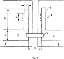
- FIG. 4 an enlarged view of the board to board interconnecting arrangement is shown in Figure 4 .
- the width of the microstrip line 2 of each substrate 1 is denoted w
- the width of the defected ground structure 4 is denoted with a
- the length of the open stub arrangement 3 is denoted with b
- the width of the open stub arrangement 3 is dented with c .
- FIG. 5 An illustration on how the board to board interconnecting arrangement might look when viewed from a first or top side 10 of the substrate 1 and a second or bottom side 20 of the substrate 1 is shown in Figure 5 .
- Figure 6 A corresponding side view is illustrated in Figure 6 , in order to illustrate the ground layer and the "etched out" nature of the defected ground structure 4.
- a bond wire is equivalent to an inductor L that jeopardizes broadband application at microwave frequency. Compensation of the bond wire inductivity L can be achieved by adding further capacitance microstrip open stubs. This resulting circuit resembles a three element low pass structure.
- the highest cut-off frequency of the proposed structure (without DGS) can be achieved when impedance of open stubs are both 250 ⁇ ,which is equivalent to 0.04 mm width microstrip line on a so called Rogers 4003C substrate with a dielectric constant of 3.38 and a thickness of 0.508 mm.
- DGS elements 4 Although illustrated as square DGS elements 4, it is possible to design and etch DGS 4 that have a non-square shape configured in dependence on the design of one or more of the particular substrates 1, microstrip lines 2 and open stub arrangements 3.
- Figure 8 illustrates a lumped element equivalent circuit of the low pass structure of the board-to-board interconnecting arrangement according to the proposed technology.
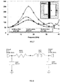
- Fig.9 a comparison of the scattering parameters or so-called S-parameters of the board-to-board interconnection of the proposed technology and a conventional approach using a single bond wire is illustrated.
- the S-parameters describe the electrical behaviour of linear electrical networks when undergoing various steady state stimuli by electrical signals. They are applicable at any frequency, but are mostly used for networks operating at radio frequency and microwave frequencies.
- Fig.10 a photograph of the top side and the bottom side of an embodiment of the proposed technology, corresponding to the schematic illustration in Fig. 5 are illustrated. In this illustration all features are presented on a single substrate, but it is easily transferred to the factual case of interconnecting two separate substrates 1.
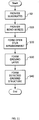
- Two coplanar substrates 1 separated by a predetermined gap g are initially provided in step S0.
- At least one bond wire 5 is provided, in step S10, across the gap to interconnect a respective conducting microstrip line 2 on a first side 10 of each substrate 1.
- at least one open stub arrangement 3 is formed, in step S20, on the first side 10 of each substrate 1, such that each open stub arrangement 3 comprises a microstrip extending at an angel from an end of each conducting microstrip line 2 on each substrate 1.
- a ground layer is formed, in step S30, on a second side 20 of each substrate 1.
- step S40 a defected ground structure 4 is formed on the second side 20 of each substrate 1 laterally overlapping each respective open stub arrangement 3.
- the steps of the embodiments can be performed in an another order. However, preferably all structures of the arrangement are provided and formed before the bond wire(s) is/are provided.
- the bond wires can be provided by soldering or other types of bonding known in the art.
- the embodiments are likewise applicable for embodiments employing one or more bond strips e.g. gold strips to interconnect the two substrates.
- the defected ground structure is formed S40 by etching away at least part of the ground layer on the second side 20 directly opposite each open stub arrangement 3.
- other methods of providing the defected ground structure can also be used.
- the proposed structure is established with open stubs by a three-stage low pass filter theory, shown in Figure 3 .
- the impedance of input/output microstrip line 2 is 50 ⁇ and open stub 3 is located at the end of each microstrip line 2.
- the only design variables are width c and length b of the open stub 3, shown in Figure 4 . Tune and optimize the two variables using Microwave simulator (AWR Microwave Office).
- Figure 8 shows the lumped element equivalent circuit of the low pass structure. Double pieces of parallel bond wires are treated as a resistor in series with an inductance, and open stubs are equivalent to capacitors.
- Step.5 Implement EM-simulation with full-wave EM-simulator (AWR AXIEM) and fabricate the circuit.
- AWR AXIEM full-wave EM-simulator
- the highest illustrated frequency is 32 GHz whereas 4 GHz is the highest frequency of a conventional single bond wire solution, S-parameters are shown in Figure 9 .
- the embodiments of the proposed technology can be beneficially used in any electronic equipment for radio frequency or microwave frequency applications where a high bandwidth is required and where it is necessary to arrange circuits on different substrates.
- Such electronic equipment can include wired or wireless devices.
- the term "wireless device” may refer to a User Equipment, UE, a mobile phone, a cellular phone, a Personal Digital Assistant, PDA, equipped with radio communication capabilities, a smart phone, a laptop or Personal Computer, PC, equipped with an internal or external mobile broadband modem, a tablet PC with radio communication capabilities, a portable electronic radio communication device, an electronic device on satellite, an electronic device on radar, an electronic device on military missile, a sensor device equipped with radio communication capabilities or the like.
- the term "UE” should be interpreted as a non-limiting term comprising any device equipped with radio circuitry for wireless communication according to any relevant communication standard.
- radio network nodes or network nodes in a telecommunication system.
- the term "radio network node” or simply “network node” may refer to base stations, network control nodes, and the like.
- the term “base station” may encompass different types of radio base stations including standardized base stations such as Node Bs, or evolved Node Bs, eNBs, and also macro/micro/pico radio base stations, home base stations, also known as femto base stations, relay nodes, repeaters, radio access points, and even radio control nodes controlling one or more Remote Radio Units, RRUs, or the like.
- embodiments may be implemented in hardware, or in software for execution by suitable processing circuitry, or a combination thereof.
Landscapes
- Engineering & Computer Science (AREA)
- Microelectronics & Electronic Packaging (AREA)
- Manufacturing & Machinery (AREA)
- Structure Of Printed Boards (AREA)
- Waveguides (AREA)
Description
- The proposed technology generally relates to wide bandwidth circuit board arrangements, and particularly to methods and arrangements for interconnecting such arrangements.
- In present day microelectronics design, one ongoing goal is to reduce the size of any integrated circuit and to fit as much functionality as possible onto a single substrate. However, due to high power signals leakage and interferers (high power local oscillation signals leak through PCB substrate to interfere transmitter/receiver part) it is sometimes necessary to separate circuits onto different substrates and sometimes it's physically impossible to fit all components onto a single circuit board, thus making it necessary to place components on different circuit boards. It is therefore important to be able to interconnect the circuits between two circuit boards or substrates whilst maintaining a high performance and avoid limiting the available bandwidth.
- One common way to interconnect circuit boards or substrates is to use bond wires or even bond strips, typically gold bond wires or strips. However, a bond wire or strip adds a low pass element to the microwave system and limits the bandwidth of the circuit. Some variants of interconnecting boards whilst enhancing the bandwidth of the board to board connection include using multiple bond wires has been shown in [1-2]. Other variants include gold bond strips [3], and a compensated microstrip line [4].
- However, as mentioned above, a bond wire adds a low pass element to the microwave system and limits the bandwidth of the circuit. Broadband interconnection using bond wires can be achieved by adopting multiple bond wires [1-2] and compensated microstrip lines [3-4].
- Using multiple golden bond wires result in cost increasing and it is impossible to use more than 5 piece bond wires due to process limitation, so the bandwidth is still limited by the limited quantity of bond wires. In a corresponding manner, the use of golden bond strip is extremely high cost due to using volume golden material. And finally, it is impossible to etch compensated microstrip line thinner than 0.1 mm due to printed circuit board (PCB) fabrication process, which limits its application. So it cannot be used on interconnection where the compensated microstrip line thinner than 0.1 mm.
- There is thus a need to provide board-to-board interconnections that enable maintaining a high bandwidth for e.g. microwave applications whilst avoiding the above-described problems.
-
US2001048155 discloses a method for making a bond-wire interconnect to pass signals between different substrates is described. According to this process, a first compensated bond wire interconnect is made to connect two substrates of a first type at an operating frequency, the first interconnect comprising a bond-wire of a fixed length and a first pair of compensation structures formed from a lowpass filter prototype. A second compensated bond wire interconnect is made to connect two substrates of a second type at the operating frequency, the second interconnect having a bond-wire of the fixed length and a second pair of compensation structures formed from the lowpass filter prototype. A bond-wire of the fixed length, one compensation structure from the first pair, and one compensation structure from the second pair, are combined to make a third compensated bond wire interconnect to connect a substrate of the first type with a substrate of the second type at the operating frequency. -
EP1783855 discloses a slot line configured with a slot formed on a front surface electrode on a dielectric substrate, and two slot lines are positioned with the front surface electrodes separated from one another with a gap therebetween. Also, a slot resonator with one end open wherein the gap side is open is provided at the front edge side of each slot line, and these slot resonators are positioned so as to be capable of coupling to one another. Further, a slot stub which is branched out from the gap side is provided on each front surface electrode. Thus, leakage of a high-frequency signal in the gap can be suppressed with the slot stub. -
US2008042775 discloses a design for a transmission line on an over split plane structure is provided, which optimizes the line length and line width of the line segment of transmission line part connected to the over split plane structure by using a concept of impedance match, such that this part of line segment behaves with a capacitive low impedance characteristic, achieving the impedance match at a designed frequency point, and thereby eliminating a discontinuous effect caused by a high impedance characteristic of the electrical property of transmission line on the over split plane structure. - It is an object to provide a solution that obviates the above-described problems.
- This and other objects are met by embodiments of the proposed technology. According to a first aspect, there is provided a wide bandwidth circuit board arrangement according to
claim 1. - According to a second aspect, there is provided a method of providing a wide bandwidth circuit board arrangement according to
claim 5. - Embodiments of the proposed technology enable interconnecting substrates whilst maintaining a high bandwidth.
- Other advantages will be appreciated when reading the detailed description.
- The embodiments, together with further objects and advantages thereof, may best be understood by referring to the following description taken together with the accompanying drawings, in which:
-
FIG. 1 is an illustration of a known board-to-board interconnection; -
FIG. 2 is an illustration of an embodiment according to the proposed technology; -
FIG. 3 is an illustration of a further embodiment according to the proposed technology; -
FIG. 4 is an enlarged section of the embodiment inFIG. 2 ; -
FIG. 5 is an illustration of two different views of the embodiment inFIG. 2 ; -
FIG. 6 is a side view of an embodiment of the proposed technology; -
FIG. 7 is a graph illustrating the effect of embodiments of the proposed technology; -
FIG. 8 is an equivalent circuit of an embodiment; -
FIG. 9 is a graph illustrating a comparison between known technology and embodiments of the proposed technology; -
FIG. 10 is a photograph of an embodiment of the proposed technology; -
FIG. 11 is a flow chart illustrating an embodiment of the proposed technology. -
- DGS
- Defected Ground Structure
- EM
- ElectroMagnetic
- LO
- Local Oscillation
- MCM
- Multi Chip Module
- MMIC
- Monolithic Microwave Integrated Circuit
- PCB
- Printed Circuit Board
- VNA
- Vector Network Analyzer
- Throughout the drawings, the same reference numbers are used for similar or corresponding elements.
- For a better understanding of the proposed technology, it may be useful to begin with a brief overview of the use of bond wires as well as the use of defected ground structures.
- Bond wires are massively used in monolithic microwave integrated circuits (MMICs) and multi-chip modules (MCMs) for signal transmission among different types of substrates. Board to board interconnection is significant important when it comes to following applications: First, to achieve higher isolation among transmitted, received and local oscillation (LO) parts of a transceiver, each part of above circuit needs to be designed on a separated circuit board to avoid signal leakage through substrate, especially LO leakage. Secondly, sometimes it's impossible to place all components on a circuit board; components must be placed on different circuit board. Conventionally, bond wire is used to interconnect board to board circuits, shown in
Fig.1 . TheFigure 1 illustrates a conventional board-to-board interconnection using a single bond wire (narrow band application below 4 GHz) - However, a bond wire adds a low pass element to the microwave system and limits the bandwidth of the system. Broadband interconnection using bond wires can be achieved by adopting multiple bond wires [1-2] and compensated microstrip lines [3-4]. But those approaches can't achieve higher frequencies exceed 20 GHz and it's impossible to etch compensated microstrip line thinner than 0.1 mm based on printed circuit board (PCB)fabrication process.
- The inventors have identified the benefits of combining bond wires and defected ground structure (DGS) to enhance the bandwidth of board to board interconnections, which at the same time overcomes the fabrication limitation of PCB's.
- The term defected ground structure (DGS) refers to the fact that it consists of a defect in the ground plane or layer of a substrate. The ground plane is typically considered to be an approximation of an infinite, perfectly-conducting current sink. Although the additional perturbations of the DGS alter the uniformity of the ground plane, they do not render it defective. The basic element of a DGS is a resonant gap or slot in the ground metal, placed directly under a transmission line and aligned for efficient coupling to the line. The equivalent circuit of a DGS is a parallel-tuned circuit in series with the transmission line to which it is coupled.
- Accordingly, with reference to
Figure 2 , an embodiment of a wide bandwidth circuit board arrangement according to the proposed technology includes twocoplanar substrates 1 separated by a predetermined gap (g). The gap does in fact include both the distance between the twosubstrates 1 as well as the respective distance of opposing ends of the microstrip of eachsubstrate 1 to the edge of thesubstrate 1. However, for simplicity reasons the gap is referred to as a board gap. The arrangement includes at least onebond wire 5 e.g.gold bond wire 5 arranged across gap and interconnecting a respectiveconducting microstrip line 2 on afirst side 10 of eachrespective substrate 1. In other words, the bond wire(s) 5 bridge the gap between the twosubstrates 1. Further, the arrangement includes at least oneopen stub arrangement 3 configured on thefirst side 10 of eachrespective substrate 1, eachopen stub arrangement 3 comprises a microstrip extending at an angle from an end of each conductingstrip 2 on eachrespective substrate 1. Thereby, theopen stub arrangement 3 is coplanar with themicrostrip 2 of each substrate and with thesubstrate 1 itself. In addition, the arrangement includes a ground layer on asecond side 20 of eachsubstrate 1. Finally, the arrangement includes a respective defectedground structure 4 arranged on thesecond side 20 of eachrespective substrate 1 and laterally overlapping each respectiveopen stub arrangement 3 arranged on thefirst side 10. This can also be described such that each defectedground structure 4 is centered directly opposite itsopen stub arrangement 3. Thereby, the defectedground structure 4 is arranged with a centre line aligned with and directly opposite of the centerline of itsopen stub arrangement 3. The defectedground structure 4 is formed by, according to a particular embodiment, etched out sections of the ground layer. - With reference to
Figure 3 , a further embodiment of the proposed technology includes multiple e.g. two, bond wires interconnecting the twosubstrates 1. Although not shown, a corresponding arrangement with three bond wires can be envisioned in a similar manner. - In order to facilitate the further understanding of the benefits and theory supporting the proposed technology, an enlarged view of the board to board interconnecting arrangement is shown in
Figure 4 . In this illustration the width of themicrostrip line 2 of eachsubstrate 1 is denoted w, the width of the defectedground structure 4 is denoted with a, the length of theopen stub arrangement 3 is denoted with b, and the width of theopen stub arrangement 3 is dented with c. - An illustration on how the board to board interconnecting arrangement might look when viewed from a first or
top side 10 of thesubstrate 1 and a second orbottom side 20 of thesubstrate 1 is shown inFigure 5 . A corresponding side view is illustrated inFigure 6 , in order to illustrate the ground layer and the "etched out" nature of the defectedground structure 4. - As mentioned, an embodiment of the proposed technology is shown in
Fig. 3 . A bond wire is equivalent to an inductor L that jeopardizes broadband application at microwave frequency. Compensation of the bond wire inductivity L can be achieved by adding further capacitance microstrip open stubs. This resulting circuit resembles a three element low pass structure. After simulation with Microwave Office, the highest cut-off frequency of the proposed structure (without DGS) can be achieved when impedance of open stubs are both 250Ω,which is equivalent to 0.04 mm width microstrip line on a so called Rogers 4003C substrate with a dielectric constant of 3.38 and a thickness of 0.508 mm. However, it's impossible to etch microstrip line thinner than 0.1 mm based on current PCB fabrication process. - To solve the problem, we proposed to etch square-shaped DGS under each open stub to achieve higher impedance without narrowing the width of the open stubs. The dependency of the impedance value Z and different length of DGS was simulated using Microwave Office, shown in
Fig.7 . Parameter "a" is the side length of a square-shaped DGS. We can see that impedance are 120 (a=1 mm), 150 (a=2 mm) and 250 Ω (a=3 mm) at 16 GHz, respectively. - Although illustrated as
square DGS elements 4, it is possible to design andetch DGS 4 that have a non-square shape configured in dependence on the design of one or more of theparticular substrates 1,microstrip lines 2 andopen stub arrangements 3. -
Figure 8 illustrates a lumped element equivalent circuit of the low pass structure of the board-to-board interconnecting arrangement according to the proposed technology. The inductance ID=L corresponds to the bond wire(s), the capacitances ID=C1, ID=C2 correspond to the respectiveopen stub arrangements 3 of eachsubstrate 1. - In
Fig.9 a comparison of the scattering parameters or so-called S-parameters of the board-to-board interconnection of the proposed technology and a conventional approach using a single bond wire is illustrated. The S-parameters describe the electrical behaviour of linear electrical networks when undergoing various steady state stimuli by electrical signals. They are applicable at any frequency, but are mostly used for networks operating at radio frequency and microwave frequencies. - In
Fig.10 a photograph of the top side and the bottom side of an embodiment of the proposed technology, corresponding to the schematic illustration inFig. 5 are illustrated. In this illustration all features are presented on a single substrate, but it is easily transferred to the factual case of interconnecting twoseparate substrates 1. - With reference to
Figure 11 an embodiment of a method of manufacturing or providing a wide bandwidth circuit board arrangement according to the proposed technology will be described. Twocoplanar substrates 1 separated by a predetermined gap g are initially provided in step S0. At least onebond wire 5 is provided, in step S10, across the gap to interconnect a respectiveconducting microstrip line 2 on afirst side 10 of eachsubstrate 1. Then, at least oneopen stub arrangement 3 is formed, in step S20, on thefirst side 10 of eachsubstrate 1, such that eachopen stub arrangement 3 comprises a microstrip extending at an angel from an end of each conductingmicrostrip line 2 on eachsubstrate 1. Further, a ground layer is formed, in step S30, on asecond side 20 of eachsubstrate 1. - Finally, in step S40, a defected
ground structure 4 is formed on thesecond side 20 of eachsubstrate 1 laterally overlapping each respectiveopen stub arrangement 3. - Although described in a particular order above the steps of the embodiments can be performed in an another order. However, preferably all structures of the arrangement are provided and formed before the bond wire(s) is/are provided. The bond wires can be provided by soldering or other types of bonding known in the art.
- In addition, although described with bond wires, the embodiments are likewise applicable for embodiments employing one or more bond strips e.g. gold strips to interconnect the two substrates.
- According to a particular embodiment the defected ground structure is formed S40 by etching away at least part of the ground layer on the
second side 20 directly opposite eachopen stub arrangement 3. However, other methods of providing the defected ground structure can also be used. - An example embodiment of a method of designing a board-to-board interconnecting arrangement with two
bond wires 5 according to the proposed technology will be described below. - The proposed structure is established with open stubs by a three-stage low pass filter theory, shown in
Figure 3 . The impedance of input/output microstrip line 2 is 50Ω andopen stub 3 is located at the end of eachmicrostrip line 2. The only design variables are width c and length b of theopen stub 3, shown inFigure 4 . Tune and optimize the two variables using Microwave simulator (AWR Microwave Office). - Create schematic diagram of the DGS structure.
Figure 8 shows the lumped element equivalent circuit of the low pass structure. Double pieces of parallel bond wires are treated as a resistor in series with an inductance, and open stubs are equivalent to capacitors. - Calculate the lumped elements equivalent circuits of the proposed low pass structure to derive the values of inductance L, resistance R and capacitance C1 and C2 as follows in Equations 1-3:


- Use a Cheyshev low pass prototype filter with a passband ripple LAr =0.1 dB, the element value are g0 =1, g1 =0.8431, g2 =0.6220, g3 =1.3554. After transferring frequency and impedance level to required value, those element value are R=55Ω, L=50 pH and C1 =C 2 =26 fF. The proposed low pass structure is implemented on a RO4003C substrate with a dielectric constant of 3.38 and a thickness of 0.508 mm.
Figure 10 shows the photograph of the proposed broadband board-to-board interconnection. - Step.5 Implement EM-simulation with full-wave EM-simulator (AWR AXIEM) and fabricate the circuit. After optimization, length b and width c of the open stub are b=2.1 mm and c=0.8 mm. To acquire a broadband transmission with input return loss less than -20dB, many dimensions need to be simulated. As shown in
Fig.9 , measured S11 is better than -20dB and S21 is better than -0.215dB blew 30GHz by e.g. Agilent N5230C network analyzer. - In the two-wire embodiment of the proposed technology the highest illustrated frequency is 32 GHz whereas 4 GHz is the highest frequency of a conventional single bond wire solution, S-parameters are shown in
Figure 9 . - The embodiments of the proposed technology can be beneficially used in any electronic equipment for radio frequency or microwave frequency applications where a high bandwidth is required and where it is necessary to arrange circuits on different substrates. Such electronic equipment can include wired or wireless devices. As used herein, the term "wireless device" may refer to a User Equipment, UE, a mobile phone, a cellular phone, a Personal Digital Assistant, PDA, equipped with radio communication capabilities, a smart phone, a laptop or Personal Computer, PC, equipped with an internal or external mobile broadband modem, a tablet PC with radio communication capabilities, a portable electronic radio communication device, an electronic device on satellite, an electronic device on radar, an electronic device on military missile, a sensor device equipped with radio communication capabilities or the like. In particular, the term "UE" should be interpreted as a non-limiting term comprising any device equipped with radio circuitry for wireless communication according to any relevant communication standard.
- Other examples are radio network nodes or network nodes in a telecommunication system. As used herein, the term "radio network node" or simply "network node" may refer to base stations, network control nodes, and the like. In particular, the term "base station" may encompass different types of radio base stations including standardized base stations such as Node Bs, or evolved Node Bs, eNBs, and also macro/micro/pico radio base stations, home base stations, also known as femto base stations, relay nodes, repeaters, radio access points, and even radio control nodes controlling one or more Remote Radio Units, RRUs, or the like.
- It will be appreciated that the methods and devices described above can be combined and re-arranged in a variety of ways.
- For example, embodiments may be implemented in hardware, or in software for execution by suitable processing circuitry, or a combination thereof.
- Some of the advantages with the embodiments of the proposed technology include:
- Great bandwidth enhancement: (32-4)/4=800% bandwidth enhancement.
- Overtime PCB, LTCC and LCP fabrication process: Width of microstrip line can't be less than 0.1 mm due to fabrication process limitation. The width of PCB need not to be narrow than 0.1 mm to achieve broadband interconnection.
- Harmonics suppression characteristics: saving filters for harmonics suppression and high performance.
- Cost saving: The proposed technology does not need multiple (more than 3) golden bond wires, which is s a great cost reduction due to use less gold material.
-
- [1] H. Y. Lee, Wideband characterization of mutual coupling between high density bonding wires, IEEE Trans Microwave Theory Tech 4 (1994), 265-267.
- [2] J. H. Lim, D. H. Kwon, J. S. Rieh, S. W. Kim and S. W. Hwang, RF characterization and modeling of various wire bond transitions, IEEE Trans Microwave Theory Tech 28 (2008), 265-267.
- [3] Z. Wang and J. Yang, Layout and process characteristics of LTCC substrate for microwave module, IEEE international Symposium on radio-frequency integration technology, 2009, 361-366.
- [4] T. Geist, Broadband microwave circuit interconnection, IEEE proceeding of German Microwave Conference 2010, 231 - 234
Claims (5)
- A wide bandwidth circuit board arrangement including two coplanar substrates (1) separated by a predetermined gap, comprising:
at least one bond wire (5) arranged across said gap and interconnecting a respective conducting microstrip line (2) on a first side (10) of each respective substrate (1); wherein the wide bandwidth circuit board arrangement is characterized in that the wide bandwidth circuit board arrangement comprises:at least one open stub arrangement (3) configured on said first side of each said respective substrate (1), each said open stub arrangement (3) comprising a microstrip extending at an angle from an end of each said conducting strip (2) on each respective substrate (1);a ground layer (6) on a second side (20) of each respective substrate (1); a defected ground structure (4) arranged on said second side (20) of each respective substrate (1) and laterally overlapping each respective open stub arrangement (3) arranged on said first side (10), wherein a basic element of said defected ground structure (4) is a resonant gap or slot in the ground layer (6), and said defected ground structure (4) and said open stub arrangement (3) are laterally overlapping such that a center of each defected ground structure (4) is arranged directly opposite a center of each said respective open stub arrangement (3). - The arrangement according to claim 1, comprising at least two bond wires (5).
- The arrangement according to claim 1 or 2, wherein each said open stub arrangement (3) forming an L-shaped end structure together with each said conducting strip (2).
- The arrangement according to any of claims 1-3, wherein said substrate is one of or on organic substrate, e.g., printed circuit board "PCB", or low temperature co-fired ceramic "LTCC" substrate or liquid crystal polymer "LCP" substrate.
- Method of providing a wide bandwidth circuit board arrangement including two provided coplanar substrates (1) separated by a predetermined gap, comprising the step of:
providing (S10) at least one bond wire (5) across said gap and interconnecting a respective conducting microstrip line (2) arranged on a first side (10) of each respective substrate (1); wherein the method is characterized by the steps of:forming (S20) at least one open stub arrangement (3) on said first side of each said respective substrate (1), each said open stub arrangement (3) comprising a microstrip extending at an angle from an end of each said conducting microstrip line (2) on each respective substrate (1);forming (S30) a ground layer on a second side (20) of each respective substrate (1); andforming (S40) a defected ground structure (4) on said second side (20) of each respective substrate (1) and laterally overlapping each respective open stub arrangement (3), wherein a basic element of said defected ground structure (4) is a resonant gap or slot in the ground layer (6), and said defected ground structure (4) and said open stub arrangement (3) are laterally overlapping such that a center of each defected ground structure (4) is arranged directly opposite a center of each said respective open stub arrangement (3).
Applications Claiming Priority (1)
| Application Number | Priority Date | Filing Date | Title |
|---|---|---|---|
| PCT/CN2013/086407 WO2015062067A1 (en) | 2013-11-01 | 2013-11-01 | Method and arrangement for board-to-board interconnection |
Publications (3)
| Publication Number | Publication Date |
|---|---|
| EP3063829A1 EP3063829A1 (en) | 2016-09-07 |
| EP3063829A4 EP3063829A4 (en) | 2017-06-14 |
| EP3063829B1 true EP3063829B1 (en) | 2019-06-26 |
Family
ID=53003177
Family Applications (1)
| Application Number | Title | Priority Date | Filing Date |
|---|---|---|---|
| EP13896519.9A Active EP3063829B1 (en) | 2013-11-01 | 2013-11-01 | Method and arrangement for board-to-board interconnection |
Country Status (3)
| Country | Link |
|---|---|
| US (1) | US9839118B2 (en) |
| EP (1) | EP3063829B1 (en) |
| WO (1) | WO2015062067A1 (en) |
Families Citing this family (2)
| Publication number | Priority date | Publication date | Assignee | Title |
|---|---|---|---|---|
| JP6173528B1 (en) * | 2016-06-02 | 2017-08-02 | 三菱電機株式会社 | Power converter |
| CN115986351B (en) * | 2022-11-18 | 2026-01-09 | 北京遥测技术研究所 | A microstrip bonding wire transition structure for automated micro-assembly production lines |
Family Cites Families (16)
| Publication number | Priority date | Publication date | Assignee | Title |
|---|---|---|---|---|
| US5583468A (en) * | 1995-04-03 | 1996-12-10 | Motorola, Inc. | High frequency transition from a microstrip transmission line to an MMIC coplanar waveguide |
| US5777528A (en) * | 1995-05-26 | 1998-07-07 | Motorola, Inc. | Mode suppressing coplanar waveguide transition and method |
| JP3723284B2 (en) | 1996-06-27 | 2005-12-07 | 三菱電機株式会社 | High frequency filter |
| US6426686B1 (en) * | 1999-06-16 | 2002-07-30 | Microsubstrates Corporation | Microwave circuit packages having a reduced number of vias in the substrate |
| US6759742B2 (en) * | 1999-10-12 | 2004-07-06 | The Whitaker Corporation | Interchangeable bond-wire interconnects |
| JP3735510B2 (en) * | 2000-04-18 | 2006-01-18 | 株式会社村田製作所 | Transmission line connection structure, high-frequency module, and communication device |
| JP2002009510A (en) | 2000-06-27 | 2002-01-11 | Mitsubishi Electric Corp | High frequency circuit and package |
| JP3649111B2 (en) * | 2000-10-24 | 2005-05-18 | 株式会社村田製作所 | High frequency circuit board, high frequency module using the same, and electronic device using the same |
| US6924714B2 (en) * | 2003-05-14 | 2005-08-02 | Anokiwave, Inc. | High power termination for radio frequency (RF) circuits |
| JP4056500B2 (en) * | 2004-06-28 | 2008-03-05 | 三菱電機株式会社 | Transmission line substrate and semiconductor package |
| JP4029173B2 (en) * | 2004-08-24 | 2008-01-09 | 株式会社村田製作所 | Transmission line connection structure and transmission / reception device |
| CN1825703A (en) | 2006-03-07 | 2006-08-30 | 上海大学 | UHF wave band miniaturized wide band wide beam slot antenna |
| US20080042775A1 (en) * | 2006-08-17 | 2008-02-21 | Inventec Corporation | Design for transmission line on over split plane structure |
| JP4629013B2 (en) * | 2006-09-28 | 2011-02-09 | 株式会社豊田中央研究所 | High frequency circuit board |
| TWI350717B (en) | 2007-09-20 | 2011-10-11 | Compal Electronics Inc | Layout of circuit board |
| US20100085130A1 (en) | 2008-10-03 | 2010-04-08 | Toyota Motor Engineering & Manufacturing North America, Inc. | Manufacturable tunable matching network for wire and ribbon bond compensation |
-
2013
- 2013-11-01 WO PCT/CN2013/086407 patent/WO2015062067A1/en not_active Ceased
- 2013-11-01 EP EP13896519.9A patent/EP3063829B1/en active Active
- 2013-11-01 US US15/031,369 patent/US9839118B2/en active Active
Non-Patent Citations (1)
| Title |
|---|
| None * |
Also Published As
| Publication number | Publication date |
|---|---|
| EP3063829A4 (en) | 2017-06-14 |
| WO2015062067A1 (en) | 2015-05-07 |
| US9839118B2 (en) | 2017-12-05 |
| US20160249447A1 (en) | 2016-08-25 |
| EP3063829A1 (en) | 2016-09-07 |
Similar Documents
| Publication | Publication Date | Title |
|---|---|---|
| Chen et al. | Synthetic quasi-TEM meandered transmission lines for compacted microwave integrated circuits | |
| Lim et al. | Design of low-pass filters using defected ground structure | |
| CN107154524B (en) | Transition structure from dielectric integrated suspension circuit to rectangular waveguide | |
| CN112928408B (en) | LTCC technology-based 5G communication frequency band-pass filter | |
| CN105990630A (en) | High-selectivity Balun band pass filter based on substrate integrated waveguide | |
| CN105514545A (en) | Compact type wide stopband high-selectivity microstrip filter | |
| Koziel et al. | Compact cell topology selection for size‐reduction‐oriented design of microstrip rat‐race couplers | |
| Ooi | Compact EBG in-phase hybrid-ring equal power divider | |
| Chen et al. | A fully integrated arbitrary power divider on printed circuit board by a novel SMD-resistor-free isolation network | |
| Sekar et al. | A novel compact dual-band half-mode substrate integrated waveguide bandpass filter | |
| US9839118B2 (en) | Method and arrangement for board-to-board interconnection | |
| Han et al. | Surface mounted parallel coupled microstrip bandpass filter with vertical transition for 5G millimeter wave applications | |
| Khan et al. | Analysis and realization of defected ground structure (DGS) on bandpass filter | |
| Decrossas et al. | Broad frequency LTCC vertical interconnect transition for multichip modules and system on package applications | |
| Beeresha et al. | CPW to microstrip transition using different CPW ground plane structures | |
| Menzel et al. | Miniaturized suspended stripline filters for integration into extended circuits | |
| CN105552492A (en) | Microstrip duplexer applied to WLAN system | |
| Khan et al. | Parametric effect of defected ground structure (DGS) on frequency of a bandpass filter | |
| Ting et al. | A low-loss via-free ridge air-filled substrate integrated waveguide on printed circuits board for mmWave application | |
| Wu et al. | A wideband noise-isolation bandstop power distribution network using quarter-wavelength line-based structure | |
| CN113314816B (en) | A composite dielectric millimeter wave filter based on multi-layer technology | |
| Mueller | SMD-type 42 GHz waveguide filter | |
| Guo et al. | A LTCC-based Ku-band 3D bandpass filter using stepped-impedance hairpin resonators | |
| US9941562B2 (en) | Microwave-frequency filtering structures | |
| Liu et al. | Miniaturized quarter-wavelength resonator for common-mode filter based on pattern ground structure |
Legal Events
| Date | Code | Title | Description |
|---|---|---|---|
| PUAI | Public reference made under article 153(3) epc to a published international application that has entered the european phase |
Free format text: ORIGINAL CODE: 0009012 |
|
| 17P | Request for examination filed |
Effective date: 20160511 |
|
| AK | Designated contracting states |
Kind code of ref document: A1 Designated state(s): AL AT BE BG CH CY CZ DE DK EE ES FI FR GB GR HR HU IE IS IT LI LT LU LV MC MK MT NL NO PL PT RO RS SE SI SK SM TR |
|
| AX | Request for extension of the european patent |
Extension state: BA ME |
|
| DAX | Request for extension of the european patent (deleted) | ||
| A4 | Supplementary search report drawn up and despatched |
Effective date: 20170517 |
|
| RIC1 | Information provided on ipc code assigned before grant |
Ipc: H01Q 1/38 20060101AFI20170511BHEP Ipc: H01P 5/02 20060101ALI20170511BHEP |
|
| STAA | Information on the status of an ep patent application or granted ep patent |
Free format text: STATUS: REQUEST FOR EXAMINATION WAS MADE |
|
| GRAP | Despatch of communication of intention to grant a patent |
Free format text: ORIGINAL CODE: EPIDOSNIGR1 |
|
| STAA | Information on the status of an ep patent application or granted ep patent |
Free format text: STATUS: GRANT OF PATENT IS INTENDED |
|
| RIC1 | Information provided on ipc code assigned before grant |
Ipc: H01Q 1/48 20060101ALI20190306BHEP Ipc: H01P 5/02 20060101ALI20190306BHEP Ipc: H05K 1/11 20060101ALI20190306BHEP Ipc: H05K 1/02 20060101ALI20190306BHEP Ipc: H01Q 1/38 20060101AFI20190306BHEP Ipc: H05K 1/14 20060101ALI20190306BHEP Ipc: H01Q 1/22 20060101ALI20190306BHEP |
|
| INTG | Intention to grant announced |
Effective date: 20190325 |
|
| GRAS | Grant fee paid |
Free format text: ORIGINAL CODE: EPIDOSNIGR3 |
|
| GRAA | (expected) grant |
Free format text: ORIGINAL CODE: 0009210 |
|
| STAA | Information on the status of an ep patent application or granted ep patent |
Free format text: STATUS: THE PATENT HAS BEEN GRANTED |
|
| AK | Designated contracting states |
Kind code of ref document: B1 Designated state(s): AL AT BE BG CH CY CZ DE DK EE ES FI FR GB GR HR HU IE IS IT LI LT LU LV MC MK MT NL NO PL PT RO RS SE SI SK SM TR |
|
| REG | Reference to a national code |
Ref country code: GB Ref legal event code: FG4D |
|
| REG | Reference to a national code |
Ref country code: CH Ref legal event code: EP |
|
| REG | Reference to a national code |
Ref country code: DE Ref legal event code: R096 Ref document number: 602013057271 Country of ref document: DE |
|
| REG | Reference to a national code |
Ref country code: AT Ref legal event code: REF Ref document number: 1149365 Country of ref document: AT Kind code of ref document: T Effective date: 20190715 |
|
| REG | Reference to a national code |
Ref country code: IE Ref legal event code: FG4D |
|
| REG | Reference to a national code |
Ref country code: NL Ref legal event code: MP Effective date: 20190626 |
|
| PG25 | Lapsed in a contracting state [announced via postgrant information from national office to epo] |
Ref country code: NO Free format text: LAPSE BECAUSE OF FAILURE TO SUBMIT A TRANSLATION OF THE DESCRIPTION OR TO PAY THE FEE WITHIN THE PRESCRIBED TIME-LIMIT Effective date: 20190926 Ref country code: LT Free format text: LAPSE BECAUSE OF FAILURE TO SUBMIT A TRANSLATION OF THE DESCRIPTION OR TO PAY THE FEE WITHIN THE PRESCRIBED TIME-LIMIT Effective date: 20190626 Ref country code: HR Free format text: LAPSE BECAUSE OF FAILURE TO SUBMIT A TRANSLATION OF THE DESCRIPTION OR TO PAY THE FEE WITHIN THE PRESCRIBED TIME-LIMIT Effective date: 20190626 Ref country code: SE Free format text: LAPSE BECAUSE OF FAILURE TO SUBMIT A TRANSLATION OF THE DESCRIPTION OR TO PAY THE FEE WITHIN THE PRESCRIBED TIME-LIMIT Effective date: 20190626 Ref country code: AL Free format text: LAPSE BECAUSE OF FAILURE TO SUBMIT A TRANSLATION OF THE DESCRIPTION OR TO PAY THE FEE WITHIN THE PRESCRIBED TIME-LIMIT Effective date: 20190626 Ref country code: FI Free format text: LAPSE BECAUSE OF FAILURE TO SUBMIT A TRANSLATION OF THE DESCRIPTION OR TO PAY THE FEE WITHIN THE PRESCRIBED TIME-LIMIT Effective date: 20190626 |
|
| REG | Reference to a national code |
Ref country code: LT Ref legal event code: MG4D |
|
| PG25 | Lapsed in a contracting state [announced via postgrant information from national office to epo] |
Ref country code: LV Free format text: LAPSE BECAUSE OF FAILURE TO SUBMIT A TRANSLATION OF THE DESCRIPTION OR TO PAY THE FEE WITHIN THE PRESCRIBED TIME-LIMIT Effective date: 20190626 Ref country code: GR Free format text: LAPSE BECAUSE OF FAILURE TO SUBMIT A TRANSLATION OF THE DESCRIPTION OR TO PAY THE FEE WITHIN THE PRESCRIBED TIME-LIMIT Effective date: 20190927 Ref country code: BG Free format text: LAPSE BECAUSE OF FAILURE TO SUBMIT A TRANSLATION OF THE DESCRIPTION OR TO PAY THE FEE WITHIN THE PRESCRIBED TIME-LIMIT Effective date: 20190926 Ref country code: RS Free format text: LAPSE BECAUSE OF FAILURE TO SUBMIT A TRANSLATION OF THE DESCRIPTION OR TO PAY THE FEE WITHIN THE PRESCRIBED TIME-LIMIT Effective date: 20190626 |
|
| REG | Reference to a national code |
Ref country code: AT Ref legal event code: MK05 Ref document number: 1149365 Country of ref document: AT Kind code of ref document: T Effective date: 20190626 |
|
| PG25 | Lapsed in a contracting state [announced via postgrant information from national office to epo] |
Ref country code: CZ Free format text: LAPSE BECAUSE OF FAILURE TO SUBMIT A TRANSLATION OF THE DESCRIPTION OR TO PAY THE FEE WITHIN THE PRESCRIBED TIME-LIMIT Effective date: 20190626 Ref country code: RO Free format text: LAPSE BECAUSE OF FAILURE TO SUBMIT A TRANSLATION OF THE DESCRIPTION OR TO PAY THE FEE WITHIN THE PRESCRIBED TIME-LIMIT Effective date: 20190626 Ref country code: PT Free format text: LAPSE BECAUSE OF FAILURE TO SUBMIT A TRANSLATION OF THE DESCRIPTION OR TO PAY THE FEE WITHIN THE PRESCRIBED TIME-LIMIT Effective date: 20191028 Ref country code: SK Free format text: LAPSE BECAUSE OF FAILURE TO SUBMIT A TRANSLATION OF THE DESCRIPTION OR TO PAY THE FEE WITHIN THE PRESCRIBED TIME-LIMIT Effective date: 20190626 Ref country code: NL Free format text: LAPSE BECAUSE OF FAILURE TO SUBMIT A TRANSLATION OF THE DESCRIPTION OR TO PAY THE FEE WITHIN THE PRESCRIBED TIME-LIMIT Effective date: 20190626 Ref country code: AT Free format text: LAPSE BECAUSE OF FAILURE TO SUBMIT A TRANSLATION OF THE DESCRIPTION OR TO PAY THE FEE WITHIN THE PRESCRIBED TIME-LIMIT Effective date: 20190626 Ref country code: EE Free format text: LAPSE BECAUSE OF FAILURE TO SUBMIT A TRANSLATION OF THE DESCRIPTION OR TO PAY THE FEE WITHIN THE PRESCRIBED TIME-LIMIT Effective date: 20190626 |
|
| PG25 | Lapsed in a contracting state [announced via postgrant information from national office to epo] |
Ref country code: IT Free format text: LAPSE BECAUSE OF FAILURE TO SUBMIT A TRANSLATION OF THE DESCRIPTION OR TO PAY THE FEE WITHIN THE PRESCRIBED TIME-LIMIT Effective date: 20190626 Ref country code: ES Free format text: LAPSE BECAUSE OF FAILURE TO SUBMIT A TRANSLATION OF THE DESCRIPTION OR TO PAY THE FEE WITHIN THE PRESCRIBED TIME-LIMIT Effective date: 20190626 Ref country code: SM Free format text: LAPSE BECAUSE OF FAILURE TO SUBMIT A TRANSLATION OF THE DESCRIPTION OR TO PAY THE FEE WITHIN THE PRESCRIBED TIME-LIMIT Effective date: 20190626 Ref country code: IS Free format text: LAPSE BECAUSE OF FAILURE TO SUBMIT A TRANSLATION OF THE DESCRIPTION OR TO PAY THE FEE WITHIN THE PRESCRIBED TIME-LIMIT Effective date: 20191026 |
|
| PG25 | Lapsed in a contracting state [announced via postgrant information from national office to epo] |
Ref country code: TR Free format text: LAPSE BECAUSE OF FAILURE TO SUBMIT A TRANSLATION OF THE DESCRIPTION OR TO PAY THE FEE WITHIN THE PRESCRIBED TIME-LIMIT Effective date: 20190626 |
|
| PG25 | Lapsed in a contracting state [announced via postgrant information from national office to epo] |
Ref country code: PL Free format text: LAPSE BECAUSE OF FAILURE TO SUBMIT A TRANSLATION OF THE DESCRIPTION OR TO PAY THE FEE WITHIN THE PRESCRIBED TIME-LIMIT Effective date: 20190626 Ref country code: DK Free format text: LAPSE BECAUSE OF FAILURE TO SUBMIT A TRANSLATION OF THE DESCRIPTION OR TO PAY THE FEE WITHIN THE PRESCRIBED TIME-LIMIT Effective date: 20190626 |
|
| PG25 | Lapsed in a contracting state [announced via postgrant information from national office to epo] |
Ref country code: IS Free format text: LAPSE BECAUSE OF FAILURE TO SUBMIT A TRANSLATION OF THE DESCRIPTION OR TO PAY THE FEE WITHIN THE PRESCRIBED TIME-LIMIT Effective date: 20200224 |
|
| REG | Reference to a national code |
Ref country code: DE Ref legal event code: R097 Ref document number: 602013057271 Country of ref document: DE |
|
| REG | Reference to a national code |
Ref country code: CH Ref legal event code: PL |
|
| PLBE | No opposition filed within time limit |
Free format text: ORIGINAL CODE: 0009261 |
|
| STAA | Information on the status of an ep patent application or granted ep patent |
Free format text: STATUS: NO OPPOSITION FILED WITHIN TIME LIMIT |
|
| PG2D | Information on lapse in contracting state deleted |
Ref country code: IS |
|
| PG25 | Lapsed in a contracting state [announced via postgrant information from national office to epo] |
Ref country code: MC Free format text: LAPSE BECAUSE OF FAILURE TO SUBMIT A TRANSLATION OF THE DESCRIPTION OR TO PAY THE FEE WITHIN THE PRESCRIBED TIME-LIMIT Effective date: 20190626 Ref country code: LU Free format text: LAPSE BECAUSE OF NON-PAYMENT OF DUE FEES Effective date: 20191101 Ref country code: CH Free format text: LAPSE BECAUSE OF NON-PAYMENT OF DUE FEES Effective date: 20191130 Ref country code: LI Free format text: LAPSE BECAUSE OF NON-PAYMENT OF DUE FEES Effective date: 20191130 |
|
| 26N | No opposition filed |
Effective date: 20200603 |
|
| REG | Reference to a national code |
Ref country code: BE Ref legal event code: MM Effective date: 20191130 |
|
| PG25 | Lapsed in a contracting state [announced via postgrant information from national office to epo] |
Ref country code: SI Free format text: LAPSE BECAUSE OF FAILURE TO SUBMIT A TRANSLATION OF THE DESCRIPTION OR TO PAY THE FEE WITHIN THE PRESCRIBED TIME-LIMIT Effective date: 20190626 |
|
| PG25 | Lapsed in a contracting state [announced via postgrant information from national office to epo] |
Ref country code: IE Free format text: LAPSE BECAUSE OF NON-PAYMENT OF DUE FEES Effective date: 20191101 |
|
| PG25 | Lapsed in a contracting state [announced via postgrant information from national office to epo] |
Ref country code: BE Free format text: LAPSE BECAUSE OF NON-PAYMENT OF DUE FEES Effective date: 20191130 |
|
| PG25 | Lapsed in a contracting state [announced via postgrant information from national office to epo] |
Ref country code: CY Free format text: LAPSE BECAUSE OF FAILURE TO SUBMIT A TRANSLATION OF THE DESCRIPTION OR TO PAY THE FEE WITHIN THE PRESCRIBED TIME-LIMIT Effective date: 20190626 |
|
| PG25 | Lapsed in a contracting state [announced via postgrant information from national office to epo] |
Ref country code: HU Free format text: LAPSE BECAUSE OF FAILURE TO SUBMIT A TRANSLATION OF THE DESCRIPTION OR TO PAY THE FEE WITHIN THE PRESCRIBED TIME-LIMIT; INVALID AB INITIO Effective date: 20131101 Ref country code: MT Free format text: LAPSE BECAUSE OF FAILURE TO SUBMIT A TRANSLATION OF THE DESCRIPTION OR TO PAY THE FEE WITHIN THE PRESCRIBED TIME-LIMIT Effective date: 20190626 |
|
| PG25 | Lapsed in a contracting state [announced via postgrant information from national office to epo] |
Ref country code: MK Free format text: LAPSE BECAUSE OF FAILURE TO SUBMIT A TRANSLATION OF THE DESCRIPTION OR TO PAY THE FEE WITHIN THE PRESCRIBED TIME-LIMIT Effective date: 20190626 |
|
| PGFP | Annual fee paid to national office [announced via postgrant information from national office to epo] |
Ref country code: DE Payment date: 20251128 Year of fee payment: 13 |
|
| PGFP | Annual fee paid to national office [announced via postgrant information from national office to epo] |
Ref country code: GB Payment date: 20251127 Year of fee payment: 13 |
|
| PGFP | Annual fee paid to national office [announced via postgrant information from national office to epo] |
Ref country code: FR Payment date: 20251125 Year of fee payment: 13 |