EP3062358A1 - Thermoelectric conversion device having thermoelectric conversion element connected thereto via wiring pattern, and method for manufacturing thermoelectric conversion device having thermoelectric conversion element connected thereto via wiring pattern - Google Patents
Thermoelectric conversion device having thermoelectric conversion element connected thereto via wiring pattern, and method for manufacturing thermoelectric conversion device having thermoelectric conversion element connected thereto via wiring pattern Download PDFInfo
- Publication number
- EP3062358A1 EP3062358A1 EP14856266.3A EP14856266A EP3062358A1 EP 3062358 A1 EP3062358 A1 EP 3062358A1 EP 14856266 A EP14856266 A EP 14856266A EP 3062358 A1 EP3062358 A1 EP 3062358A1
- Authority
- EP
- European Patent Office
- Prior art keywords
- insulating substrate
- region
- connecting portions
- thermoelectric conversion
- conversion elements
- Prior art date
- Legal status (The legal status is an assumption and is not a legal conclusion. Google has not performed a legal analysis and makes no representation as to the accuracy of the status listed.)
- Withdrawn
Links
- 238000006243 chemical reaction Methods 0.000 title claims abstract description 83
- 238000000034 method Methods 0.000 title claims description 17
- 238000004519 manufacturing process Methods 0.000 title description 13
- 239000000758 substrate Substances 0.000 claims abstract description 119
- 230000008878 coupling Effects 0.000 claims abstract description 22
- 238000010168 coupling process Methods 0.000 claims abstract description 22
- 238000005859 coupling reaction Methods 0.000 claims abstract description 22
- 229910045601 alloy Inorganic materials 0.000 claims description 12
- 239000000956 alloy Substances 0.000 claims description 12
- 239000000843 powder Substances 0.000 claims description 8
- 239000003960 organic solvent Substances 0.000 claims description 6
- 239000013078 crystal Substances 0.000 claims description 5
- 238000005245 sintering Methods 0.000 claims description 4
- 239000011248 coating agent Substances 0.000 claims description 3
- 238000000576 coating method Methods 0.000 claims description 3
- 238000010438 heat treatment Methods 0.000 claims description 2
- 239000000463 material Substances 0.000 claims description 2
- 238000003825 pressing Methods 0.000 claims description 2
- 239000011810 insulating material Substances 0.000 claims 1
- 229910052751 metal Inorganic materials 0.000 description 11
- 239000002184 metal Substances 0.000 description 11
- 238000010586 diagram Methods 0.000 description 6
- XEEYBQQBJWHFJM-UHFFFAOYSA-N Iron Chemical compound [Fe] XEEYBQQBJWHFJM-UHFFFAOYSA-N 0.000 description 4
- 239000004696 Poly ether ether ketone Substances 0.000 description 4
- 229920002530 polyetherether ketone Polymers 0.000 description 4
- RYGMFSIKBFXOCR-UHFFFAOYSA-N Copper Chemical compound [Cu] RYGMFSIKBFXOCR-UHFFFAOYSA-N 0.000 description 3
- 238000001816 cooling Methods 0.000 description 3
- 229910052802 copper Inorganic materials 0.000 description 3
- 239000010949 copper Substances 0.000 description 3
- 230000000694 effects Effects 0.000 description 3
- 229910000765 intermetallic Inorganic materials 0.000 description 3
- 239000013528 metallic particle Substances 0.000 description 3
- 239000007790 solid phase Substances 0.000 description 3
- 229910016339 Bi—Sb—Te Inorganic materials 0.000 description 2
- PXHVJJICTQNCMI-UHFFFAOYSA-N Nickel Chemical compound [Ni] PXHVJJICTQNCMI-UHFFFAOYSA-N 0.000 description 2
- 229920008285 Poly(ether ketone) PEK Polymers 0.000 description 2
- BUGBHKTXTAQXES-UHFFFAOYSA-N Selenium Chemical compound [Se] BUGBHKTXTAQXES-UHFFFAOYSA-N 0.000 description 2
- 229910052782 aluminium Inorganic materials 0.000 description 2
- 238000005229 chemical vapour deposition Methods 0.000 description 2
- 230000010354 integration Effects 0.000 description 2
- 229910052742 iron Inorganic materials 0.000 description 2
- 238000002844 melting Methods 0.000 description 2
- 230000008018 melting Effects 0.000 description 2
- 230000005855 radiation Effects 0.000 description 2
- 229920005989 resin Polymers 0.000 description 2
- 239000011347 resin Substances 0.000 description 2
- 239000011669 selenium Substances 0.000 description 2
- 229920001169 thermoplastic Polymers 0.000 description 2
- 229920005992 thermoplastic resin Polymers 0.000 description 2
- 239000004416 thermosoftening plastic Substances 0.000 description 2
- 229910000809 Alumel Inorganic materials 0.000 description 1
- 229910001152 Bi alloy Inorganic materials 0.000 description 1
- 229910002909 Bi-Te Inorganic materials 0.000 description 1
- VYZAMTAEIAYCRO-UHFFFAOYSA-N Chromium Chemical compound [Cr] VYZAMTAEIAYCRO-UHFFFAOYSA-N 0.000 description 1
- 229910001006 Constantan Inorganic materials 0.000 description 1
- 229910001245 Sb alloy Inorganic materials 0.000 description 1
- 229910001370 Se alloy Inorganic materials 0.000 description 1
- 229910000676 Si alloy Inorganic materials 0.000 description 1
- XUIMIQQOPSSXEZ-UHFFFAOYSA-N Silicon Chemical compound [Si] XUIMIQQOPSSXEZ-UHFFFAOYSA-N 0.000 description 1
- 229910001215 Te alloy Inorganic materials 0.000 description 1
- 238000010521 absorption reaction Methods 0.000 description 1
- 238000005275 alloying Methods 0.000 description 1
- XAGFODPZIPBFFR-UHFFFAOYSA-N aluminium Chemical compound [Al] XAGFODPZIPBFFR-UHFFFAOYSA-N 0.000 description 1
- WATWJIUSRGPENY-UHFFFAOYSA-N antimony atom Chemical compound [Sb] WATWJIUSRGPENY-UHFFFAOYSA-N 0.000 description 1
- JCXGWMGPZLAOME-UHFFFAOYSA-N bismuth atom Chemical compound [Bi] JCXGWMGPZLAOME-UHFFFAOYSA-N 0.000 description 1
- 229910001179 chromel Inorganic materials 0.000 description 1
- 239000011889 copper foil Substances 0.000 description 1
- 238000013461 design Methods 0.000 description 1
- 230000002708 enhancing effect Effects 0.000 description 1
- 238000003475 lamination Methods 0.000 description 1
- 150000002739 metals Chemical class 0.000 description 1
- 238000013508 migration Methods 0.000 description 1
- 230000005012 migration Effects 0.000 description 1
- 239000011490 mineral wool Substances 0.000 description 1
- 238000012986 modification Methods 0.000 description 1
- 230000004048 modification Effects 0.000 description 1
- 229910052759 nickel Inorganic materials 0.000 description 1
- 229910052757 nitrogen Inorganic materials 0.000 description 1
- 239000012188 paraffin wax Substances 0.000 description 1
- 238000000059 patterning Methods 0.000 description 1
- 229910052698 phosphorus Inorganic materials 0.000 description 1
- 238000012545 processing Methods 0.000 description 1
- 230000000717 retained effect Effects 0.000 description 1
- 229910052711 selenium Inorganic materials 0.000 description 1
- 229910052710 silicon Inorganic materials 0.000 description 1
- 239000010703 silicon Substances 0.000 description 1
- 150000003505 terpenes Chemical class 0.000 description 1
- 235000007586 terpenes Nutrition 0.000 description 1
- 231100000331 toxic Toxicity 0.000 description 1
- 230000002588 toxic effect Effects 0.000 description 1
Images




Classifications
-
- H—ELECTRICITY
- H10—SEMICONDUCTOR DEVICES; ELECTRIC SOLID-STATE DEVICES NOT OTHERWISE PROVIDED FOR
- H10N—ELECTRIC SOLID-STATE DEVICES NOT OTHERWISE PROVIDED FOR
- H10N19/00—Integrated devices, or assemblies of multiple devices, comprising at least one thermoelectric or thermomagnetic element covered by groups H10N10/00 - H10N15/00
- H10N19/101—Multiple thermocouples connected in a cascade arrangement
-
- H—ELECTRICITY
- H10—SEMICONDUCTOR DEVICES; ELECTRIC SOLID-STATE DEVICES NOT OTHERWISE PROVIDED FOR
- H10N—ELECTRIC SOLID-STATE DEVICES NOT OTHERWISE PROVIDED FOR
- H10N10/00—Thermoelectric devices comprising a junction of dissimilar materials, i.e. devices exhibiting Seebeck or Peltier effects
- H10N10/10—Thermoelectric devices comprising a junction of dissimilar materials, i.e. devices exhibiting Seebeck or Peltier effects operating with only the Peltier or Seebeck effects
- H10N10/17—Thermoelectric devices comprising a junction of dissimilar materials, i.e. devices exhibiting Seebeck or Peltier effects operating with only the Peltier or Seebeck effects characterised by the structure or configuration of the cell or thermocouple forming the device
-
- H—ELECTRICITY
- H10—SEMICONDUCTOR DEVICES; ELECTRIC SOLID-STATE DEVICES NOT OTHERWISE PROVIDED FOR
- H10N—ELECTRIC SOLID-STATE DEVICES NOT OTHERWISE PROVIDED FOR
- H10N10/00—Thermoelectric devices comprising a junction of dissimilar materials, i.e. devices exhibiting Seebeck or Peltier effects
- H10N10/01—Manufacture or treatment
-
- H—ELECTRICITY
- H10—SEMICONDUCTOR DEVICES; ELECTRIC SOLID-STATE DEVICES NOT OTHERWISE PROVIDED FOR
- H10N—ELECTRIC SOLID-STATE DEVICES NOT OTHERWISE PROVIDED FOR
- H10N10/00—Thermoelectric devices comprising a junction of dissimilar materials, i.e. devices exhibiting Seebeck or Peltier effects
- H10N10/80—Constructional details
-
- H—ELECTRICITY
- H10—SEMICONDUCTOR DEVICES; ELECTRIC SOLID-STATE DEVICES NOT OTHERWISE PROVIDED FOR
- H10N—ELECTRIC SOLID-STATE DEVICES NOT OTHERWISE PROVIDED FOR
- H10N10/00—Thermoelectric devices comprising a junction of dissimilar materials, i.e. devices exhibiting Seebeck or Peltier effects
- H10N10/80—Constructional details
- H10N10/85—Thermoelectric active materials
- H10N10/851—Thermoelectric active materials comprising inorganic compositions
- H10N10/852—Thermoelectric active materials comprising inorganic compositions comprising tellurium, selenium or sulfur
-
- H—ELECTRICITY
- H10—SEMICONDUCTOR DEVICES; ELECTRIC SOLID-STATE DEVICES NOT OTHERWISE PROVIDED FOR
- H10N—ELECTRIC SOLID-STATE DEVICES NOT OTHERWISE PROVIDED FOR
- H10N10/00—Thermoelectric devices comprising a junction of dissimilar materials, i.e. devices exhibiting Seebeck or Peltier effects
- H10N10/80—Constructional details
- H10N10/85—Thermoelectric active materials
- H10N10/851—Thermoelectric active materials comprising inorganic compositions
- H10N10/853—Thermoelectric active materials comprising inorganic compositions comprising arsenic, antimony or bismuth
-
- H—ELECTRICITY
- H10—SEMICONDUCTOR DEVICES; ELECTRIC SOLID-STATE DEVICES NOT OTHERWISE PROVIDED FOR
- H10N—ELECTRIC SOLID-STATE DEVICES NOT OTHERWISE PROVIDED FOR
- H10N10/00—Thermoelectric devices comprising a junction of dissimilar materials, i.e. devices exhibiting Seebeck or Peltier effects
- H10N10/80—Constructional details
- H10N10/85—Thermoelectric active materials
- H10N10/851—Thermoelectric active materials comprising inorganic compositions
- H10N10/854—Thermoelectric active materials comprising inorganic compositions comprising only metals
-
- H—ELECTRICITY
- H10—SEMICONDUCTOR DEVICES; ELECTRIC SOLID-STATE DEVICES NOT OTHERWISE PROVIDED FOR
- H10N—ELECTRIC SOLID-STATE DEVICES NOT OTHERWISE PROVIDED FOR
- H10N10/00—Thermoelectric devices comprising a junction of dissimilar materials, i.e. devices exhibiting Seebeck or Peltier effects
- H10N10/80—Constructional details
- H10N10/85—Thermoelectric active materials
- H10N10/851—Thermoelectric active materials comprising inorganic compositions
- H10N10/8556—Thermoelectric active materials comprising inorganic compositions comprising compounds containing germanium or silicon
Definitions
- thermoelectric conversion technique relates to a thermoelectric conversion technique, and in particular relates to a thermoelectric converter in which thermoelectric conversion elements are connected to a wiring pattern, and a method for fabricating the thermoelectric converter.
- thermoelectric converters are widely used.
- JP-A-2009-117792 proposes a thermoelectric converter in which N- and P-type thermoelectric conversion elements are alternately connected in series via electrodes.
- the N- and P-type thermoelectric conversion elements are arranged on a plurality of respective lower metal electrodes in a rectangular-plate shape.
- the N-type thermoelectric conversion element arranged on one lower metal electrode is electrically connected, via an upper metal electrode, to the P-type thermoelectric conversion element arranged on the other lower metal electrode.
- the N- and P-type thermoelectric conversion elements are alternately connected in series via the lower and upper metal electrodes.
- thermoelectric converter when it is used as a Seebeck device, the upper metal electrode side is located in a high-temperature section while the lower metal electrode side is located in a low-temperature section. Further, in the P-type thermoelectric conversion elements, holes are diffused to a low-temperature side while, in the N-type thermoelectric conversion elements, electrons are diffused to the low-temperature side. Therefore, in the P-type thermoelectric conversion elements, the low-temperature side will have a high potential while, in the N-type thermoelectric conversion elements, a high-temperature side will have a high potential. Accordingly, the alternate and serial connection of the P- and N-type thermoelectric conversion elements can achieve high electromotive voltage.
- thermoelectric converter creates a problem that the structure and the fabrication steps are likely to be complicated, due to the use of two types, i.e., N- and P-types, of thermoelectric conversion elements.
- thermoelectric converter capable of simplifying the structure and the fabrication steps, and a method for fabricating the thermoelectric converter.
- thermoelectric converter includes a back insulating substrate (10) having a first surface (10a) on which a wiring pattern (11) is formed, a front insulating substrate (20) arranged on the first surface of the back insulating substrate and integrated with the back insulating substrate, and a plurality of thermoelectric conversion elements (30) of the same conductivity type arranged between the back and front insulating substrates and connected in series via the wiring pattern.
- the thermoelectric converter has the following characteristics.
- the wiring pattern includes a plurality of first connecting portions (11a) formed in a first region of the back insulating substrate, a plurality of second connecting portions (11b) formed in a second region of the back insulating substrate, the second region being different from the first region, and a plurality of coupling portions (11c) coupling the first connecting portions to the respective second connecting portions.
- the plurality of thermoelectric conversion elements are extended in a planar direction of the back insulating substrate and each connected to a set of first and second connecting portions. In adjacent thermoelectric conversion elements, each coupling portion is characterized by coupling the first connecting portion, connected to one of the thermoelectric conversion elements, to the second connecting portion connected to the other of the thermoelectric conversion elements.
- thermoelectric converter configured in this way is used as a Seebeck device, for example, the first region is arranged in a high-temperature section while the second region is arranged in a low-temperature section.
- each coupling portion in adjacent thermoelectric conversion elements couples the first connecting portion, connected to one of the thermoelectric conversion elements, to the second connecting portion, connected to the other of the thermoelectric conversion elements. Accordingly, if the converter is configured by thermoelectric conversion elements of only one conductivity type, a large electromotive voltage can be obtained while the structure is simplified.
- a typical example of a method for fabricating a thermoelectric converter of the present disclosure is characterized in that the method includes a step of forming a wiring pattern on a first surface of a back insulating substrate, a step of coating an electrically conductive paste (31) of one conductivity type onto a plurality of predetermined portions on a second surface (20a) opposed to the first surface of the back insulating substrate, a step of configuring a laminate (40) in which the back insulating substrate and the front insulating substrate are laminated such that the first surface of the back insulating substrate is opposed to the second surface of the front insulating substrate, and the electrically conductive paste coated onto each of the plurality of predetermined portions is brought into contact with a corresponding one of the first connecting portions and a corresponding one of the second connecting portions, and a step of integrating the laminate, while forming the thermoelectric conversion elements by sintering the electrically conductive paste by heating the laminate and pressing the laminate in a laminated direction.
- thermoelectric conversion elements With this configuration, an electrically conductive paste of only one conductivity type has to be coated to configure the thermoelectric conversion elements.
- thermoelectric conversion elements of two types P and N types
- thermoelectric converter 1 of the present embodiment is an integration of a back insulating substrate 10 and a front insulating substrate 20.
- the integrated structure has an interior where a plurality of thermoelectric conversion elements 30 of one type are arranged.
- the front insulating substrate 20 is omitted from Fig. 2 .
- the back insulating substrate 10 is formed of a thermoplastic resin film having a rectangular shape in plan view.
- the thermoplastic film is made of polyether ether ketone (PEEK) or polyether ketone (PEK).
- the back insulating substrate 10 has a surface 10a on which a wiring pattern 11 is formed.
- the front insulating substrate 20 is formed of a thermoplastic resin film having a rectangular shape in plan view.
- the thermoplastic film is made of polyether ether ketone (PEEK) or polyether ketone (PEK).
- PEEK polyether ether ketone
- PEK polyether ketone
- the size and shape of the front insulating substrate 20 in plan view are the same as those of the back insulating substrate 10 in plan view.
- thermoelectric conversion elements 30 are located between the back and front insulating substrate 10 and 20, and extended in a planar direction of the back insulating substrate 10 (extended parallel to the surface 10a), while being serially connected to each other via the wiring pattern 11 formed on the back insulating substrate 10.
- the thermoelectric conversion elements 30 of the present embodiment are made of a metallic compound (sintered alloy) which is obtained by solid-phase sintering a Bi-Sb-Te alloy powder (metallic particles) so as to retain the crystal structure of the plurality of metallic atoms before being sintered.
- the thermoelectric conversion elements 30 are P-type thermoelectric conversion elements.
- thermoelectric conversion elements 30 which is characteristic of the present embodiment.
- the wiring pattern 11 includes a plurality of first and second connecting portions 11a and 11b, and includes coupling portions 11c each electrically connecting a corresponding one of the first connecting portions 11a to a corresponding one of the second connecting portions 11b.
- the first connecting portions 11a each have a rectangular shape in plan view.
- the back insulating substrate 10 has a first end (upper end portion as viewed in Fig. 2 or 3 ) region in the direction along the short side thereof, the direction being perpendicular to the longitudinal direction of the substrate 10, while being parallel to the planar direction of the substrate 10. In the first end region, the first connecting portions 11a are formed at regular intervals along the longitudinal direction of the back insulating substrate 10.
- the second connecting portions 11b each having a rectangular shape in plan view similar to the first connecting portions 11a, are formed by the same number as that of the first connecting portions 11a.
- the back insulating substrate 10 has a second end (lower end portion as viewed in Fig. 2 or 3 ) region which is in a direction along the short side of the back insulating substrate 10. In the second end region, the second connecting portions 11b are formed at regular intervals along the longitudinal direction of the back insulating substrate 10.
- the first end region along the short side corresponds to the first region of the present disclosure while the second end region along the short side corresponds to the second region of the present disclosure.
- the interval between the first connecting portions 11a is ensured to be equal to the interval between the second connecting portions 11b.
- the first connecting portions 11a are formed so as to face the respective second connecting portions 11b, in the direction along the short side of the back insulating substrate 10.
- a plurality of pairs of first and second connecting portions 11a and 11b are arranged in the longitudinal direction of the back insulating substrate 10, and in each of the pairs, the first connecting portion 11a is opposed to the second connecting portion 11b.
- the back insulating substrate 10 corresponds to the first insulating substrate while the front insulating substrate 20 corresponds to the second insulating substrate.
- Each of the plurality of thermoelectric conversion elements 30 is in a rod shape extended in a direction parallel to the short side of the back insulating substrate 10.
- Each of the thermoelectric conversion elements 30 has an end connected to the first connecting portion 11a of a corresponding one of the pairs of opposed first and second connecting portions 11a and 11b, and another end connected to the second connecting portion 11b of the pair.
- Each coupling portion 11c in adjacent thermoelectric conversion elements 30 is ensured to be formed so as to couple the first connecting portion 11a connected to one of the thermoelectric conversion elements 30 to the second connecting portion 11b connected to the other of the thermoelectric conversion elements 30.
- thermoelectric conversion element 30 a thermoelectric conversion element 30 , a first connecting portion 11a and a coupling portion 11c are repeatedly connected in this order to thereby connect the plurality of thermoelectric conversion elements 30 in series.
- the back insulating substrate 10 includes a contact portion formed being electrically connected to an external circuit.
- the contact portion is formed so as to be electrically connected to the first and second contacting portions 11a and 11b (the upper left first connecting portion 11a and the lower right connecting portion 11b as viewed in Fig. 2 or 3 ) which are not connected to the coupling portions 11c in the wiring pattern 11.
- thermoelectric converter 1 of the present embodiment is configured as described above. Referring now to Figs. 4A to 4D , a method for fabricating the thermoelectric converter 1 will be described. Figs. 4A to 4D are cross-sectional views each taken along a line I-I of Fig. 2 .
- the wiring pattern 11 (see Fig. 3 ) configured as described above is formed on the surface 10a of the back insulating substrate 10.
- a metal film such as a copper foil, is formed on the surface 10a of the back insulating substrate 10 by means, for example, of CVD (chemical vapor deposition) or the like, followed by appropriately patterning the metal film.
- an electrically conductive paste 31 is coated onto a plurality of predetermined portions of a surface 20a of the front insulating substrate 20 to serve as the thermoelectric conversion elements 30 after being sintered.
- the electrically conductive paste 31 can be coated by printing or the like by placing a mask, which is provided with openings at predetermined positions, on the surface 20a of the front insulating substrate 20.
- the electrically conductive paste 31 is obtained by adding an organic solvent, such as a terpene having a melting point at ordinary temperature, to a Bi-Sb-Te alloy powder (metallic particles).
- the electrically conductive paste 31 to be used is one from which the organic solvent is evaporated while the paste 31 is being coated.
- the electrically conductive paste 31 to be used is one which will hardly have fluidity after being coated.
- the back insulating substrate 10 is laminated with the front insulating substrate 20 to configure a laminate 40.
- the front insulating substrate 20 is laminated on the back insulating substrate 10 such that each pair of opposed first and second connecting portions 11a and 11b are brought into contact with a common one of the plurality of electrically conductive paste 31 portions.
- the front insulating substrate 20 is laminated on the back insulating substrate 10 such that one end of each of the plurality of electrically conductive paste 31 portions is in contact with the first connecting portion 11a and the other end is in contact with the second connecting portion 11b.
- the laminate 40 is placed between a pair of press plates, not shown. Then, the laminate 40 is pressed in the direction of lamination from above and below, while being heated in a vacuum, for integration of the laminate 40.
- the alloy powder is compressed and solid-phase sintered, thereby forming the thermoelectric conversion elements 30 of a metallic compound (sintered alloy) that retains the crystal structure of the plurality of metallic atoms before being sintered.
- the alloy powder is compressed together with the first and second connecting portions 11a and 11b, so that each of the thermoelectric conversion elements 30 is connected to the corresponding first and second connecting portions 11a and 11b. In this way, the thermoelectric converter 1 shown in Fig. 1 is fabricated.
- a buffer made such as of rock wool paper may be placed between the laminate 40 and each of the press plates.
- thermoelectric converter 1 when used as a Seebeck device, as shown in Fig. 5A , the first end (upper end portion as viewed in Fig. 5A ) region in the short side direction of the back insulating substrate 10 is arranged on a high-temperature side while the second end (lower end portion as viewed in Fig. 5B ) region is arranged on a low-temperature side.
- thermoelectric converter 1 when used as a Peltier device, as shown in Fig. 5B , has the first end (upper end portion as viewed in Fig. 5B ) region in the short side direction of the back insulating substrate 10 arranged so as to be in contact with a member which is desired to be cooled. Further, the second end (lower end portion as viewed in Fig. 5B ) region is used such that heat is radiated therefrom.
- thermoelectric conversion elements 30 are appropriately selected to facilitate adjustment of the spacing between the opposed first and second connecting portions 11a and 11b in each pair.
- thermoelectric conversion elements 30 are arranged along the planar direction of the back insulating substrate 10, the spacing between the high-temperature side (heat-absorption side) and the low-temperature side (heat-radiation side) can be easily adjusted. In this way, the degree of freedom in layout can be improved.
- thermoelectric converter 1 may be rolled into a cylinder for use as a Peltier unit.
- the cooling side of thermoelectric converter 1 is located so as to be wound about a heat-radiation side end of the heat pipe.
- the radiation performance (cooling performance) on the heat-radiation side is improved.
- the thermoelectric converter 1 is flexible because the back and front insulating substrates 10 and 20 are each made of a resin. Accordingly, the thermoelectric converter 1 can be easily deformed in conformity with the shape of an object to be mounted.
- thermoelectric converters 1 may be used in a state of being stacked.
- the thermoelectric converters 1 shown in Fig. 1 may be just simply stacked.
- the back insulating substrate 10 of the upper thermoelectric converter 1 may be used as the front insulating substrate 20 of the lower thermoelectric converter 1.
- metals (fins) 50 such as Al or Cu, having high heat conductivity may each be arranged, as shown in Fig. 8 , between the thermoelectric converters 1. With this configuration, heat can be further efficiently absorbed and radiated.
- the first connecting portions 11a are formed on the first end region in the short side direction of the back insulating substrate 10 while the second connecting portions 11b are formed on the second end region. Further, each of the thermoelectric conversion elements 30 has an end connected to a corresponding one of the first connecting portions 11a, and has the other end connected to a corresponding one of the second connecting portions 11b.
- thermoelectric converter 1 when the thermoelectric converter 1 is arranged as shown in Fig. 5A , for example, holes diffuse to the low-temperature side of the thermoelectric conversion elements 30.
- the coupling portion 11c is formed so as to connect the first connecting portion 11a, connected to one of the thermoelectric conversion elements 30, to the second connecting portion 11b, connected to the other of the thermoelectric conversion elements 30. Accordingly, use of only the thermoelectric conversion elements 30 of the same conductivity type can achieve a large electromotive voltage while the structure is simplified.
- thermoelectric converter 1 can be fabricated by coating only one type of electrically conductive paste 31 onto the front insulating substrate 20. Therefore, compared to the method for fabricating a thermoelectric converter including two types of thermoelectric conversion elements, fabrication steps can be simplified.
- thermoelectric conversion elements 30 P-type elements are used as the thermoelectric conversion elements 30.
- highly toxic selenium which is often used in configuring N-type thermoelectric conversion elements. Accordingly, safety can be easily managed in the fabrication steps.
- thermoelectric conversion elements 30 are arranged in the planar direction of the back insulating substrate 10.
- the spacing between the first and second connecting portions 11a and 11b can be easily changed.
- the spacing between the first and second connecting portions 11a and 11b can be easily changed according to usages and thus the degree of freedom in design can be enhanced.
- the first end region in the short side direction of the back insulating substrate 10 can be arranged on the high-temperature side while the second end region can be arranged on the low-temperature side.
- the spacing between the high- and low-temperature side regions can be easily changed. Accordingly, the spacing between the high- and low-temperature side regions can be easily increased. In this case, the temperature difference between the high- and low-temperature side regions can be easily retained, thereby obtaining a large voltage.
- the first end region in the short side direction of the back insulating substrate 10 can be used for cooling, and the second end region can be used for heat radiation.
- thermal migration occurs in the planar direction of the back insulating substrate 10.
- the spacing between the cooling-side region and the radiation-side region can be easily increased, thereby enhancing the degree of freedom in layout.
- the back and front insulating substrates 10 and 20 are each made of a resin.
- the thermoelectric converter 1 can be easily deformed in conformity with an object to be mounted.
- the following description sets forth a second embodiment of the present disclosure.
- the present embodiment is different from the first embodiment in that the wiring pattern 11 has been changed. Since the rest of the configuration is similar to the first embodiment, description is omitted.
- the first and second connecting portions 11a and 11b are formed so as to be concentrically arranged at regular intervals in a circumferential direction, centering on a predetermined reference point on the surface 10a of the back insulating substrate 10.
- the first connecting portions 11a are formed on an inner-circular region while the second connecting portions 11b are formed on an outer-circular region in a circular region centering on the predetermined reference point.
- the predetermined reference point coincides with the center of the surface 10a of the back insulating substrate 10.
- the inner-circular region corresponds to the first region of the present disclosure and the outer-circular region corresponds to the second region of the present disclosure.
- the front insulating substrate 20 is omitted from Fig. 9 .
- thermoelectric conversion elements 30 are radially arranged relative to the predetermined reference point.
- thermoelectric converter 1 configured in this way can also obtain advantageous effects similar to those of the first embodiment.
- the thermoelectric converter 1 of the present embodiment is used as a Seebeck device, for example, the inner-circular side of the thermoelectric converter 1 (back insulating substrate 10) is preferably used as a high-temperature section while the outer-circular side thereof is used as a low-temperature section.
- the thermoelectric converter 1 of the present embodiment is fabricated by appropriately changing the printing range of the wiring pattern 11 and the electrically conductive paste 31. Therefore, fabrication steps will not be particularly increased compared to the first embodiment.
- the following description sets forth a third embodiment of the present disclosure.
- the present embodiment is different from the first embodiment in that the wiring pattern 11 has been changed. Since the rest of the configuration is similar to the first embodiment, description is omitted.
- the plurality of first connecting portions 11a are formed in a first end (upper end portion as viewed in Fig. 10 ) region in the longitudinal direction of the back insulating substrate 10. Specifically, in the first end region, the first connecting portions 11a are formed in a first lateral end (left end portion as viewed in Fig. 10 ) region which is in the short side direction.
- the plurality of second connecting portions 11b are formed in a second end (lower end portion as viewed in Fig. 10 ) region in the longitudinal direction of the back insulating substrate 10. Specifically, in the second end region, the second connecting portions 11b are formed in a second lateral end (right end portion as viewed in Fig. 10 ) region which is in the short side direction.
- the first lateral end region along the short side corresponds to the first region.
- the second lateral end region along the short side corresponds to the second region.
- the front insulating substrate 20 is omitted from Fig. 10 .
- thermoelectric elements 30 are each in a polyline shape so as to connect the first connecting portions 11a to the respective second connecting portions 11b.
- the coupling portions 11c are in a polyline shape along the respective thermoelectric conversion elements 30.
- thermoelectric converter 1 configured in this way can obtain advantageous effects similar to those of the first embodiment.
- the thermoelectric converter 1 of the present embodiment is used as a Seebeck device, for example, it is preferable that the first lateral end region in the short side direction in the first end region, which is in the longitudinal direction of the thermoelectric converter 1 (back insulating substrate 10), serves as a high-temperature section, and that the second lateral end region in the short side direction in the second end region, which is in the longitudinal direction, serves as a low-temperature section.
- the thermoelectric converter 1 of the present embodiment is fabricated by appropriately changing the printing range of the wiring pattern 11 and the electrically conductive paste 31. Therefore, fabrication steps will not be increased compared to the first embodiment.
- the following description sets forth a fourth embodiment of the present disclosure.
- the present embodiment is different from the third embodiment in that the wiring pattern 11 has been changed. Since the rest of the configuration is similar to the third embodiment, description is omitted.
- the plurality of second connecting portions 11b are formed in the second end (lower end portion as viewed in Fig. 11 ) region in the longitudinal direction of the back insulating substrate 10. Specifically, in the second end region, the second connecting portions 11b are formed along the longitudinal direction in a second lateral end (right end portion as viewed in Fig. 11 ) region which is in the short side direction. For the sake of clarity, the front insulating substrate 20 is omitted from Fig. 11 .
- thermoelectric conversion elements 30 are each in an L shape so as to connect the first connecting portions 11a to the respective second connecting portions 11b.
- the coupling portions 11c are in an L shape extended along the respective thermoelectric conversion elements 30.
- thermoelectric converter 1 configured in this way can obtain advantageous effects similar to those of the third embodiment.
- the thermoelectric converter 1 of the present embodiment is fabricated by appropriately changing the printing range of the wiring pattern 11 and the electrically conductive paste 31. Therefore, fabrication steps will not be increased compared to the third embodiment.
- the thermoelectric conversion elements 30 may be N-type elements made of a metallic compound (sintered alloy) which is obtained by solid-phase sintering a Bi-Te alloy powder (metallic particles) so as to retain the crystal structure of the plurality of metallic atoms before being sintered.
- the alloy powder composing the thermoelectric conversion elements 30 may be appropriately selected from materials obtained by alloying copper, constantan, chromel, alumel and the like, with iron, nickel, chrome, copper, silicon and the like.
- the alloy powder may be appropriately selected from alloys of tellurium, bismuth, antimony, or selenium, or alloys of silicon, iron, aluminum, or the like.
- the organic solvent contained in the electrically conductive paste 31 may be, for example, a paraffin or the like having a melting point of 43°C.
- the organic solvent is preferably evaporated after the step shown in Fig. 4B , for example, to minimize wet expansion of the electrically conductive paste 31.
Landscapes
- Chemical & Material Sciences (AREA)
- Inorganic Chemistry (AREA)
- Engineering & Computer Science (AREA)
- Manufacturing & Machinery (AREA)
- Powder Metallurgy (AREA)
- Cooling Or The Like Of Semiconductors Or Solid State Devices (AREA)
- Measuring Temperature Or Quantity Of Heat (AREA)
Abstract
Description
- The present disclosure relates to a thermoelectric conversion technique, and in particular relates to a thermoelectric converter in which thermoelectric conversion elements are connected to a wiring pattern, and a method for fabricating the thermoelectric converter.
- Thermoelectric converters are widely used. As an example of such a thermoelectric converter,
JP-A-2009-117792 - In such a thermoelectric converter, when it is used as a Seebeck device, the upper metal electrode side is located in a high-temperature section while the lower metal electrode side is located in a low-temperature section. Further, in the P-type thermoelectric conversion elements, holes are diffused to a low-temperature side while, in the N-type thermoelectric conversion elements, electrons are diffused to the low-temperature side. Therefore, in the P-type thermoelectric conversion elements, the low-temperature side will have a high potential while, in the N-type thermoelectric conversion elements, a high-temperature side will have a high potential. Accordingly, the alternate and serial connection of the P- and N-type thermoelectric conversion elements can achieve high electromotive voltage.
- [Patent Literature 1]
JP-A-2009-117792 - However, such a thermoelectric converter creates a problem that the structure and the fabrication steps are likely to be complicated, due to the use of two types, i.e., N- and P-types, of thermoelectric conversion elements.
- In light of the matters set forth above, the present disclosure provides a thermoelectric converter capable of simplifying the structure and the fabrication steps, and a method for fabricating the thermoelectric converter.
- A thermoelectric converter according to a typical example of the present disclosure includes a back insulating substrate (10) having a first surface (10a) on which a wiring pattern (11) is formed, a front insulating substrate (20) arranged on the first surface of the back insulating substrate and integrated with the back insulating substrate, and a plurality of thermoelectric conversion elements (30) of the same conductivity type arranged between the back and front insulating substrates and connected in series via the wiring pattern. The thermoelectric converter has the following characteristics.
- The wiring pattern includes a plurality of first connecting portions (11a) formed in a first region of the back insulating substrate, a plurality of second connecting portions (11b) formed in a second region of the back insulating substrate, the second region being different from the first region, and a plurality of coupling portions (11c) coupling the first connecting portions to the respective second connecting portions. The plurality of thermoelectric conversion elements are extended in a planar direction of the back insulating substrate and each connected to a set of first and second connecting portions. In adjacent thermoelectric conversion elements, each coupling portion is characterized by coupling the first connecting portion, connected to one of the thermoelectric conversion elements, to the second connecting portion connected to the other of the thermoelectric conversion elements.
- When the thermoelectric converter configured in this way is used as a Seebeck device, for example, the first region is arranged in a high-temperature section while the second region is arranged in a low-temperature section. In this case, each coupling portion in adjacent thermoelectric conversion elements couples the first connecting portion, connected to one of the thermoelectric conversion elements, to the second connecting portion, connected to the other of the thermoelectric conversion elements. Accordingly, if the converter is configured by thermoelectric conversion elements of only one conductivity type, a large electromotive voltage can be obtained while the structure is simplified.
- A typical example of a method for fabricating a thermoelectric converter of the present disclosure is characterized in that the method includes a step of forming a wiring pattern on a first surface of a back insulating substrate, a step of coating an electrically conductive paste (31) of one conductivity type onto a plurality of predetermined portions on a second surface (20a) opposed to the first surface of the back insulating substrate, a step of configuring a laminate (40) in which the back insulating substrate and the front insulating substrate are laminated such that the first surface of the back insulating substrate is opposed to the second surface of the front insulating substrate, and the electrically conductive paste coated onto each of the plurality of predetermined portions is brought into contact with a corresponding one of the first connecting portions and a corresponding one of the second connecting portions, and a step of integrating the laminate, while forming the thermoelectric conversion elements by sintering the electrically conductive paste by heating the laminate and pressing the laminate in a laminated direction.
- With this configuration, an electrically conductive paste of only one conductivity type has to be coated to configure the thermoelectric conversion elements. Thus, comparing with the case of fabricating a thermoelectric converter having thermoelectric conversion elements of two types (P and N types), fabrication steps can be simplified.
- It should be noted that the bracketed reference signs of individual means in this column and in the claims indicate correspondency to specific means in the embodiments described later.
-
-
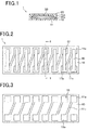
Fig. 1 is a cross-sectional view illustrating a thermoelectric converter according to a first embodiment of the present disclosure. -
Fig. 2 is a plan view illustrating the thermoelectric converter illustrated inFig. 1 . -
Fig. 3 is a plan view illustrating a back insulating substrate illustrated inFig. 1 . -
Fig. 4A is a cross-sectional view illustrating a fabrication step of the thermoelectric converter illustrated inFig. 1 . -
Fig. 4B is a cross-sectional view illustrating a fabrication step of the thermoelectric converter illustrated inFig. 1 . -
Fig. 4C is a cross-sectional view illustrating a fabrication step of the thermoelectric converter illustrated inFig. 1 . -
Fig. 4D is a cross-sectional view illustrating a fabrication step of the thermoelectric converter illustrated inFig. 1 . -
Fig. 5A is a diagram illustrating a method of using the thermoelectric converter illustrated inFig. 1 . -
Fig. 5B is a diagram illustrating a method of using the thermoelectric converter illustrated inFig. 1 . -
Fig. 6 is a diagram illustrating a method of using the thermoelectric converter illustrated inFig. 1 . -
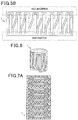
Fig. 7A is a diagram illustrating a method of using the thermoelectric converter illustrated inFig. 1 . -
Fig. 7B is a diagram illustrating a method of using the thermoelectric converter illustrated inFig. 1 . -
Fig. 8 is a diagram illustrating a method of using the thermoelectric converter illustrated inFig. 1 . -
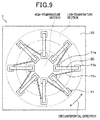
Fig. 9 is a plan view illustrating a thermoelectric converter according to a second embodiment of the present disclosure. -
Fig. 10 is a plan view illustrating a thermoelectric converter according to a third embodiment of the present disclosure. -
Fig. 11 is a plan view illustrating a thermoelectric converter according to a fourth embodiment of the present disclosure. - With reference to the accompanying drawings, hereinafter will be described some embodiments of the present disclosure. It should be noted that in the embodiments set forth below, those components which are identical or equivalent to each other are given the same reference signs.
- Referring to the drawings, a first embodiment of the present disclosure will be described. As shown in
Figs. 1 to 3 , athermoelectric converter 1 of the present embodiment is an integration of a backinsulating substrate 10 and a frontinsulating substrate 20. The integrated structure has an interior where a plurality ofthermoelectric conversion elements 30 of one type are arranged. For the sake of clarity, the frontinsulating substrate 20 is omitted fromFig. 2 . - The back insulating
substrate 10 is formed of a thermoplastic resin film having a rectangular shape in plan view. The thermoplastic film is made of polyether ether ketone (PEEK) or polyether ketone (PEK). The back insulatingsubstrate 10 has asurface 10a on which awiring pattern 11 is formed. - The front insulating
substrate 20 is formed of a thermoplastic resin film having a rectangular shape in plan view. The thermoplastic film is made of polyether ether ketone (PEEK) or polyether ketone (PEK). In the present embodiment, the size and shape of the front insulatingsubstrate 20 in plan view are the same as those of the back insulatingsubstrate 10 in plan view. - The
thermoelectric conversion elements 30 are located between the back and front insulatingsubstrate surface 10a), while being serially connected to each other via thewiring pattern 11 formed on the back insulatingsubstrate 10. Although not particularly limited, thethermoelectric conversion elements 30 of the present embodiment are made of a metallic compound (sintered alloy) which is obtained by solid-phase sintering a Bi-Sb-Te alloy powder (metallic particles) so as to retain the crystal structure of the plurality of metallic atoms before being sintered. Specifically, thethermoelectric conversion elements 30 are P-type thermoelectric conversion elements. - The following description specifically sets forth a relationship between the configuration of the
wiring pattern 11 and thethermoelectric conversion elements 30, which is characteristic of the present embodiment. - The
wiring pattern 11 includes a plurality of first and second connectingportions coupling portions 11c each electrically connecting a corresponding one of the first connectingportions 11a to a corresponding one of the second connectingportions 11b. - In the present embodiment, the first connecting
portions 11a each have a rectangular shape in plan view. The back insulatingsubstrate 10 has a first end (upper end portion as viewed inFig. 2 or 3 ) region in the direction along the short side thereof, the direction being perpendicular to the longitudinal direction of thesubstrate 10, while being parallel to the planar direction of thesubstrate 10. In the first end region, the first connectingportions 11a are formed at regular intervals along the longitudinal direction of the back insulatingsubstrate 10. - The second connecting
portions 11b, each having a rectangular shape in plan view similar to the first connectingportions 11a, are formed by the same number as that of the first connectingportions 11a. The back insulatingsubstrate 10 has a second end (lower end portion as viewed inFig. 2 or 3 ) region which is in a direction along the short side of the back insulatingsubstrate 10. In the second end region, the second connectingportions 11b are formed at regular intervals along the longitudinal direction of the back insulatingsubstrate 10. - In the present embodiment, the first end region along the short side corresponds to the first region of the present disclosure while the second end region along the short side corresponds to the second region of the present disclosure. The interval between the first connecting
portions 11a is ensured to be equal to the interval between the second connectingportions 11b. Further, the first connectingportions 11a are formed so as to face the respective second connectingportions 11b, in the direction along the short side of the back insulatingsubstrate 10. In other words, a plurality of pairs of first and second connectingportions substrate 10, and in each of the pairs, the first connectingportion 11a is opposed to the second connectingportion 11b. - It should be noted that the back insulating
substrate 10 corresponds to the first insulating substrate while the front insulatingsubstrate 20 corresponds to the second insulating substrate. - Each of the plurality of
thermoelectric conversion elements 30 is in a rod shape extended in a direction parallel to the short side of the back insulatingsubstrate 10. Each of thethermoelectric conversion elements 30 has an end connected to the first connectingportion 11a of a corresponding one of the pairs of opposed first and second connectingportions portion 11b of the pair. - Each
coupling portion 11c in adjacentthermoelectric conversion elements 30 is ensured to be formed so as to couple the first connectingportion 11a connected to one of thethermoelectric conversion elements 30 to the second connectingportion 11b connected to the other of thethermoelectric conversion elements 30. - Thus, a second connecting
portion 11b, athermoelectric conversion element 30, a first connectingportion 11a and acoupling portion 11c are repeatedly connected in this order to thereby connect the plurality ofthermoelectric conversion elements 30 in series. - In a cross section different from the one shown in
Fig. 1 , the back insulatingsubstrate 10 includes a contact portion formed being electrically connected to an external circuit. Specifically, the contact portion is formed so as to be electrically connected to the first and second contactingportions portion 11a and the lowerright connecting portion 11b as viewed inFig. 2 or 3 ) which are not connected to thecoupling portions 11c in thewiring pattern 11. - The
thermoelectric converter 1 of the present embodiment is configured as described above. Referring now toFigs. 4A to 4D , a method for fabricating thethermoelectric converter 1 will be described.Figs. 4A to 4D are cross-sectional views each taken along a line I-I ofFig. 2 . - As shown in
Fig. 4A , the wiring pattern 11 (seeFig. 3 ) configured as described above is formed on thesurface 10a of the back insulatingsubstrate 10. When forming thewiring pattern 11, a metal film, such as a copper foil, is formed on thesurface 10a of the back insulatingsubstrate 10 by means, for example, of CVD (chemical vapor deposition) or the like, followed by appropriately patterning the metal film. - In a processing step separate from the one shown in
Fig. 4A , an electricallyconductive paste 31 is coated onto a plurality of predetermined portions of asurface 20a of the front insulatingsubstrate 20 to serve as thethermoelectric conversion elements 30 after being sintered. For example, the electricallyconductive paste 31 can be coated by printing or the like by placing a mask, which is provided with openings at predetermined positions, on thesurface 20a of the front insulatingsubstrate 20. - In the present embodiment, the electrically
conductive paste 31 is obtained by adding an organic solvent, such as a terpene having a melting point at ordinary temperature, to a Bi-Sb-Te alloy powder (metallic particles). Specifically, the electricallyconductive paste 31 to be used is one from which the organic solvent is evaporated while thepaste 31 is being coated. In other words, the electricallyconductive paste 31 to be used is one which will hardly have fluidity after being coated. - Then, as shown in
Fig. 4C , the back insulatingsubstrate 10 is laminated with the front insulatingsubstrate 20 to configure a laminate 40. Specifically, the front insulatingsubstrate 20 is laminated on the back insulatingsubstrate 10 such that each pair of opposed first and second connectingportions conductive paste 31 portions. In other words, the front insulatingsubstrate 20 is laminated on the back insulatingsubstrate 10 such that one end of each of the plurality of electricallyconductive paste 31 portions is in contact with the first connectingportion 11a and the other end is in contact with the second connectingportion 11b. - Then, as shown in
Fig. 4D , the laminate 40 is placed between a pair of press plates, not shown. Then, the laminate 40 is pressed in the direction of lamination from above and below, while being heated in a vacuum, for integration of the laminate 40. In this case, the alloy powder is compressed and solid-phase sintered, thereby forming thethermoelectric conversion elements 30 of a metallic compound (sintered alloy) that retains the crystal structure of the plurality of metallic atoms before being sintered. The alloy powder is compressed together with the first and second connectingportions thermoelectric conversion elements 30 is connected to the corresponding first and second connectingportions thermoelectric converter 1 shown inFig. 1 is fabricated. - Although not particularly limited, when integrating the laminate 40, a buffer made such as of rock wool paper may be placed between the laminate 40 and each of the press plates.
- The following description sets forth a usage example of the
thermoelectric converter 1. In thethermoelectric converter 1, when used as a Seebeck device, as shown inFig. 5A , the first end (upper end portion as viewed inFig. 5A ) region in the short side direction of the back insulatingsubstrate 10 is arranged on a high-temperature side while the second end (lower end portion as viewed inFig. 5B ) region is arranged on a low-temperature side. - On the other hand, the
thermoelectric converter 1, when used as a Peltier device, as shown inFig. 5B , has the first end (upper end portion as viewed inFig. 5B ) region in the short side direction of the back insulatingsubstrate 10 arranged so as to be in contact with a member which is desired to be cooled. Further, the second end (lower end portion as viewed inFig. 5B ) region is used such that heat is radiated therefrom. - In this case, the shapes of the back and front insulating
substrates conductive paste 31 configuring thethermoelectric conversion elements 30 are appropriately selected to facilitate adjustment of the spacing between the opposed first and second connectingportions thermoelectric converter 1, since thethermoelectric conversion elements 30 are arranged along the planar direction of the back insulatingsubstrate 10, the spacing between the high-temperature side (heat-absorption side) and the low-temperature side (heat-radiation side) can be easily adjusted. In this way, the degree of freedom in layout can be improved. - As shown in
Fig. 6 , thethermoelectric converter 1 may be rolled into a cylinder for use as a Peltier unit. In this case, for example, the cooling side ofthermoelectric converter 1 is located so as to be wound about a heat-radiation side end of the heat pipe. Thus, the radiation performance (cooling performance) on the heat-radiation side is improved. In the present embodiment, thethermoelectric converter 1 is flexible because the back and front insulatingsubstrates thermoelectric converter 1 can be easily deformed in conformity with the shape of an object to be mounted. - As shown in
Fig. 7 , a plurality ofthermoelectric converters 1 may be used in a state of being stacked. In this case, as shown inFig. 7A , thethermoelectric converters 1 shown inFig. 1 may be just simply stacked. Alternatively, as shown inFig. 7B , in adjacentthermoelectric converters 1 in the stacking direction (up-and-down direction as viewed inFig. 7B ), the back insulatingsubstrate 10 of the upperthermoelectric converter 1 may be used as the front insulatingsubstrate 20 of the lowerthermoelectric converter 1. - As a modification of the stack shown in
Fig. 7A , metals (fins) 50, such as Al or Cu, having high heat conductivity may each be arranged, as shown inFig. 8 , between thethermoelectric converters 1. With this configuration, heat can be further efficiently absorbed and radiated. - As described above, according to the present embodiment, the first connecting
portions 11a are formed on the first end region in the short side direction of the back insulatingsubstrate 10 while the second connectingportions 11b are formed on the second end region. Further, each of thethermoelectric conversion elements 30 has an end connected to a corresponding one of the first connectingportions 11a, and has the other end connected to a corresponding one of the second connectingportions 11b. - Thus, when the
thermoelectric converter 1 is arranged as shown inFig. 5A , for example, holes diffuse to the low-temperature side of thethermoelectric conversion elements 30. In this regard, in adjacentthermoelectric conversion elements 30, thecoupling portion 11c is formed so as to connect the first connectingportion 11a, connected to one of thethermoelectric conversion elements 30, to the second connectingportion 11b, connected to the other of thethermoelectric conversion elements 30. Accordingly, use of only thethermoelectric conversion elements 30 of the same conductivity type can achieve a large electromotive voltage while the structure is simplified. - Being configured in this way, the
thermoelectric converter 1 can be fabricated by coating only one type of electricallyconductive paste 31 onto the front insulatingsubstrate 20. Therefore, compared to the method for fabricating a thermoelectric converter including two types of thermoelectric conversion elements, fabrication steps can be simplified. - In the present embodiment, P-type elements are used as the
thermoelectric conversion elements 30. Thus, there is no need of using highly toxic selenium which is often used in configuring N-type thermoelectric conversion elements. Accordingly, safety can be easily managed in the fabrication steps. - The
thermoelectric conversion elements 30 are arranged in the planar direction of the back insulatingsubstrate 10. Thus, for example, by appropriately changing the shape of the back insulatingsubstrate 10 in plan view, or the printing range of the electricallyconductive paste 31 configuring thethermoelectric conversion elements 30, the spacing between the first and second connectingportions portions - For example, as shown in
Fig. 5A , in a usage, the first end region in the short side direction of the back insulatingsubstrate 10 can be arranged on the high-temperature side while the second end region can be arranged on the low-temperature side. In this usage, the spacing between the high- and low-temperature side regions can be easily changed. Accordingly, the spacing between the high- and low-temperature side regions can be easily increased. In this case, the temperature difference between the high- and low-temperature side regions can be easily retained, thereby obtaining a large voltage. - As shown in
Fig. 5B , the first end region in the short side direction of the back insulatingsubstrate 10 can be used for cooling, and the second end region can be used for heat radiation. In this usage, thermal migration occurs in the planar direction of the back insulatingsubstrate 10. Thus, the spacing between the cooling-side region and the radiation-side region can be easily increased, thereby enhancing the degree of freedom in layout. - The back and front insulating
substrates thermoelectric converter 1 can be easily deformed in conformity with an object to be mounted. - The following description sets forth a second embodiment of the present disclosure. The present embodiment is different from the first embodiment in that the
wiring pattern 11 has been changed. Since the rest of the configuration is similar to the first embodiment, description is omitted. - In the present embodiment, as shown in
Fig. 9 , the first and second connectingportions surface 10a of the back insulatingsubstrate 10. In the present embodiment, the first connectingportions 11a are formed on an inner-circular region while the second connectingportions 11b are formed on an outer-circular region in a circular region centering on the predetermined reference point. - In the present embodiment, the predetermined reference point coincides with the center of the
surface 10a of the back insulatingsubstrate 10. The inner-circular region corresponds to the first region of the present disclosure and the outer-circular region corresponds to the second region of the present disclosure. For the sake of clarity, the front insulatingsubstrate 20 is omitted fromFig. 9 . - The plurality of
thermoelectric conversion elements 30 are radially arranged relative to the predetermined reference point. - The
thermoelectric converter 1 configured in this way can also obtain advantageous effects similar to those of the first embodiment. When thethermoelectric converter 1 of the present embodiment is used as a Seebeck device, for example, the inner-circular side of the thermoelectric converter 1 (back insulating substrate 10) is preferably used as a high-temperature section while the outer-circular side thereof is used as a low-temperature section. Thethermoelectric converter 1 of the present embodiment is fabricated by appropriately changing the printing range of thewiring pattern 11 and the electricallyconductive paste 31. Therefore, fabrication steps will not be particularly increased compared to the first embodiment. - The following description sets forth a third embodiment of the present disclosure. The present embodiment is different from the first embodiment in that the
wiring pattern 11 has been changed. Since the rest of the configuration is similar to the first embodiment, description is omitted. - In the present embodiment, as shown in
fig. 10 , the plurality of first connectingportions 11a are formed in a first end (upper end portion as viewed inFig. 10 ) region in the longitudinal direction of the back insulatingsubstrate 10. Specifically, in the first end region, the first connectingportions 11a are formed in a first lateral end (left end portion as viewed inFig. 10 ) region which is in the short side direction. - In contrast, the plurality of second connecting
portions 11b are formed in a second end (lower end portion as viewed inFig. 10 ) region in the longitudinal direction of the back insulatingsubstrate 10. Specifically, in the second end region, the second connectingportions 11b are formed in a second lateral end (right end portion as viewed inFig. 10 ) region which is in the short side direction. - In the present embodiment, in the first end region in the longitudinal direction of the back insulating
substrate 10, the first lateral end region along the short side corresponds to the first region. Also, in the second end region in the longitudinal direction of the back insulatingsubstrate 10, the second lateral end region along the short side corresponds to the second region. For the sake of clarity, the front insulatingsubstrate 20 is omitted fromFig. 10 . - The
thermoelectric elements 30 are each in a polyline shape so as to connect the first connectingportions 11a to the respective second connectingportions 11b. Similarly, thecoupling portions 11c are in a polyline shape along the respectivethermoelectric conversion elements 30. - The
thermoelectric converter 1 configured in this way can obtain advantageous effects similar to those of the first embodiment. When thethermoelectric converter 1 of the present embodiment is used as a Seebeck device, for example, it is preferable that the first lateral end region in the short side direction in the first end region, which is in the longitudinal direction of the thermoelectric converter 1 (back insulating substrate 10), serves as a high-temperature section, and that the second lateral end region in the short side direction in the second end region, which is in the longitudinal direction, serves as a low-temperature section. Thethermoelectric converter 1 of the present embodiment is fabricated by appropriately changing the printing range of thewiring pattern 11 and the electricallyconductive paste 31. Therefore, fabrication steps will not be increased compared to the first embodiment. - The following description sets forth a fourth embodiment of the present disclosure. The present embodiment is different from the third embodiment in that the
wiring pattern 11 has been changed. Since the rest of the configuration is similar to the third embodiment, description is omitted. - In the present embodiment, as shown in
Fig. 11 , the plurality of second connectingportions 11b are formed in the second end (lower end portion as viewed inFig. 11 ) region in the longitudinal direction of the back insulatingsubstrate 10. Specifically, in the second end region, the second connectingportions 11b are formed along the longitudinal direction in a second lateral end (right end portion as viewed inFig. 11 ) region which is in the short side direction. For the sake of clarity, the front insulatingsubstrate 20 is omitted fromFig. 11 . - The
thermoelectric conversion elements 30 are each in an L shape so as to connect the first connectingportions 11a to the respective second connectingportions 11b. Similarly, thecoupling portions 11c are in an L shape extended along the respectivethermoelectric conversion elements 30. - The
thermoelectric converter 1 configured in this way can obtain advantageous effects similar to those of the third embodiment. Thethermoelectric converter 1 of the present embodiment is fabricated by appropriately changing the printing range of thewiring pattern 11 and the electricallyconductive paste 31. Therefore, fabrication steps will not be increased compared to the third embodiment. - The present invention should not be construed as being limited to the foregoing embodiments, but can be appropriately changed within a scope of the claims.
- For example, in the foregoing embodiments, the
thermoelectric conversion elements 30 may be N-type elements made of a metallic compound (sintered alloy) which is obtained by solid-phase sintering a Bi-Te alloy powder (metallic particles) so as to retain the crystal structure of the plurality of metallic atoms before being sintered. The alloy powder composing thethermoelectric conversion elements 30 may be appropriately selected from materials obtained by alloying copper, constantan, chromel, alumel and the like, with iron, nickel, chrome, copper, silicon and the like. Alternatively, the alloy powder may be appropriately selected from alloys of tellurium, bismuth, antimony, or selenium, or alloys of silicon, iron, aluminum, or the like. - In the foregoing embodiments, the organic solvent contained in the electrically
conductive paste 31 may be, for example, a paraffin or the like having a melting point of 43°C. When using such an organic solvent, the organic solvent is preferably evaporated after the step shown inFig. 4B , for example, to minimize wet expansion of the electricallyconductive paste 31. -
- 1
- Thermoelectric converter
- 10
- Back insulating substrate
- 10a
- Surface
- 11
- Wiring pattern
- 11a
- First connecting portion
- 11b
- Second connecting portion
- 11c
- Coupling portion
- 20
- Front insulating substrate
- 20a
- Surface
- 30
- Thermoelectric conversion element
Claims (7)
- A thermoelectric converter, characterized in that the converter comprises:a first insulating substrate (10) having a first surface (10a) on which a wiring pattern (11) is formed;a second insulating substrate (20) arranged on the first surface of the first insulating substrate and integrated with the first insulating substrate; anda plurality of thermoelectric conversion elements (30) of the same conductivity type arranged between the first insulating substrate and the second insulating substrate and connected in series via the wiring pattern, wherein:the wiring pattern includes a plurality of first connecting portions (11a) formed in a first region of the first insulating substrate, a plurality of second connecting portions (11b) formed in a second region of the first insulating substrate, the second region being different from the first region, and a plurality of coupling portions (11c) coupling the first connecting portions to the second connecting portions;the plurality of thermoelectric conversion elements are extended in a planar direction of the first insulating substrate, while each being connected to a corresponding one of the first connecting portions and a corresponding one of the second connecting portions; andthe coupling portions each couple, in adjacent thermoelectric conversion elements, a first connecting portion connected to one of the thermoelectric conversion elements to a second connecting portion connected to the other of the thermoelectric conversion elements.
- The thermoelectric converter according to claim 1, characterized in that:the first insulating substrate is in a rectangular shape in plan view and includes the first region that is a first end region in a short side direction which is perpendicular to a longitudinal direction of the first insulating substrate and parallel to a planar direction of the first insulating substrate, and the second region that is a second end region opposite to the first end region;the plurality of first connecting portions are formed in the first region so as to be spaced apart from each other in the longitudinal direction; andthe plurality of second connecting portions are formed in the second region so as to be spaced apart from each other in the longitudinal direction.
- The thermoelectric converter according to claim 1, characterized in that:the first insulating substrate includes a circular region centering on a predetermined reference point, the circular region including an inner-circular region as a first region, and an outer-circular region as a second region;the plurality of first connecting portions are formed in the first region being spaced apart from each other in a circumferential direction; andthe plurality of second connecting portions are formed in the second region being spaced apart from each other in a circumferential direction.
- The thermoelectric converter according to claim 1, characterized in that:the insulating substrate is in a rectangular shape in plan view and includes, in a first end region in a longitudinal direction of the first insulating substrate, the first region that is a first lateral end region in a short side direction perpendicular to the longitudinal direction and parallel to a planar direction of the first insulating substrate, and includes, in a second end region in the longitudinal direction so as to be opposite to the first end region, the second region that is a second lateral end region in the short side direction so as to be opposite to the first lateral end region;the plurality of first connecting portions are formed in the first region so as to be spaced apart from each other along the short side direction; andthe plurality of second connecting portions are formed in the second region so as to be spaced apart from each other along the short side direction.
- The thermoelectric converter according to claim 1, characterized in that:the insulating substrate is in a rectangular shape in plan view and includes, in a first end region in a longitudinal direction of the first insulating substrate, the first region that is a first lateral end region in a short side direction perpendicular to the longitudinal direction and parallel to a planar direction of the first insulating substrate, and includes, in a second end region in the longitudinal direction so as to be opposite to the first end region, the second region that is a second lateral end region in the short side direction so as to be opposite to the first lateral end region;the plurality of first connecting portions are formed in the first region so as to be spaced apart from each other along the short side direction; andthe plurality of second connecting portions are formed in the second region so as to be spaced apart from each other along the longitudinal direction.
- A method for fabricating a thermoelectric converter, the converter comprising:a first insulating substrate (10) having a first surface (10a) on which a wiring pattern (11) is formed;a second insulating substrate (20) arranged on the first surface of the first insulating substrate and integrated with the first insulating substrate; anda plurality of thermoelectric conversion elements (30) of the same conductivity type arranged between the first insulating substrate and the second insulating substrate and connected in series via the wiring pattern, wherein:the wiring pattern includes a plurality of first connecting portions (11a) formed in a first region of the first insulating substrate, a plurality of second connecting portions (11b) formed in a second region of the first insulating substrate, the second region being different from the first region, and a plurality of coupling portions (11c) coupling the first connecting portions to the second connecting portions;the plurality of thermoelectric conversion elements are extended in a planar direction of the first insulating substrate, while each being connected to a corresponding one of the first connecting portions and a corresponding one of the second connecting portions; andthe coupling portions each couple, in adjacent thermoelectric conversion elements, a first connecting portion connected to one of the thermoelectric conversion elements to a second connecting portion connected to the other of the thermoelectric conversion elements, characterized in that the method comprises:a step of forming the wiring pattern on a first surface of the first insulating substrate;a step of coating one type of electrically conductive paste (31) onto a plurality of predetermined portions on a second surface (20a) of the second insulating substrate, the second surface being opposed to the first surface of the first insulating substrate;a step of configuring a laminate (40) in which the first insulating substrate and the second insulating substrate are laminated such that the first surface of the first insulating material is opposed to the second surface of the second insulating substrate, and the electrically conductive paste coated onto each of the plurality of predetermined portions is brought into contact with a corresponding one of the first connecting portions and a corresponding one of the second connecting portions; anda step of integrating the laminate, while forming the thermoelectric conversion elements by sintering the electrically conductive paste by heating the laminate and pressing the laminate in a laminated direction.
- The method for fabricating a thermoelectric converter according to claim 6, characterized in that:the electrically conductive paste is a pasted material obtained by adding an organic solvent to an alloy powder in which a plurality of metallic atoms retain a predetermined crystal structure; andthe step of integrating the laminate includes forming a sintered alloy, as the thermoelectric conversion elements, in which the plurality of metallic atoms are sintered in a state of retaining a crystal structure of the metallic atoms.
Applications Claiming Priority (2)
| Application Number | Priority Date | Filing Date | Title |
|---|---|---|---|
| JP2013222259A JP6024642B2 (en) | 2013-10-25 | 2013-10-25 | Thermoelectric conversion device and manufacturing method thereof |
| PCT/JP2014/077949 WO2015060301A1 (en) | 2013-10-25 | 2014-10-21 | Thermoelectric conversion device having thermoelectric conversion element connected thereto via wiring pattern, and method for manufacturing thermoelectric conversion device having thermoelectric conversion element connected thereto via wiring pattern |
Publications (2)
| Publication Number | Publication Date |
|---|---|
| EP3062358A1 true EP3062358A1 (en) | 2016-08-31 |
| EP3062358A4 EP3062358A4 (en) | 2017-05-31 |
Family
ID=52992895
Family Applications (1)
| Application Number | Title | Priority Date | Filing Date |
|---|---|---|---|
| EP14856266.3A Withdrawn EP3062358A4 (en) | 2013-10-25 | 2014-10-21 | Thermoelectric conversion device having thermoelectric conversion element connected thereto via wiring pattern, and method for manufacturing thermoelectric conversion device having thermoelectric conversion element connected thereto via wiring pattern |
Country Status (7)
| Country | Link |
|---|---|
| US (1) | US20160247995A1 (en) |
| EP (1) | EP3062358A4 (en) |
| JP (1) | JP6024642B2 (en) |
| KR (1) | KR101791473B1 (en) |
| CN (1) | CN105659399A (en) |
| TW (1) | TWI550922B (en) |
| WO (1) | WO2015060301A1 (en) |
Families Citing this family (6)
| Publication number | Priority date | Publication date | Assignee | Title |
|---|---|---|---|---|
| CN105552769A (en) * | 2014-07-18 | 2016-05-04 | 国家电网公司 | Control circuit for multifunctional electricity-verification and grounding trolley for centrally installed switchgear |
| JP2017085068A (en) * | 2015-10-30 | 2017-05-18 | 章道 中條 | A thermoelectric power generation system that generates heat by converting thermal energy into electrical energy. |
| JP6778968B2 (en) * | 2017-03-28 | 2020-11-04 | 国立研究開発法人物質・材料研究機構 | Thermoelectric cell and thermoelectric module |
| KR102335989B1 (en) * | 2017-11-29 | 2021-12-07 | 현대자동차주식회사 | Thermoelectric module sheet and thermoelectric module assembly having the same |
| JP6801752B1 (en) * | 2019-08-28 | 2020-12-16 | 東洋インキScホールディングス株式会社 | Thermoelectric conversion element |
| WO2022070929A1 (en) * | 2020-09-30 | 2022-04-07 | 日本ゼオン株式会社 | Thermoelectric conversion module and method for manufacturing thermoelectric conversion module |
Family Cites Families (10)
| Publication number | Priority date | Publication date | Assignee | Title |
|---|---|---|---|---|
| JP2005217353A (en) * | 2004-02-02 | 2005-08-11 | Yokohama Teikoki Kk | Thermoelectric semiconductor element, thermoelectric conversion module, and manufacturing method thereof |
| WO2005124881A1 (en) * | 2004-06-22 | 2005-12-29 | Aruze Corp. | Thermoelectric conversion element |
| JP2008060488A (en) * | 2006-09-04 | 2008-03-13 | Kansai Paint Co Ltd | Single-sided electrode type thermoelectric conversion module |
| JP5007748B2 (en) * | 2007-07-19 | 2012-08-22 | 株式会社村田製作所 | Thermoelectric conversion module and method for manufacturing thermoelectric conversion module |
| JP2009117792A (en) | 2007-10-19 | 2009-05-28 | Ube Ind Ltd | Thermoelectric conversion module and manufacturing method thereof |
| US20110094556A1 (en) * | 2009-10-25 | 2011-04-28 | Digital Angel Corporation | Planar thermoelectric generator |
| JP2011192923A (en) * | 2010-03-16 | 2011-09-29 | Fujitsu Ltd | Thermoelectric conversion apparatus, and method of manufacturing the same |
| JP5806316B2 (en) * | 2010-09-13 | 2015-11-10 | ピーエスティ・センサーズ・(プロプライエタリー)・リミテッドPst Sensors (Proprietary) Limited | Printed temperature sensor |
| WO2012091048A1 (en) * | 2010-12-28 | 2012-07-05 | 京セラ株式会社 | Thermoelectric conversion member |
| JP5669103B2 (en) * | 2011-03-23 | 2015-02-12 | 独立行政法人産業技術総合研究所 | Thermoelectric thin film device |
-
2013
- 2013-10-25 JP JP2013222259A patent/JP6024642B2/en not_active Expired - Fee Related
-
2014
- 2014-10-21 EP EP14856266.3A patent/EP3062358A4/en not_active Withdrawn
- 2014-10-21 WO PCT/JP2014/077949 patent/WO2015060301A1/en not_active Ceased
- 2014-10-21 KR KR1020167010143A patent/KR101791473B1/en not_active Expired - Fee Related
- 2014-10-21 CN CN201480058278.2A patent/CN105659399A/en active Pending
- 2014-10-21 US US15/031,312 patent/US20160247995A1/en not_active Abandoned
- 2014-10-24 TW TW103136784A patent/TWI550922B/en not_active IP Right Cessation
Also Published As
| Publication number | Publication date |
|---|---|
| CN105659399A (en) | 2016-06-08 |
| WO2015060301A1 (en) | 2015-04-30 |
| US20160247995A1 (en) | 2016-08-25 |
| TWI550922B (en) | 2016-09-21 |
| EP3062358A4 (en) | 2017-05-31 |
| JP2015084364A (en) | 2015-04-30 |
| JP6024642B2 (en) | 2016-11-16 |
| KR101791473B1 (en) | 2017-10-30 |
| TW201523938A (en) | 2015-06-16 |
| KR20160060097A (en) | 2016-05-27 |
Similar Documents
| Publication | Publication Date | Title |
|---|---|---|
| EP3062358A1 (en) | Thermoelectric conversion device having thermoelectric conversion element connected thereto via wiring pattern, and method for manufacturing thermoelectric conversion device having thermoelectric conversion element connected thereto via wiring pattern | |
| TWI623118B (en) | Thermoelectric conversion element | |
| CN102947960B (en) | Thermoelement | |
| US8664509B2 (en) | Thermoelectric apparatus and method of fabricating the same | |
| US20120145209A1 (en) | Thermoelectric element and thermoelectric module including the same | |
| JPWO2015045602A1 (en) | Thermoelectric module | |
| CN101587934A (en) | Thin film thermoelectric conversion module and method for manufacturing same | |
| KR20120046106A (en) | Microstructure for a seebeck effect thermoelectric generator, and method for making such a microstructure | |
| JP6553191B2 (en) | Thermoelectric conversion module | |
| KR102022429B1 (en) | Cooling thermoelectric moudule and method of manufacturing method of the same | |
| CN102832332A (en) | Flexible micro thermoelectric generator and manufacturing method thereof | |
| TW202040774A (en) | Thermoelectric conversion module | |
| JPWO2012091048A1 (en) | Thermoelectric conversion member | |
| KR101888113B1 (en) | Method for manufacturing thermoelectric conversion device | |
| KR101680422B1 (en) | Thermoelectric modules consisting of thermal-via electrodes and Fabrication method thereof | |
| CN102272956A (en) | Module having a plurality of thermoelectric elements | |
| KR20160002608A (en) | Thermoelectric modules consisting of thermal-via electrodes and Fabrication method thereof | |
| Mahfuz et al. | Performance demonstration of cavity-free planar multi-stage bileg and unileg silicon-nanowire thermoelectric generators | |
| US20180287038A1 (en) | Thermoelectric conversion device | |
| KR102019885B1 (en) | Thermoelectric module and method for manufacturing the same | |
| US20210249579A1 (en) | Flexible encapsulation of a flexible thin-film based thermoelectric device with sputter deposited layer of n-type and p-type thermoelectric legs | |
| KR102456680B1 (en) | Thermoelectric element | |
| KR20150084314A (en) | Thermoelectric modules consisting of thermal-via electrodes and Fabrication method thereof | |
| JP2019140294A (en) | Thermoelectric conversion device and manufacturing method thereof | |
| JP2018166202A (en) | Thermoelectric conversion device |
Legal Events
| Date | Code | Title | Description |
|---|---|---|---|
| PUAI | Public reference made under article 153(3) epc to a published international application that has entered the european phase |
Free format text: ORIGINAL CODE: 0009012 |
|
| 17P | Request for examination filed |
Effective date: 20160504 |
|
| AK | Designated contracting states |
Kind code of ref document: A1 Designated state(s): AL AT BE BG CH CY CZ DE DK EE ES FI FR GB GR HR HU IE IS IT LI LT LU LV MC MK MT NL NO PL PT RO RS SE SI SK SM TR |
|
| AX | Request for extension of the european patent |
Extension state: BA ME |
|
| DAX | Request for extension of the european patent (deleted) | ||
| A4 | Supplementary search report drawn up and despatched |
Effective date: 20170502 |
|
| RIC1 | Information provided on ipc code assigned before grant |
Ipc: H01L 35/34 20060101ALI20170424BHEP Ipc: H02N 11/00 20060101ALI20170424BHEP Ipc: H01L 35/32 20060101AFI20170424BHEP |
|
| STAA | Information on the status of an ep patent application or granted ep patent |
Free format text: STATUS: THE APPLICATION HAS BEEN WITHDRAWN |
|
| 18W | Application withdrawn |
Effective date: 20180720 |