EP3062335B1 - Method of intercalating an insulating layer between a metal layer and a graphene layer and method of fabricating semiconductor device using the intercalation method - Google Patents
Method of intercalating an insulating layer between a metal layer and a graphene layer and method of fabricating semiconductor device using the intercalation method Download PDFInfo
- Publication number
- EP3062335B1 EP3062335B1 EP16157047.8A EP16157047A EP3062335B1 EP 3062335 B1 EP3062335 B1 EP 3062335B1 EP 16157047 A EP16157047 A EP 16157047A EP 3062335 B1 EP3062335 B1 EP 3062335B1
- Authority
- EP
- European Patent Office
- Prior art keywords
- layer
- graphene layer
- intercalating
- graphene
- insulating layer
- Prior art date
- Legal status (The legal status is an assumption and is not a legal conclusion. Google has not performed a legal analysis and makes no representation as to the accuracy of the status listed.)
- Active
Links
Images





Classifications
-
- H—ELECTRICITY
- H10—SEMICONDUCTOR DEVICES; ELECTRIC SOLID-STATE DEVICES NOT OTHERWISE PROVIDED FOR
- H10D—INORGANIC ELECTRIC SEMICONDUCTOR DEVICES
- H10D30/00—Field-effect transistors [FET]
- H10D30/60—Insulated-gate field-effect transistors [IGFET]
- H10D30/67—Thin-film transistors [TFT]
- H10D30/6757—Thin-film transistors [TFT] characterised by the structure of the channel, e.g. transverse or longitudinal shape or doping profile
-
- H—ELECTRICITY
- H10—SEMICONDUCTOR DEVICES; ELECTRIC SOLID-STATE DEVICES NOT OTHERWISE PROVIDED FOR
- H10D—INORGANIC ELECTRIC SEMICONDUCTOR DEVICES
- H10D30/00—Field-effect transistors [FET]
- H10D30/01—Manufacture or treatment
-
- H—ELECTRICITY
- H10—SEMICONDUCTOR DEVICES; ELECTRIC SOLID-STATE DEVICES NOT OTHERWISE PROVIDED FOR
- H10D—INORGANIC ELECTRIC SEMICONDUCTOR DEVICES
- H10D62/00—Semiconductor bodies, or regions thereof, of devices having potential barriers
- H10D62/80—Semiconductor bodies, or regions thereof, of devices having potential barriers characterised by the materials
- H10D62/83—Semiconductor bodies, or regions thereof, of devices having potential barriers characterised by the materials being Group IV materials, e.g. B-doped Si or undoped Ge
- H10D62/8303—Diamond
-
- H—ELECTRICITY
- H10—SEMICONDUCTOR DEVICES; ELECTRIC SOLID-STATE DEVICES NOT OTHERWISE PROVIDED FOR
- H10D—INORGANIC ELECTRIC SEMICONDUCTOR DEVICES
- H10D62/00—Semiconductor bodies, or regions thereof, of devices having potential barriers
- H10D62/80—Semiconductor bodies, or regions thereof, of devices having potential barriers characterised by the materials
- H10D62/881—Semiconductor bodies, or regions thereof, of devices having potential barriers characterised by the materials being a two-dimensional material
- H10D62/882—Graphene
-
- H—ELECTRICITY
- H10—SEMICONDUCTOR DEVICES; ELECTRIC SOLID-STATE DEVICES NOT OTHERWISE PROVIDED FOR
- H10D—INORGANIC ELECTRIC SEMICONDUCTOR DEVICES
- H10D64/00—Electrodes of devices having potential barriers
- H10D64/01—Manufacture or treatment
- H10D64/013—Manufacture or treatment of electrodes having a conductor capacitively coupled to a semiconductor by an insulator
- H10D64/01364—Manufacture or treatment of electrodes having a conductor capacitively coupled to a semiconductor by an insulator the semiconductor being diamond, semiconducting diamond-like carbon or graphene
-
- H—ELECTRICITY
- H10—SEMICONDUCTOR DEVICES; ELECTRIC SOLID-STATE DEVICES NOT OTHERWISE PROVIDED FOR
- H10P—GENERIC PROCESSES OR APPARATUS FOR THE MANUFACTURE OR TREATMENT OF DEVICES COVERED BY CLASS H10
- H10P14/00—Formation of materials, e.g. in the shape of layers or pillars
- H10P14/20—Formation of materials, e.g. in the shape of layers or pillars of semiconductor materials
- H10P14/29—Formation of materials, e.g. in the shape of layers or pillars of semiconductor materials characterised by the substrates
- H10P14/2901—Materials
- H10P14/2923—Materials being conductive materials, e.g. metallic silicides
-
- H—ELECTRICITY
- H10—SEMICONDUCTOR DEVICES; ELECTRIC SOLID-STATE DEVICES NOT OTHERWISE PROVIDED FOR
- H10P—GENERIC PROCESSES OR APPARATUS FOR THE MANUFACTURE OR TREATMENT OF DEVICES COVERED BY CLASS H10
- H10P14/00—Formation of materials, e.g. in the shape of layers or pillars
- H10P14/20—Formation of materials, e.g. in the shape of layers or pillars of semiconductor materials
- H10P14/32—Formation of materials, e.g. in the shape of layers or pillars of semiconductor materials characterised by intermediate layers between substrates and deposited layers
- H10P14/3202—Materials thereof
- H10P14/3238—Materials thereof being insulating materials
-
- H—ELECTRICITY
- H10—SEMICONDUCTOR DEVICES; ELECTRIC SOLID-STATE DEVICES NOT OTHERWISE PROVIDED FOR
- H10P—GENERIC PROCESSES OR APPARATUS FOR THE MANUFACTURE OR TREATMENT OF DEVICES COVERED BY CLASS H10
- H10P14/00—Formation of materials, e.g. in the shape of layers or pillars
- H10P14/20—Formation of materials, e.g. in the shape of layers or pillars of semiconductor materials
- H10P14/32—Formation of materials, e.g. in the shape of layers or pillars of semiconductor materials characterised by intermediate layers between substrates and deposited layers
- H10P14/3242—Structure
- H10P14/3244—Layer structure
- H10P14/3246—Monolayers
-
- H—ELECTRICITY
- H10—SEMICONDUCTOR DEVICES; ELECTRIC SOLID-STATE DEVICES NOT OTHERWISE PROVIDED FOR
- H10P—GENERIC PROCESSES OR APPARATUS FOR THE MANUFACTURE OR TREATMENT OF DEVICES COVERED BY CLASS H10
- H10P14/00—Formation of materials, e.g. in the shape of layers or pillars
- H10P14/20—Formation of materials, e.g. in the shape of layers or pillars of semiconductor materials
- H10P14/34—Deposited materials, e.g. layers
- H10P14/3402—Deposited materials, e.g. layers characterised by the chemical composition
- H10P14/3404—Deposited materials, e.g. layers characterised by the chemical composition being Group IVA materials
- H10P14/3406—Carbon, e.g. diamond-like carbon
-
- H—ELECTRICITY
- H10—SEMICONDUCTOR DEVICES; ELECTRIC SOLID-STATE DEVICES NOT OTHERWISE PROVIDED FOR
- H10P—GENERIC PROCESSES OR APPARATUS FOR THE MANUFACTURE OR TREATMENT OF DEVICES COVERED BY CLASS H10
- H10P14/00—Formation of materials, e.g. in the shape of layers or pillars
- H10P14/20—Formation of materials, e.g. in the shape of layers or pillars of semiconductor materials
- H10P14/38—Formation of materials, e.g. in the shape of layers or pillars of semiconductor materials characterised by treatments done after the formation of the materials
-
- H—ELECTRICITY
- H10—SEMICONDUCTOR DEVICES; ELECTRIC SOLID-STATE DEVICES NOT OTHERWISE PROVIDED FOR
- H10P—GENERIC PROCESSES OR APPARATUS FOR THE MANUFACTURE OR TREATMENT OF DEVICES COVERED BY CLASS H10
- H10P14/00—Formation of materials, e.g. in the shape of layers or pillars
- H10P14/60—Formation of materials, e.g. in the shape of layers or pillars of insulating materials
- H10P14/63—Formation of materials, e.g. in the shape of layers or pillars of insulating materials characterised by the formation processes
- H10P14/6326—Deposition processes
-
- H—ELECTRICITY
- H10—SEMICONDUCTOR DEVICES; ELECTRIC SOLID-STATE DEVICES NOT OTHERWISE PROVIDED FOR
- H10P—GENERIC PROCESSES OR APPARATUS FOR THE MANUFACTURE OR TREATMENT OF DEVICES COVERED BY CLASS H10
- H10P14/00—Formation of materials, e.g. in the shape of layers or pillars
- H10P14/60—Formation of materials, e.g. in the shape of layers or pillars of insulating materials
- H10P14/69—Inorganic materials
- H10P14/692—Inorganic materials composed of oxides, glassy oxides or oxide-based glasses
- H10P14/6921—Inorganic materials composed of oxides, glassy oxides or oxide-based glasses containing silicon
- H10P14/69215—Inorganic materials composed of oxides, glassy oxides or oxide-based glasses containing silicon the material being a silicon oxide, e.g. SiO2
-
- H—ELECTRICITY
- H10—SEMICONDUCTOR DEVICES; ELECTRIC SOLID-STATE DEVICES NOT OTHERWISE PROVIDED FOR
- H10P—GENERIC PROCESSES OR APPARATUS FOR THE MANUFACTURE OR TREATMENT OF DEVICES COVERED BY CLASS H10
- H10P14/00—Formation of materials, e.g. in the shape of layers or pillars
- H10P14/60—Formation of materials, e.g. in the shape of layers or pillars of insulating materials
- H10P14/69—Inorganic materials
- H10P14/694—Inorganic materials composed of nitrides
- H10P14/6943—Inorganic materials composed of nitrides containing silicon
- H10P14/69433—Inorganic materials composed of nitrides containing silicon the material being a silicon nitride not containing oxygen, e.g. SixNy or SixByNz
Definitions
- Example embodiments relate to methods of intercalating an insulating layer between a metal and a graphene layer, and more particularly, to methods of intercalating an insulating layer between a metal and a graphene layer that is directly grown on the metal.
- Graphene is a material having a single-atom-thick two-dimensional (2D) planar sheet made of carbon atoms. Since graphene has very stable and excellent electrical/mechanical/chemical properties and has excellent conductivity, graphene has been spotlighted as a next-generation material. In particular, a study of a method of manufacturing an electronic device by using graphene, instead of a silicon semiconductor, has been conducted. For example, a transistor that uses graphene as a channel layer by combining graphene with another 2D material or combining graphene with a typical semiconductor material has been developed.
- graphene may be directly grown on a surface of a metal by using chemical vapor deposition (CVD). Accordingly, in order to use graphene in a semiconductor device or a display apparatus, transferring graphene that is grown on a metal substrate onto a surface of another material, e.g., a nonconductor may be necessary.
- Examples of a general method of transferring graphene include a method of moving graphene that remains after a metal substrate is dissolved in a liquid solvent to a surface of another material and a method of detaching graphene from a metal substrate by using a stamp having an adhesive force and attaching the graphene adhered to the stamp to a surface of another material.
- a device including an intercalated silicon or silica layer between a metal layer and a graphene layer is known from US2011/086756 .
- Example embodiments provide methods of intercalating an insulating layer between a metal and a graphene layer that is directly grown on the metal.
- Example embodiments provide methods of fabricating a semiconductor device by using the intercalation methods.
- the first material may include at least one of silicon (Si), aluminum (Al), hafnium (Hf), zirconium (Zr), and lanthanum (La).
- the second material includes at least one of oxygen (O) and nitrogen (N).
- the insulating layer is an oxide insulator or a nitride insulator.
- the insulating layer may include oxide insulator crystals or nitride insulator crystals.
- the first pressure is lower than the second pressure and the first temperature is higher than the second temperature.
- the first pressure may be equal to or lower than 10 -9 torr and the first temperature may range from about 500°C to about 550°C.
- the second pressure may range from 2 ⁇ 10 -7 torr to 8 ⁇ 10 -7 torr and the second temperature may range from about 340°C to about 400°C.
- the method may further include sequentially and repeatedly performing the intercalating of the first material and the intercalating of the second material between the graphene layer and the metal layer.
- the intercalating of the first material between the graphene layer and the metal layer may be continuously and repeatedly performed at least twice.
- the method may further include: disposing a third material, which is different from the first material and the second material, on the surface of the graphene layer; and intercalating the third material between the graphene layer and the metal layer by heating the third material at the first pressure and the first temperature, wherein after the intercalating of the second material, the third material and the second material are chemically bonded to each other such that an additional insulating layer is formed between the metal layer and the graphene layer.
- the third material may include at least one of Si, Al, Hf, Zr, and La.
- the method may further include: disposing a third material, which is different from the first material and the second material, on the surface of the graphene layer; and intercalating the third material between the graphene layer and the metal layer by heating the third material at the first pressure and the first temperature, wherein the third material and the second material are chemically bonded to each other such that an additional insulating layer is formed between the metal layer and the graphene layer.
- the method may further include patterning the graphene layer that is grown on the metal layer.
- the metal layer may include at least one metal selected from the group consisting of copper (Cu), nickel (Ni), platinum (Pt), cobalt (Co), ruthenium (Ru), aluminum (Al), iron (Fe), gold (Au), magnesium (Mg), chromium (Cr), manganese (Mn), rhodium (Rh), tantalum (Ta), titanium (Ti), iridium (Ir), uranium (U), vanadium (V), and tungsten (W).
- a method of fabricating a transistor includes growing a graphene layer on a metal layer; patterning the graphene layer; disposing a first material on a surface of the graphene layer; intercalating the first material between the graphene layer and the metal layer by heating the first material at a first pressure and a first temperature; disposing a second material over the surface of the graphene layer; intercalating the second material between the graphene layer and the metal layer by heating the second material at a second pressure and a second temperature; and forming a first electrode and a second electrode that contact both sides of the graphene layer, wherein the first material and the second material are chemically bonded to each other such that an insulating layer is formed between the metal layer and the graphene layer.
- a stacked structure includes a metal layer; an insulating layer that is disposed on the metal layer and includes a first material and a second material that are different from each other and are chemically bonded to each other; and a graphene layer that is disposed on the insulating layer, wherein the second material includes at least one of oxygen (O) and nitrogen (N), and the insulating layer includes oxide insulator crystals or nitride insulator crystals.
- the stacked structure further includes a first material-metal compound layer that is disposed between the metal layer and the insulating layer.
- first, second, third, fourth etc. may be used herein to describe various elements, components, regions, layers and/or sections, these elements, components, regions, layers and/or sections should not be limited by these terms. These terms are only used to distinguish one element, component, region, layer or section from another region, layer or section. Thus, a first element, component, region, layer or section discussed below could be termed a second element, component, region, layer or section without departing from the teachings of the present inventive concepts.
- spatially relative terms such as “beneath,” “below,” “lower,” “above,” “upper” and the like, may be used herein for ease of description to describe one element or feature's relationship to another element(s) or feature(s) as illustrated in the figures. It will be understood that the spatially relative terms are intended to encompass different orientations of the device in use or operation in addition to the orientation depicted in the figures. For example, if the device in the figures is turned over, elements described as “below” or “beneath” other elements or features would then be oriented “above” the other elements or features. Thus, the example term “below” can encompass both an orientation of above and below. The device may be otherwise oriented (rotated 90 degrees or at other orientations) and the spatially relative descriptors used herein interpreted accordingly.
- Example embodiments are described herein with reference to cross-sectional illustrations that are schematic illustrations of idealized example embodiments (and intermediate structures). As such, variations from the shapes of the illustrations as a result, for example, of manufacturing techniques and/or tolerances, are to be expected. Thus, example embodiments should not be construed as limited to the particular shapes of regions illustrated herein but are to include deviations in shapes that result, for example, from manufacturing. For example, an implanted region illustrated as a rectangle will, typically, have rounded or curved features and/or a gradient of implant concentration at its edges rather than a binary change from implanted to non-implanted region.
- a buried region formed by implantation may result in some implantation in the region between the buried region and the surface through which the implantation takes place.
- the regions illustrated in the figures are schematic in nature and their shapes are not intended to illustrate the actual shape of a region of a device and are not intended to limit the scope of the present inventive concepts.
- a graphene layer may be grown on a surface of a metal substrate by using chemical vapor deposition (CVD). Carbon atoms in the grown graphene layer are strongly sp 2 bonded to one another, whereas the graphene layer and the metal substrate are relatively weakly bonded to each other by only a van der Waals force. Accordingly, it is possible to insert a material between the graphene layer and the metal substrate under an appropriate condition. A method of additionally inserting another material between the graphene layer and the metal substrate is referred to as an intercalation method.
- an intercalation method is largely used in order to reduce the effect of the metal substrate on the graphene layer and to enable the graphene layer to behave like a freestanding one.
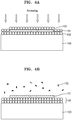
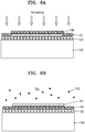
- FIGS. 1A through 1F are cross-sectional views for explaining a process of intercalating an insulating layer between a metal substrate 100 and a graphene layer 101 by using an intercalation method, according to example embodiments.
- the graphene layer 101 is grown on the metal substrate 100.
- the graphene layer 101 may be grown by using CVD.
- the metal substrate 100 may include at least one metal from among, for example, copper (Cu), nickel (Ni), platinum (Pt), cobalt (Co), ruthenium (Ru), aluminum (Al), iron (Fe), gold (Au), magnesium (Mg), chromium (Cr), manganese (Mn), rhodium (Rh), tantalum (Ta), titanium (Ti), iridium (Ir), uranium (U), vanadium (V), and tungsten (W), or an alloy thereof.
- the metal substrate 100 may have, for example, a (111) or (0001) crystalline orientation.
- the graphene layer 101 that is formed on the metal substrate 100 may be patterned to have a desired shape.
- the graphene layer 101 may be etched to have a shape suitable for a device to be fabricated.
- the patterning of the graphene layer 101 is not essential and may be omitted as desired.
- an order in which the graphene layer 101 is patterned may be changed. For example, a process of FIG. 1F is completed, and then the graphene layer 101 may be patterned.
- a first material 102 may be uniformly disposed on surfaces of the metal substrate 100 and the graphene layer 101.
- the first material 102 that is a material for forming an insulating layer may be at least one from among, for example, silicon (Si), aluminum (Al), hafnium (Hf), zirconium (Zr), and lanthanum (La).
- the first material 102 may be deposited to be about one-atomic layer thick by using CVD or physical vapor deposition (PVD).
- the first material 102 may be deposited under an ultra-high vacuum (UHV) condition having a pressure that is equal to or lower than 10 -9 torr. After the first material 102 is deposited, the first material 102 may be heated in an UHV environment at a temperature that ranges from about 500°C to about 550°C.
- UHV ultra-high vacuum
- the first material 102 may be disposed between the metal substrate 100 and the graphene layer 101.
- a second material 105 may be disposed over the surface of the graphene layer 101.
- the second material 105 that is a material for forming an insulating layer by being chemically bonded to the first material 102 includes at least one of, for example, oxygen (O) and nitrogen (N).
- oxygen molecules (O 2 ) that are in a gaseous state are illustrated in FIG. 1E
- nitrogen molecules (N 2 ) may be disposed.
- the second material 105 may be intercalated between the metal substrate 100 and the graphene layer 101 by heating the second material 105 in an environment in which a temperature is lower than that in FIG. 1C and a pressure is higher than that in FIG. 1C .
- the intercalated first material 102 may be removed or the graphene layer 101 may be etched.
- a material of which an intercalation is performed at a higher temperature from among the first material 102 and the second material 105 may be first intercalated and the other material of which an intercalation is performed at a lower temperature may be later intercalated.
- the second material 105 may be heated for about 10 minutes at a temperature that ranges from about 340°C to about 400°C in a vacuum condition that ranges from about 2 ⁇ 10 -7 torr to about 8 ⁇ 10 -7 torr.
- energy when the first material 102 and the second material 105 are chemically bonded to each other is lower than that when the first material 102 and the second material 105 are not chemically bonded to each other and independently exist between the metal substrate 100 and the graphene layer 101. Accordingly, when the second material 105 is intercalated between the metal substrate 100 and the graphene layer 101, the first material 102 and the second material 105 may be naturally chemically bonded to each other.
- the first material 102 is Si
- the second material 105 is O
- the metal substrate 100 is Pt having a (111) crystalline orientation
- energy when one Si atom and one O atom are bonded to each other between the metal substrate 100 and the graphene layer 101 is lower by about 1.27 eV than that when Si and O molecules independently exist.
- energy when one Si atom and two O atoms are bonded to each other is lower by about 1.73 eV than that when Si and O molecules independently exist.
- an insulating layer 103 may be formed between the metal substrate 100 and the graphene layer 101 as the first material 102 and the second material 105 are chemically bonded to each other.
- the insulating layer 103 may be formed of SiO 2 .
- the insulating layer 103 may be formed of SiNx. That is, the insulating layer 103 may include an oxide insulator or a nitride insulator.
- a stacked structure 150 that is a metal/insulating layer/graphene stacked structure may be formed.
- the first material 102 is intercalated between the metal substrate 100 and the graphene layer 101, the first material 102 and the surface of the metal substrate 100 may react with each other.
- a first material-metal compound layer 101a obtained as the first material 102 and the metal substrate 100 react with each other may be formed on the surface of the metal substrate 100.
- the first material-metal compound layer 101a may be formed of silicide.
- the insulating layer 103 that is formed by intercalating the second material 105 may be crystalline. That is, the insulating layer 103 may include oxide insulator crystals or nitride insulator crystals.
- the stacked structure 150 that is a metal/insulating layer/graphene stacked structure formed by using a method of the example embodiments may be different from an existing stacked structure that is formed by using a transfer method in that the stacked structure 150 includes the first material-metal compound layer 101a and the insulating layer 103 is crystalline.
- the graphene layer 101 does not need to be separated from the metal substrate 100. Accordingly, damage to the graphene layer 101 or penetration of impurities, which may occur when the graphene layer 101 is separated from the metal substrate 100 and is transferred to a surface of another material, may be prevented or inhibited. Accordingly, when a semiconductor device or a display apparatus is fabricated by using the graphene layer 101, a fabrication process may be simplified and fabrication yield may be increased. Also, since electrical properties of the graphene layer 101 may be maintained, the performance of the semiconductor device or the display apparatus that is finally fabricated may be improved.
- FIGS. 2A and 2B are cross-sectional views for explaining a process of additionally forming an insulating layer 104 on the graphene layer 101 after the insulating layer 103 is intercalated between the metal substrate 100 and the graphene layer 101.
- part of the first material 102 that is not intercalated between the metal substrate 100 and the graphene layer 101 may partially remain on the graphene layer 101.
- the part of the first material 102 that partially remains on the graphene layer 101 may be chemically bonded to the second material 105 while the second material 105 is intercalated.
- an additional insulating layer 104' may be partially formed on the surface of the graphene layer 101.
- the additional insulating layer 104' that is partially formed on the surface of the graphene layer 101 may be removed, the insulating layer 104' may be used as a protective layer for protecting the graphene layer 101.
- the first material 102 may be further deposited on a portion of the surface of the graphene layer 101, on which the additional insulating layer 104' is not formed, by using CVD or PVD. Without intercalation, the first material 102 on the graphene layer 101 may be chemically bonded to the second material 105. That is, a process of heating under an UHV condition of FIGS. 1C and 1E may be omitted, and the first material 102 on the graphene layer 101 may be exposed to an atmosphere of the second material 105. Accordingly, as shown in FIG. 2B , the insulating layer 104 may be further formed on the graphene layer 101.
- the insulating layer 104 that is formed on the graphene layer 101 may prevent or inhibit the graphene layer 101 from being contaminated and damaged when the metal substrate 100 is dissolved and removed in a solvent and an insulating layer/graphene/insulating layer structure is formed.
- FIGS. 3A through 3C are cross-sectional views for explaining a process of additionally intercalating the insulating layer 103 between the metal substrate 100 and the graphene layer 101, according to example embodiments.
- the insulating layer 103 that is formed by using the process of FIGS. 1A through 1F may be one-atomic layer thick (for example, several ⁇ ).
- the intercalation method of FIGS. 1E through 1F may be repeatedly performed.
- the first material 102 may be further disposed on surfaces of the insulating layer 103 and the graphene layer 101 by using PVD or CVD.
- the first material 102 may be at least one from among, for example, Si, Al, Hf, Zr, and La.
- the first material 102 may be deposited to be about one-atomic layer thick.
- the first material 102 is heated at a temperature that ranges from about 500°C to about 550°C in an UHV environment having a pressure that is equal to or lower than 10 -9 torr, the first material 102 may be intercalated between the insulating layer 103 and the graphene layer 101.
- the second material 105 may be disposed over the graphene layer 101, and may be heated at a temperature that ranges from about 340°C to about 400°C under a vacuum condition that ranges from about 2 ⁇ 10 -7 torr to about 8 ⁇ 10 -7 torr.
- the second material 105 may include at least one of O and N.
- the second material 105 is intercalated between the insulating layer 103 and the graphene layer 101, the first material 102 and the second material 105 are chemically bonded to each other.
- the insulating layer 103 may be additionally formed between the metal substrate 100 and the graphene layer 101.
- the insulating layer 103 may be about two-atomic layer thick.
- FIGS. 4A through 4C are cross-sectional views for explaining a process of intercalating the insulating layer 103 between the metal substrate 100 and the graphene layer 101, according to example embodiments.
- a process of intercalating the first material 102 and a process of intercalating the second material 105 are alternately performed one-by-one.
- the insulating layer 103 having an increased thickness may be formed by intercalating the first material 102 at least twice and then intercalating the second material 105 at least twice.
- the first material 102 is deposited on the surface of the graphene layer 101 to be about one-atomic layer thick by using PVD or CVD.
- the first material 102 is intercalated between the metal substrate 100 and the graphene layer 101 by heating the first material 102 at a temperature that ranges from about 500°C to about 550°C in an UHV environment having a pressure that is equal to or lower than 10 -9 torr.
- the first material 102 is deposited again on the surface of the graphene layer 101 to be about one-atomic layer thick by using PVD or CVD, and the first material 102 deposited on the graphene layer 101 is heated at a temperature that ranges from about 500°C to about 550°C in an UHV environment having a pressure that is equal to or lower than 10 -9 torr. Accordingly, the first material 102 deposited on the graphene layer 101 may be additionally intercalated between the metal substrate 100 and the graphene layer 101. As a result, the first material 102 may be arranged as two atomic layers between the metal substrate 100 and the graphene layer 101.
- the second material 105 may be disposed over the graphene layer 101, and the second material 105 may be heated at a temperature that ranges from about 340°C to about 400°C under a vacuum condition that ranges from about 2 ⁇ 10 -7 torr to about 8 ⁇ 10 -7 torr. Accordingly, as the second material 105 may be intercalated between the insulating layer 103 and the graphene layer 101, the first material 102 and the second material 105 may be chemically bonded to each other. Two processes of intercalating the second material 105 may be performed as one continuous process. For example, the second material 105 may be heated for about 10 minutes in FIG. 3B , whereas the second material 105 may be heated for about 20 minutes in FIG. 4B .
- the insulating layer 103 that is about two-atomic layer thick may be formed between the metal substrate 100 and the graphene layer 101.
- each of the first material 102 and the second material 105 is intercalated twice in FIGS. 4A through 4C , example embodiments are not limited thereto.
- an insulating layer 103 that is about three-atomic layer thick may be formed by intercalating the first material 102 three times and then intercalating the second material 105 three times.
- FIGS. 5A through 5C are cross-sectional views for explaining a process of further intercalating an additional insulating layer 107 between the metal substrate 100 and the graphene layer 101, according to example embodiments.
- the insulating layer 103 having a single composition is formed between the metal substrate 100 and the graphene layer 101 in the above example embodiments, a plurality of insulating layers, for example, the insulating layer 103 and the additional insulating layer 107, having different components or compositions may be formed as shown in FIGS. 5A through 5C .
- a third material 106 may be further disposed on the surfaces of the insulating layer 103 and the graphene layer 101, as shown in FIG. 5A .
- the third material 106 may be at least one from among, for example, Si, Al, Hf, Zr, and La, and may be different from the first material 102.
- Si may be selected as the first material 102
- Al may be selected as the third material 106.
- the third material 106 may be deposited to be about one-atomic layer thick by using CVD or PVD.
- the third material 106 When the third material 106 is heated at a temperature that ranges from about 500°C to about 550°C in an UHV environment having a pressure that is equal to or lower than 10 -9 torr, the third material 106 may be intercalated between the insulating layer 103 and the graphene layer 101. However, a heating temperature of the third material 106 may be lower than a heating temperature of the first material 102 within the above temperature range.
- the second material 105 may be disposed over the graphene layer 101, and may be heated at a temperature that ranges from about 340°C to about 400°C in a vacuum state that ranges from about 2 ⁇ 10 -7 torr to about 8 ⁇ 10 -7 torr.
- the second material 105 may include at least one of O and N.
- the third material 106 and the second material 105 may be chemically bonded to each other.
- the additional insulating layer 107, formed of the third material 106 may be formed between the graphene layer 101 and the insulating layer 103 formed of the first material 102.
- the additional insulating layer 107 may be about one-atomic layer thick.
- the insulating layer 103 that is a lower insulating layer may be formed of SiO 2 and the additional insulating layer 107 that is an upper insulating layer may be formed of Al 2 O 3 .
- O may be selected as the second material 105 in FIG. 1E
- N may be selected as the second material 105 in FIG. 5B .
- the insulating layer 103 that is a lower insulating layer may be formed of SiO 2 and the additional insulating layer 107 that is an upper insulating layer may be formed of AIN.
- two different insulating layers that is, the insulating layer 103 and the additional insulating layer 107, may be alternately formed between the metal substrate 100 and the graphene layer 101.
- FIGS. 6A through 6C are cross-sectional views for explaining a process of further intercalating the additional insulating layer 107 between the metal substrate 100 and the graphene layer 101, according to example embodiments.
- the insulating layer 103 that is a lower insulating layer is completely formed and then the additional insulating layer 107 that is an upper insulating layer is formed as described with reference to FIGS. 5A through 5C .
- two insulating layers, that is, the insulating layer 103 and the additional insulating layer 107 may be formed at one time by sequentially intercalating the first material 102 and the third material 106 and then intercalating the second material 105.
- the first material 102 is deposited on the surface of the graphene layer 101 to be about one-atomic layer thick by using PVD or CVD.
- the first material 102 is intercalated between the metal substrate 100 and the graphene layer 101 by heating the first material 102 at a temperature that ranges from about 500°C to about 550°C in an UHV environment having a pressure that is equal to or lower than 10 -9 torr.
- the third material 106 may be deposited again on the surface of the graphene layer 101 to be about one-atomic layer thick by using PVD or CVD, and may be heated at a temperature that ranges from about 500°C to about 550°C in an UHV environment having a pressure that is equal to or lower than 10 -9 torr. However, a heating temperature of the third material 106 may be lower than a heating temperature of the first material 102 within the temperature range. Accordingly, the third material 106 may be further intercalated between the first material 102 and the graphene layer 101.
- the second material 105 may be disposed over the graphene layer 101, and may be heated at a temperature that ranges from about 340°C to about 400°C under a vacuum condition that ranges from about 2 ⁇ 10 -7 torr to about 8 ⁇ 10 -7 torr. Accordingly, the second material 105 may be further intercalated between the metal substrate 100 and the graphene layer 101. In this case, the second material 105 may be chemically bonded to each of the first material 102 and the third material 106. The second material 105 may be heated for a sufficient period of time so that the second material 105 is completely bonded to the first material 102 and the third material 106. For example, the second material 105 may be heated for about 10 minutes in FIG. 1E , whereas the second material 105 may be heated for about 20 minutes in FIG. 6B .
- the insulating layer 103 in which the second material 105 and the first material 102 are chemically bonded to each other, and the additional insulating layer 107, in which the second material 105 and the third material 106 are chemically bonded to each other, may be simultaneously formed between the metal substrate 100 and the graphene layer 101.
- Each of the insulating layer 103 and the additional insulating layer 107 may be about one-atomic layer thick. However, example embodiments are not limited thereto.
- thicknesses of the insulating layer 103 and the additional insulating layer 107 may be increased by intercalating each of the first material 102 and the third material 106 at least twice.
- FIG. 7 is a cross-sectional view illustrating a structure of a transistor 200 that is fabricated by using the stacked structure 150 that is formed by using the method of FIGS. 1A through 1F .
- the transistor 200 may include the stacked structure 150 of FIG. 1F , and a first electrode 111 and a second electrode 112 that are disposed on both sides of the graphene layer 101 of the stacked structure 150.
- the metal substrate 100 may function as a gate electrode
- the insulating layer 103 that is intercalated between the metal substrate 100 and the graphene layer 101 may function as a gate insulating film
- the graphene layer 101 may function as a channel.
- the first electrode 111 and the second electrode 112 may be respectively a source electrode and a gate electrode. Accordingly, according to example embodiments, the transistor 200 that uses the graphene layer 101 as a channel may be fabricated by using a relatively simple process.
Landscapes
- Carbon And Carbon Compounds (AREA)
- Chemical & Material Sciences (AREA)
- Chemical Kinetics & Catalysis (AREA)
- General Chemical & Material Sciences (AREA)
- Thin Film Transistor (AREA)
Description
- Example embodiments relate to methods of intercalating an insulating layer between a metal and a graphene layer, and more particularly, to methods of intercalating an insulating layer between a metal and a graphene layer that is directly grown on the metal.
- Graphene is a material having a single-atom-thick two-dimensional (2D) planar sheet made of carbon atoms. Since graphene has very stable and excellent electrical/mechanical/chemical properties and has excellent conductivity, graphene has been spotlighted as a next-generation material. In particular, a study of a method of manufacturing an electronic device by using graphene, instead of a silicon semiconductor, has been conducted. For example, a transistor that uses graphene as a channel layer by combining graphene with another 2D material or combining graphene with a typical semiconductor material has been developed.
- In general, graphene may be directly grown on a surface of a metal by using chemical vapor deposition (CVD). Accordingly, in order to use graphene in a semiconductor device or a display apparatus, transferring graphene that is grown on a metal substrate onto a surface of another material, e.g., a nonconductor may be necessary. Examples of a general method of transferring graphene include a method of moving graphene that remains after a metal substrate is dissolved in a liquid solvent to a surface of another material and a method of detaching graphene from a metal substrate by using a stamp having an adhesive force and attaching the graphene adhered to the stamp to a surface of another material.
- A device including an intercalated silicon or silica layer between a metal layer and a graphene layer is known from
US2011/086756 . - Example embodiments provide methods of intercalating an insulating layer between a metal and a graphene layer that is directly grown on the metal.
- Example embodiments provide methods of fabricating a semiconductor device by using the intercalation methods.
- Additional aspects will be set forth in part in the description which follows and, in part, will be apparent from the description, or may be learned by practice of the example embodiments.
- According to the invention, there is provided a method according to claim 1.
- For example, the first material may include at least one of silicon (Si), aluminum (Al), hafnium (Hf), zirconium (Zr), and lanthanum (La).
- The second material includes at least one of oxygen (O) and nitrogen (N).
- The insulating layer is an oxide insulator or a nitride insulator.
- The insulating layer may include oxide insulator crystals or nitride insulator crystals.
- The first pressure is lower than the second pressure and the first temperature is higher than the second temperature.
- For example, the first pressure may be equal to or lower than 10-9 torr and the first temperature may range from about 500°C to about 550°C.
- For example, the second pressure may range from 2×10⁻⁷ torr to 8×10⁻⁷ torr and the second temperature may range from about 340°C to about 400°C.
- The method may further include sequentially and repeatedly performing the intercalating of the first material and the intercalating of the second material between the graphene layer and the metal layer.
- After the intercalating of the first material between the graphene layer and the metal layer is continuously and repeatedly performed at least twice, the intercalating of the second material between the graphene layer and the metal layer may be continuously and repeatedly performed at least twice.
- Between the intercalating of the first material and the intercalating of the second material between the graphene layer and the metal layer, the method may further include: disposing a third material, which is different from the first material and the second material, on the surface of the graphene layer; and intercalating the third material between the graphene layer and the metal layer by heating the third material at the first pressure and the first temperature, wherein after the intercalating of the second material, the third material and the second material are chemically bonded to each other such that an additional insulating layer is formed between the metal layer and the graphene layer.
- For example, the third material may include at least one of Si, Al, Hf, Zr, and La.
- After the intercalating of the second material, the method may further include: disposing a third material, which is different from the first material and the second material, on the surface of the graphene layer; and intercalating the third material between the graphene layer and the metal layer by heating the third material at the first pressure and the first temperature, wherein the third material and the second material are chemically bonded to each other such that an additional insulating layer is formed between the metal layer and the graphene layer.
- The method may further include patterning the graphene layer that is grown on the metal layer.
- For example, the metal layer may include at least one metal selected from the group consisting of copper (Cu), nickel (Ni), platinum (Pt), cobalt (Co), ruthenium (Ru), aluminum (Al), iron (Fe), gold (Au), magnesium (Mg), chromium (Cr), manganese (Mn), rhodium (Rh), tantalum (Ta), titanium (Ti), iridium (Ir), uranium (U), vanadium (V), and tungsten (W).
- According to example embodiments, a method of fabricating a transistor includes growing a graphene layer on a metal layer; patterning the graphene layer; disposing a first material on a surface of the graphene layer; intercalating the first material between the graphene layer and the metal layer by heating the first material at a first pressure and a first temperature; disposing a second material over the surface of the graphene layer; intercalating the second material between the graphene layer and the metal layer by heating the second material at a second pressure and a second temperature; and forming a first electrode and a second electrode that contact both sides of the graphene layer, wherein the first material and the second material are chemically bonded to each other such that an insulating layer is formed between the metal layer and the graphene layer.
- According to example embodiments, a stacked structure includes a metal layer; an insulating layer that is disposed on the metal layer and includes a first material and a second material that are different from each other and are chemically bonded to each other; and a graphene layer that is disposed on the insulating layer, wherein the second material includes at least one of oxygen (O) and nitrogen (N), and the insulating layer includes oxide insulator crystals or nitride insulator crystals.
- The stacked structure further includes a first material-metal compound layer that is disposed between the metal layer and the insulating layer.
- These and/or other aspects will become apparent and more readily appreciated from the following description of the example embodiments, taken in conjunction with the accompanying drawings in which:
-
FIGS. 1A through 1F are cross-sectional views for explaining a process of intercalating an insulating layer between a metal substrate and a graphene layer, according to example embodiments; -
FIGS. 2A and 2B are cross-sectional views for explaining a process of additionally forming an insulating layer on the graphene layer after the insulating layer is intercalated between the metal substrate and the graphene layer; -
FIGS. 3A through 3C are cross-sectional views for explaining a process of additionally intercalating the insulating layer between the metal substrate and the graphene layer, according to example embodiments; -
FIGS. 4A through 4C are cross-sectional views for explaining a process of intercalating the insulating layer between the metal substrate and the graphene layer, according to example embodiments; -
FIGS. 5A through 5C are cross-sectional views for explaining a process of further intercalating an additional insulating layer between the metal substrate and the graphene layer, according to example embodiments; -
FIGS. 6A through 6C are cross-sectional views for explaining a process of further intercalating the additional insulating layer between the metal substrate and the graphene layer, according to example embodiments; and -
FIG. 7 is a cross-sectional view illustrating a structure of a transistor that is fabricated by using a stacked structure that is formed by using a method ofFIGS. 1A through 1F . - Example embodiments will now be described more fully with reference to the accompanying drawings, in which example embodiments of the inventive concepts are shown. In the drawings, the same reference numerals denote the same elements and the sizes of components may be exaggerated for clarity. The inventive concepts may have different forms and should not be construed as limited to the example embodiments set forth herein. For example, it will also be understood that when a layer is referred to as being "on" another layer, it can be directly on the other layer, or intervening layers may also be present therebetween. As used herein, the term "and/or" includes any and all combinations of one or more of the associated listed items. Expressions such as "at least one of," when preceding a list of elements, modify the entire list of elements and do not modify the individual elements of the list.
- It will be understood that when an element or layer is referred to as being "on," "connected to" or "coupled to" another element or layer, it can be directly on, connected or coupled to the other element or layer or intervening elements or layers may be present. In contrast, when an element is referred to as being "directly on," "directly connected to" or "directly coupled to" another element or layer, there are no intervening elements or layers present. Like numerals refer to like elements throughout. As used herein, the term "and/or" includes any and all combinations of one or more of the associated listed items.
- It will be understood that, although the terms first, second, third, fourth etc. may be used herein to describe various elements, components, regions, layers and/or sections, these elements, components, regions, layers and/or sections should not be limited by these terms. These terms are only used to distinguish one element, component, region, layer or section from another region, layer or section. Thus, a first element, component, region, layer or section discussed below could be termed a second element, component, region, layer or section without departing from the teachings of the present inventive concepts.
- Spatially relative terms, such as "beneath," "below," "lower," "above," "upper" and the like, may be used herein for ease of description to describe one element or feature's relationship to another element(s) or feature(s) as illustrated in the figures. It will be understood that the spatially relative terms are intended to encompass different orientations of the device in use or operation in addition to the orientation depicted in the figures. For example, if the device in the figures is turned over, elements described as "below" or "beneath" other elements or features would then be oriented "above" the other elements or features. Thus, the example term "below" can encompass both an orientation of above and below. The device may be otherwise oriented (rotated 90 degrees or at other orientations) and the spatially relative descriptors used herein interpreted accordingly.
- The terminology used herein is for the purpose of describing particular example embodiments only and is not intended to be limiting of the present inventive concepts. As used herein, the singular forms "a," "an" and "the" are intended to include the plural forms as well, unless the context clearly indicates otherwise. It will be further understood that the terms "comprises", "includes", "including" and/or "comprising," when used in this specification, specify the presence of stated features, integers, steps, operations, elements, and/or components, but do not preclude the presence or addition of one or more other features, integers, steps, operations, elements, components, and/or groups thereof.
- Example embodiments are described herein with reference to cross-sectional illustrations that are schematic illustrations of idealized example embodiments (and intermediate structures). As such, variations from the shapes of the illustrations as a result, for example, of manufacturing techniques and/or tolerances, are to be expected. Thus, example embodiments should not be construed as limited to the particular shapes of regions illustrated herein but are to include deviations in shapes that result, for example, from manufacturing. For example, an implanted region illustrated as a rectangle will, typically, have rounded or curved features and/or a gradient of implant concentration at its edges rather than a binary change from implanted to non-implanted region. Likewise, a buried region formed by implantation may result in some implantation in the region between the buried region and the surface through which the implantation takes place. Thus, the regions illustrated in the figures are schematic in nature and their shapes are not intended to illustrate the actual shape of a region of a device and are not intended to limit the scope of the present inventive concepts.
- Unless otherwise defined, all terms (including technical and scientific terms) used herein have the same meaning as commonly understood by one of ordinary skill in the art to which the inventive concepts belong. It will be further understood that terms, such as those defined in commonly used dictionaries, should be interpreted as having a meaning that is consistent with their meaning in the context of the relevant art and will not be interpreted in an idealized or overly formal sense unless expressly so defined herein.
- As described above, a graphene layer may be grown on a surface of a metal substrate by using chemical vapor deposition (CVD). Carbon atoms in the grown graphene layer are strongly sp2 bonded to one another, whereas the graphene layer and the metal substrate are relatively weakly bonded to each other by only a van der Waals force. Accordingly, it is possible to insert a material between the graphene layer and the metal substrate under an appropriate condition. A method of additionally inserting another material between the graphene layer and the metal substrate is referred to as an intercalation method. Currently, findings of an intercalation method performed on various materials have been reported. However, an intercalation method is largely used in order to reduce the effect of the metal substrate on the graphene layer and to enable the graphene layer to behave like a freestanding one.
-
FIGS. 1A through 1F are cross-sectional views for explaining a process of intercalating an insulating layer between ametal substrate 100 and agraphene layer 101 by using an intercalation method, according to example embodiments. - Referring to
FIG. 1A , thegraphene layer 101 is grown on themetal substrate 100. As described above, thegraphene layer 101 may be grown by using CVD. Themetal substrate 100 may include at least one metal from among, for example, copper (Cu), nickel (Ni), platinum (Pt), cobalt (Co), ruthenium (Ru), aluminum (Al), iron (Fe), gold (Au), magnesium (Mg), chromium (Cr), manganese (Mn), rhodium (Rh), tantalum (Ta), titanium (Ti), iridium (Ir), uranium (U), vanadium (V), and tungsten (W), or an alloy thereof. Also, in order to more easily grow thegraphene layer 101 having a hexagonal structure, themetal substrate 100 may have, for example, a (111) or (0001) crystalline orientation. - Referring to
FIG. 1B , thegraphene layer 101 that is formed on themetal substrate 100 may be patterned to have a desired shape. For example, thegraphene layer 101 may be etched to have a shape suitable for a device to be fabricated. However, the patterning of thegraphene layer 101 is not essential and may be omitted as desired. Alternatively, an order in which thegraphene layer 101 is patterned may be changed. For example, a process ofFIG. 1F is completed, and then thegraphene layer 101 may be patterned. - Referring to
FIG. 1C , afirst material 102 may be uniformly disposed on surfaces of themetal substrate 100 and thegraphene layer 101. Thefirst material 102 that is a material for forming an insulating layer may be at least one from among, for example, silicon (Si), aluminum (Al), hafnium (Hf), zirconium (Zr), and lanthanum (La). Thefirst material 102 may be deposited to be about one-atomic layer thick by using CVD or physical vapor deposition (PVD). In this case, in order to prevent or inhibit thefirst material 102 from being chemically bonded to another element, thefirst material 102 may be deposited under an ultra-high vacuum (UHV) condition having a pressure that is equal to or lower than 10-9 torr. After thefirst material 102 is deposited, thefirst material 102 may be heated in an UHV environment at a temperature that ranges from about 500°C to about 550°C. - Since a van der Waals force between the
metal substrate 100 and thegraphene layer 101 ranges from about 30 meV to about 50 meV and thermal energy at room temperature is about 26 meV, when thefirst material 102 is heated under the above temperature condition, intercalation may be more easily performed. The intercalation may be performed as thefirst material 102 penetrates between themetal substrate 100 and thegraphene layer 101 from edge portions of thegraphene layer 101. When a sufficient period of time passes, thefirst material 102 may penetrate to a central portion of thegraphene layer 101. Although a result may vary depending on a width of thegraphene layer 101, if thefirst material 102 is heated for, for example, about 10 minutes, thefirst material 102 may penetrate to the central portion of thegraphene layer 101. Accordingly, as shown inFIG. 1D , thefirst material 102 may be disposed between themetal substrate 100 and thegraphene layer 101. - Referring to
FIG. 1E , asecond material 105 may be disposed over the surface of thegraphene layer 101. Thesecond material 105 that is a material for forming an insulating layer by being chemically bonded to thefirst material 102 includes at least one of, for example, oxygen (O) and nitrogen (N). Although oxygen molecules (O2) that are in a gaseous state are illustrated inFIG. 1E , nitrogen molecules (N2) may be disposed. - The
second material 105 may be intercalated between themetal substrate 100 and thegraphene layer 101 by heating thesecond material 105 in an environment in which a temperature is lower than that inFIG. 1C and a pressure is higher than that inFIG. 1C . When heating is performed at a temperature that is higher than that when thefirst material 102 is intercalated, the intercalatedfirst material 102 may be removed or thegraphene layer 101 may be etched. Accordingly, a material of which an intercalation is performed at a higher temperature from among thefirst material 102 and thesecond material 105 may be first intercalated and the other material of which an intercalation is performed at a lower temperature may be later intercalated. For example, thesecond material 105 may be heated for about 10 minutes at a temperature that ranges from about 340°C to about 400°C in a vacuum condition that ranges from about 2×10⁻⁷ torr to about 8×10⁻⁷ torr. - In general, energy when the
first material 102 and thesecond material 105 are chemically bonded to each other is lower than that when thefirst material 102 and thesecond material 105 are not chemically bonded to each other and independently exist between themetal substrate 100 and thegraphene layer 101. Accordingly, when thesecond material 105 is intercalated between themetal substrate 100 and thegraphene layer 101, thefirst material 102 and thesecond material 105 may be naturally chemically bonded to each other. For example, when it is assumed that thefirst material 102 is Si, thesecond material 105 is O, and themetal substrate 100 is Pt having a (111) crystalline orientation, energy when one Si atom and one O atom are bonded to each other between themetal substrate 100 and thegraphene layer 101 is lower by about 1.27 eV than that when Si and O molecules independently exist. Also, energy when one Si atom and two O atoms are bonded to each other is lower by about 1.73 eV than that when Si and O molecules independently exist. - Then, referring to
FIG. 1F , an insulatinglayer 103 may be formed between themetal substrate 100 and thegraphene layer 101 as thefirst material 102 and thesecond material 105 are chemically bonded to each other. For example, when thefirst material 102 is Si and thesecond material 105 is O, the insulatinglayer 103 may be formed of SiO2. Also, when thefirst material 102 is Si and thesecond material 105 is N, the insulatinglayer 103 may be formed of SiNx. That is, the insulatinglayer 103 may include an oxide insulator or a nitride insulator. Astacked structure 150 that is a metal/insulating layer/graphene stacked structure may be formed. - While the
first material 102 is intercalated between themetal substrate 100 and thegraphene layer 101, thefirst material 102 and the surface of themetal substrate 100 may react with each other. As a result, a first material-metal compound layer 101a obtained as thefirst material 102 and themetal substrate 100 react with each other may be formed on the surface of themetal substrate 100. For example, when thefirst material 102 is Si, the first material-metal compound layer 101a may be formed of silicide. Also, the insulatinglayer 103 that is formed by intercalating thesecond material 105 may be crystalline. That is, the insulatinglayer 103 may include oxide insulator crystals or nitride insulator crystals. Accordingly, thestacked structure 150 that is a metal/insulating layer/graphene stacked structure formed by using a method of the example embodiments may be different from an existing stacked structure that is formed by using a transfer method in that thestacked structure 150 includes the first material-metal compound layer 101a and the insulatinglayer 103 is crystalline. - According to example embodiments, after the
graphene layer 101 is grown on themetal substrate 100, thegraphene layer 101 does not need to be separated from themetal substrate 100. Accordingly, damage to thegraphene layer 101 or penetration of impurities, which may occur when thegraphene layer 101 is separated from themetal substrate 100 and is transferred to a surface of another material, may be prevented or inhibited. Accordingly, when a semiconductor device or a display apparatus is fabricated by using thegraphene layer 101, a fabrication process may be simplified and fabrication yield may be increased. Also, since electrical properties of thegraphene layer 101 may be maintained, the performance of the semiconductor device or the display apparatus that is finally fabricated may be improved. -
FIGS. 2A and 2B are cross-sectional views for explaining a process of additionally forming an insulatinglayer 104 on thegraphene layer 101 after the insulatinglayer 103 is intercalated between themetal substrate 100 and thegraphene layer 101. - Referring to
FIG. 2A , after the insulatinglayer 103 is formed by chemically bonding thefirst material 102 to thesecond material 105, part of thefirst material 102 that is not intercalated between themetal substrate 100 and thegraphene layer 101 may partially remain on thegraphene layer 101. The part of thefirst material 102 that partially remains on thegraphene layer 101 may be chemically bonded to thesecond material 105 while thesecond material 105 is intercalated. Accordingly, when the insulatinglayer 103 is formed between themetal substrate 100 and thegraphene layer 101, an additional insulating layer 104' may be partially formed on the surface of thegraphene layer 101. Although the additional insulating layer 104' that is partially formed on the surface of thegraphene layer 101 may be removed, the insulating layer 104' may be used as a protective layer for protecting thegraphene layer 101. - To this end, the
first material 102 may be further deposited on a portion of the surface of thegraphene layer 101, on which the additional insulating layer 104' is not formed, by using CVD or PVD. Without intercalation, thefirst material 102 on thegraphene layer 101 may be chemically bonded to thesecond material 105. That is, a process of heating under an UHV condition ofFIGS. 1C and1E may be omitted, and thefirst material 102 on thegraphene layer 101 may be exposed to an atmosphere of thesecond material 105. Accordingly, as shown inFIG. 2B , the insulatinglayer 104 may be further formed on thegraphene layer 101. The insulatinglayer 104 that is formed on thegraphene layer 101 may prevent or inhibit thegraphene layer 101 from being contaminated and damaged when themetal substrate 100 is dissolved and removed in a solvent and an insulating layer/graphene/insulating layer structure is formed. -
FIGS. 3A through 3C are cross-sectional views for explaining a process of additionally intercalating the insulatinglayer 103 between themetal substrate 100 and thegraphene layer 101, according to example embodiments. The insulatinglayer 103 that is formed by using the process ofFIGS. 1A through 1F may be one-atomic layer thick (for example, several Å). In order to further increase a thickness of the insulatinglayer 103, the intercalation method ofFIGS. 1E through 1F may be repeatedly performed. - For example, after the process of
FIG. 1F is completed, as shown inFIG. 3A , thefirst material 102 may be further disposed on surfaces of the insulatinglayer 103 and thegraphene layer 101 by using PVD or CVD. As described above, thefirst material 102 may be at least one from among, for example, Si, Al, Hf, Zr, and La. Thefirst material 102 may be deposited to be about one-atomic layer thick. When thefirst material 102 is heated at a temperature that ranges from about 500°C to about 550°C in an UHV environment having a pressure that is equal to or lower than 10-9 torr, thefirst material 102 may be intercalated between the insulatinglayer 103 and thegraphene layer 101. - As shown in
FIG. 3B , thesecond material 105 may be disposed over thegraphene layer 101, and may be heated at a temperature that ranges from about 340°C to about 400°C under a vacuum condition that ranges from about 2×10⁻⁷ torr to about 8×10⁻⁷ torr. As described above, thesecond material 105 may include at least one of O and N. - Accordingly, as the
second material 105 is intercalated between the insulatinglayer 103 and thegraphene layer 101, thefirst material 102 and thesecond material 105 are chemically bonded to each other. As a result, as shown inFIG. 3C , the insulatinglayer 103 may be additionally formed between themetal substrate 100 and thegraphene layer 101. The insulatinglayer 103 may be about two-atomic layer thick. When the process ofFIGS. 3A through 3C is sequentially and repeatedly performed, a thickness of the insulatinglayer 103 that is formed between themetal substrate 100 and thegraphene layer 101 may be continuously increased. -
FIGS. 4A through 4C are cross-sectional views for explaining a process of intercalating the insulatinglayer 103 between themetal substrate 100 and thegraphene layer 101, according to example embodiments. InFIGS. 3A through 3C , in order to increase a thickness of the insulatinglayer 103, a process of intercalating thefirst material 102 and a process of intercalating thesecond material 105 are alternately performed one-by-one. However, the insulatinglayer 103 having an increased thickness may be formed by intercalating thefirst material 102 at least twice and then intercalating thesecond material 105 at least twice. - As shown in
FIG. 4A , thefirst material 102 is deposited on the surface of thegraphene layer 101 to be about one-atomic layer thick by using PVD or CVD. Thefirst material 102 is intercalated between themetal substrate 100 and thegraphene layer 101 by heating thefirst material 102 at a temperature that ranges from about 500°C to about 550°C in an UHV environment having a pressure that is equal to or lower than 10-9 torr. Thefirst material 102 is deposited again on the surface of thegraphene layer 101 to be about one-atomic layer thick by using PVD or CVD, and thefirst material 102 deposited on thegraphene layer 101 is heated at a temperature that ranges from about 500°C to about 550°C in an UHV environment having a pressure that is equal to or lower than 10-9 torr. Accordingly, thefirst material 102 deposited on thegraphene layer 101 may be additionally intercalated between themetal substrate 100 and thegraphene layer 101. As a result, thefirst material 102 may be arranged as two atomic layers between themetal substrate 100 and thegraphene layer 101. - Referring to
FIG. 4B , thesecond material 105 may be disposed over thegraphene layer 101, and thesecond material 105 may be heated at a temperature that ranges from about 340°C to about 400°C under a vacuum condition that ranges from about 2×10⁻⁷ torr to about 8×10⁻⁷ torr. Accordingly, as thesecond material 105 may be intercalated between the insulatinglayer 103 and thegraphene layer 101, thefirst material 102 and thesecond material 105 may be chemically bonded to each other. Two processes of intercalating thesecond material 105 may be performed as one continuous process. For example, thesecond material 105 may be heated for about 10 minutes inFIG. 3B , whereas thesecond material 105 may be heated for about 20 minutes inFIG. 4B . - As a result, as shown in
FIG. 4C , the insulatinglayer 103 that is about two-atomic layer thick may be formed between themetal substrate 100 and thegraphene layer 101. Although each of thefirst material 102 and thesecond material 105 is intercalated twice inFIGS. 4A through 4C , example embodiments are not limited thereto. For example, an insulatinglayer 103 that is about three-atomic layer thick may be formed by intercalating thefirst material 102 three times and then intercalating thesecond material 105 three times. -
FIGS. 5A through 5C are cross-sectional views for explaining a process of further intercalating an additional insulatinglayer 107 between themetal substrate 100 and thegraphene layer 101, according to example embodiments. Although the insulatinglayer 103 having a single composition is formed between themetal substrate 100 and thegraphene layer 101 in the above example embodiments, a plurality of insulating layers, for example, the insulatinglayer 103 and the additional insulatinglayer 107, having different components or compositions may be formed as shown inFIGS. 5A through 5C . - For example, after the process of
FIG. 1F is completed, athird material 106 may be further disposed on the surfaces of the insulatinglayer 103 and thegraphene layer 101, as shown inFIG. 5A . Thethird material 106 may be at least one from among, for example, Si, Al, Hf, Zr, and La, and may be different from thefirst material 102. For example, Si may be selected as thefirst material 102 and Al may be selected as thethird material 106. Thethird material 106 may be deposited to be about one-atomic layer thick by using CVD or PVD. When thethird material 106 is heated at a temperature that ranges from about 500°C to about 550°C in an UHV environment having a pressure that is equal to or lower than 10-9 torr, thethird material 106 may be intercalated between the insulatinglayer 103 and thegraphene layer 101. However, a heating temperature of thethird material 106 may be lower than a heating temperature of thefirst material 102 within the above temperature range. - As shown in
FIG. 5B , thesecond material 105 may be disposed over thegraphene layer 101, and may be heated at a temperature that ranges from about 340°C to about 400°C in a vacuum state that ranges from about 2×10⁻⁷ torr to about 8×10⁻⁷ torr. As described above, thesecond material 105 may include at least one of O and N. - Accordingly, as the
second material 105 may be intercalated between the insulatinglayer 103 and thegraphene layer 101, thethird material 106 and thesecond material 105 may be chemically bonded to each other. As a result, as shown inFIG. 5C , the additional insulatinglayer 107, formed of thethird material 106, may be formed between thegraphene layer 101 and the insulatinglayer 103 formed of thefirst material 102. The additional insulatinglayer 107 may be about one-atomic layer thick. For example, when Si is selected as thefirst material 102 and Al is selected as thethird material 106, the insulatinglayer 103 that is a lower insulating layer may be formed of SiO2 and the additional insulatinglayer 107 that is an upper insulating layer may be formed of Al2O3. Also, O may be selected as thesecond material 105 inFIG. 1E , whereas N may be selected as thesecond material 105 inFIG. 5B . In this case, when thefirst material 102 is Si and thethird material 106 is Al, the insulatinglayer 103 that is a lower insulating layer may be formed of SiO2 and the additional insulatinglayer 107 that is an upper insulating layer may be formed of AIN. When the process ofFIGS. 5A through 5C is sequentially repeatedly performed, two different insulating layers, that is, the insulatinglayer 103 and the additional insulatinglayer 107, may be alternately formed between themetal substrate 100 and thegraphene layer 101. -
FIGS. 6A through 6C are cross-sectional views for explaining a process of further intercalating the additional insulatinglayer 107 between themetal substrate 100 and thegraphene layer 101, according to example embodiments. The insulatinglayer 103 that is a lower insulating layer is completely formed and then the additional insulatinglayer 107 that is an upper insulating layer is formed as described with reference toFIGS. 5A through 5C . However, two insulating layers, that is, the insulatinglayer 103 and the additional insulatinglayer 107, may be formed at one time by sequentially intercalating thefirst material 102 and thethird material 106 and then intercalating thesecond material 105. - For example, as shown in
FIG. 6A , thefirst material 102 is deposited on the surface of thegraphene layer 101 to be about one-atomic layer thick by using PVD or CVD. Thefirst material 102 is intercalated between themetal substrate 100 and thegraphene layer 101 by heating thefirst material 102 at a temperature that ranges from about 500°C to about 550°C in an UHV environment having a pressure that is equal to or lower than 10-9 torr. Thethird material 106 may be deposited again on the surface of thegraphene layer 101 to be about one-atomic layer thick by using PVD or CVD, and may be heated at a temperature that ranges from about 500°C to about 550°C in an UHV environment having a pressure that is equal to or lower than 10-9 torr. However, a heating temperature of thethird material 106 may be lower than a heating temperature of thefirst material 102 within the temperature range. Accordingly, thethird material 106 may be further intercalated between thefirst material 102 and thegraphene layer 101. - Referring to
FIG. 6B , thesecond material 105 may be disposed over thegraphene layer 101, and may be heated at a temperature that ranges from about 340°C to about 400°C under a vacuum condition that ranges from about 2×10⁻⁷ torr to about 8×10⁻⁷ torr. Accordingly, thesecond material 105 may be further intercalated between themetal substrate 100 and thegraphene layer 101. In this case, thesecond material 105 may be chemically bonded to each of thefirst material 102 and thethird material 106. Thesecond material 105 may be heated for a sufficient period of time so that thesecond material 105 is completely bonded to thefirst material 102 and thethird material 106. For example, thesecond material 105 may be heated for about 10 minutes inFIG. 1E , whereas thesecond material 105 may be heated for about 20 minutes inFIG. 6B . - As a result, as shown in
FIG. 6C , the insulatinglayer 103, in which thesecond material 105 and thefirst material 102 are chemically bonded to each other, and the additional insulatinglayer 107, in which thesecond material 105 and thethird material 106 are chemically bonded to each other, may be simultaneously formed between themetal substrate 100 and thegraphene layer 101. Each of the insulatinglayer 103 and the additional insulatinglayer 107 may be about one-atomic layer thick. However, example embodiments are not limited thereto. For example, inFIG. 6A , thicknesses of the insulatinglayer 103 and the additional insulatinglayer 107 may be increased by intercalating each of thefirst material 102 and thethird material 106 at least twice. - As described above, since the insulating
layer 103 and the additional insulatinglayer 107 may be intercalated between themetal substrate 100 and thegraphene layer 101 by using a method of example embodiments, a process of transferring thegraphene layer 101 in order to fabricate a device may be omitted. That is, right after the method of example embodiments is performed, the device may be fabricated without transferring thegraphene layer 101. For example,FIG. 7 is a cross-sectional view illustrating a structure of atransistor 200 that is fabricated by using the stackedstructure 150 that is formed by using the method ofFIGS. 1A through 1F . - Referring to
FIG. 7 , thetransistor 200 may include thestacked structure 150 ofFIG. 1F , and afirst electrode 111 and asecond electrode 112 that are disposed on both sides of thegraphene layer 101 of the stackedstructure 150. Themetal substrate 100 may function as a gate electrode, the insulatinglayer 103 that is intercalated between themetal substrate 100 and thegraphene layer 101 may function as a gate insulating film, and thegraphene layer 101 may function as a channel. Thefirst electrode 111 and thesecond electrode 112 may be respectively a source electrode and a gate electrode. Accordingly, according to example embodiments, thetransistor 200 that uses thegraphene layer 101 as a channel may be fabricated by using a relatively simple process. - While the inventive concepts have been particularly shown and described with reference to example embodiments thereof by using specific terms, the example embodiments and terms have merely been used to explain the inventive concepts and should not be construed as limiting the scope of the inventive concepts as defined by the claims. Example embodiments should be considered in a descriptive sense only and not for purposes of limitation.
Claims (11)
- A method of intercalating an insulating layer between a metal layer and a graphene layer, the method comprising:growing the graphene layer on the metal layer;disposing a first material on a surface of the graphene layer;intercalating the first material between the graphene layer and the metal layer by heating the first material at a first pressure and a first temperature;disposing a second material over the surface of the graphene layer; andintercalating the second material, wherein the second material includes at least one of oxygen (O) and nitrogen (N), between the graphene layer and the metal layer by heating the second material at a second pressure and a second temperature,wherein the first material and the second material are chemically bonded such that the insulating layer is formed between the metal layer and the graphene layer and the insulating layer includes one of an oxide insulator and a nitride insulator, andcharacterised in that:the first pressure is lower than the second pressure, andthe first temperature is higher than the second temperature.
- The method of claim 1, wherein the first material includes at least one of silicon (Si), aluminum (Al), hafnium (Hf), zirconium (Zr), and lanthanum (La).
- The method of any preceding claim, wherein the insulating layer includes one of oxide insulator crystals and nitride insulator crystals.
- The method of any preceding claim , wherein
the first pressure is equal to or lower than 10-9 torr and the first temperature ranges from 500°C to 550°C, and
the second pressure ranges from 2×10⁻⁷ torr to 8×10⁻⁷ torr and the second temperature ranges from 340°C to 400°C. - The method of any preceding claim, further comprising:
sequentially and repeatedly performing the intercalating of the first material and the intercalating of the second material between the graphene layer and the metal layer. - The method of any preceding claim, wherein after the intercalating of the first material between the graphene layer and the metal layer is continuously and repeatedly performed at least twice, the intercalating of the second material between the graphene layer and the metal layer is continuously and repeatedly performed at least twice.
- The method of any preceding claim, between the intercalating of the first material and the intercalating of the second material between the graphene layer and the metal layer, the method further comprising:disposing a third material, which is different from the first material and the second material, on the surface of the graphene layer; andintercalating the third material between the graphene layer and the metal layer by heating the third material at the first pressure and the first temperature,wherein after the intercalating of the second material, the third material and the second material are chemically bonded such that an additional insulating layer is formed between the metal layer and the graphene layer,and optionally wherein the third material includes at least one of Si, Al, Hf, Zr, and La.
- The method of any preceding claim, after the intercalating of the second material, the method further comprising:disposing a third material, which is different from the first material and the second material, on the surface of the graphene layer; andintercalating the third material between the graphene layer and the metal layer by heating the third material at the first pressure and the first temperature,wherein the third material and the second material are chemically bonded such that an additional insulating layer is formed between the metal layer and the graphene layer.
- The method of any preceding claim, further comprising:
patterning the graphene layer that is grown on the metal layer. - The method of any preceding claim, wherein the metal layer comprises at least one metal selected from the group consisting of copper (Cu), nickel (Ni), platinum (Pt), cobalt (Co), ruthenium (Ru), aluminum (Al), iron (Fe), gold (Au), magnesium (Mg), chromium (Cr), manganese (Mn), rhodium (Rh), tantalum (Ta), titanium (Ti), iridium (Ir), uranium (U), vanadium (V), and tungsten (W).
- A method of fabricating a transistor, the method comprising:
intercalating an insulating layer between a metal layer and a graphene layer using a method according to any preceding claim, further comprising forming a first electrode and a second electrode that contact both sides of the graphene layer.
Applications Claiming Priority (1)
| Application Number | Priority Date | Filing Date | Title |
|---|---|---|---|
| KR1020150025908A KR102386840B1 (en) | 2015-02-24 | 2015-02-24 | Method of intercalating insulating layer between metal and graphene layer and method of fabricating semiconductor device using the same |
Publications (2)
| Publication Number | Publication Date |
|---|---|
| EP3062335A1 EP3062335A1 (en) | 2016-08-31 |
| EP3062335B1 true EP3062335B1 (en) | 2021-07-07 |
Family
ID=55442671
Family Applications (1)
| Application Number | Title | Priority Date | Filing Date |
|---|---|---|---|
| EP16157047.8A Active EP3062335B1 (en) | 2015-02-24 | 2016-02-24 | Method of intercalating an insulating layer between a metal layer and a graphene layer and method of fabricating semiconductor device using the intercalation method |
Country Status (4)
| Country | Link |
|---|---|
| US (1) | US9825182B2 (en) |
| EP (1) | EP3062335B1 (en) |
| KR (1) | KR102386840B1 (en) |
| CN (1) | CN105914129B (en) |
Families Citing this family (6)
| Publication number | Priority date | Publication date | Assignee | Title |
|---|---|---|---|---|
| KR102386840B1 (en) * | 2015-02-24 | 2022-04-14 | 삼성전자주식회사 | Method of intercalating insulating layer between metal and graphene layer and method of fabricating semiconductor device using the same |
| KR102310124B1 (en) | 2017-03-28 | 2021-10-08 | 삼성전자주식회사 | Pellicle for exposure to extreme ultraviolet light, photomask assembly and method of manufacturing the pellicle |
| CN109060160B (en) * | 2018-06-25 | 2021-01-08 | 泗阳君子兰激光科技发展有限公司 | High pressure resistant temperature sensor |
| WO2020219454A1 (en) * | 2019-04-25 | 2020-10-29 | The Penn State Research Foundation | Graphene Hybrids for Biological and Chemical Sensing |
| CN110223996A (en) * | 2019-06-20 | 2019-09-10 | 德淮半导体有限公司 | Wafer assembly and forming method thereof |
| CN115160025B (en) * | 2022-06-07 | 2023-04-11 | 中国电子科技集团公司第五十五研究所 | Method for preparing heterojunction based on diamond surface terminal |
Family Cites Families (17)
| Publication number | Priority date | Publication date | Assignee | Title |
|---|---|---|---|---|
| US8487296B2 (en) * | 2008-11-26 | 2013-07-16 | New Jersey Institute Of Technology | Graphene deposition and graphenated substrates |
| KR101423037B1 (en) | 2009-07-14 | 2014-08-13 | 그래핀스퀘어 주식회사 | Preparing method of graphene sheet, graphene laminate, preparing method of transformation-affordable graphene sheet, transformation-affordable graphene sheet and device using the same |
| US20120161098A1 (en) * | 2009-08-20 | 2012-06-28 | Nec Corporation | Substrate, manufacturing method of substrate, semiconductor element, and manufacturing method of semiconductor element |
| US9079776B2 (en) * | 2009-12-31 | 2015-07-14 | Korea Advanced Institute Of Science And Technology | Method for producing graphenes through the production of a graphite intercalation compound using salts |
| US20110086756A1 (en) * | 2010-12-20 | 2011-04-14 | Gao hong-jun | Method for preparing silicon intercalated monolayer graphene |
| KR101284059B1 (en) | 2011-01-28 | 2013-07-26 | 충남대학교산학협력단 | Graphene-Oxide Semiconductor Heterojunction Devices, and Production Method of the Same |
| US9249016B2 (en) | 2011-03-29 | 2016-02-02 | California Institute Of Technology | Graphene-based multi-junctions flexible solar cell |
| US8629427B2 (en) | 2011-04-29 | 2014-01-14 | Texas A&M University | Topological insulator-based field-effect transistor |
| US8728433B2 (en) * | 2011-05-11 | 2014-05-20 | Brookhaven Science Associates, Llc | Processing of monolayer materials via interfacial reactions |
| US20130171502A1 (en) * | 2011-12-29 | 2013-07-04 | Guorong Chen | Hybrid electrode and surface-mediated cell-based super-hybrid energy storage device containing same |
| KR101415237B1 (en) | 2012-06-29 | 2014-07-04 | 세종대학교산학협력단 | Method for forming stacked graphene, stacked graphene thereof, and devices including the same |
| WO2014008453A2 (en) * | 2012-07-06 | 2014-01-09 | University Of North Texas | Controlled epitaxial boron nitride growth for graphene based transistors |
| CN103572284B (en) * | 2012-08-06 | 2016-05-11 | 徐明生 | A kind of method that shifts two-dimensional nano film |
| KR101920724B1 (en) | 2012-12-11 | 2018-11-21 | 삼성전자주식회사 | Electronic device including graphene |
| KR20150034829A (en) * | 2013-08-30 | 2015-04-06 | 주식회사 엔씰텍 | A supporting substrate using temporary bonding/debonding layer, a method thereof, a method of fabricating a flexible information display device using the same, and a flexible information display device fabriacated by the method |
| KR101580015B1 (en) * | 2013-08-30 | 2015-12-24 | 주식회사 엔씰텍 | A supporting substrate using temporary bonding/debonding layer, a method thereof, a method of fabricating a flexible information display device using the same, and a flexible information display device fabriacated by the method |
| KR102386840B1 (en) * | 2015-02-24 | 2022-04-14 | 삼성전자주식회사 | Method of intercalating insulating layer between metal and graphene layer and method of fabricating semiconductor device using the same |
-
2015
- 2015-02-24 KR KR1020150025908A patent/KR102386840B1/en active Active
-
2016
- 2016-02-23 US US15/051,270 patent/US9825182B2/en active Active
- 2016-02-23 CN CN201610098970.9A patent/CN105914129B/en active Active
- 2016-02-24 EP EP16157047.8A patent/EP3062335B1/en active Active
Non-Patent Citations (1)
| Title |
|---|
| None * |
Also Published As
| Publication number | Publication date |
|---|---|
| US9825182B2 (en) | 2017-11-21 |
| CN105914129B (en) | 2020-12-11 |
| KR102386840B1 (en) | 2022-04-14 |
| KR20160103420A (en) | 2016-09-01 |
| CN105914129A (en) | 2016-08-31 |
| US20160247942A1 (en) | 2016-08-25 |
| EP3062335A1 (en) | 2016-08-31 |
Similar Documents
| Publication | Publication Date | Title |
|---|---|---|
| US9825182B2 (en) | Method of intercalating insulating layer between metal and graphene layer and method of fabricating semiconductor device using the intercalation method | |
| US9214559B2 (en) | Graphene-transferring member, graphene transferrer, method of transferring graphene, and methods of fabricating graphene device by using the same | |
| US8513653B2 (en) | Electronic device using a two-dimensional sheet material, transparent display and methods of fabricating the same | |
| EP1984941B1 (en) | Devices including graphene layers epitaxially grown on single crystal substrates | |
| US9359211B2 (en) | Methods of fabricating graphene using alloy catalyst | |
| US8338825B2 (en) | Graphene/(multilayer) boron nitride heteroepitaxy for electronic device applications | |
| US9040957B2 (en) | Field effect transistor using graphene | |
| US9991017B2 (en) | Method of forming amorphous carbon monolayer and electronic device including amorphous carbon monolayer | |
| EP2620982B1 (en) | Graphene device and method of manufacturing the same | |
| TWI443839B (en) | Microelectronic transistor with epitaxial graphene channel layer | |
| JP5353009B2 (en) | Semiconductor device manufacturing method and semiconductor device | |
| US9771665B2 (en) | Process for forming graphene layers on silicon carbide | |
| KR101984694B1 (en) | Method of fabricating single-layer graphene | |
| CN112442734B (en) | Hexagonal boron nitride, method for producing the same, and electrical and semiconductor devices | |
| EP3076422B1 (en) | Silicon carbide semiconductor element production method | |
| US9337275B2 (en) | Electrical contact for graphene part | |
| US20120193610A1 (en) | Methods of making heterojunction devices | |
| US20140335681A1 (en) | Graphene transferring methods, device manufacturing method using the same, and substrate structures including graphene | |
| US20130266739A1 (en) | Process for forming carbon film or inorganic material film on substrate by physical vapor deposition | |
| US20140110662A1 (en) | Graphene-based composite structure and method for making the same | |
| KR101990192B1 (en) | Method of manufacturing a graphene thin layer | |
| KR101920720B1 (en) | Method of transferring graphene and method of manufacturing device using the same | |
| KR20170116855A (en) | Appratus and method for synthesizing based on layer control | |
| KR101449278B1 (en) | Graphene growth method using semiconductor | |
| KR20120042655A (en) | Forming method of a large-scaled graphene substrate and a graphene device |
Legal Events
| Date | Code | Title | Description |
|---|---|---|---|
| PUAI | Public reference made under article 153(3) epc to a published international application that has entered the european phase |
Free format text: ORIGINAL CODE: 0009012 |
|
| AK | Designated contracting states |
Kind code of ref document: A1 Designated state(s): AL AT BE BG CH CY CZ DE DK EE ES FI FR GB GR HR HU IE IS IT LI LT LU LV MC MK MT NL NO PL PT RO RS SE SI SK SM TR |
|
| AX | Request for extension of the european patent |
Extension state: BA ME |
|
| STAA | Information on the status of an ep patent application or granted ep patent |
Free format text: STATUS: REQUEST FOR EXAMINATION WAS MADE |
|
| 17P | Request for examination filed |
Effective date: 20170221 |
|
| RBV | Designated contracting states (corrected) |
Designated state(s): AL AT BE BG CH CY CZ DE DK EE ES FI FR GB GR HR HU IE IS IT LI LT LU LV MC MK MT NL NO PL PT RO RS SE SI SK SM TR |
|
| STAA | Information on the status of an ep patent application or granted ep patent |
Free format text: STATUS: EXAMINATION IS IN PROGRESS |
|
| 17Q | First examination report despatched |
Effective date: 20180307 |
|
| GRAP | Despatch of communication of intention to grant a patent |
Free format text: ORIGINAL CODE: EPIDOSNIGR1 |
|
| STAA | Information on the status of an ep patent application or granted ep patent |
Free format text: STATUS: GRANT OF PATENT IS INTENDED |
|
| INTG | Intention to grant announced |
Effective date: 20210118 |
|
| GRAS | Grant fee paid |
Free format text: ORIGINAL CODE: EPIDOSNIGR3 |
|
| GRAA | (expected) grant |
Free format text: ORIGINAL CODE: 0009210 |
|
| STAA | Information on the status of an ep patent application or granted ep patent |
Free format text: STATUS: THE PATENT HAS BEEN GRANTED |
|
| AK | Designated contracting states |
Kind code of ref document: B1 Designated state(s): AL AT BE BG CH CY CZ DE DK EE ES FI FR GB GR HR HU IE IS IT LI LT LU LV MC MK MT NL NO PL PT RO RS SE SI SK SM TR |
|
| REG | Reference to a national code |
Ref country code: GB Ref legal event code: FG4D |
|
| REG | Reference to a national code |
Ref country code: AT Ref legal event code: REF Ref document number: 1409397 Country of ref document: AT Kind code of ref document: T Effective date: 20210715 |
|
| REG | Reference to a national code |
Ref country code: DE Ref legal event code: R096 Ref document number: 602016060202 Country of ref document: DE |
|
| REG | Reference to a national code |
Ref country code: IE Ref legal event code: FG4D |
|
| REG | Reference to a national code |
Ref country code: LT Ref legal event code: MG9D |
|
| REG | Reference to a national code |
Ref country code: NL Ref legal event code: MP Effective date: 20210707 |
|
| REG | Reference to a national code |
Ref country code: AT Ref legal event code: MK05 Ref document number: 1409397 Country of ref document: AT Kind code of ref document: T Effective date: 20210707 |
|
| PG25 | Lapsed in a contracting state [announced via postgrant information from national office to epo] |
Ref country code: LT Free format text: LAPSE BECAUSE OF FAILURE TO SUBMIT A TRANSLATION OF THE DESCRIPTION OR TO PAY THE FEE WITHIN THE PRESCRIBED TIME-LIMIT Effective date: 20210707 Ref country code: BG Free format text: LAPSE BECAUSE OF FAILURE TO SUBMIT A TRANSLATION OF THE DESCRIPTION OR TO PAY THE FEE WITHIN THE PRESCRIBED TIME-LIMIT Effective date: 20211007 Ref country code: AT Free format text: LAPSE BECAUSE OF FAILURE TO SUBMIT A TRANSLATION OF THE DESCRIPTION OR TO PAY THE FEE WITHIN THE PRESCRIBED TIME-LIMIT Effective date: 20210707 Ref country code: FI Free format text: LAPSE BECAUSE OF FAILURE TO SUBMIT A TRANSLATION OF THE DESCRIPTION OR TO PAY THE FEE WITHIN THE PRESCRIBED TIME-LIMIT Effective date: 20210707 Ref country code: ES Free format text: LAPSE BECAUSE OF FAILURE TO SUBMIT A TRANSLATION OF THE DESCRIPTION OR TO PAY THE FEE WITHIN THE PRESCRIBED TIME-LIMIT Effective date: 20210707 Ref country code: NL Free format text: LAPSE BECAUSE OF FAILURE TO SUBMIT A TRANSLATION OF THE DESCRIPTION OR TO PAY THE FEE WITHIN THE PRESCRIBED TIME-LIMIT Effective date: 20210707 Ref country code: PT Free format text: LAPSE BECAUSE OF FAILURE TO SUBMIT A TRANSLATION OF THE DESCRIPTION OR TO PAY THE FEE WITHIN THE PRESCRIBED TIME-LIMIT Effective date: 20211108 Ref country code: NO Free format text: LAPSE BECAUSE OF FAILURE TO SUBMIT A TRANSLATION OF THE DESCRIPTION OR TO PAY THE FEE WITHIN THE PRESCRIBED TIME-LIMIT Effective date: 20211007 Ref country code: RS Free format text: LAPSE BECAUSE OF FAILURE TO SUBMIT A TRANSLATION OF THE DESCRIPTION OR TO PAY THE FEE WITHIN THE PRESCRIBED TIME-LIMIT Effective date: 20210707 Ref country code: SE Free format text: LAPSE BECAUSE OF FAILURE TO SUBMIT A TRANSLATION OF THE DESCRIPTION OR TO PAY THE FEE WITHIN THE PRESCRIBED TIME-LIMIT Effective date: 20210707 Ref country code: HR Free format text: LAPSE BECAUSE OF FAILURE TO SUBMIT A TRANSLATION OF THE DESCRIPTION OR TO PAY THE FEE WITHIN THE PRESCRIBED TIME-LIMIT Effective date: 20210707 |
|
| PG25 | Lapsed in a contracting state [announced via postgrant information from national office to epo] |
Ref country code: PL Free format text: LAPSE BECAUSE OF FAILURE TO SUBMIT A TRANSLATION OF THE DESCRIPTION OR TO PAY THE FEE WITHIN THE PRESCRIBED TIME-LIMIT Effective date: 20210707 Ref country code: LV Free format text: LAPSE BECAUSE OF FAILURE TO SUBMIT A TRANSLATION OF THE DESCRIPTION OR TO PAY THE FEE WITHIN THE PRESCRIBED TIME-LIMIT Effective date: 20210707 Ref country code: GR Free format text: LAPSE BECAUSE OF FAILURE TO SUBMIT A TRANSLATION OF THE DESCRIPTION OR TO PAY THE FEE WITHIN THE PRESCRIBED TIME-LIMIT Effective date: 20211008 |
|
| REG | Reference to a national code |
Ref country code: DE Ref legal event code: R097 Ref document number: 602016060202 Country of ref document: DE |
|
| PG25 | Lapsed in a contracting state [announced via postgrant information from national office to epo] |
Ref country code: DK Free format text: LAPSE BECAUSE OF FAILURE TO SUBMIT A TRANSLATION OF THE DESCRIPTION OR TO PAY THE FEE WITHIN THE PRESCRIBED TIME-LIMIT Effective date: 20210707 |
|
| PLBE | No opposition filed within time limit |
Free format text: ORIGINAL CODE: 0009261 |
|
| STAA | Information on the status of an ep patent application or granted ep patent |
Free format text: STATUS: NO OPPOSITION FILED WITHIN TIME LIMIT |
|
| PG25 | Lapsed in a contracting state [announced via postgrant information from national office to epo] |
Ref country code: SM Free format text: LAPSE BECAUSE OF FAILURE TO SUBMIT A TRANSLATION OF THE DESCRIPTION OR TO PAY THE FEE WITHIN THE PRESCRIBED TIME-LIMIT Effective date: 20210707 Ref country code: SK Free format text: LAPSE BECAUSE OF FAILURE TO SUBMIT A TRANSLATION OF THE DESCRIPTION OR TO PAY THE FEE WITHIN THE PRESCRIBED TIME-LIMIT Effective date: 20210707 Ref country code: RO Free format text: LAPSE BECAUSE OF FAILURE TO SUBMIT A TRANSLATION OF THE DESCRIPTION OR TO PAY THE FEE WITHIN THE PRESCRIBED TIME-LIMIT Effective date: 20210707 Ref country code: EE Free format text: LAPSE BECAUSE OF FAILURE TO SUBMIT A TRANSLATION OF THE DESCRIPTION OR TO PAY THE FEE WITHIN THE PRESCRIBED TIME-LIMIT Effective date: 20210707 Ref country code: CZ Free format text: LAPSE BECAUSE OF FAILURE TO SUBMIT A TRANSLATION OF THE DESCRIPTION OR TO PAY THE FEE WITHIN THE PRESCRIBED TIME-LIMIT Effective date: 20210707 Ref country code: AL Free format text: LAPSE BECAUSE OF FAILURE TO SUBMIT A TRANSLATION OF THE DESCRIPTION OR TO PAY THE FEE WITHIN THE PRESCRIBED TIME-LIMIT Effective date: 20210707 |
|
| 26N | No opposition filed |
Effective date: 20220408 |
|
| PG25 | Lapsed in a contracting state [announced via postgrant information from national office to epo] |
Ref country code: IT Free format text: LAPSE BECAUSE OF FAILURE TO SUBMIT A TRANSLATION OF THE DESCRIPTION OR TO PAY THE FEE WITHIN THE PRESCRIBED TIME-LIMIT Effective date: 20210707 |
|
| PG25 | Lapsed in a contracting state [announced via postgrant information from national office to epo] |
Ref country code: MC Free format text: LAPSE BECAUSE OF FAILURE TO SUBMIT A TRANSLATION OF THE DESCRIPTION OR TO PAY THE FEE WITHIN THE PRESCRIBED TIME-LIMIT Effective date: 20210707 |
|
| REG | Reference to a national code |
Ref country code: CH Ref legal event code: PL |
|
| REG | Reference to a national code |
Ref country code: BE Ref legal event code: MM Effective date: 20220228 |
|
| PG25 | Lapsed in a contracting state [announced via postgrant information from national office to epo] |
Ref country code: LU Free format text: LAPSE BECAUSE OF NON-PAYMENT OF DUE FEES Effective date: 20220224 |
|
| PG25 | Lapsed in a contracting state [announced via postgrant information from national office to epo] |
Ref country code: LI Free format text: LAPSE BECAUSE OF NON-PAYMENT OF DUE FEES Effective date: 20220228 Ref country code: IE Free format text: LAPSE BECAUSE OF NON-PAYMENT OF DUE FEES Effective date: 20220224 Ref country code: CH Free format text: LAPSE BECAUSE OF NON-PAYMENT OF DUE FEES Effective date: 20220228 |
|
| PG25 | Lapsed in a contracting state [announced via postgrant information from national office to epo] |
Ref country code: BE Free format text: LAPSE BECAUSE OF NON-PAYMENT OF DUE FEES Effective date: 20220228 |
|
| P01 | Opt-out of the competence of the unified patent court (upc) registered |
Effective date: 20230530 |
|
| PG25 | Lapsed in a contracting state [announced via postgrant information from national office to epo] |
Ref country code: HU Free format text: LAPSE BECAUSE OF FAILURE TO SUBMIT A TRANSLATION OF THE DESCRIPTION OR TO PAY THE FEE WITHIN THE PRESCRIBED TIME-LIMIT; INVALID AB INITIO Effective date: 20160224 |
|
| PG25 | Lapsed in a contracting state [announced via postgrant information from national office to epo] |
Ref country code: MK Free format text: LAPSE BECAUSE OF FAILURE TO SUBMIT A TRANSLATION OF THE DESCRIPTION OR TO PAY THE FEE WITHIN THE PRESCRIBED TIME-LIMIT Effective date: 20210707 Ref country code: CY Free format text: LAPSE BECAUSE OF FAILURE TO SUBMIT A TRANSLATION OF THE DESCRIPTION OR TO PAY THE FEE WITHIN THE PRESCRIBED TIME-LIMIT Effective date: 20210707 |
|
| PG25 | Lapsed in a contracting state [announced via postgrant information from national office to epo] |
Ref country code: MT Free format text: LAPSE BECAUSE OF FAILURE TO SUBMIT A TRANSLATION OF THE DESCRIPTION OR TO PAY THE FEE WITHIN THE PRESCRIBED TIME-LIMIT Effective date: 20210707 |
|
| REG | Reference to a national code |
Ref country code: DE Ref legal event code: R079 Ref document number: 602016060202 Country of ref document: DE Free format text: PREVIOUS MAIN CLASS: H01L0021200000 Ipc: H10P0014200000 |
|
| PG25 | Lapsed in a contracting state [announced via postgrant information from national office to epo] |
Ref country code: TR Free format text: LAPSE BECAUSE OF FAILURE TO SUBMIT A TRANSLATION OF THE DESCRIPTION OR TO PAY THE FEE WITHIN THE PRESCRIBED TIME-LIMIT Effective date: 20210707 |
|
| PGFP | Annual fee paid to national office [announced via postgrant information from national office to epo] |
Ref country code: GB Payment date: 20260112 Year of fee payment: 11 |
|
| PGFP | Annual fee paid to national office [announced via postgrant information from national office to epo] |
Ref country code: DE Payment date: 20260114 Year of fee payment: 11 |
|
| PGFP | Annual fee paid to national office [announced via postgrant information from national office to epo] |
Ref country code: FR Payment date: 20260108 Year of fee payment: 11 |