EP3059563A1 - Dual coupler device, spectrometer including the dual coupler device, and non-invasive biometric sensor including the spectrometer - Google Patents
Dual coupler device, spectrometer including the dual coupler device, and non-invasive biometric sensor including the spectrometer Download PDFInfo
- Publication number
- EP3059563A1 EP3059563A1 EP16155290.6A EP16155290A EP3059563A1 EP 3059563 A1 EP3059563 A1 EP 3059563A1 EP 16155290 A EP16155290 A EP 16155290A EP 3059563 A1 EP3059563 A1 EP 3059563A1
- Authority
- EP
- European Patent Office
- Prior art keywords
- coupler
- light
- layer
- polarization component
- coupler layer
- Prior art date
- Legal status (The legal status is an assumption and is not a legal conclusion. Google has not performed a legal analysis and makes no representation as to the accuracy of the status listed.)
- Granted
Links
Images


Classifications
-
- G—PHYSICS
- G01—MEASURING; TESTING
- G01J—MEASUREMENT OF INTENSITY, VELOCITY, SPECTRAL CONTENT, POLARISATION, PHASE OR PULSE CHARACTERISTICS OF INFRARED, VISIBLE OR ULTRAVIOLET LIGHT; COLORIMETRY; RADIATION PYROMETRY
- G01J3/00—Spectrometry; Spectrophotometry; Monochromators; Measuring colours
- G01J3/02—Details
- G01J3/0205—Optical elements not provided otherwise, e.g. optical manifolds, diffusers, windows
- G01J3/0224—Optical elements not provided otherwise, e.g. optical manifolds, diffusers, windows using polarising or depolarising elements
-
- G—PHYSICS
- G01—MEASURING; TESTING
- G01J—MEASUREMENT OF INTENSITY, VELOCITY, SPECTRAL CONTENT, POLARISATION, PHASE OR PULSE CHARACTERISTICS OF INFRARED, VISIBLE OR ULTRAVIOLET LIGHT; COLORIMETRY; RADIATION PYROMETRY
- G01J3/00—Spectrometry; Spectrophotometry; Monochromators; Measuring colours
- G01J3/28—Investigating the spectrum
- G01J3/447—Polarisation spectrometry
-
- G—PHYSICS
- G01—MEASURING; TESTING
- G01J—MEASUREMENT OF INTENSITY, VELOCITY, SPECTRAL CONTENT, POLARISATION, PHASE OR PULSE CHARACTERISTICS OF INFRARED, VISIBLE OR ULTRAVIOLET LIGHT; COLORIMETRY; RADIATION PYROMETRY
- G01J3/00—Spectrometry; Spectrophotometry; Monochromators; Measuring colours
- G01J3/02—Details
- G01J3/0205—Optical elements not provided otherwise, e.g. optical manifolds, diffusers, windows
- G01J3/0243—Optical elements not provided otherwise, e.g. optical manifolds, diffusers, windows having a through-hole enabling the optical element to fulfil an additional optical function, e.g. a mirror or grating having a throughhole for a light collecting or light injecting optical fiber
-
- A—HUMAN NECESSITIES
- A61—MEDICAL OR VETERINARY SCIENCE; HYGIENE
- A61B—DIAGNOSIS; SURGERY; IDENTIFICATION
- A61B5/00—Measuring for diagnostic purposes; Identification of persons
- A61B5/0059—Measuring for diagnostic purposes; Identification of persons using light, e.g. diagnosis by transillumination, diascopy, fluorescence
- A61B5/0075—Measuring for diagnostic purposes; Identification of persons using light, e.g. diagnosis by transillumination, diascopy, fluorescence by spectroscopy, i.e. measuring spectra, e.g. Raman spectroscopy, infrared absorption spectroscopy
-
- A—HUMAN NECESSITIES
- A61—MEDICAL OR VETERINARY SCIENCE; HYGIENE
- A61B—DIAGNOSIS; SURGERY; IDENTIFICATION
- A61B5/00—Measuring for diagnostic purposes; Identification of persons
- A61B5/145—Measuring characteristics of blood in vivo, e.g. gas concentration or pH-value ; Measuring characteristics of body fluids or tissues, e.g. interstitial fluid or cerebral tissue
- A61B5/14532—Measuring characteristics of blood in vivo, e.g. gas concentration or pH-value ; Measuring characteristics of body fluids or tissues, e.g. interstitial fluid or cerebral tissue for measuring glucose, e.g. by tissue impedance measurement
-
- A—HUMAN NECESSITIES
- A61—MEDICAL OR VETERINARY SCIENCE; HYGIENE
- A61B—DIAGNOSIS; SURGERY; IDENTIFICATION
- A61B5/00—Measuring for diagnostic purposes; Identification of persons
- A61B5/145—Measuring characteristics of blood in vivo, e.g. gas concentration or pH-value ; Measuring characteristics of body fluids or tissues, e.g. interstitial fluid or cerebral tissue
- A61B5/1455—Measuring characteristics of blood in vivo, e.g. gas concentration or pH-value ; Measuring characteristics of body fluids or tissues, e.g. interstitial fluid or cerebral tissue using optical sensors, e.g. spectral photometrical oximeters
-
- G—PHYSICS
- G01—MEASURING; TESTING
- G01J—MEASUREMENT OF INTENSITY, VELOCITY, SPECTRAL CONTENT, POLARISATION, PHASE OR PULSE CHARACTERISTICS OF INFRARED, VISIBLE OR ULTRAVIOLET LIGHT; COLORIMETRY; RADIATION PYROMETRY
- G01J3/00—Spectrometry; Spectrophotometry; Monochromators; Measuring colours
- G01J3/02—Details
- G01J3/0205—Optical elements not provided otherwise, e.g. optical manifolds, diffusers, windows
-
- G—PHYSICS
- G01—MEASURING; TESTING
- G01J—MEASUREMENT OF INTENSITY, VELOCITY, SPECTRAL CONTENT, POLARISATION, PHASE OR PULSE CHARACTERISTICS OF INFRARED, VISIBLE OR ULTRAVIOLET LIGHT; COLORIMETRY; RADIATION PYROMETRY
- G01J3/00—Spectrometry; Spectrophotometry; Monochromators; Measuring colours
- G01J3/02—Details
- G01J3/0205—Optical elements not provided otherwise, e.g. optical manifolds, diffusers, windows
- G01J3/021—Optical elements not provided otherwise, e.g. optical manifolds, diffusers, windows using plane or convex mirrors, parallel phase plates, or particular reflectors
-
- G—PHYSICS
- G01—MEASURING; TESTING
- G01J—MEASUREMENT OF INTENSITY, VELOCITY, SPECTRAL CONTENT, POLARISATION, PHASE OR PULSE CHARACTERISTICS OF INFRARED, VISIBLE OR ULTRAVIOLET LIGHT; COLORIMETRY; RADIATION PYROMETRY
- G01J3/00—Spectrometry; Spectrophotometry; Monochromators; Measuring colours
- G01J3/02—Details
- G01J3/0256—Compact construction
-
- G—PHYSICS
- G01—MEASURING; TESTING
- G01J—MEASUREMENT OF INTENSITY, VELOCITY, SPECTRAL CONTENT, POLARISATION, PHASE OR PULSE CHARACTERISTICS OF INFRARED, VISIBLE OR ULTRAVIOLET LIGHT; COLORIMETRY; RADIATION PYROMETRY
- G01J3/00—Spectrometry; Spectrophotometry; Monochromators; Measuring colours
- G01J3/12—Generating the spectrum; Monochromators
- G01J3/18—Generating the spectrum; Monochromators using diffraction elements, e.g. grating
-
- G—PHYSICS
- G01—MEASURING; TESTING
- G01J—MEASUREMENT OF INTENSITY, VELOCITY, SPECTRAL CONTENT, POLARISATION, PHASE OR PULSE CHARACTERISTICS OF INFRARED, VISIBLE OR ULTRAVIOLET LIGHT; COLORIMETRY; RADIATION PYROMETRY
- G01J3/00—Spectrometry; Spectrophotometry; Monochromators; Measuring colours
- G01J3/12—Generating the spectrum; Monochromators
- G01J3/18—Generating the spectrum; Monochromators using diffraction elements, e.g. grating
- G01J3/1895—Generating the spectrum; Monochromators using diffraction elements, e.g. grating using fiber Bragg gratings or gratings integrated in a waveguide
-
- G—PHYSICS
- G01—MEASURING; TESTING
- G01J—MEASUREMENT OF INTENSITY, VELOCITY, SPECTRAL CONTENT, POLARISATION, PHASE OR PULSE CHARACTERISTICS OF INFRARED, VISIBLE OR ULTRAVIOLET LIGHT; COLORIMETRY; RADIATION PYROMETRY
- G01J3/00—Spectrometry; Spectrophotometry; Monochromators; Measuring colours
- G01J3/12—Generating the spectrum; Monochromators
- G01J3/26—Generating the spectrum; Monochromators using multiple reflection, e.g. Fabry-Perot interferometer, variable interference filters
-
- G—PHYSICS
- G01—MEASURING; TESTING
- G01J—MEASUREMENT OF INTENSITY, VELOCITY, SPECTRAL CONTENT, POLARISATION, PHASE OR PULSE CHARACTERISTICS OF INFRARED, VISIBLE OR ULTRAVIOLET LIGHT; COLORIMETRY; RADIATION PYROMETRY
- G01J3/00—Spectrometry; Spectrophotometry; Monochromators; Measuring colours
- G01J3/28—Investigating the spectrum
- G01J3/30—Measuring the intensity of spectral lines directly on the spectrum itself
- G01J3/36—Investigating two or more bands of a spectrum by separate detectors
-
- G—PHYSICS
- G01—MEASURING; TESTING
- G01N—INVESTIGATING OR ANALYSING MATERIALS BY DETERMINING THEIR CHEMICAL OR PHYSICAL PROPERTIES
- G01N21/00—Investigating or analysing materials by the use of optical means, i.e. using sub-millimetre waves, infrared, visible or ultraviolet light
- G01N21/17—Systems in which incident light is modified in accordance with the properties of the material investigated
- G01N21/25—Colour; Spectral properties, i.e. comparison of effect of material on the light at two or more different wavelengths or wavelength bands
- G01N21/27—Colour; Spectral properties, i.e. comparison of effect of material on the light at two or more different wavelengths or wavelength bands using photo-electric detection ; circuits for computing concentration
-
- G—PHYSICS
- G01—MEASURING; TESTING
- G01N—INVESTIGATING OR ANALYSING MATERIALS BY DETERMINING THEIR CHEMICAL OR PHYSICAL PROPERTIES
- G01N21/00—Investigating or analysing materials by the use of optical means, i.e. using sub-millimetre waves, infrared, visible or ultraviolet light
- G01N21/17—Systems in which incident light is modified in accordance with the properties of the material investigated
- G01N21/47—Scattering, i.e. diffuse reflection
-
- G—PHYSICS
- G01—MEASURING; TESTING
- G01N—INVESTIGATING OR ANALYSING MATERIALS BY DETERMINING THEIR CHEMICAL OR PHYSICAL PROPERTIES
- G01N21/00—Investigating or analysing materials by the use of optical means, i.e. using sub-millimetre waves, infrared, visible or ultraviolet light
- G01N21/62—Systems in which the material investigated is excited whereby it emits light or causes a change in wavelength of the incident light
- G01N21/63—Systems in which the material investigated is excited whereby it emits light or causes a change in wavelength of the incident light optically excited
- G01N21/65—Raman scattering
-
- G—PHYSICS
- G02—OPTICS
- G02B—OPTICAL ELEMENTS, SYSTEMS OR APPARATUS
- G02B6/00—Light guides; Structural details of arrangements comprising light guides and other optical elements, e.g. couplings
- G02B6/10—Light guides; Structural details of arrangements comprising light guides and other optical elements, e.g. couplings of the optical waveguide type
- G02B6/12—Light guides; Structural details of arrangements comprising light guides and other optical elements, e.g. couplings of the optical waveguide type of the integrated circuit kind
- G02B6/122—Basic optical elements, e.g. light-guiding paths
- G02B6/124—Geodesic lenses or integrated gratings
-
- G—PHYSICS
- G01—MEASURING; TESTING
- G01J—MEASUREMENT OF INTENSITY, VELOCITY, SPECTRAL CONTENT, POLARISATION, PHASE OR PULSE CHARACTERISTICS OF INFRARED, VISIBLE OR ULTRAVIOLET LIGHT; COLORIMETRY; RADIATION PYROMETRY
- G01J3/00—Spectrometry; Spectrophotometry; Monochromators; Measuring colours
- G01J3/12—Generating the spectrum; Monochromators
- G01J2003/1291—Generating the spectrum; Monochromators polarised, birefringent
-
- G—PHYSICS
- G01—MEASURING; TESTING
- G01N—INVESTIGATING OR ANALYSING MATERIALS BY DETERMINING THEIR CHEMICAL OR PHYSICAL PROPERTIES
- G01N2201/00—Features of devices classified in G01N21/00
- G01N2201/06—Illumination; Optics
-
- G—PHYSICS
- G01—MEASURING; TESTING
- G01N—INVESTIGATING OR ANALYSING MATERIALS BY DETERMINING THEIR CHEMICAL OR PHYSICAL PROPERTIES
- G01N2201/00—Features of devices classified in G01N21/00
- G01N2201/06—Illumination; Optics
- G01N2201/061—Sources
- G01N2201/06113—Coherent sources; lasers
- G01N2201/0612—Laser diodes
-
- G—PHYSICS
- G01—MEASURING; TESTING
- G01N—INVESTIGATING OR ANALYSING MATERIALS BY DETERMINING THEIR CHEMICAL OR PHYSICAL PROPERTIES
- G01N2201/00—Features of devices classified in G01N21/00
- G01N2201/06—Illumination; Optics
- G01N2201/062—LED's
-
- G—PHYSICS
- G01—MEASURING; TESTING
- G01N—INVESTIGATING OR ANALYSING MATERIALS BY DETERMINING THEIR CHEMICAL OR PHYSICAL PROPERTIES
- G01N2201/00—Features of devices classified in G01N21/00
- G01N2201/06—Illumination; Optics
- G01N2201/068—Optics, miscellaneous
- G01N2201/0683—Brewster plate; polarisation controlling elements
-
- G—PHYSICS
- G01—MEASURING; TESTING
- G01N—INVESTIGATING OR ANALYSING MATERIALS BY DETERMINING THEIR CHEMICAL OR PHYSICAL PROPERTIES
- G01N2201/00—Features of devices classified in G01N21/00
- G01N2201/08—Optical fibres; light guides
-
- G—PHYSICS
- G02—OPTICS
- G02B—OPTICAL ELEMENTS, SYSTEMS OR APPARATUS
- G02B6/00—Light guides; Structural details of arrangements comprising light guides and other optical elements, e.g. couplings
- G02B6/10—Light guides; Structural details of arrangements comprising light guides and other optical elements, e.g. couplings of the optical waveguide type
- G02B6/105—Light guides; Structural details of arrangements comprising light guides and other optical elements, e.g. couplings of the optical waveguide type having optical polarisation effects
-
- G—PHYSICS
- G02—OPTICS
- G02B—OPTICAL ELEMENTS, SYSTEMS OR APPARATUS
- G02B6/00—Light guides; Structural details of arrangements comprising light guides and other optical elements, e.g. couplings
- G02B6/24—Coupling light guides
- G02B6/26—Optical coupling means
- G02B6/27—Optical coupling means with polarisation selective and adjusting means
- G02B6/2726—Optical coupling means with polarisation selective and adjusting means in or on light guides, e.g. polarisation means assembled in a light guide
-
- G—PHYSICS
- G02—OPTICS
- G02B—OPTICAL ELEMENTS, SYSTEMS OR APPARATUS
- G02B6/00—Light guides; Structural details of arrangements comprising light guides and other optical elements, e.g. couplings
- G02B6/24—Coupling light guides
- G02B6/26—Optical coupling means
- G02B6/34—Optical coupling means utilising prism or grating
Definitions
- Apparatuses and methods consistent with exemplary embodiments relate to dual coupler devices configured to receive lights of different polarization components, spectrometers including the dual coupler devices, and non-invasive biometric sensors including the spectrometers.
- a non-invasive blood sugar measurement may be performed through spectroscopic analysis of a biometric signal that is obtained when incident light is reflected off the skin of a human subject.
- a biometric signal that is obtained when incident light is reflected off the skin of a human subject.
- integrating a non-invasive biometric sensor into a mobile apparatus may be attempted.
- a micro spectrometer may be installed in a mobile apparatus.
- the micro spectrometer may be implemented as a linear variable filter (LVF)-based spectrometer or a filter array-based spectrometer.
- the LVF-based spectrometer may have a structure in which a spacer having a gradually changing thickness is disposed on a plurality of photodiode pixels so that the thickness of the LVF-based spectrometer varies continuously or in steps.
- Respective photodiode pixels in the LVF-based spectrometer may sense lights of different wavelength bands because a transmission wavelength varies depending on the thickness of the spacer.
- the filter array-based spectrometer may have a structure in which bandpass filters (BPFs) of different transmission bands are disposed in respective photodiode pixels.
- BPFs bandpass filters
- One or more exemplary embodiments provide dual coupler devices that are used in silicon photonics-based spectrometers and are configured to receive lights of different polarization components.
- one or more exemplary embodiments provide spectrometers including the dual coupler devices.
- one or more exemplary embodiments provide non-invasive biometric sensors including the spectrometers.
- a dual coupler device including: a first coupler layer configured to receive a light of a first polarization component among incident lights; and a second coupler layer configured to receive a light of a second polarization component among the incident lights, wherein a polarization direction of the light of the first polarization component is perpendicular to a polarization direction of the light of the second polarization component, and the first coupler layer and the second coupler layer are spaced apart from each other and extended along a direction in which the incident lights propagate in the first coupler layer and the second coupler layer.
- Embodiments may propose a photonics chip structure having two kinds of light signal transmission circuits (or couplers) that are positioned or stacked (e.g. vertically layered) one above the other.
- a first layer of the two-layer structure may be adapted for the TE-polarization mode and the other, second layer may be for the TM-polarization mode. Since light signal coupling for each layer is performed independently, the first layer can be optimized to the TE-polarization eigenmode, and the other, second layer may be optimized to the TM-polarization eigenmode.
- collected Raman signals may be transmitted efficiently to a photonics chip, for example.
- Proposed may be a technology capable of implementing a subminiature chip wherein one layer is optimized for one eigenmode of first kind of polarization and wherein another layer is optimized for one eigenmode of second, different kind of polarization, Such proposal embodiments may be able to receive any of the polarization signal within a small structure.
- the first coupler layer and the second coupler layer may be parallel to each other. Also, the first coupler layer and the second coupler layer may be disposed to face each other.
- the dual coupler device may further include a transparent dielectric layer in which the first coupler layer and the second coupler layer may be buried.
- the first coupler layer and the second coupler layer may have a higher refractive index than the transparent dielectric layer.
- the first coupler layer and the second coupler layer may each include a grating-type coupler having a periodic grating structure.
- the periodic grating structure of the first coupler layer may be configured to have selectivity with respect to the light of the first polarization component
- the periodic grating structure of the second coupler layer may be configured to have selectivity with respect to the light of the second polarization component
- the periodic grating structure of the first coupler layer may be configured to have selectivity with respect to a light of a first wavelength band
- the periodic grating structure of the second coupler layer may be configured to have selectivity with respect to a light of a second wavelength band that overlaps at least partially with the first wavelength band
- the first wavelength band and the second wavelength band may be substantially identical to each other.
- the dual coupler device may further include a reflector configured to reflect light, which passes through the first coupler layer and the second coupler layer among the incident lights, towards the first coupler layer and the second coupler layer.
- the reflector may be disposed apart from the first coupler layer by a first distance that creates destructive interference with the light of the second polarization component and constructive interference with the light of the first polarization component in the first coupler layer.
- a mirror may be employed in a bottom or lower layer of the coupler so as to reflect the light to the first and second coupler layers.
- the reflector may be disposed apart from the second coupler layer by a second distance that creates destructive interference with the light of the first polarization component and constructive interference with the light of the second polarization component in the second coupler layer.
- a spectrometer including: a first coupler layer configured to receive a light of a first polarization component among incident lights; a second coupler layer configured to receive a light of a second polarization component among the incident lights; and a photodetector configured to detect the light received by each of the first coupler layer and the second coupler layer, wherein a polarization direction of the light of the first polarization component is perpendicular to a polarization direction of the light of the second polarization component, and the first coupler layer and the second coupler layer are spaced apart from each other and extended along a direction in which the incident lights propagate in the first coupler layer and the second coupler layer.
- the first coupler layer may include: a first input coupler configured to selectively couple the light of the first polarization component; a first waveguide along which the light of the first polarization component coupled by the first input coupler propagates; a first resonator configured to resonate the light of the first polarization component coupled by the first input coupler; and a first output coupler configured to output the light of the first polarization component resonated by the first resonator to the photodetector.
- the second coupler layer may include: a second input coupler configured to selectively couple the light of the second polarization component; a second waveguide along which the light of the second polarization component coupled by the second input coupler propagates; a second resonator configured to resonate the light of the second polarization component coupled by the second input coupler; and a second output coupler configured to output the light of the second polarization component resonated by the second resonator to the photodetector.
- the first coupler layer may include at least two first resonators configured to resonate lights of different wavelengths respectively, and the second coupler layer may include at least two second resonators configured to resonate lights of different wavelengths respectively.
- One of the at least two first resonators of the first coupler layer and one of the at least two second resonators of the second coupler layer may be configured to resonate lights of substantially the same wavelength.
- the first resonator of the first coupler layer and the second resonator of the second coupler layer configured to resonate lights of the same wavelength may be disposed to face each other.
- the first coupler layer may include at least two first input couplers configured to selectively couple lights of different wavelengths respectively, and the second coupler layer may include at least two second input couplers configured to selectively couple lights of different wavelengths respectively.
- the first input coupler may be optically connected to the at least two first resonators, and the second input coupler may be optically connected to the at least two second resonators.
- the first coupler layer may include at least two first waveguides optically connected to the at least two first resonators respectively, and the second coupler layer may include at least two second waveguides optically connected to the at least two second resonators respectively.
- the first output coupler and the second output coupler may be disposed respectively at positions that do not overlap with each other in a light propagation direction in the first waveguide and the second waveguide.
- the spectrometer may further include a first reflector disposed to face the first input coupler and the second input coupler and configured to reflect light, which passes through the first coupler layer and the second coupler layer among the incident lights, towards the first coupler layer and the second coupler layer.
- the first reflector may be disposed apart from the first coupler layer by a first distance that creates destructive interference with the light of the second polarization component and constructive interference with the light of the first polarization component in the first input coupler.
- the first reflector is disposed apart from the second coupler layer by a second distance that creates destructive interference with the light of the first polarization component and constructive interference with the light of the second polarization component in the second input coupler.
- the spectrometer may further include a second reflector disposed to face the first output coupler and the second output coupler and configured to reflect the light, which is output from the first output coupler and the second output coupler, to the photodetector.
- a non-invasive biometric sensor including: a light source configured to radiate an excitation light to an object; and a spectrometer configured to measure a spectrum distribution of a scattered light generated from the object by the excitation light.
- the spectrometer may include a first coupler layer configured to receive a light of a first polarization component among incident lights; a second coupler layer configured to receive a light of a second polarization component among the incident lights; and a photodetector configured to detect the light received by each of the first coupler layer and the second coupler layer, wherein a polarization direction of the light of the first polarization component is perpendicular to a polarization direction of the light of the second polarization component, and the first coupler layer and the second coupler layer are spaced apart from each other and extended along a direction in which the incident lights propagate in the first coupler layer and the second coupler layer.
- a spectrometer including: a first coupler layer configured to receive light of a p-polarization component through a first input coupler; a second coupler layer that is configured to receive light of a s-polarization component through a second input coupler and disposed to be apart from the first coupler layer in a first direction perpendicular to a second direction in which the light of the p-polarization component and the light of the s-polarization component propagate in the first coupler layer and the second coupler layer, respectively; and a reflector that is disposed to be apart from the first coupler layer and the second coupler layer in the first direction, aligned with the first input coupler and the second input coupler in the second direction, and configured to bounce off light incident from the first coupler input and the second input coupler back to the first input coupler and the second input coupler.
- the first coupler layer may propagate the light of the p-polarization component towards a first output coupler disposed on the first coupler layer
- the second coupler layer may propagate the light of the s-polarization component towards a second output coupler disposed on the second coupler layer
- the first output coupler may be disposed out of alignment with the second output coupler in the second direction.
- the spectrometer of may further include another reflector that is disposed to be apart from the first coupler layer and the second coupler layer in the first direction and is aligned to bounce off light incident from the first output coupler and the second output coupler back to the first output coupler and the second output coupler.
- the term "and/or" includes any and all combinations of one or more of the associated listed items. Expressions such as “at least one of,” when preceding a list of elements, modify the entire list of elements and do not modify the individual elements of the list.
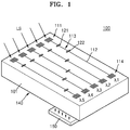
- FIG. 1 is a schematic perspective view of a spectrometer according to an exemplary embodiment.
- the spectrometer 100 may include a coupler device 140 based on silicon photonics and a photodetector 150.
- the coupler device 140 may receive a scattered light LS from an object, divide the scattered light LS according to wavelengths, and provide the divided lights to the photodetector 150.
- the photodetector 150 may detect the intensities of a plurality of light beams divided by the coupler device 140 according to wavelengths.
- the photodetector 150 may include a charge coupled device (CCD) image sensor, a complementary metal oxide semiconductor (CMOS) image sensor, or an array of photosensors.
- the spectrometer 100 may analyze a spectrum distribution of the scattered light LS in relevant wavelength bands.
- CCD charge coupled device
- CMOS complementary metal oxide semiconductor
- the coupler device 140 may include an input coupler 111 configured to couple an incident light to the coupler device 140, a waveguide 112 along which the light coupled by the input coupler 111 propagates, a resonator 113 configured to resonate the light coupled by the input coupler 111, and an output coupler 114 configured to output the light resonated by the resonator 113 to the photodetector 150.
- the resonator 113 may include two resonator mirrors 121 and 122 disposed in the waveguide 112. In this structure, the light coupled by the input coupler 111 may propagate along the waveguide 112.
- the light may resonate between the two resonator mirrors 121 and 122 of the resonator 113, and only the light having a resonance wavelength of the resonator 113 may be output from the resonator 113.
- the light output from the resonator 113 may propagate from the coupler device 140 to the photodetector 150 through the output coupler 114.
- the coupler device 140 may include at least two input couplers 111, at least two waveguides 112, at least two resonators 113, and at least two output couplers 114.
- the input couplers 111 may be configured to respectively couple lights of different wavelengths.
- one of the input couplers 111 may be configured to selectively couple a light of a first wavelength band ⁇ 1
- another of the input couplers 111 may be configured to selectively couple a light of a second wavelength band ⁇ 2.
- the resonators 113 may be configured to respectively resonate lights of different wavelengths.
- one of the resonators 113 may be configured to resonate a light of the first wavelength band ⁇ 1, and another of the resonators 113 may be configured to resonate a light of the second wavelength band ⁇ 2.
- the resonance wavelength of the resonator 113 may be adjusted by the distance between the two resonator mirrors 121 and 122.
- the resonator 113 may be optically connected to any one of the input couplers 111 and resonate the light of substantially the same wavelength band as the selective wavelength band of the input coupler 111 connected thereto.
- the input coupler 111 configured to selectively couple the light of the first wavelength band ⁇ 1 may be optically connected to the resonator 113 having a resonance wavelength of the first wavelength band ⁇ 1.
- the input couplers 111, the waveguides 112, the resonators 113, and the output couplers 114 may be disposed in parallel to each other at different positions in the widthwise direction of the coupler device 140.
- the lights of different wavelengths may be incident on the photodetector 150 respectively from the output couplers 114 disposed at the different positions in the widthwise direction of the coupler device 140. Then, the lights of different wavelengths may be respectively incident on different positions of the photodetector 150.
- a spectrum distribution of the incident light may be analyzed by measuring the intensities of lights respectively incident on the different positions of the photodetector 150.
- FIG. 1 exemplarily illustrates five input couplers 111, five waveguides 112, five resonators 113, and five output couplers 114.
- the spectrometer 100 may divide the incident light into five wavelength bands ⁇ 1, ⁇ 2, ⁇ 3, ⁇ 4, and ⁇ 5.
- the number of input couplers 111, waveguides 112, resonators 113, or output couplers 114 illustrated in FIG. 1 is merely exemplary.
- ten or more input couplers 111, waveguides 112, resonators 113, and output couplers 114 may be disposed to analyze desired biometric information on the basis of biometric optical signals transmitted or scattered from a living body.
- FIG. 1 illustrates that the input coupler 111, the resonator 113, and the output coupler 114 are physically connected through one waveguide 112, this is merely exemplary. That is, the input coupler 111, the resonator 113, and the output coupler 114 may not be physically connected through one waveguide 112, and any means may be used to transmit the light from the input coupler 111 to the resonator 113 and transmit the light from the resonator 113 to the output coupler 114. For example, an empty space may exist between the resonator 113 and the output coupler 114, and the waveguide 112 may exist only partially therein.
- FIG. 2 is a schematic perspective view of a spectrometer according to another exemplary embodiment.
- the spectrometer 200 illustrated in FIG. 2 may include a single input coupler 111 and a single output coupler 114.
- the input coupler 111 and output coupler 114 may be optically connected to at least two waveguides 112 and at least two resonators 113.
- the input coupler 111 and the output coupler 114 may not have a wavelength selectivity.
- the input coupler 111 may couple lights of all wavelength bands and provide the coupled lights to waveguides 112 respectively.
- the resonators 113 having different resonance wavelengths respectively may output only the lights of the respective wavelengths to the output coupler 114.
- FIG. 2 illustrates that the spectrometer 200 includes one input coupler 111 and one output coupler 114
- at least two input couplers 111 having a wavelength selectivity and one output coupler 114 not having a wavelength selectivity may be included according to another exemplary embodiment.
- one input coupler 111 not having a wavelength selectivity and at least two output couplers 114 having a wavelength selectivity may be included according to another exemplary embodiment.
- the input coupler 111 includes a grating-type coupler having a periodic grating structure, and the grating-type coupler has a polarization selectivity.
- the input coupler 111 may couple either a p-polarization component (also referred to as transverse-magnetic (TM) component) or an s-polarization component (also referred to as transverse-electric (TE) component) of light incident onto the input coupler 111.
- TM transverse-magnetic
- TE transverse-electric
- the coupler device 140 according to the present exemplary embodiment may be configured to have a two-layer structure having a selectivity with respect to the p-polarization component and the s-polarization component to improve the coupling efficiency by coupling the lights of all polarization components.
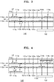
- FIG. 3 is a schematic cross-sectional view of a coupler device according to an exemplary embodiment.
- the coupler device 140 may include a first coupler layer 110a and a second coupler layer 110b.
- the coupler device 140 may further include a transparent dielectric layer 101 in which the first coupler layer 110a and the second coupler layer 110b are buried.
- the first coupler layer 110a and the second coupler layer 110b may be fixed and disposed respectively in different layers by the transparent dielectric layer 101.
- the first coupler layer 110a and the second coupler layer 110b may include a material having a higher refractive index than the transparent dielectric layer 101 therearound.
- the transparent dielectric layer 101 may include SiO 2 or siloxane-based spin-on glass (SOG), and the first coupler layer 110a and the second coupler layer 110b may include a high-refractive index material such as TiO 2 , SiN 3 , ZnS, ZnSe, or Si 3 N 4 .
- the first coupler layer 110a and the second coupler layer 110b may include the same material or may include different materials to improve the wavelength selectivity.
- the first coupler layer 110a and the second coupler layer 110b may be disposed respectively in different layers along an incident light propagation direction in the transparent dielectric layer 101.
- the first coupler layer 110a and the second coupler layer 110b may have opposite polarization selectivities.
- the first coupler layer 110a may be configured to have a selectivity with respect to the light of the p-polarization component
- the second coupler layer 110b may be configured to have a selectivity with respect to the light of the s-polarization component.
- the coupler device 140 may be a dual coupler device having a dual-layer structure.
- the first coupler layer 110a may include a first input coupler 111 a, a first waveguide 112a, a first resonator 113a, and a first output coupler 114a that are disposed in the same layer.
- the first coupler layer 110a may include at least two first input couplers 111 a, at least two first waveguides 112a, at least two first resonators 113a, and at least two first output couplers 114a, which have different wavelength selectivities.
- each of the first resonators 113a may include two resonator mirrors 121 a and 122a that are disposed in the first waveguide 112a.
- the first input coupler 111 a may be, for example, a grating-type coupler having a periodic grating structure configured to have a selectivity with respect to the light of the p-polarization component.
- the light of the p-polarization component among the incident lights may be provided to the first waveguide 112a through the first input coupler 111 a.
- the second coupler layer 110b may include a second input coupler 111 b, a second waveguide 112b, a second resonator 113b, and a second output coupler 114b that are disposed in the same layer.
- the second coupler layer 110b may include at least two second input couplers 111 b, at least two second waveguides 112b, at least two second resonators 113b, and at least two second output couplers 114b, which have different wavelength selectivities.
- Each of the second resonators 113b may include two resonator mirrors 121b and 122b that are disposed in the second waveguide 112b.
- the second input coupler 111 b may be, for example, a grating-type coupler having a periodic grating structure configured to have a selectivity with respect to the light of the s-polarization component.
- the light of the s-polarization component among the incident lights may be provided to the second waveguide 112b through the second input coupler 111 b.
- the first coupler layer 110a and the second coupler layer 110b may be disposed in different layers to be parallel to and face each other.
- the first input coupler 111a, the first waveguide 112a, the first resonator 113a, and the first output coupler 114a of the first coupler layer 110a may be arranged in parallel to the second input coupler 111b, the second waveguide 112b, the second resonator 113b, and the second output coupler 114b of the second coupler layer 110b.
- the at least two first input couplers 111 a, the at least two first waveguides 112a, and the at least two first resonators 113a of the first coupler layer 110a arranged in the widthwise direction of the coupler device 140 may be disposed to face the at least two second input couplers 111 b, the at least two second waveguides 112b, and the at least two second resonators 113b of the second coupler layer 110b, respectively.
- the two elements appear to overlap with each other when viewed in a height wise direction, that is, the vertical direction of the top surface of the transparent dielectric layer 101.
- the first and second input couplers 111 a and 111 b disposed to face each other may be configured to have different polarization selectivities with respect to the same wavelength band.
- the first input coupler 111 a configured to selectively couple the light of the first wavelength band ⁇ 1 having the p-polarization component may be disposed to face the second input coupler 111b configured to selectively couple the light of the first wavelength band ⁇ 1 having the s-polarization component.
- the wavelength bands of the lights coupled respectively by the first input coupler 111a and the second input coupler 111b facing each other may not necessarily be identical to each other.
- the wavelength band of the light coupled by the first input coupler 111 a may overlap partially with the wavelength band of the light coupled by the second input coupler 111b facing the first input coupler 111 a.
- the wavelength band of the light coupled by the first input coupler 111 a may be ⁇ 1 ⁇ ⁇
- the wavelength band of the light coupled by the second input coupler 111 b facing the first input coupler 111 a may be ⁇ 1 ⁇ ⁇ '.
- the first and second resonators 113a and 113b disposed to face each other may be configured to have substantially the same resonance wavelength.
- the first resonator 113a configured to resonate the light of the first wavelength band ⁇ 1 may be disposed to face the second resonator 113b configured to resonate the light of the first wavelength band ⁇ 1.
- the distance between the two resonator mirrors 121 a and 122a and the distance between the two resonator mirrors 121 b and 122b in the first and second resonators 113a and 113b disposed to face each other may be equal to each other.
- the first and second output couplers 114a and 114b may be disposed respectively at positions that do not overlap with each other in a lengthwise direction, that is, the light propagation direction in the first and second waveguides 112a and 112b. This is done so that the light output from the first output coupler 114a and propagating toward the photodetector 150 may not pass through the second output coupler 114b. Thus, the light propagating from the first output coupler 114a toward the photodetector 150 may reach the photodetector 150 without being obstructed by the second output coupler 114b.
- the coupler device 140 illustrated in FIG. 3 may be applied to the spectrometer 100 illustrated in FIG. 1 and also to the spectrometer 200 illustrated in FIG. 2 .
- the coupler device 140 illustrated in FIG. 3 may be applied to the spectrometer 100 illustrated in FIG. 1 and also to the spectrometer 200 illustrated in FIG. 2 .
- only one first input coupler 111 a may be optically connected to the at least two first waveguides 112a and the at least two first resonators 113a.
- only one second input coupler 111 b may be optically connected to the at least two second waveguides 112b and the at least two second resonators 113b.
- the coupling efficiency of the coupler device 140 may be improved by using the first coupler layer 110a and the second coupler layer 110b operating independently of each other as described above.
- the first coupler layer 110a may be designed to optimize the reception of the light of the p-polarization component
- the second coupler layer 110b may be designed to optimize the reception of the light of the s-polarization component.
- the coupler device 140 may receive both the light of the p-polarization component and the light of the s-polarization component, which are included in the incident lights, with high efficiency. Consequently, the spectrum analysis accuracy of the spectrometers 100 and 200 including the coupler device 140 may be improved.
- the first coupler layer 110a and the second coupler layer 110b may be arranged in different-height layers without increasing the area of the coupler device 140.
- the spectrometers 100 and 200 including the coupler device 140 may be miniaturized.
- FIG. 4 is a schematic cross-sectional view of a coupler device according to another exemplary embodiment.
- the coupler device 140 may further include a first reflector 131 and a second reflector 132.
- the first reflector 131 may be disposed to face the first and second input couplers 111 a and 111 b
- the second reflector 132 may be disposed to face the first and second output couplers 114a and 114b.
- the first reflector 131 is configured to reflect light, which passes through the first and second input couplers 111 a and 111 b without being absorbed by the first and second input couplers 111 a and 111 b, to the first and second input couplers 111 a and 111 b.
- the first reflector 131 may receive the light bouncing off the first reflector 131.
- the coupling efficiency of the coupler device 140 may be further improved by reusing the light that remains without being absorbed.
- the first reflector 131 may be disposed on an opposite side to a light incident surface of the coupler device 140 on which the light is incident. For example, when the light is incident on the top surface of the coupler device 140, the first reflector 131 may be disposed between the bottom surface of the coupler device 140 and the second input coupler 111b.
- the coupling efficiency of the first and second input couplers 111 a and 111b may be further improved by using the fact that a phase difference occurs between the reflected light of the p-polarization component and the reflected light of the s-polarization component when the light is incident on the first reflector 131 at an angle smaller than the Brewster's angle.
- the phase difference between the reflected light of the p-polarization component and the reflected light of the s-polarization component is 180°, and the same effect may be achieved also in a dielectric Bragg reflector.
- the distance between the first input coupler 111 a and the first reflector 131 may be set to cause a destructive interference between the incident light and the reflected light with respect to the light of the s-polarization component and a constructive interference between the incident light and the reflected light with respect to the light of the p-polarization component in the first input coupler 111 a. Then, the selectivity of the light of the p-polarization component in the first input coupler 111 a may be further improved.
- the distance between the second input coupler 111 b and the first reflector 131 may be set to cause a destructive interference between the incident light and the reflected light with respect to the light of the p-polarization component and a constructive interference between the incident light and the reflected light with respect to the light of the s-polarization component in the second input coupler 111 b. Then, the selectivity of the light of the s-polarization component in the second input coupler 111 b may be further improved.
- FDTD finite-difference in time-domain
- the first reflector 131 when the first reflector 131 is disposed, about 60% of the light of the p-polarization component is absorbed by the first input coupler 111 a and about 1 % of the light of the p-polarization component is absorbed by the second input coupler 111 b. Also, about 2% of the light of the s-polarization component is absorbed by the first input coupler 111 a and about 50% of the light of the s-polarization component is absorbed by the second input coupler 111b. Thus, the signal-to-noise ratio and the coupling efficiency of the coupler device 140 may be greatly improved.
- the second reflector 132 is configured to reflect the light, which is scattered without propagating from the first and second output couplers 114a and 114b, to the photodetector 150.
- the output coupling efficiency may be improved by increasing the amount of light output to the photodetector 150 by using the second reflector 132.
- the second reflector 132 may be disposed on an opposite side to the photodetector 150. For example, when the photodetector 150 is disposed to face the bottom surface of the coupler device 140, the second reflector 132 may be disposed between the top surface of the coupler device 140 and the first input coupler 111 a.
- the spectrometers 100 and 200 may be manufactured to be micro-sized in the form of a semiconductor chip while having high resolution and accuracy. Thus, a non-invasive biometric sensor installed in a mobile apparatus may be implemented by using the above spectrometers 100 and 200.
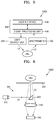
- FIG. 5 is a schematic block diagram of a non-invasive biometric sensor including the spectrometer of FIG. 1 according to an exemplary embodiment.
- the non-invasive biometric sensor 1000 may include a light source unit (e.g., light emitter) 300 configured to radiate an excitation light LE to an object OBJ, and a spectrometer 100 configured to spectroscope a scattered light LS generated from the object OBJ.
- the object OBJ may include a human body, a living body of an animal, or a food.
- the object OBJ may be a human body for blood sugar measurement or a food for freshness measurement, and may be a sample for analysis of air pollution or water pollution.
- the light source unit 300 may include a light source and may also include at least one optical member for guiding the light from the light source to a desired position of the object OBJ.
- the light source may be configured to radiate a light of a wavelength band predetermined based on an analysis target property of the object OBJ.
- the light source may radiate a near-infrared light of a wavelength band of about 0.8 ⁇ m to about 2.5 ⁇ m.
- the light source may include, for example, a light-emitting diode (LED) or a laser diode (LD).
- the non-invasive biometric sensor 1000 may further include a control unit (e.g., a controller or hardware computing device) 600 configured to analyze the properties of the object OBJ on the basis of signals sensed by the spectrometer 100 and generate corresponding control signals.
- the control unit 600 may include a user interface 500 and a signal processing unit (e.g., signal processor) 400.
- the user interface unit 500 may include an input unit and a display.
- the signal processing unit 400 may analyze the properties of the object OBJ on the basis of the signals sensed by the spectrometer 100.
- the signal processing unit 400 may analyze the properties of the object OBJ by Raman spectroscopy or near-infrared (NIR) absorption spectrum analysis.
- NIR near-infrared
- the Raman spectroscopy may use scattering (particularly inelastic scattering) in which the light input into the object OBJ is scattered in various directions by colliding with molecules or atoms included in the object OBJ.
- the incident light is emitted after being absorbed into molecules or atoms, wherein the scattered light may have a longer wavelength than the incident light and a wavelength difference between the scattered light and the incident light may be about 200 nm or less.
- Various properties, such as the structure of molecules and the vibration of molecules in the object OBJ may be detected by analyzing the spectrum of the scattered light.
- the signal processing unit 400 may process the analysis result into a video signal to be displayed on the display of the user interface 500. Also, the signal processing unit 400 may transmit a control signal to the light source unit 300 according to the input from the user interface 500.
- the signal processing unit 400 may be implemented by a microprocessor.
- the spectrometer 100 and the control unit 600 may be connected to each other via wire or wireless communication.
- the non-invasive biometric sensor 1000 may be implemented as a mini portable device in which the spectrometer 100 and the control unit 600 are connected by wire.
- the control unit 600 may be mounted on a portable mobile communication device to wirelessly communicate with the spectrometer 100.
- FIG. 6 illustrates an example of an optical arrangement of the non-invasive biometric sensor 1000 illustrated in FIG. 5 .
- the non-invasive biometric sensor 1000 may be implemented as a reflection type.
- An optical system of the non-invasive biometric sensor 1000 may be configured such that the spectrometer 100 may sense the scattered light LS reflected from the object OBJ.
- the light source unit 300 may include a light source 310, a light path converter 320, and a diaphragm 330.
- the light path converter 320 is illustrated as being a prism type, this is merely exemplary and the light path converter 320 may also be a beam splitter type or a flat mirror type.
- the light path converter 320 may be omitted according to the position of the light source 310.
- the light source unit 300 may further include an optical lens 350 configured to focus the scattered light LS from the object OBJ on the spectrometer 100.
- the excitation light LE radiated from the light source 310 collides with a molecular structure in the object OBJ.
- the excitation light is absorbed into the molecular structure and emitted therefrom so that a wavelength-converted scattered light LS is output from the object OBJ.
- the scattered light LS that is, a biometric optical signal may include various spectrums having different wavelength conversion degrees according to the molecular states in the object OBJ.
- the non-invasive biometric sensor 1000 includes an optical system structure in which the scattered light LS output along the same path as the input path of the excitation light LE to the object OBJ is input to the spectrometer 100. Also, the non-invasive biometric sensor 1000 may further include an additional optical device that branches the scattered light LS to the spectrometer 100.
- FIG. 7 illustrates another example of the optical arrangement of the non-invasive biometric sensor 1000 illustrated in FIG. 5 .
- the non-invasive biometric sensor 1000 may be implemented as a transmission type.
- An optical system of the non-invasive biometric sensor 1000 may be configured such that the spectrometer 100 may sense the scattered light LS transmitted through the object OBJ.
- the light source unit 300 may include a light source 310, a light path converter 320, and a diaphragm 330.
- the light path converter 320 is illustrated as being a prism type, this is merely exemplary and the light path converter 320 may also be a beam splitter type or a flat mirror type.
- the light path converter 320 may be omitted according to the position of the light source 310.
- the light source unit 300 may further include an optical lens 350 configured to focus the scattered light LS from the object OBJ on the spectrometer 100.
- the excitation light LE radiated from the light source 310 collides with a molecular structure in the object OBJ.
- the excitation light LE is absorbed into the molecular structure and emitted therefrom so that a wavelength-converted scattered light LS is output from the object OBJ.
- the scattered light LS that is, a biometric optical signal may include various spectrums having different wavelength conversion degrees according to the molecular states in the object OBJ.
- the non-invasive biometric sensor 1000 includes an optical system structure in which the scattered light LS output through the object OBJ is input to the spectrometer 100.
- FIG. 8 illustrates another example of the optical arrangement of the non-invasive biometric sensor 1000 illustrated in FIG. 5 .
- the non-invasive biometric sensor 1000 may further include a base 380, and the light source 310 and the spectrometer 100 may be disposed on the same surface of the base 380 or on different surfaces of the base 380.
- the base 380 may be formed of a transparent material, and the light source 310 and the spectrometer 100 may be disposed on the same surface of the base 380 while being spaced apart from each other.
- the light source 310 may be disposed to radiate the excitation light LE to the object OBJ through the base 380.
- the spectrometer 100 may be disposed to sense the scattered light LS that is input from the object OBJ through the base 380. Also, on the other surface of the base 380, an optical lens 360 may be further disposed to focus the excitation light LE from the light source 310 on the object OBJ and focus the scattered light LS from the object OBJ on the spectrometer 100.
- the base 380 may be formed of a flexible material.
- the non-invasive biometric sensor 1000 may be configured to be wearable on the object OBJ.
- the non-invasive biometric sensor 1000 may be implemented as an armlet-type non-invasive blood sugar sensor.
- the control unit 600 may be disposed on the base 380 together with the spectrometer 100.
- the non-invasive biometric sensor 1000 may be implemented in such a manner that only the light source 310 and the spectrometer 100 are formed in an armlet-type wearable structure and the control unit 600 is mounted on a mobile device.
Landscapes
- Physics & Mathematics (AREA)
- Spectroscopy & Molecular Physics (AREA)
- Health & Medical Sciences (AREA)
- Life Sciences & Earth Sciences (AREA)
- General Physics & Mathematics (AREA)
- General Health & Medical Sciences (AREA)
- Pathology (AREA)
- Engineering & Computer Science (AREA)
- Biomedical Technology (AREA)
- Heart & Thoracic Surgery (AREA)
- Medical Informatics (AREA)
- Molecular Biology (AREA)
- Surgery (AREA)
- Animal Behavior & Ethology (AREA)
- Biophysics (AREA)
- Public Health (AREA)
- Veterinary Medicine (AREA)
- Optics & Photonics (AREA)
- Chemical & Material Sciences (AREA)
- Analytical Chemistry (AREA)
- Biochemistry (AREA)
- Immunology (AREA)
- Emergency Medicine (AREA)
- Microelectronics & Electronic Packaging (AREA)
- Mathematical Physics (AREA)
- Theoretical Computer Science (AREA)
- Nuclear Medicine, Radiotherapy & Molecular Imaging (AREA)
- Investigating Or Analysing Materials By Optical Means (AREA)
- Measurement Of The Respiration, Hearing Ability, Form, And Blood Characteristics Of Living Organisms (AREA)
Abstract
Description
- Apparatuses and methods consistent with exemplary embodiments relate to dual coupler devices configured to receive lights of different polarization components, spectrometers including the dual coupler devices, and non-invasive biometric sensors including the spectrometers.
- A non-invasive blood sugar measurement may be performed through spectroscopic analysis of a biometric signal that is obtained when incident light is reflected off the skin of a human subject. With improvements in performance of mobile apparatuses such as mobile phones, integrating a non-invasive biometric sensor into a mobile apparatus may be attempted. To this end, a micro spectrometer may be installed in a mobile apparatus.
- For example, the micro spectrometer may be implemented as a linear variable filter (LVF)-based spectrometer or a filter array-based spectrometer. The LVF-based spectrometer may have a structure in which a spacer having a gradually changing thickness is disposed on a plurality of photodiode pixels so that the thickness of the LVF-based spectrometer varies continuously or in steps. Respective photodiode pixels in the LVF-based spectrometer may sense lights of different wavelength bands because a transmission wavelength varies depending on the thickness of the spacer. The filter array-based spectrometer may have a structure in which bandpass filters (BPFs) of different transmission bands are disposed in respective photodiode pixels.
- One or more exemplary embodiments provide dual coupler devices that are used in silicon photonics-based spectrometers and are configured to receive lights of different polarization components.
- Further, one or more exemplary embodiments provide spectrometers including the dual coupler devices.
- Further still, one or more exemplary embodiments provide non-invasive biometric sensors including the spectrometers.
- According to an aspect of an exemplary embodiment, there is provided a dual coupler device including: a first coupler layer configured to receive a light of a first polarization component among incident lights; and a second coupler layer configured to receive a light of a second polarization component among the incident lights, wherein a polarization direction of the light of the first polarization component is perpendicular to a polarization direction of the light of the second polarization component, and the first coupler layer and the second coupler layer are spaced apart from each other and extended along a direction in which the incident lights propagate in the first coupler layer and the second coupler layer.
- Thus, there may be provided a polarization-independent coupler structure that may be of particular benefit to the field of miniaturized spectrometers, for example. Embodiments may propose a photonics chip structure having two kinds of light signal transmission circuits (or couplers) that are positioned or stacked (e.g. vertically layered) one above the other. By way of example, a first layer of the two-layer structure may be adapted for the TE-polarization mode and the other, second layer may be for the TM-polarization mode. Since light signal coupling for each layer is performed independently, the first layer can be optimized to the TE-polarization eigenmode, and the other, second layer may be optimized to the TM-polarization eigenmode. By utilizing such a structure, collected Raman signals may be transmitted efficiently to a photonics chip, for example.
- Proposed may be a technology capable of implementing a subminiature chip wherein one layer is optimized for one eigenmode of first kind of polarization and wherein another layer is optimized for one eigenmode of second, different kind of polarization, Such proposal embodiments may be able to receive any of the polarization signal within a small structure.
- The first coupler layer and the second coupler layer may be parallel to each other. Also, the first coupler layer and the second coupler layer may be disposed to face each other.
- The dual coupler device may further include a transparent dielectric layer in which the first coupler layer and the second coupler layer may be buried.
- The first coupler layer and the second coupler layer may have a higher refractive index than the transparent dielectric layer.
- The first coupler layer and the second coupler layer may each include a grating-type coupler having a periodic grating structure.
- The periodic grating structure of the first coupler layer may be configured to have selectivity with respect to the light of the first polarization component, and the periodic grating structure of the second coupler layer may be configured to have selectivity with respect to the light of the second polarization component.
- The periodic grating structure of the first coupler layer may be configured to have selectivity with respect to a light of a first wavelength band, and the periodic grating structure of the second coupler layer may be configured to have selectivity with respect to a light of a second wavelength band that overlaps at least partially with the first wavelength band.
- Herein, the first wavelength band and the second wavelength band may be substantially identical to each other.
- The dual coupler device may further include a reflector configured to reflect light, which passes through the first coupler layer and the second coupler layer among the incident lights, towards the first coupler layer and the second coupler layer.
- The reflector may be disposed apart from the first coupler layer by a first distance that creates destructive interference with the light of the second polarization component and constructive interference with the light of the first polarization component in the first coupler layer. Thus, a mirror may be employed in a bottom or lower layer of the coupler so as to reflect the light to the first and second coupler layers. By adjusting a distance between the coupler(s) and the mirror, constructive interference between the incident light and the reflected light by the mirror can be promoted, and thus it may be possible to improve coupling efficiency. Also, due to phase change characteristics of the reflector, selectivity between the first and second polarization component for each layer may be enhanced.
- The reflector may be disposed apart from the second coupler layer by a second distance that creates destructive interference with the light of the first polarization component and constructive interference with the light of the second polarization component in the second coupler layer.
- According to an aspect of another exemplary embodiment, there is provided a spectrometer including: a first coupler layer configured to receive a light of a first polarization component among incident lights; a second coupler layer configured to receive a light of a second polarization component among the incident lights; and a photodetector configured to detect the light received by each of the first coupler layer and the second coupler layer, wherein a polarization direction of the light of the first polarization component is perpendicular to a polarization direction of the light of the second polarization component, and the first coupler layer and the second coupler layer are spaced apart from each other and extended along a direction in which the incident lights propagate in the first coupler layer and the second coupler layer. Herein, the first coupler layer may include: a first input coupler configured to selectively couple the light of the first polarization component; a first waveguide along which the light of the first polarization component coupled by the first input coupler propagates; a first resonator configured to resonate the light of the first polarization component coupled by the first input coupler; and a first output coupler configured to output the light of the first polarization component resonated by the first resonator to the photodetector.
- Also, the second coupler layer may include: a second input coupler configured to selectively couple the light of the second polarization component; a second waveguide along which the light of the second polarization component coupled by the second input coupler propagates; a second resonator configured to resonate the light of the second polarization component coupled by the second input coupler; and a second output coupler configured to output the light of the second polarization component resonated by the second resonator to the photodetector.
- The first coupler layer may include at least two first resonators configured to resonate lights of different wavelengths respectively, and the second coupler layer may include at least two second resonators configured to resonate lights of different wavelengths respectively.
- One of the at least two first resonators of the first coupler layer and one of the at least two second resonators of the second coupler layer may be configured to resonate lights of substantially the same wavelength.
- The first resonator of the first coupler layer and the second resonator of the second coupler layer configured to resonate lights of the same wavelength may be disposed to face each other.
- The first coupler layer may include at least two first input couplers configured to selectively couple lights of different wavelengths respectively, and the second coupler layer may include at least two second input couplers configured to selectively couple lights of different wavelengths respectively.
- The first input coupler may be optically connected to the at least two first resonators, and the second input coupler may be optically connected to the at least two second resonators.
- The first coupler layer may include at least two first waveguides optically connected to the at least two first resonators respectively, and the second coupler layer may include at least two second waveguides optically connected to the at least two second resonators respectively.
- The first output coupler and the second output coupler may be disposed respectively at positions that do not overlap with each other in a light propagation direction in the first waveguide and the second waveguide.
- The spectrometer may further include a first reflector disposed to face the first input coupler and the second input coupler and configured to reflect light, which passes through the first coupler layer and the second coupler layer among the incident lights, towards the first coupler layer and the second coupler layer.
- The first reflector may be disposed apart from the first coupler layer by a first distance that creates destructive interference with the light of the second polarization component and constructive interference with the light of the first polarization component in the first input coupler.
- Also, the first reflector is disposed apart from the second coupler layer by a second distance that creates destructive interference with the light of the first polarization component and constructive interference with the light of the second polarization component in the second input coupler.
- Also, the spectrometer may further include a second reflector disposed to face the first output coupler and the second output coupler and configured to reflect the light, which is output from the first output coupler and the second output coupler, to the photodetector.
- According to an aspect of another exemplary embodiment, there is provided a non-invasive biometric sensor including: a light source configured to radiate an excitation light to an object; and a spectrometer configured to measure a spectrum distribution of a scattered light generated from the object by the excitation light. The spectrometer may include a first coupler layer configured to receive a light of a first polarization component among incident lights; a second coupler layer configured to receive a light of a second polarization component among the incident lights; and a photodetector configured to detect the light received by each of the first coupler layer and the second coupler layer, wherein a polarization direction of the light of the first polarization component is perpendicular to a polarization direction of the light of the second polarization component, and the first coupler layer and the second coupler layer are spaced apart from each other and extended along a direction in which the incident lights propagate in the first coupler layer and the second coupler layer. According to an aspect of another exemplary embodiment, there is provided a spectrometer including: a first coupler layer configured to receive light of a p-polarization component through a first input coupler; a second coupler layer that is configured to receive light of a s-polarization component through a second input coupler and disposed to be apart from the first coupler layer in a first direction perpendicular to a second direction in which the light of the p-polarization component and the light of the s-polarization component propagate in the first coupler layer and the second coupler layer, respectively; and a reflector that is disposed to be apart from the first coupler layer and the second coupler layer in the first direction, aligned with the first input coupler and the second input coupler in the second direction, and configured to bounce off light incident from the first coupler input and the second input coupler back to the first input coupler and the second input coupler.
- The first coupler layer may propagate the light of the p-polarization component towards a first output coupler disposed on the first coupler layer, the second coupler layer may propagate the light of the s-polarization component towards a second output coupler disposed on the second coupler layer, and the first output coupler may be disposed out of alignment with the second output coupler in the second direction.
- The spectrometer of may further include another reflector that is disposed to be apart from the first coupler layer and the second coupler layer in the first direction and is aligned to bounce off light incident from the first output coupler and the second output coupler back to the first output coupler and the second output coupler.
- The above and/or other aspects will be more apparent by describing certain exemplary embodiments, with reference to the accompanying drawings, in which:
-
FIG. 1 is a schematic perspective view of a spectrometer according to an exemplary embodiment; -
FIG. 2 is a schematic perspective view of a spectrometer according to another exemplary embodiment; -
FIG. 3 is a schematic cross-sectional view of a coupler device according to an exemplary embodiment; -
FIG. 4 is a schematic cross-sectional view of a coupler device according to another exemplary embodiment; -
FIG. 5 is a schematic block diagram of a non-invasive biometric sensor according to an exemplary embodiment; -
FIG. 6 illustrates an example of an optical arrangement of the non-invasive biometric sensor illustrated inFIG. 5 ; -
FIG. 7 illustrates another example of the optical arrangement of the non-invasive biometric sensor illustrated inFIG. 5 ; and -
FIG. 8 illustrates another example of the optical arrangement of the non-invasive biometric sensor illustrated inFIG. 5 . - Exemplary embodiments are described in greater detail below with reference to the accompanying drawings.
- In the following description, like drawing reference numerals are used for like elements, even in different drawings. The matters defined in the description, such as detailed construction and elements, are provided to assist in a comprehensive understanding of the exemplary embodiments. However, it is apparent that the exemplary embodiments can be practiced without those specifically defined matters. Also, well-known functions or constructions are not described in detail since they would obscure the description with unnecessary detail.
- As used herein, the term "and/or" includes any and all combinations of one or more of the associated listed items. Expressions such as "at least one of," when preceding a list of elements, modify the entire list of elements and do not modify the individual elements of the list.
- Hereinafter, dual coupler devices, spectrometers including the dual coupler devices, and non-invasive biometric sensors including the spectrometers according to exemplary embodiments will be described in detail with reference to the accompanying drawings. In the drawings, the sizes of elements may be exaggerated for clarity and convenience of description. It will be understood that when a layer is referred to as being "on" another layer, it may be directly on the other layer, or one or more intervening layers may also be present.
-
FIG. 1 is a schematic perspective view of a spectrometer according to an exemplary embodiment. Referring toFIG. 1 , thespectrometer 100 may include acoupler device 140 based on silicon photonics and aphotodetector 150. For example, thecoupler device 140 may receive a scattered light LS from an object, divide the scattered light LS according to wavelengths, and provide the divided lights to thephotodetector 150. Thephotodetector 150 may detect the intensities of a plurality of light beams divided by thecoupler device 140 according to wavelengths. For example, thephotodetector 150 may include a charge coupled device (CCD) image sensor, a complementary metal oxide semiconductor (CMOS) image sensor, or an array of photosensors. Thespectrometer 100 may analyze a spectrum distribution of the scattered light LS in relevant wavelength bands. - The
coupler device 140 may include aninput coupler 111 configured to couple an incident light to thecoupler device 140, awaveguide 112 along which the light coupled by theinput coupler 111 propagates, aresonator 113 configured to resonate the light coupled by theinput coupler 111, and anoutput coupler 114 configured to output the light resonated by theresonator 113 to thephotodetector 150. Theresonator 113 may include two resonator mirrors 121 and 122 disposed in thewaveguide 112. In this structure, the light coupled by theinput coupler 111 may propagate along thewaveguide 112. Also, the light may resonate between the two resonator mirrors 121 and 122 of theresonator 113, and only the light having a resonance wavelength of theresonator 113 may be output from theresonator 113. The light output from theresonator 113 may propagate from thecoupler device 140 to thephotodetector 150 through theoutput coupler 114. - In order to divide the incident light according to wavelengths, the
coupler device 140 may include at least twoinput couplers 111, at least twowaveguides 112, at least tworesonators 113, and at least twooutput couplers 114. Theinput couplers 111 may be configured to respectively couple lights of different wavelengths. For example, one of theinput couplers 111 may be configured to selectively couple a light of a first wavelength band λ1, and another of theinput couplers 111 may be configured to selectively couple a light of a second wavelength band λ2. Also, theresonators 113 may be configured to respectively resonate lights of different wavelengths. For example, one of theresonators 113 may be configured to resonate a light of the first wavelength band λ1, and another of theresonators 113 may be configured to resonate a light of the second wavelength band λ2. The resonance wavelength of theresonator 113 may be adjusted by the distance between the two resonator mirrors 121 and 122. Theresonator 113 may be optically connected to any one of theinput couplers 111 and resonate the light of substantially the same wavelength band as the selective wavelength band of theinput coupler 111 connected thereto. For example, theinput coupler 111 configured to selectively couple the light of the first wavelength band λ1 may be optically connected to theresonator 113 having a resonance wavelength of the first wavelength band λ1. - As illustrated in
FIG. 1 , theinput couplers 111, thewaveguides 112, theresonators 113, and theoutput couplers 114 may be disposed in parallel to each other at different positions in the widthwise direction of thecoupler device 140. According to the present exemplary embodiment, the lights of different wavelengths may be incident on thephotodetector 150 respectively from theoutput couplers 114 disposed at the different positions in the widthwise direction of thecoupler device 140. Then, the lights of different wavelengths may be respectively incident on different positions of thephotodetector 150. Thus, a spectrum distribution of the incident light may be analyzed by measuring the intensities of lights respectively incident on the different positions of thephotodetector 150. -
FIG. 1 exemplarily illustrates fiveinput couplers 111, fivewaveguides 112, fiveresonators 113, and fiveoutput couplers 114. Thus, thespectrometer 100 may divide the incident light into five wavelength bands λ1, λ2, λ3, λ4, and λ5. However, the number ofinput couplers 111,waveguides 112,resonators 113, oroutput couplers 114 illustrated inFIG. 1 is merely exemplary. For example, ten ormore input couplers 111,waveguides 112,resonators 113, andoutput couplers 114 may be disposed to analyze desired biometric information on the basis of biometric optical signals transmitted or scattered from a living body. - Also, although
FIG. 1 illustrates that theinput coupler 111, theresonator 113, and theoutput coupler 114 are physically connected through onewaveguide 112, this is merely exemplary. That is, theinput coupler 111, theresonator 113, and theoutput coupler 114 may not be physically connected through onewaveguide 112, and any means may be used to transmit the light from theinput coupler 111 to theresonator 113 and transmit the light from theresonator 113 to theoutput coupler 114. For example, an empty space may exist between theresonator 113 and theoutput coupler 114, and thewaveguide 112 may exist only partially therein. Thus, theinput coupler 111, thewaveguide 112, theresonator 113, and theoutput coupler 114 may be optically connected although not physically connected. Also, a light path from theinput coupler 111 to theoutput coupler 114 may not necessarily be a straight line.FIG. 2 is a schematic perspective view of a spectrometer according to another exemplary embodiment. Thespectrometer 200 illustrated inFIG. 2 may include asingle input coupler 111 and asingle output coupler 114. Theinput coupler 111 andoutput coupler 114 may be optically connected to at least twowaveguides 112 and at least tworesonators 113. Other than the number of theinput coupler 111 and theoutput coupler 114, the configuration of thespectrometer 200 illustrated inFIG. 2 may be identical to the configuration of thespectrometer 100 illustrated inFIG. 1 . In the exemplary embodiment illustrated inFIG. 2 , theinput coupler 111 and theoutput coupler 114 may not have a wavelength selectivity. For example, theinput coupler 111 may couple lights of all wavelength bands and provide the coupled lights towaveguides 112 respectively. Also, theresonators 113 having different resonance wavelengths respectively may output only the lights of the respective wavelengths to theoutput coupler 114. - Also, although
FIG. 2 illustrates that thespectrometer 200 includes oneinput coupler 111 and oneoutput coupler 114, at least twoinput couplers 111 having a wavelength selectivity and oneoutput coupler 114 not having a wavelength selectivity may be included according to another exemplary embodiment. Also, oneinput coupler 111 not having a wavelength selectivity and at least twooutput couplers 114 having a wavelength selectivity may be included according to another exemplary embodiment. In general, theinput coupler 111 includes a grating-type coupler having a periodic grating structure, and the grating-type coupler has a polarization selectivity. For example, theinput coupler 111 may couple either a p-polarization component (also referred to as transverse-magnetic (TM) component) or an s-polarization component (also referred to as transverse-electric (TE) component) of light incident onto theinput coupler 111. When some polarization components of the incident light are not coupled, the coupling efficiency of the input coupler 11 may degrade and light loss may occur. In that case, stable spectrum analysis of the spectrometer may be difficult. Thecoupler device 140 according to the present exemplary embodiment may be configured to have a two-layer structure having a selectivity with respect to the p-polarization component and the s-polarization component to improve the coupling efficiency by coupling the lights of all polarization components. - For example,
FIG. 3 is a schematic cross-sectional view of a coupler device according to an exemplary embodiment. Referring toFIG. 3 , thecoupler device 140 may include afirst coupler layer 110a and asecond coupler layer 110b. Also, thecoupler device 140 may further include atransparent dielectric layer 101 in which thefirst coupler layer 110a and thesecond coupler layer 110b are buried. Thefirst coupler layer 110a and thesecond coupler layer 110b may be fixed and disposed respectively in different layers by thetransparent dielectric layer 101. Herein, thefirst coupler layer 110a and thesecond coupler layer 110b may include a material having a higher refractive index than thetransparent dielectric layer 101 therearound. For example, thetransparent dielectric layer 101 may include SiO2 or siloxane-based spin-on glass (SOG), and thefirst coupler layer 110a and thesecond coupler layer 110b may include a high-refractive index material such as TiO2, SiN3, ZnS, ZnSe, or Si3N4. Also, thefirst coupler layer 110a and thesecond coupler layer 110b may include the same material or may include different materials to improve the wavelength selectivity. - As illustrated in
FIG. 3 , thefirst coupler layer 110a and thesecond coupler layer 110b may be disposed respectively in different layers along an incident light propagation direction in thetransparent dielectric layer 101. Thefirst coupler layer 110a and thesecond coupler layer 110b may have opposite polarization selectivities. For example, thefirst coupler layer 110a may be configured to have a selectivity with respect to the light of the p-polarization component, and thesecond coupler layer 110b may be configured to have a selectivity with respect to the light of the s-polarization component. In this regard, thecoupler device 140 may be a dual coupler device having a dual-layer structure. - The
first coupler layer 110a may include afirst input coupler 111 a, afirst waveguide 112a, afirst resonator 113a, and afirst output coupler 114a that are disposed in the same layer. Although not illustrated inFIG. 3 , as illustrated inFIGS. 1 and2 , thefirst coupler layer 110a may include at least twofirst input couplers 111 a, at least twofirst waveguides 112a, at least twofirst resonators 113a, and at least twofirst output couplers 114a, which have different wavelength selectivities. Also, each of thefirst resonators 113a may include two resonator mirrors 121 a and 122a that are disposed in thefirst waveguide 112a. Herein, thefirst input coupler 111 a may be, for example, a grating-type coupler having a periodic grating structure configured to have a selectivity with respect to the light of the p-polarization component. Thus, the light of the p-polarization component among the incident lights may be provided to thefirst waveguide 112a through thefirst input coupler 111 a. - Also, the
second coupler layer 110b may include asecond input coupler 111 b, asecond waveguide 112b, asecond resonator 113b, and asecond output coupler 114b that are disposed in the same layer. Like thefirst coupler layer 110a, thesecond coupler layer 110b may include at least twosecond input couplers 111 b, at least twosecond waveguides 112b, at least twosecond resonators 113b, and at least twosecond output couplers 114b, which have different wavelength selectivities. Each of thesecond resonators 113b may include two resonator mirrors 121b and 122b that are disposed in thesecond waveguide 112b. Thesecond input coupler 111 b may be, for example, a grating-type coupler having a periodic grating structure configured to have a selectivity with respect to the light of the s-polarization component. Thus, the light of the s-polarization component among the incident lights may be provided to thesecond waveguide 112b through thesecond input coupler 111 b. - The
first coupler layer 110a and thesecond coupler layer 110b may be disposed in different layers to be parallel to and face each other. For example, thefirst input coupler 111a, thefirst waveguide 112a, thefirst resonator 113a, and thefirst output coupler 114a of thefirst coupler layer 110a may be arranged in parallel to thesecond input coupler 111b, thesecond waveguide 112b, thesecond resonator 113b, and thesecond output coupler 114b of thesecond coupler layer 110b. Also, the at least twofirst input couplers 111 a, the at least twofirst waveguides 112a, and the at least twofirst resonators 113a of thefirst coupler layer 110a arranged in the widthwise direction of thecoupler device 140 may be disposed to face the at least twosecond input couplers 111 b, the at least twosecond waveguides 112b, and the at least twosecond resonators 113b of thesecond coupler layer 110b, respectively. When two elements face each other, the two elements appear to overlap with each other when viewed in a height wise direction, that is, the vertical direction of the top surface of thetransparent dielectric layer 101. - The first and
second input couplers first input coupler 111 a configured to selectively couple the light of the first wavelength band λ1 having the p-polarization component may be disposed to face thesecond input coupler 111b configured to selectively couple the light of the first wavelength band λ1 having the s-polarization component. However, the wavelength bands of the lights coupled respectively by thefirst input coupler 111a and thesecond input coupler 111b facing each other may not necessarily be identical to each other. Instead, the wavelength band of the light coupled by thefirst input coupler 111 a may overlap partially with the wavelength band of the light coupled by thesecond input coupler 111b facing thefirst input coupler 111 a. For example, the wavelength band of the light coupled by thefirst input coupler 111 a may be λ1 ± Δλ, and the wavelength band of the light coupled by thesecond input coupler 111 b facing thefirst input coupler 111 a may be λ1 ± Δλ'. Likewise, the first andsecond resonators first resonator 113a configured to resonate the light of the first wavelength band λ1 may be disposed to face thesecond resonator 113b configured to resonate the light of the first wavelength band λ1. The distance between the two resonator mirrors 121 a and 122a and the distance between the two resonator mirrors 121 b and 122b in the first andsecond resonators - As illustrated in
FIG. 3 , the first andsecond output couplers second waveguides first output coupler 114a and propagating toward thephotodetector 150 may not pass through thesecond output coupler 114b. Thus, the light propagating from thefirst output coupler 114a toward thephotodetector 150 may reach thephotodetector 150 without being obstructed by thesecond output coupler 114b. - Although it has been described above that at least two
first input couplers 111 a, at least twosecond input couplers 111 b, at least twofirst output couplers 114a, and at least twosecond output couplers 114b are disposed, thecoupler device 140 illustrated inFIG. 3 may be applied to thespectrometer 100 illustrated inFIG. 1 and also to thespectrometer 200 illustrated inFIG. 2 . For example, only onefirst input coupler 111 a may be optically connected to the at least twofirst waveguides 112a and the at least twofirst resonators 113a. Also, only onesecond input coupler 111 b may be optically connected to the at least twosecond waveguides 112b and the at least twosecond resonators 113b. - The coupling efficiency of the
coupler device 140 may be improved by using thefirst coupler layer 110a and thesecond coupler layer 110b operating independently of each other as described above. For example, thefirst coupler layer 110a may be designed to optimize the reception of the light of the p-polarization component, and thesecond coupler layer 110b may be designed to optimize the reception of the light of the s-polarization component. Thus, thecoupler device 140 may receive both the light of the p-polarization component and the light of the s-polarization component, which are included in the incident lights, with high efficiency. Consequently, the spectrum analysis accuracy of thespectrometers coupler device 140 may be improved. Also, thefirst coupler layer 110a and thesecond coupler layer 110b may be arranged in different-height layers without increasing the area of thecoupler device 140. Thus, thespectrometers coupler device 140 may be miniaturized. -
FIG. 4 is a schematic cross-sectional view of a coupler device according to another exemplary embodiment. As shown inFIG. 4 , thecoupler device 140 may further include afirst reflector 131 and asecond reflector 132. Thefirst reflector 131 may be disposed to face the first andsecond input couplers second reflector 132 may be disposed to face the first andsecond output couplers - The
first reflector 131 is configured to reflect light, which passes through the first andsecond input couplers second input couplers second input couplers second input couplers second input couplers first reflector 131. The light incident on thefirst reflector 131 may bounce back in the direction it comes from. The first andsecond input couplers first reflector 131. Thus, the coupling efficiency of thecoupler device 140 may be further improved by reusing the light that remains without being absorbed. Thefirst reflector 131 may be disposed on an opposite side to a light incident surface of thecoupler device 140 on which the light is incident. For example, when the light is incident on the top surface of thecoupler device 140, thefirst reflector 131 may be disposed between the bottom surface of thecoupler device 140 and thesecond input coupler 111b. - In particular, the coupling efficiency of the first and
second input couplers first reflector 131 at an angle smaller than the Brewster's angle. In general, when thefirst reflector 131 is a perfect conductor, the phase difference between the reflected light of the p-polarization component and the reflected light of the s-polarization component is 180°, and the same effect may be achieved also in a dielectric Bragg reflector. Thus, the distance between thefirst input coupler 111 a and thefirst reflector 131 may be set to cause a destructive interference between the incident light and the reflected light with respect to the light of the s-polarization component and a constructive interference between the incident light and the reflected light with respect to the light of the p-polarization component in thefirst input coupler 111 a. Then, the selectivity of the light of the p-polarization component in thefirst input coupler 111 a may be further improved. Also, the distance between thesecond input coupler 111 b and thefirst reflector 131 may be set to cause a destructive interference between the incident light and the reflected light with respect to the light of the p-polarization component and a constructive interference between the incident light and the reflected light with respect to the light of the s-polarization component in thesecond input coupler 111 b. Then, the selectivity of the light of the s-polarization component in thesecond input coupler 111 b may be further improved. - For example, a finite-difference in time-domain (FDTD) simulation is performed to verify the effect of the
spectrometer 100 illustrated inFIG. 1 . In the FDTD simulation, it is assumed that a grating pitch size of theinput coupler 111 is 600∼700 nm, thewaveguide 112 is formed of Si3N4, thetransparent dielectric layer 101 is formed of SiO2, a distance between thefirst coupler layer 110a and thesecond coupler layer 110b is 2.2 um, and a distance between thesecond coupler layer 110b and thefirst reflector 131 is 540 nm. As a result of the FDTD simulation, when thefirst reflector 131 is not disposed, about 25% of the light of the p-polarization component is absorbed by thefirst input coupler 111a and about 6% of the light of the p-polarization component is absorbed by thesecond input coupler 111 b. Also, about 4% of the light of the s-polarization component is absorbed by thefirst input coupler 111 a and about 11% of the light of the s-polarization component is absorbed by thesecond input coupler 111b. On the other hand, when thefirst reflector 131 is disposed, about 60% of the light of the p-polarization component is absorbed by thefirst input coupler 111 a and about 1 % of the light of the p-polarization component is absorbed by thesecond input coupler 111 b. Also, about 2% of the light of the s-polarization component is absorbed by thefirst input coupler 111 a and about 50% of the light of the s-polarization component is absorbed by thesecond input coupler 111b. Thus, the signal-to-noise ratio and the coupling efficiency of thecoupler device 140 may be greatly improved. - Also, the
second reflector 132 is configured to reflect the light, which is scattered without propagating from the first andsecond output couplers photodetector 150. The output coupling efficiency may be improved by increasing the amount of light output to thephotodetector 150 by using thesecond reflector 132. Thesecond reflector 132 may be disposed on an opposite side to thephotodetector 150. For example, when thephotodetector 150 is disposed to face the bottom surface of thecoupler device 140, thesecond reflector 132 may be disposed between the top surface of thecoupler device 140 and thefirst input coupler 111 a. Thespectrometers above spectrometers - For example,
FIG. 5 is a schematic block diagram of a non-invasive biometric sensor including the spectrometer ofFIG. 1 according to an exemplary embodiment. Referring toFIG. 5 , the non-invasivebiometric sensor 1000 may include a light source unit (e.g., light emitter) 300 configured to radiate an excitation light LE to an object OBJ, and aspectrometer 100 configured to spectroscope a scattered light LS generated from the object OBJ. Herein, the object OBJ may include a human body, a living body of an animal, or a food. For example, the object OBJ may be a human body for blood sugar measurement or a food for freshness measurement, and may be a sample for analysis of air pollution or water pollution. - The
light source unit 300 may include a light source and may also include at least one optical member for guiding the light from the light source to a desired position of the object OBJ. The light source may be configured to radiate a light of a wavelength band predetermined based on an analysis target property of the object OBJ. For example, the light source may radiate a near-infrared light of a wavelength band of about 0.8 µm to about 2.5 µm. The light source may include, for example, a light-emitting diode (LED) or a laser diode (LD). - Also, the non-invasive
biometric sensor 1000 may further include a control unit (e.g., a controller or hardware computing device) 600 configured to analyze the properties of the object OBJ on the basis of signals sensed by thespectrometer 100 and generate corresponding control signals. Thecontrol unit 600 may include auser interface 500 and a signal processing unit (e.g., signal processor) 400. Theuser interface unit 500 may include an input unit and a display. Thesignal processing unit 400 may analyze the properties of the object OBJ on the basis of the signals sensed by thespectrometer 100. For example, thesignal processing unit 400 may analyze the properties of the object OBJ by Raman spectroscopy or near-infrared (NIR) absorption spectrum analysis. The Raman spectroscopy may use scattering (particularly inelastic scattering) in which the light input into the object OBJ is scattered in various directions by colliding with molecules or atoms included in the object OBJ. In the inelastic scattering, instead of being simply reflected from the surface of molecules or atoms, the incident light is emitted after being absorbed into molecules or atoms, wherein the scattered light may have a longer wavelength than the incident light and a wavelength difference between the scattered light and the incident light may be about 200 nm or less. Various properties, such as the structure of molecules and the vibration of molecules in the object OBJ, may be detected by analyzing the spectrum of the scattered light. - The
signal processing unit 400 may process the analysis result into a video signal to be displayed on the display of theuser interface 500. Also, thesignal processing unit 400 may transmit a control signal to thelight source unit 300 according to the input from theuser interface 500. For example, thesignal processing unit 400 may be implemented by a microprocessor. - The
spectrometer 100 and thecontrol unit 600 may be connected to each other via wire or wireless communication. For example, the non-invasivebiometric sensor 1000 may be implemented as a mini portable device in which thespectrometer 100 and thecontrol unit 600 are connected by wire. As another example, thecontrol unit 600 may be mounted on a portable mobile communication device to wirelessly communicate with thespectrometer 100. -
FIG. 6 illustrates an example of an optical arrangement of the non-invasivebiometric sensor 1000 illustrated inFIG. 5 . Referring toFIG. 6 , the non-invasivebiometric sensor 1000 may be implemented as a reflection type. An optical system of the non-invasivebiometric sensor 1000 may be configured such that thespectrometer 100 may sense the scattered light LS reflected from the object OBJ. For example, thelight source unit 300 may include alight source 310, alight path converter 320, and adiaphragm 330. Although thelight path converter 320 is illustrated as being a prism type, this is merely exemplary and thelight path converter 320 may also be a beam splitter type or a flat mirror type. Thelight path converter 320 may be omitted according to the position of thelight source 310. Also, thelight source unit 300 may further include anoptical lens 350 configured to focus the scattered light LS from the object OBJ on thespectrometer 100. - The excitation light LE radiated from the
light source 310 collides with a molecular structure in the object OBJ. In turn, the excitation light is absorbed into the molecular structure and emitted therefrom so that a wavelength-converted scattered light LS is output from the object OBJ. The scattered light LS, that is, a biometric optical signal may include various spectrums having different wavelength conversion degrees according to the molecular states in the object OBJ. The non-invasivebiometric sensor 1000 includes an optical system structure in which the scattered light LS output along the same path as the input path of the excitation light LE to the object OBJ is input to thespectrometer 100. Also, the non-invasivebiometric sensor 1000 may further include an additional optical device that branches the scattered light LS to thespectrometer 100. -
FIG. 7 illustrates another example of the optical arrangement of the non-invasivebiometric sensor 1000 illustrated inFIG. 5 . Referring toFIG. 7 , the non-invasivebiometric sensor 1000 may be implemented as a transmission type. An optical system of the non-invasivebiometric sensor 1000 may be configured such that thespectrometer 100 may sense the scattered light LS transmitted through the object OBJ. For example, thelight source unit 300 may include alight source 310, alight path converter 320, and adiaphragm 330. Although thelight path converter 320 is illustrated as being a prism type, this is merely exemplary and thelight path converter 320 may also be a beam splitter type or a flat mirror type. Thelight path converter 320 may be omitted according to the position of thelight source 310. Thelight source unit 300 may further include anoptical lens 350 configured to focus the scattered light LS from the object OBJ on thespectrometer 100. - The excitation light LE radiated from the
light source 310 collides with a molecular structure in the object OBJ. In turn, the excitation light LE is absorbed into the molecular structure and emitted therefrom so that a wavelength-converted scattered light LS is output from the object OBJ. The scattered light LS, that is, a biometric optical signal may include various spectrums having different wavelength conversion degrees according to the molecular states in the object OBJ. The non-invasivebiometric sensor 1000 includes an optical system structure in which the scattered light LS output through the object OBJ is input to thespectrometer 100. -
FIG. 8 illustrates another example of the optical arrangement of the non-invasivebiometric sensor 1000 illustrated inFIG. 5 . Referring toFIG. 8 , the non-invasivebiometric sensor 1000 may further include abase 380, and thelight source 310 and thespectrometer 100 may be disposed on the same surface of the base 380 or on different surfaces of thebase 380. For example, thebase 380 may be formed of a transparent material, and thelight source 310 and thespectrometer 100 may be disposed on the same surface of the base 380 while being spaced apart from each other. In this case, thelight source 310 may be disposed to radiate the excitation light LE to the object OBJ through thebase 380. Thespectrometer 100 may be disposed to sense the scattered light LS that is input from the object OBJ through thebase 380. Also, on the other surface of thebase 380, anoptical lens 360 may be further disposed to focus the excitation light LE from thelight source 310 on the object OBJ and focus the scattered light LS from the object OBJ on thespectrometer 100. - The base 380 may be formed of a flexible material. In this case, the non-invasive
biometric sensor 1000 may be configured to be wearable on the object OBJ. For example, the non-invasivebiometric sensor 1000 may be implemented as an armlet-type non-invasive blood sugar sensor. In this case, thecontrol unit 600 may be disposed on the base 380 together with thespectrometer 100. As another example, the non-invasivebiometric sensor 1000 may be implemented in such a manner that only thelight source 310 and thespectrometer 100 are formed in an armlet-type wearable structure and thecontrol unit 600 is mounted on a mobile device. - The foregoing exemplary embodiments are merely exemplary and are not to be construed as limiting. The present teaching can be readily applied to other types of apparatuses. Also, the description of the exemplary embodiments is intended to be illustrative, and not to limit the scope of the claims, and many alternatives, modifications, and variations will be apparent to those skilled in the art.
Claims (15)
- A dual coupler device comprising:a first coupler layer configured to receive a light of a first polarization component among incident lights; anda second coupler layer configured to receive a light of a second polarization component among the incident lights,wherein a polarization direction of the light of the first polarization component is perpendicular to a polarization direction of the light of the second polarization component, andwherein the first coupler layer and the second coupler layer are spaced apart from each other and extended along a direction in which the incident lights propagate in the first coupler layer and the second coupler layer.
- The dual coupler device of claim 1, wherein the first coupler layer and the second coupler layer are parallel to and face each other.
- The dual coupler device of claim 1 or 2, further comprising a transparent dielectric layer in which the first coupler layer and the second coupler layer are buried,
wherein the first coupler layer and the second coupler layer have a refractive index that is higher than a refractive index of the transparent dielectric layer. - The dual coupler device of any preceding claim, wherein each of the first coupler layer and the second coupler layer comprises a grating-type coupler having a periodic grating structure, and optionally wherein the periodic grating structure of the first coupler layer is configured to have selectivity with respect to the light of the first polarization component, and the periodic grating structure of the second coupler layer is configured to have selectivity with respect to the light of the second polarization component.
- The dual coupler device of claim 4, wherein the periodic grating structure of the first coupler layer is configured to have selectivity with respect to a light of a first wavelength band, and the periodic grating structure of the second coupler layer is configured to have selectivity with respect to a light of a second wavelength band that overlaps at least partially with the first wavelength band, and optionally wherein the first wavelength band and the second wavelength band are substantially identical to each other.
- The dual coupler device of any preceding claim, further comprising a reflector configured to reflect light, which passes through the first coupler layer and the second coupler layer among the incident lights, towards the first coupler layer and the second coupler layer, and optionally wherein the reflector is disposed apart from the first coupler layer by a first distance that creates destructive interference with the light of the second polarization component and constructive interference with the light of the first polarization component in the first coupler layer, and disposed apart from the second coupler layer by a second distance that creates destructive interference with the light of the first polarization component and constructive interference with the light of the second polarization component in the second coupler layer.
- A spectrometer comprising:a dual coupler device according to any preceding claim; anda photodetector configured to detect the light received by each of the first coupler layer and the second coupler layer.
- The spectrometer of claim 7, wherein the first coupler layer comprises:a first input coupler configured to selectively couple the light of the first polarization component;a first waveguide along which the light of the first polarization component coupled by the first input coupler propagates;a first resonator configured to resonate the light of the first polarization component coupled by the first input coupler; anda first output coupler configured to output the light of the first polarization component resonated by the first resonator to the photodetector, andthe second coupler layer comprises:a second input coupler configured to selectively couple the light of the second polarization component;a second waveguide along which the light of the second polarization component coupled by the second input coupler propagates;a second resonator configured to resonate the light of the second polarization component coupled by the second input coupler; anda second output coupler configured to output the light of the second polarization component resonated by the second resonator to the photodetector.
- The spectrometer of claim 8, wherein the first coupler layer comprises at least two first resonators configured to resonate lights of different wavelengths respectively, and the second coupler layer comprises at least two second resonators configured to resonate lights of different wavelengths respectively, and optionally wherein one of the at least two first resonators of the first coupler layer and one of the at least two second resonators of the second coupler layer are configured to resonate lights of substantially the same wavelength.
- The spectrometer of claim 9, wherein the first coupler layer comprises at least two first input couplers configured to selectively couple lights of different wavelengths respectively, and the second coupler layer comprises at least two second input couplers configured to selectively couple lights of different wavelengths respectively.
- The spectrometer of claim 9 or 10, wherein the first input coupler is optically connected to the at least two first resonators, and the second input coupler is optically connected to the at least two second resonators.
- The spectrometer of any of claims 9 to 11, wherein the first coupler layer comprises at least two first waveguides optically connected to the at least two first resonators respectively, and the second coupler layer comprises at least two second waveguides optically connected to the at least two second resonators respectively.
- The spectrometer of any of claims 8 to 12, wherein the first output coupler and the second output coupler are disposed respectively at positions that do not overlap with each other in a light propagation direction in the first waveguide and the second waveguide.
- The spectrometer of any of claims 8 to 13, further comprising a second reflector disposed to face the first output coupler and the second output coupler and configured to reflect the light, which is output from the first output coupler and the second output coupler, to the photodetector.
- A non-invasive biometric sensor comprising:a light source configured to radiate an excitation light to an object; anda spectrometer according to any of claims 7 to 14, the spectrometer being configured to measure a spectrum distribution of a scattered light generated from the object by the excitation light.
Applications Claiming Priority (1)
| Application Number | Priority Date | Filing Date | Title |
|---|---|---|---|
| KR1020150024020A KR102356454B1 (en) | 2015-02-17 | 2015-02-17 | Dual coupler device, spectroscope including the dual coupler device, and non-invasive biometric sensor including the spectroscope |
Publications (2)
| Publication Number | Publication Date |
|---|---|
| EP3059563A1 true EP3059563A1 (en) | 2016-08-24 |
| EP3059563B1 EP3059563B1 (en) | 2018-07-11 |
Family
ID=55405132
Family Applications (1)
| Application Number | Title | Priority Date | Filing Date |
|---|---|---|---|
| EP16155290.6A Active EP3059563B1 (en) | 2015-02-17 | 2016-02-11 | Spectrometer including dual coupler device |
Country Status (4)
| Country | Link |
|---|---|
| US (2) | US10466100B2 (en) |
| EP (1) | EP3059563B1 (en) |
| KR (1) | KR102356454B1 (en) |
| CN (1) | CN105890750B (en) |
Families Citing this family (21)
| Publication number | Priority date | Publication date | Assignee | Title |
|---|---|---|---|---|
| US10451548B2 (en) * | 2016-01-15 | 2019-10-22 | The Mitre Corporation | Active hyperspectral imaging system |
| KR102697425B1 (en) * | 2017-02-02 | 2024-08-21 | 삼성전자주식회사 | Spectrometer and apparatus for measuring substance in body |
| KR102049088B1 (en) * | 2017-07-20 | 2019-11-26 | 한국기계연구원 | Near infrared ray spectrometer |
| CN117130035A (en) * | 2017-08-18 | 2023-11-28 | 南京中硼联康医疗科技有限公司 | Biological dosimeter and neutron capture therapy system having the same |
| US10386232B2 (en) * | 2017-12-15 | 2019-08-20 | Horiba Instruments Incorporated | Compact spectroscopic optical instrument |
| CA3067154A1 (en) * | 2018-03-29 | 2019-10-03 | Illumina, Inc. | Illumination for fluorescence imaging using objective lens |
| US10185092B1 (en) * | 2018-07-11 | 2019-01-22 | Globalfoundries Inc. | Hybrid grating couplers that overlap via an interconnect structure having a metallization layer |
| WO2020014561A1 (en) * | 2018-07-13 | 2020-01-16 | The Government of the United State of America, as represented by the Secretary of the Navy | Highly stable semiconductor lasers and sensors for iii-v and silicon photonic integrated circuits |
| GB201815846D0 (en) * | 2018-09-28 | 2018-11-14 | Cambridge Entpr Ltd | Spectrometer |
| DE102019207387A1 (en) * | 2019-05-21 | 2020-11-26 | Robert Bosch Gmbh | Optical lighting device for illuminating a sample, optical analysis device for illuminating and analyzing a sample and method for operating an optical analysis device |
| US11243350B2 (en) * | 2020-03-12 | 2022-02-08 | Globalfoundries U.S. Inc. | Photonic devices integrated with reflectors |
| GB2594077B (en) * | 2020-04-16 | 2022-10-05 | Rockley Photonics Ltd | Silicon grating with amorphous silicon perturbation |
| US20220065694A1 (en) * | 2020-08-28 | 2022-03-03 | Salvo Technologies, Inc. | Application of linear variable optical bandpass filters onto detector arrays to create mobile smart phone spectrometers |
| KR20220111480A (en) | 2021-02-02 | 2022-08-09 | 삼성전자주식회사 | Biosignal sensor and sensor system and electronic device |
| US11703445B2 (en) * | 2021-05-28 | 2023-07-18 | Visera Technologies Company Limited | Biosensor with grating array |
| CN117769679A (en) * | 2021-08-12 | 2024-03-26 | 根特大学 | An optical antenna for an optical phase antenna array |
| US12531592B2 (en) * | 2022-06-01 | 2026-01-20 | Apple Inc. | Electronic device with couplers for power wave detection in multiple reference planes |
| US12573814B2 (en) | 2022-08-05 | 2026-03-10 | Satius Holding, Llc | Capacitive coupling for optical or laser diodes |
| US20240045146A1 (en) * | 2022-08-07 | 2024-02-08 | Apple Inc. | Grating coupler with high efficiency |
| US12442981B2 (en) * | 2023-02-13 | 2025-10-14 | Cisco Technology, Inc. | Double-layered antisymmetric two mode Bragg gratings |
| JP2024166691A (en) * | 2023-05-19 | 2024-11-29 | 株式会社デンソー | Optical Antennas and Optical Antenna Arrays |
Citations (2)
| Publication number | Priority date | Publication date | Assignee | Title |
|---|---|---|---|---|
| EP0647861A1 (en) * | 1993-09-10 | 1995-04-12 | AT&T Corp. | Polarization-independent optical wavelength selective coupler |
| WO2010030251A2 (en) * | 2008-09-15 | 2010-03-18 | Agency For Science, Technology And Research | Integrated optical sensors operating in the frequency domain |
Family Cites Families (70)
| Publication number | Priority date | Publication date | Assignee | Title |
|---|---|---|---|---|
| FR2068014A5 (en) * | 1969-11-25 | 1971-08-20 | Thomson Csf | |
| US3795434A (en) * | 1972-07-20 | 1974-03-05 | Ibm | Grating guides for optical surface waves |
| US4813771A (en) * | 1987-10-15 | 1989-03-21 | Displaytech Incorporated | Electro-optic switching devices using ferroelectric liquid crystals |
| US5220573A (en) * | 1989-03-10 | 1993-06-15 | Canon Kabushiki Kaisha | Optical apparatus using wavelength selective photocoupler |
| US5164930A (en) * | 1990-07-25 | 1992-11-17 | Pioneer Electronic Corporation | Optical pickup |
| US5784507A (en) * | 1991-04-05 | 1998-07-21 | Holm-Kennedy; James W. | Integrated optical wavelength discrimination devices and methods for fabricating same |
| GB9126652D0 (en) * | 1991-12-16 | 1992-02-12 | Marconi Gec Ltd | Optical delay lines |
| US5343542A (en) * | 1993-04-22 | 1994-08-30 | International Business Machines Corporation | Tapered fabry-perot waveguide optical demultiplexer |
| US6373868B1 (en) * | 1993-05-28 | 2002-04-16 | Tong Zhang | Single-mode operation and frequency conversions for diode-pumped solid-state lasers |
| US5940548A (en) * | 1996-07-10 | 1999-08-17 | Nippon Telegraph And Telephone Corporation | Guided-wave circuit with optical characteristics adjusting plate, method for producing it, and apparatus for producing optical characteristics adjusting plate |
| US5915051A (en) * | 1997-01-21 | 1999-06-22 | Massascusetts Institute Of Technology | Wavelength-selective optical add/drop switch |
| US6567573B1 (en) * | 1997-02-12 | 2003-05-20 | Digilens, Inc. | Switchable optical components |
| EP1007999B1 (en) * | 1997-02-13 | 2007-12-12 | Koheras A/S | Polarisation asymmetric active optical waveguide, method of its production, and its uses |
| US6330388B1 (en) * | 1999-01-27 | 2001-12-11 | Northstar Photonics, Inc. | Method and apparatus for waveguide optics and devices |
| US7167615B1 (en) * | 1999-11-05 | 2007-01-23 | Board Of Regents, The University Of Texas System | Resonant waveguide-grating filters and sensors and methods for making and using same |
| US6961490B2 (en) * | 2000-01-27 | 2005-11-01 | Unaxis-Balzers Aktiengesellschaft | Waveguide plate and process for its production and microtitre plate |
| WO2001079821A1 (en) * | 2000-04-14 | 2001-10-25 | Zeptosens Ag | Grid-waveguide structure for reinforcing an excitation field and use thereof |
| US7627018B1 (en) | 2000-05-26 | 2009-12-01 | Opticomp Corporation | Polarization control using diffraction gratings in VCSEL waveguide grating couplers |
| US7142296B2 (en) * | 2000-10-30 | 2006-11-28 | Sru Biosystems, Inc. | Method and apparatus for detecting biomolecular interactions |
| US6963118B2 (en) * | 2001-05-17 | 2005-11-08 | Sioptical, Inc. | Hybrid active and electronic circuit with evanescent coupling |
| US6912330B2 (en) * | 2001-05-17 | 2005-06-28 | Sioptical Inc. | Integrated optical/electronic circuits and associated methods of simultaneous generation thereof |
| US6842546B2 (en) * | 2001-05-17 | 2005-01-11 | Sioptical, Inc. | Polyloaded optical waveguide device in combination with optical coupler, and method for making same |
| US6795182B2 (en) * | 2001-07-06 | 2004-09-21 | Arroyo Optics, Inc. | Diffractive fourier optics for optical communications |
| US6943353B2 (en) * | 2001-10-01 | 2005-09-13 | Ud Technology Corporation | Simultaneous multi-beam planar array IR (pair) spectroscopy |
| WO2003062799A2 (en) * | 2002-01-18 | 2003-07-31 | Newton Laboratories, Inc. | Spectroscopic diagnostic methods and system |
| JP2003255116A (en) | 2002-03-06 | 2003-09-10 | Nippon Sheet Glass Co Ltd | Optical element |
| AU2002321147A1 (en) * | 2002-06-28 | 2004-01-19 | Pirelli & C. S.P.A. | Four-wave-mixing based optical wavelength converter device |
| JP2004054197A (en) | 2002-07-23 | 2004-02-19 | Autocloning Technology:Kk | Variable characteristic photonic crystal waveguide |
| US20090075391A1 (en) * | 2003-01-17 | 2009-03-19 | Newton Laboratories, Inc. | Spectroscopic diagnostic method and system based on scattering of polarized light |
| US7184625B2 (en) * | 2003-02-11 | 2007-02-27 | Luxtera, Inc | Optical waveguide grating coupler incorporating reflective optical elements and anti-reflection elements |
| US6943881B2 (en) * | 2003-06-04 | 2005-09-13 | Tomophase Corporation | Measurements of optical inhomogeneity and other properties in substances using propagation modes of light |
| US9134231B2 (en) * | 2003-06-04 | 2015-09-15 | Tomophase, Inc. | Optical measurements of properties in substances using propagation modes of light |
| US20050141843A1 (en) * | 2003-12-31 | 2005-06-30 | Invitrogen Corporation | Waveguide comprising scattered light detectable particles |
| EP1743197B1 (en) * | 2004-04-23 | 2011-08-10 | Olivier M. Parriaux | High efficiency optical diffraction device |
| US7590161B1 (en) * | 2004-10-05 | 2009-09-15 | Photon Systems | Electron beam pumped semiconductor laser |
| US7289700B1 (en) * | 2006-05-19 | 2007-10-30 | United States Of America As Represented By The Secretary Of The Navy | Blazed grating optical fiber polarizing coupler |
| EP2064489B1 (en) * | 2006-09-23 | 2019-01-02 | YLX Incorporated | Brightness enhancement method and apparatus of light emitting diodes |
| FR2922031B1 (en) * | 2007-10-03 | 2011-07-29 | Commissariat Energie Atomique | OPTICAL DEVICE WITH SUPERPOSED PHOTONIC CIRCUITS FOR COUPLING WITH ONE OR MORE OPTICAL GUIDES. |
| US8213752B2 (en) * | 2008-06-09 | 2012-07-03 | Chapman David J | Coherent optical mixer and a method of coherent detection of light |
| US8168939B2 (en) * | 2008-07-09 | 2012-05-01 | Luxtera, Inc. | Method and system for a light source assembly supporting direct coupling to an integrated circuit |
| US8200054B1 (en) * | 2009-04-19 | 2012-06-12 | Western Digital (Fremont), Llc | High efficiency grating coupling for light delivery in EAMR |
| US20100322555A1 (en) * | 2009-06-22 | 2010-12-23 | Imec | Grating Structures for Simultaneous Coupling to TE and TM Waveguide Modes |
| JP2011049317A (en) * | 2009-08-26 | 2011-03-10 | Sumitomo Electric Ind Ltd | Semiconductor laser device |
| JP2011081154A (en) | 2009-10-07 | 2011-04-21 | Hitachi Ltd | Optical element and optical apparatus |
| JP5552793B2 (en) * | 2009-10-20 | 2014-07-16 | 住友電気工業株式会社 | Semiconductor diffraction grating element and semiconductor laser |
| EP3460458B1 (en) * | 2010-02-19 | 2021-08-11 | Pacific Biosciences of California, Inc. | A method for nucleic acid sequencing |
| EP2386890A1 (en) * | 2010-05-12 | 2011-11-16 | Imec | Transparent photonic integrated circuit |
| US9835591B2 (en) * | 2011-02-25 | 2017-12-05 | Panorama Synergy Ltd | Optical cantilever based analysis |
| US8538212B2 (en) * | 2011-06-03 | 2013-09-17 | Neophotonics Corporation | Thermally compensated arrayed waveguide grating assemblies |
| US8565600B2 (en) * | 2011-06-10 | 2013-10-22 | Neophotonics Corporation | Optical network configurations with multiple band multiplexing and de-multiplexing and AWG structures with multiple band processing |
| GB2492996B (en) * | 2011-07-19 | 2018-01-10 | Huawei Tech Co Ltd | Coupled waveguide apparatus and structures therefor |
| US20150110440A1 (en) * | 2012-01-24 | 2015-04-23 | AMI Research & Development, LLC | Monolithic broadband energy collector with tir mirror and detector array |
| WO2013183345A1 (en) * | 2012-06-06 | 2013-12-12 | ソニー株式会社 | Data correction method in fine particle measuring device and fine particle measuring device |
| US9671566B2 (en) * | 2012-06-11 | 2017-06-06 | Magic Leap, Inc. | Planar waveguide apparatus with diffraction element(s) and system employing same |
| JP2015534056A (en) | 2012-09-24 | 2015-11-26 | トルネード スペクトラル システムズ,インコーポレイテッド | On-chip multi-function spectrometer with a single detector array |
| US8947656B2 (en) * | 2013-01-04 | 2015-02-03 | The Board Of Trustees Of The University Of Illinois | Smartphone biosensor |
| US10514509B2 (en) | 2013-01-10 | 2019-12-24 | The Regents Of The University Of Colorado, A Body Corporate | Method and apparatus for optical waveguide-to-semiconductor coupling and optical vias for monolithically integrated electronic and photonic circuits |
| US9547107B2 (en) * | 2013-03-15 | 2017-01-17 | The Regents Of The University Of Michigan | Dye and pigment-free structural colors and angle-insensitive spectrum filters |
| US20140270618A1 (en) * | 2013-03-15 | 2014-09-18 | Gigoptix, Inc. | Wavelength tunable integrated optical subassembly based on polymer technology |
| US10048200B2 (en) * | 2013-08-04 | 2018-08-14 | Photonicsys Ltd. | Optical sensor based with multilayered plasmonic structure comprising a nanoporous metallic layer |
| US10371898B2 (en) * | 2013-09-05 | 2019-08-06 | Southern Methodist University | Enhanced coupling strength grating having a cover layer |
| CN103743674A (en) * | 2013-09-30 | 2014-04-23 | 北京航空航天大学 | Method and system for enhancing non-specular reflection effect |
| US9244227B2 (en) * | 2013-11-11 | 2016-01-26 | Futurewei Technologies, Inc. | Polarization splitter/combiner based on a one-dimensional grating coupler |
| US9651718B2 (en) * | 2014-01-27 | 2017-05-16 | Forelux Inc. | Photonic apparatus with periodic structures |
| US9810841B2 (en) * | 2014-07-08 | 2017-11-07 | Telefonaktiebolaget Lm Ericsson (Publ) | Silicon photonic device, optical polarisation beam coupler and optical waveguide coupler |
| US9435961B2 (en) * | 2014-10-15 | 2016-09-06 | Huawei Technologies Co., Ltd. | Stacked photonic chip coupler for SOI chip-fiber coupling |
| US9693715B2 (en) * | 2014-12-03 | 2017-07-04 | Technische Universität Berlin | Optical sensor for detecting chemical, biochemical or biological substances |
| US9766405B2 (en) * | 2015-04-19 | 2017-09-19 | BEAM Photonic Technologies, Inc. | System and method for photonic detection and excitation of multiple fibre modes |
| US10656087B2 (en) * | 2015-06-30 | 2020-05-19 | Imec Vzw | Detection of fluid absorption spectrum |
| JP6920302B2 (en) * | 2015-12-17 | 2021-08-18 | フィニサー コーポレイション | Surface bonding system |
-
2015
- 2015-02-17 KR KR1020150024020A patent/KR102356454B1/en active Active
-
2016
- 2016-02-11 EP EP16155290.6A patent/EP3059563B1/en active Active
- 2016-02-17 CN CN201610090154.3A patent/CN105890750B/en active Active
- 2016-02-17 US US15/045,895 patent/US10466100B2/en active Active
-
2019
- 2019-09-25 US US16/582,550 patent/US10883874B2/en active Active
Patent Citations (2)
| Publication number | Priority date | Publication date | Assignee | Title |
|---|---|---|---|---|
| EP0647861A1 (en) * | 1993-09-10 | 1995-04-12 | AT&T Corp. | Polarization-independent optical wavelength selective coupler |
| WO2010030251A2 (en) * | 2008-09-15 | 2010-03-18 | Agency For Science, Technology And Research | Integrated optical sensors operating in the frequency domain |
Non-Patent Citations (2)
| Title |
|---|
| KALYANI CHAGANTI ET AL: "A simple miniature optical spectrometer with a planar waveguide grating coupler in combination with a plano-convex lens", OPTICS EXPRESS, vol. 14, no. 9, 1 January 2006 (2006-01-01), pages 4064, XP055001984, ISSN: 1094-4087, DOI: 10.1364/OE.14.004064 * |
| MARC DANDIN ET AL: "Optical filtering technologies for integrated fluorescence sensors", LAB ON A CHIP, vol. 7, no. 8, 1 January 2007 (2007-01-01), pages 955, XP055095512, ISSN: 1473-0197, DOI: 10.1039/b704008c * |
Also Published As
| Publication number | Publication date |
|---|---|
| CN105890750B (en) | 2019-09-27 |
| US20200018646A1 (en) | 2020-01-16 |
| US10466100B2 (en) | 2019-11-05 |
| KR20160101447A (en) | 2016-08-25 |
| CN105890750A (en) | 2016-08-24 |
| US10883874B2 (en) | 2021-01-05 |
| KR102356454B1 (en) | 2022-01-27 |
| EP3059563B1 (en) | 2018-07-11 |
| US20160238447A1 (en) | 2016-08-18 |
Similar Documents
| Publication | Publication Date | Title |
|---|---|---|
| US10883874B2 (en) | Dual coupler device, spectrometer including the dual coupler device, and non-invasive biometric sensor including the spectrometer | |
| US11313725B2 (en) | Miniaturized Fourier-transform Raman spectrometer systems and methods | |
| US20170138789A1 (en) | Waveguide-based integrated spectrometer | |
| KR102395781B1 (en) | Optical filter and spectrometer including sub-wavelength double grating | |
| JP4779022B2 (en) | Micro resonator sensor | |
| US9176279B2 (en) | Analyzing light by mode interference | |
| KR102227979B1 (en) | Miniature spectrometer and apparatus employing the same | |
| US20100322555A1 (en) | Grating Structures for Simultaneous Coupling to TE and TM Waveguide Modes | |
| JP2023505865A (en) | light detection module | |
| US20230225643A1 (en) | Architecture of a photonic integrated circuit (pic) and method for operating the same as well as an optical coupler | |
| US20180143074A1 (en) | Spectrometer and spectrometer module | |
| EP3317645B1 (en) | Detection of fluid absorption spectrum | |
| KR102454950B1 (en) | Spectral detector and image sensor including the spectral detector | |
| Penty et al. | Advances in Cost-Effective Integrated Spectrometers | |
| CN100487508C (en) | Double diffraction grating plane light wave circuit | |
| JP2019058412A (en) | Optical sensor device | |
| Geuzebroek et al. | From Chip to Module: Silicon-Nitride for Visible Light | |
| CN120970978A (en) | Optical Chip Mode Field Visualization Imaging Method and System | |
| Neumann et al. | A CMOS-Compatible Plenoptic Sensor Array for Smart Lighting Applications | |
| CA2653710A1 (en) | Tapered waveguide coupler and spectrometer | |
| WO2011081600A1 (en) | Thin optical devices with means for filtering off -axis light | |
| JPWO2013187114A1 (en) | Spectroscopic optical system, spectroscopic measurement device | |
| WO2014049861A1 (en) | Spectroscope |
Legal Events
| Date | Code | Title | Description |
|---|---|---|---|
| PUAI | Public reference made under article 153(3) epc to a published international application that has entered the european phase |
Free format text: ORIGINAL CODE: 0009012 |
|
| AK | Designated contracting states |
Kind code of ref document: A1 Designated state(s): AL AT BE BG CH CY CZ DE DK EE ES FI FR GB GR HR HU IE IS IT LI LT LU LV MC MK MT NL NO PL PT RO RS SE SI SK SM TR |
|
| AX | Request for extension of the european patent |
Extension state: BA ME |
|
| STAA | Information on the status of an ep patent application or granted ep patent |
Free format text: STATUS: REQUEST FOR EXAMINATION WAS MADE |
|
| 17P | Request for examination filed |
Effective date: 20170224 |
|
| RBV | Designated contracting states (corrected) |
Designated state(s): AL AT BE BG CH CY CZ DE DK EE ES FI FR GB GR HR HU IE IS IT LI LT LU LV MC MK MT NL NO PL PT RO RS SE SI SK SM TR |
|
| STAA | Information on the status of an ep patent application or granted ep patent |
Free format text: STATUS: EXAMINATION IS IN PROGRESS |
|
| 17Q | First examination report despatched |
Effective date: 20170714 |
|
| GRAP | Despatch of communication of intention to grant a patent |
Free format text: ORIGINAL CODE: EPIDOSNIGR1 |
|
| STAA | Information on the status of an ep patent application or granted ep patent |
Free format text: STATUS: GRANT OF PATENT IS INTENDED |
|
| INTG | Intention to grant announced |
Effective date: 20180321 |
|
| GRAS | Grant fee paid |
Free format text: ORIGINAL CODE: EPIDOSNIGR3 |
|
| GRAA | (expected) grant |
Free format text: ORIGINAL CODE: 0009210 |
|
| STAA | Information on the status of an ep patent application or granted ep patent |
Free format text: STATUS: THE PATENT HAS BEEN GRANTED |
|
| AK | Designated contracting states |
Kind code of ref document: B1 Designated state(s): AL AT BE BG CH CY CZ DE DK EE ES FI FR GB GR HR HU IE IS IT LI LT LU LV MC MK MT NL NO PL PT RO RS SE SI SK SM TR |
|
| REG | Reference to a national code |
Ref country code: GB Ref legal event code: FG4D |
|
| REG | Reference to a national code |
Ref country code: CH Ref legal event code: EP |
|
| REG | Reference to a national code |
Ref country code: AT Ref legal event code: REF Ref document number: 1017359 Country of ref document: AT Kind code of ref document: T Effective date: 20180715 |
|
| REG | Reference to a national code |
Ref country code: IE Ref legal event code: FG4D |
|
| REG | Reference to a national code |
Ref country code: DE Ref legal event code: R096 Ref document number: 602016003999 Country of ref document: DE |
|
| REG | Reference to a national code |
Ref country code: NL Ref legal event code: MP Effective date: 20180711 |
|
| REG | Reference to a national code |
Ref country code: LT Ref legal event code: MG4D |
|
| REG | Reference to a national code |
Ref country code: AT Ref legal event code: MK05 Ref document number: 1017359 Country of ref document: AT Kind code of ref document: T Effective date: 20180711 |
|
| PG25 | Lapsed in a contracting state [announced via postgrant information from national office to epo] |
Ref country code: NL Free format text: LAPSE BECAUSE OF FAILURE TO SUBMIT A TRANSLATION OF THE DESCRIPTION OR TO PAY THE FEE WITHIN THE PRESCRIBED TIME-LIMIT Effective date: 20180711 |
|
| PG25 | Lapsed in a contracting state [announced via postgrant information from national office to epo] |
Ref country code: FI Free format text: LAPSE BECAUSE OF FAILURE TO SUBMIT A TRANSLATION OF THE DESCRIPTION OR TO PAY THE FEE WITHIN THE PRESCRIBED TIME-LIMIT Effective date: 20180711 Ref country code: IS Free format text: LAPSE BECAUSE OF FAILURE TO SUBMIT A TRANSLATION OF THE DESCRIPTION OR TO PAY THE FEE WITHIN THE PRESCRIBED TIME-LIMIT Effective date: 20181111 Ref country code: GR Free format text: LAPSE BECAUSE OF FAILURE TO SUBMIT A TRANSLATION OF THE DESCRIPTION OR TO PAY THE FEE WITHIN THE PRESCRIBED TIME-LIMIT Effective date: 20181012 Ref country code: RS Free format text: LAPSE BECAUSE OF FAILURE TO SUBMIT A TRANSLATION OF THE DESCRIPTION OR TO PAY THE FEE WITHIN THE PRESCRIBED TIME-LIMIT Effective date: 20180711 Ref country code: NO Free format text: LAPSE BECAUSE OF FAILURE TO SUBMIT A TRANSLATION OF THE DESCRIPTION OR TO PAY THE FEE WITHIN THE PRESCRIBED TIME-LIMIT Effective date: 20181011 Ref country code: AT Free format text: LAPSE BECAUSE OF FAILURE TO SUBMIT A TRANSLATION OF THE DESCRIPTION OR TO PAY THE FEE WITHIN THE PRESCRIBED TIME-LIMIT Effective date: 20180711 Ref country code: BG Free format text: LAPSE BECAUSE OF FAILURE TO SUBMIT A TRANSLATION OF THE DESCRIPTION OR TO PAY THE FEE WITHIN THE PRESCRIBED TIME-LIMIT Effective date: 20181011 Ref country code: SE Free format text: LAPSE BECAUSE OF FAILURE TO SUBMIT A TRANSLATION OF THE DESCRIPTION OR TO PAY THE FEE WITHIN THE PRESCRIBED TIME-LIMIT Effective date: 20180711 Ref country code: LT Free format text: LAPSE BECAUSE OF FAILURE TO SUBMIT A TRANSLATION OF THE DESCRIPTION OR TO PAY THE FEE WITHIN THE PRESCRIBED TIME-LIMIT Effective date: 20180711 Ref country code: PL Free format text: LAPSE BECAUSE OF FAILURE TO SUBMIT A TRANSLATION OF THE DESCRIPTION OR TO PAY THE FEE WITHIN THE PRESCRIBED TIME-LIMIT Effective date: 20180711 |
|
| PG25 | Lapsed in a contracting state [announced via postgrant information from national office to epo] |
Ref country code: HR Free format text: LAPSE BECAUSE OF FAILURE TO SUBMIT A TRANSLATION OF THE DESCRIPTION OR TO PAY THE FEE WITHIN THE PRESCRIBED TIME-LIMIT Effective date: 20180711 Ref country code: LV Free format text: LAPSE BECAUSE OF FAILURE TO SUBMIT A TRANSLATION OF THE DESCRIPTION OR TO PAY THE FEE WITHIN THE PRESCRIBED TIME-LIMIT Effective date: 20180711 Ref country code: AL Free format text: LAPSE BECAUSE OF FAILURE TO SUBMIT A TRANSLATION OF THE DESCRIPTION OR TO PAY THE FEE WITHIN THE PRESCRIBED TIME-LIMIT Effective date: 20180711 |
|
| REG | Reference to a national code |
Ref country code: DE Ref legal event code: R097 Ref document number: 602016003999 Country of ref document: DE |
|
| PG25 | Lapsed in a contracting state [announced via postgrant information from national office to epo] |
Ref country code: ES Free format text: LAPSE BECAUSE OF FAILURE TO SUBMIT A TRANSLATION OF THE DESCRIPTION OR TO PAY THE FEE WITHIN THE PRESCRIBED TIME-LIMIT Effective date: 20180711 Ref country code: CZ Free format text: LAPSE BECAUSE OF FAILURE TO SUBMIT A TRANSLATION OF THE DESCRIPTION OR TO PAY THE FEE WITHIN THE PRESCRIBED TIME-LIMIT Effective date: 20180711 Ref country code: EE Free format text: LAPSE BECAUSE OF FAILURE TO SUBMIT A TRANSLATION OF THE DESCRIPTION OR TO PAY THE FEE WITHIN THE PRESCRIBED TIME-LIMIT Effective date: 20180711 Ref country code: RO Free format text: LAPSE BECAUSE OF FAILURE TO SUBMIT A TRANSLATION OF THE DESCRIPTION OR TO PAY THE FEE WITHIN THE PRESCRIBED TIME-LIMIT Effective date: 20180711 Ref country code: IT Free format text: LAPSE BECAUSE OF FAILURE TO SUBMIT A TRANSLATION OF THE DESCRIPTION OR TO PAY THE FEE WITHIN THE PRESCRIBED TIME-LIMIT Effective date: 20180711 |
|
| PLBE | No opposition filed within time limit |
Free format text: ORIGINAL CODE: 0009261 |
|
| STAA | Information on the status of an ep patent application or granted ep patent |
Free format text: STATUS: NO OPPOSITION FILED WITHIN TIME LIMIT |
|
| PG25 | Lapsed in a contracting state [announced via postgrant information from national office to epo] |
Ref country code: SM Free format text: LAPSE BECAUSE OF FAILURE TO SUBMIT A TRANSLATION OF THE DESCRIPTION OR TO PAY THE FEE WITHIN THE PRESCRIBED TIME-LIMIT Effective date: 20180711 Ref country code: DK Free format text: LAPSE BECAUSE OF FAILURE TO SUBMIT A TRANSLATION OF THE DESCRIPTION OR TO PAY THE FEE WITHIN THE PRESCRIBED TIME-LIMIT Effective date: 20180711 Ref country code: SK Free format text: LAPSE BECAUSE OF FAILURE TO SUBMIT A TRANSLATION OF THE DESCRIPTION OR TO PAY THE FEE WITHIN THE PRESCRIBED TIME-LIMIT Effective date: 20180711 |
|
| 26N | No opposition filed |
Effective date: 20190412 |
|
| PG25 | Lapsed in a contracting state [announced via postgrant information from national office to epo] |
Ref country code: SI Free format text: LAPSE BECAUSE OF FAILURE TO SUBMIT A TRANSLATION OF THE DESCRIPTION OR TO PAY THE FEE WITHIN THE PRESCRIBED TIME-LIMIT Effective date: 20180711 |
|
| REG | Reference to a national code |
Ref country code: CH Ref legal event code: PL |
|
| PG25 | Lapsed in a contracting state [announced via postgrant information from national office to epo] |
Ref country code: LU Free format text: LAPSE BECAUSE OF NON-PAYMENT OF DUE FEES Effective date: 20190211 Ref country code: MC Free format text: LAPSE BECAUSE OF FAILURE TO SUBMIT A TRANSLATION OF THE DESCRIPTION OR TO PAY THE FEE WITHIN THE PRESCRIBED TIME-LIMIT Effective date: 20180711 |
|
| REG | Reference to a national code |
Ref country code: BE Ref legal event code: MM Effective date: 20190228 |
|
| REG | Reference to a national code |
Ref country code: IE Ref legal event code: MM4A |
|
| PG25 | Lapsed in a contracting state [announced via postgrant information from national office to epo] |
Ref country code: LI Free format text: LAPSE BECAUSE OF NON-PAYMENT OF DUE FEES Effective date: 20190228 Ref country code: CH Free format text: LAPSE BECAUSE OF NON-PAYMENT OF DUE FEES Effective date: 20190228 |
|
| PG25 | Lapsed in a contracting state [announced via postgrant information from national office to epo] |
Ref country code: IE Free format text: LAPSE BECAUSE OF NON-PAYMENT OF DUE FEES Effective date: 20190211 |
|
| PG25 | Lapsed in a contracting state [announced via postgrant information from national office to epo] |
Ref country code: BE Free format text: LAPSE BECAUSE OF NON-PAYMENT OF DUE FEES Effective date: 20190228 |
|
| PG25 | Lapsed in a contracting state [announced via postgrant information from national office to epo] |
Ref country code: TR Free format text: LAPSE BECAUSE OF FAILURE TO SUBMIT A TRANSLATION OF THE DESCRIPTION OR TO PAY THE FEE WITHIN THE PRESCRIBED TIME-LIMIT Effective date: 20180711 |
|
| PG25 | Lapsed in a contracting state [announced via postgrant information from national office to epo] |
Ref country code: MT Free format text: LAPSE BECAUSE OF NON-PAYMENT OF DUE FEES Effective date: 20190211 Ref country code: PT Free format text: LAPSE BECAUSE OF FAILURE TO SUBMIT A TRANSLATION OF THE DESCRIPTION OR TO PAY THE FEE WITHIN THE PRESCRIBED TIME-LIMIT Effective date: 20181111 |
|
| PG25 | Lapsed in a contracting state [announced via postgrant information from national office to epo] |
Ref country code: CY Free format text: LAPSE BECAUSE OF FAILURE TO SUBMIT A TRANSLATION OF THE DESCRIPTION OR TO PAY THE FEE WITHIN THE PRESCRIBED TIME-LIMIT Effective date: 20180711 |
|
| PG25 | Lapsed in a contracting state [announced via postgrant information from national office to epo] |
Ref country code: HU Free format text: LAPSE BECAUSE OF FAILURE TO SUBMIT A TRANSLATION OF THE DESCRIPTION OR TO PAY THE FEE WITHIN THE PRESCRIBED TIME-LIMIT; INVALID AB INITIO Effective date: 20160211 |
|
| PG25 | Lapsed in a contracting state [announced via postgrant information from national office to epo] |
Ref country code: MK Free format text: LAPSE BECAUSE OF FAILURE TO SUBMIT A TRANSLATION OF THE DESCRIPTION OR TO PAY THE FEE WITHIN THE PRESCRIBED TIME-LIMIT Effective date: 20180711 |
|
| PGFP | Annual fee paid to national office [announced via postgrant information from national office to epo] |
Ref country code: GB Payment date: 20260112 Year of fee payment: 11 |
|
| PGFP | Annual fee paid to national office [announced via postgrant information from national office to epo] |
Ref country code: DE Payment date: 20260114 Year of fee payment: 11 |
|
| PGFP | Annual fee paid to national office [announced via postgrant information from national office to epo] |
Ref country code: FR Payment date: 20260108 Year of fee payment: 11 |