EP3058592B1 - Compact laser device - Google Patents
Compact laser device Download PDFInfo
- Publication number
- EP3058592B1 EP3058592B1 EP14783863.5A EP14783863A EP3058592B1 EP 3058592 B1 EP3058592 B1 EP 3058592B1 EP 14783863 A EP14783863 A EP 14783863A EP 3058592 B1 EP3058592 B1 EP 3058592B1
- Authority
- EP
- European Patent Office
- Prior art keywords
- mesas
- semiconductor chip
- vcsel device
- optical power
- laser light
- Prior art date
- Legal status (The legal status is an assumption and is not a legal conclusion. Google has not performed a legal analysis and makes no representation as to the accuracy of the status listed.)
- Active
Links
- 239000004065 semiconductor Substances 0.000 claims description 81
- 230000003287 optical effect Effects 0.000 claims description 60
- 239000010410 layer Substances 0.000 claims description 34
- 239000002346 layers by function Substances 0.000 claims description 11
- 238000001465 metallisation Methods 0.000 claims description 10
- 238000009826 distribution Methods 0.000 claims description 4
- 238000004519 manufacturing process Methods 0.000 description 13
- 238000000034 method Methods 0.000 description 10
- 239000000758 substrate Substances 0.000 description 9
- 238000012360 testing method Methods 0.000 description 8
- 238000007254 oxidation reaction Methods 0.000 description 7
- 230000003647 oxidation Effects 0.000 description 6
- 230000007423 decrease Effects 0.000 description 4
- 238000001514 detection method Methods 0.000 description 3
- 238000007639 printing Methods 0.000 description 3
- 238000012545 processing Methods 0.000 description 3
- 238000003491 array Methods 0.000 description 2
- 230000001419 dependent effect Effects 0.000 description 2
- 238000011835 investigation Methods 0.000 description 2
- 238000012986 modification Methods 0.000 description 2
- 230000004048 modification Effects 0.000 description 2
- 230000003247 decreasing effect Effects 0.000 description 1
- 230000000694 effects Effects 0.000 description 1
- 238000010894 electron beam technology Methods 0.000 description 1
- 238000005516 engineering process Methods 0.000 description 1
- 238000005530 etching Methods 0.000 description 1
- 230000017525 heat dissipation Effects 0.000 description 1
- 238000010438 heat treatment Methods 0.000 description 1
- 238000007641 inkjet printing Methods 0.000 description 1
- 238000007689 inspection Methods 0.000 description 1
- 238000013507 mapping Methods 0.000 description 1
- 230000005693 optoelectronics Effects 0.000 description 1
- 238000002310 reflectometry Methods 0.000 description 1
- 238000004088 simulation Methods 0.000 description 1
- 239000007787 solid Substances 0.000 description 1
Images

Classifications
-
- H—ELECTRICITY
- H01—ELECTRIC ELEMENTS
- H01S—DEVICES USING THE PROCESS OF LIGHT AMPLIFICATION BY STIMULATED EMISSION OF RADIATION [LASER] TO AMPLIFY OR GENERATE LIGHT; DEVICES USING STIMULATED EMISSION OF ELECTROMAGNETIC RADIATION IN WAVE RANGES OTHER THAN OPTICAL
- H01S5/00—Semiconductor lasers
- H01S5/02—Structural details or components not essential to laser action
- H01S5/028—Coatings ; Treatment of the laser facets, e.g. etching, passivation layers or reflecting layers
-
- H—ELECTRICITY
- H01—ELECTRIC ELEMENTS
- H01L—SEMICONDUCTOR DEVICES NOT COVERED BY CLASS H10
- H01L23/00—Details of semiconductor or other solid state devices
- H01L23/544—Marks applied to semiconductor devices or parts, e.g. registration marks, alignment structures, wafer maps
-
- H—ELECTRICITY
- H01—ELECTRIC ELEMENTS
- H01L—SEMICONDUCTOR DEVICES NOT COVERED BY CLASS H10
- H01L31/00—Semiconductor devices sensitive to infrared radiation, light, electromagnetic radiation of shorter wavelength or corpuscular radiation and specially adapted either for the conversion of the energy of such radiation into electrical energy or for the control of electrical energy by such radiation; Processes or apparatus specially adapted for the manufacture or treatment thereof or of parts thereof; Details thereof
- H01L31/12—Semiconductor devices sensitive to infrared radiation, light, electromagnetic radiation of shorter wavelength or corpuscular radiation and specially adapted either for the conversion of the energy of such radiation into electrical energy or for the control of electrical energy by such radiation; Processes or apparatus specially adapted for the manufacture or treatment thereof or of parts thereof; Details thereof structurally associated with, e.g. formed in or on a common substrate with, one or more electric light sources, e.g. electroluminescent light sources, and electrically or optically coupled thereto
- H01L31/16—Semiconductor devices sensitive to infrared radiation, light, electromagnetic radiation of shorter wavelength or corpuscular radiation and specially adapted either for the conversion of the energy of such radiation into electrical energy or for the control of electrical energy by such radiation; Processes or apparatus specially adapted for the manufacture or treatment thereof or of parts thereof; Details thereof structurally associated with, e.g. formed in or on a common substrate with, one or more electric light sources, e.g. electroluminescent light sources, and electrically or optically coupled thereto the semiconductor device sensitive to radiation being controlled by the light source or sources
-
- H—ELECTRICITY
- H01—ELECTRIC ELEMENTS
- H01S—DEVICES USING THE PROCESS OF LIGHT AMPLIFICATION BY STIMULATED EMISSION OF RADIATION [LASER] TO AMPLIFY OR GENERATE LIGHT; DEVICES USING STIMULATED EMISSION OF ELECTROMAGNETIC RADIATION IN WAVE RANGES OTHER THAN OPTICAL
- H01S5/00—Semiconductor lasers
- H01S5/04—Processes or apparatus for excitation, e.g. pumping, e.g. by electron beams
- H01S5/042—Electrical excitation ; Circuits therefor
-
- H—ELECTRICITY
- H01—ELECTRIC ELEMENTS
- H01S—DEVICES USING THE PROCESS OF LIGHT AMPLIFICATION BY STIMULATED EMISSION OF RADIATION [LASER] TO AMPLIFY OR GENERATE LIGHT; DEVICES USING STIMULATED EMISSION OF ELECTROMAGNETIC RADIATION IN WAVE RANGES OTHER THAN OPTICAL
- H01S5/00—Semiconductor lasers
- H01S5/10—Construction or shape of the optical resonator, e.g. extended or external cavity, coupled cavities, bent-guide, varying width, thickness or composition of the active region
- H01S5/18—Surface-emitting [SE] lasers, e.g. having both horizontal and vertical cavities
- H01S5/183—Surface-emitting [SE] lasers, e.g. having both horizontal and vertical cavities having only vertical cavities, e.g. vertical cavity surface-emitting lasers [VCSEL]
- H01S5/18308—Surface-emitting [SE] lasers, e.g. having both horizontal and vertical cavities having only vertical cavities, e.g. vertical cavity surface-emitting lasers [VCSEL] having a special structure for lateral current or light confinement
- H01S5/18322—Position of the structure
- H01S5/18327—Structure being part of a DBR
-
- H—ELECTRICITY
- H01—ELECTRIC ELEMENTS
- H01S—DEVICES USING THE PROCESS OF LIGHT AMPLIFICATION BY STIMULATED EMISSION OF RADIATION [LASER] TO AMPLIFY OR GENERATE LIGHT; DEVICES USING STIMULATED EMISSION OF ELECTROMAGNETIC RADIATION IN WAVE RANGES OTHER THAN OPTICAL
- H01S5/00—Semiconductor lasers
- H01S5/20—Structure or shape of the semiconductor body to guide the optical wave ; Confining structures perpendicular to the optical axis, e.g. index or gain guiding, stripe geometry, broad area lasers, gain tailoring, transverse or lateral reflectors, special cladding structures, MQW barrier reflection layers
- H01S5/22—Structure or shape of the semiconductor body to guide the optical wave ; Confining structures perpendicular to the optical axis, e.g. index or gain guiding, stripe geometry, broad area lasers, gain tailoring, transverse or lateral reflectors, special cladding structures, MQW barrier reflection layers having a ridge or stripe structure
-
- H—ELECTRICITY
- H01—ELECTRIC ELEMENTS
- H01S—DEVICES USING THE PROCESS OF LIGHT AMPLIFICATION BY STIMULATED EMISSION OF RADIATION [LASER] TO AMPLIFY OR GENERATE LIGHT; DEVICES USING STIMULATED EMISSION OF ELECTROMAGNETIC RADIATION IN WAVE RANGES OTHER THAN OPTICAL
- H01S5/00—Semiconductor lasers
- H01S5/40—Arrangement of two or more semiconductor lasers, not provided for in groups H01S5/02 - H01S5/30
- H01S5/42—Arrays of surface emitting lasers
- H01S5/423—Arrays of surface emitting lasers having a vertical cavity
-
- H—ELECTRICITY
- H01—ELECTRIC ELEMENTS
- H01L—SEMICONDUCTOR DEVICES NOT COVERED BY CLASS H10
- H01L22/00—Testing or measuring during manufacture or treatment; Reliability measurements, i.e. testing of parts without further processing to modify the parts as such; Structural arrangements therefor
- H01L22/30—Structural arrangements specially adapted for testing or measuring during manufacture or treatment, or specially adapted for reliability measurements
-
- H—ELECTRICITY
- H01—ELECTRIC ELEMENTS
- H01L—SEMICONDUCTOR DEVICES NOT COVERED BY CLASS H10
- H01L2223/00—Details relating to semiconductor or other solid state devices covered by the group H01L23/00
- H01L2223/544—Marks applied to semiconductor devices or parts
- H01L2223/54413—Marks applied to semiconductor devices or parts comprising digital information, e.g. bar codes, data matrix
-
- H—ELECTRICITY
- H01—ELECTRIC ELEMENTS
- H01L—SEMICONDUCTOR DEVICES NOT COVERED BY CLASS H10
- H01L2223/00—Details relating to semiconductor or other solid state devices covered by the group H01L23/00
- H01L2223/544—Marks applied to semiconductor devices or parts
- H01L2223/54433—Marks applied to semiconductor devices or parts containing identification or tracking information
-
- H—ELECTRICITY
- H01—ELECTRIC ELEMENTS
- H01L—SEMICONDUCTOR DEVICES NOT COVERED BY CLASS H10
- H01L2223/00—Details relating to semiconductor or other solid state devices covered by the group H01L23/00
- H01L2223/544—Marks applied to semiconductor devices or parts
- H01L2223/54473—Marks applied to semiconductor devices or parts for use after dicing
- H01L2223/5448—Located on chip prior to dicing and remaining on chip after dicing
-
- H—ELECTRICITY
- H01—ELECTRIC ELEMENTS
- H01L—SEMICONDUCTOR DEVICES NOT COVERED BY CLASS H10
- H01L2924/00—Indexing scheme for arrangements or methods for connecting or disconnecting semiconductor or solid-state bodies as covered by H01L24/00
- H01L2924/0001—Technical content checked by a classifier
- H01L2924/0002—Not covered by any one of groups H01L24/00, H01L24/00 and H01L2224/00
Definitions
- the invention relates to a VCSEL device wherein the VCSEL device is especially suited for sensing applications.
- the invention further relates to a method of marking semiconductor chips in a unique way.
- VCSEL Vertically Cavity Surface Emitting Lasers
- Next generation require an optical output power of at least 6 mW.
- State of the art VCSELs with such high output power are realized by increasing the diameter of the aperture or active diameter of the VCSELs ( ⁇ 14um).
- the total die size needs to be as small as possible and yield of the laser device has to be high in order to meet the cost targets.
- WO 2011/018734 A1 vertical cavity surface emitting laser (VCSEL)with active carrier confinement. It is proposed to integrate a phototransistor layer structure into the layer stack of the VCSEL.
- VCSEL vertical cavity surface emitting laser
- US 2013/0266326 A1 discloses microlenses for multibeam arrays of optoelectronic devices for high frequency operation.
- US 2012/0051685 A1 discloses flip-chip assembly comprising an array of vertical cavity surface emitting lasers (VCSELs).
- VCSELs vertical cavity surface emitting lasers
- JP S55 87452 A dislcoses a method for semiconductor device manufaturing wherein an indexing mark is provided on each chip inside one wafer and read out by an electron beam irradiation to identify the chip.
- WO 2002/005397 A2 discloses a VCSEL and VCSEL array having integrated microlenses for use in a semiconductor laser pumped solid state laser system.
- US 2009/0296752 A1 discloses a mulitple emitter VCSEL.
- An extended cavity surface emitting laser is proposed that has a first laser die with a first cavity and a first gain element and a second laser die with a second cavity and a second gain element.
- the first and second gain elements are in series to provide optical gain and optical feedback in an extended optical cavity configuration.
- the first and second gain elements provide optical gain and optical feedback in a common extended cavity with the first and second gain elements operating serially as a common extended cavity optical mode.
- a laser device comprising between two and six mesas provided on one semiconductor chip.
- the mesas are electrically connected in parallel such that the mesas are adapted to emit laser light if a defined threshold voltage is provided to the mesas.
- the laser device further comprises a driver for electrically driving the mesas, wherein the driver is adapted to provide the defined threshold voltage to the mesas.
- the semiconductor chip has a side length of less than 250 ⁇ m.
- the laser device is adapted to emit laser light of an optical power between 4 mW and 10 mW.
- Each mesa comprises an active diameter between 5 ⁇ m and 9 ⁇ m
- a laser device comprising only one mesa with increased diameter of the aperture may have the advantage that the size of device is small. Size is an essential factor because the chip area determines the number of semiconductor chips per wafer which can be manufactured in one run and therefore the prize of the laser device. Tests have shown that the production yield meaning the number of laser chips per wafer meeting the quality targets of such laser devices with one mesa is unsatisfactory. The production spread is high because of the tight process window. Further investigations have shown that providing between two and six mesas with smaller aperture and thus smaller optical power output per mesa on one semiconductor chip increases the yield and enables a lower temperature sensibility of the laser devices. The mesas are electrically connected in parallel such that in operation all mesas are provided with electrical power at the same time.
- All mesas on one semiconductor chip thus emit laser light at the same time.
- the lower temperature sensibility may be caused or at least positively influenced by the heat distribution when operating the two to six mesas in parallel in comparison to the concentrated heat dissipation in case of only one mesa per laser device.
- the latter effect may be even improved by distributing the between two and six mesas in a way that an even heat distribution is enabled across the laser device.
- the distance between the mesas may be maximized in relation to the available area on the semiconductor ship. Process steps like dicing and the like may require a minimum distance between a mesa and the edges of the semiconductor chip thus limiting the available area.
- the form of the chip may thus influence positioning of the mesas. In most cases quadratic semiconductor chips may be preferred. Despite of the fact that semiconductor chips with one mesa are smaller and enable more semiconductor chips the improved yield overcompensates the bigger size of the laser devices caused by the increased number of mesas.
- the investigations have further shown that three mesas per laser device result in the highest yield.
- the three mesas may be preferably arranged on the available area of the semiconductor chip such that the centers of the mesas build an equilateral triangle in order to maximize the distance between the mesas. This arrangement of the mesas may enable an even distribution of the heat generated in each mesa across the semiconductor chip.
- the semiconductor chip of the laser device has a side length of less than 250 ⁇ m.
- the size of the semiconductor chip determines the number of chips per wafer and thus strongly influences the prize of the laser device. It's the intention to provide semiconductor chips which are as small as possible. At the same time the requested optical power which has to be emitted by the laser devices increases, which would be easier if the chip size would be larger.
- the side length of the semiconductor chips may be even smaller than 250 ⁇ m like 200 ⁇ m or even smaller than 150 ⁇ m further decreasing the processing window.
- the laser devices are adapted to emit laser light of an optical power between 4 mW and 10 mW if they are connected to a corresponding driver and power source.
- the power source may be a conventional AC-line, a battery or any other power source being able to power the laser device and the corresponding driver.
- the kind of power source may depend on the application. Batteries which are preferably rechargeable may be used in mobile applications like, for example, proximity detection in mobile devices like mobile phones, smartphones, laptops and the like.
- the laser device is preferably adapted to be driven at a voltage between 1.6 V and 2.2 V at an electrical current of 12 mA when emitting laser light of an optical power between 4 mW and 10 mW.
- the laser device may be adapted to emit laser light of an optical power between 4 mW and 10 mW at a temperature of 60°C of the semiconductor chip.
- the temperature of the devices may often reach 60°C in operation. It's thus essential that the optical power doesn't drop below 4 mW in order to fulfill quality requirements.
- the temperature of the semiconductor chip is the temperature of the substrate of the semiconductor chip and not the local temperature in the active layer of the laser which may be considerably higher.
- the laser device is preferably adapted to emit laser light of an optical power at a temperature of 25°C of the semiconductor chip deviating less than 20% from the laser power emitted at 60°C of the semiconductor chip when driven at an electrical current of 12 mA.
- the deviation is most preferably even less than 10%.
- the laser device is preferably adapted to emit laser light with an optical power, wherein the optical power linearly depends on the provided electrical current when driven at an electrical current between 3 mA and 12 mA.
- the linear dependence of the optical power from the electrical driving current may simplify the control of the optical output power in applications requesting such power control.
- the mesas comprise an active diameter between 5 ⁇ m and 9 ⁇ m in order to provide an optical power between 4 mW and 10 mW. In case of 2 - 4 mesas an active diameter between 7 ⁇ m and 9 ⁇ m may be preferred, whereby most efficient device may comprise mesas with an active diameter of 8 ⁇ m. In case of 5 - 6 mesas an active diameter between 5 ⁇ m and 7 ⁇ m may be preferred.
- the active diameter of a mesa is determined by means of an oxidation of a confinement layer within the mesas during processing of the wafer comprising the semiconductor chips. The active diameter restricts the electrical current to a defined area of an active layer within each mesa provided between a bottom and a top Distributed Bragg Reflector (DBR) with respect to the substrate of the semiconductor chip.
- DBR Distributed Bragg Reflector
- the semiconductor chip may preferably comprise a functional layer with a coding for identifying the laser device.
- a functional layer may thus be provided comprising a coding enabling an identification of each chip.
- the coding may be a bar-code provided in the functional layer such that the chip can be optically identified.
- the functional layer has thus to be visible after processing the semiconductor chip or the laser device.
- the functional layer may preferably be one of the layers needed for operating the laser device.
- One of the metallization layers may, for example, be etched such that besides the structure needed to manufacture and finally drive the laser device (e.g.
- a bar-code like structure may be visible at one or more edges of the metallization layer.
- Such a binary code may be used to enable tracing of each laser device.
- the metallization layer used for tracing the laser device may, for example, additionally be used for bonding and contacting.
- Optical sensors for, for example, proximity detection may comprise one or more of the described laser devices.
- arrays comprising a multitude of mesas which can be individually addressed is known for power applications like printing and heating. These applications require high power laser devices providing an optical or laser power of several Watt or even several hundreds of Watt.
- the array of individually addressable mesas enables a simple switching of the emitted laser power.
- Optical sensors emit laser light with an optical power of only some mW such that more than one mesa per semiconductor chip seems to be undesirable. Anyhow, the improved yield and temperature stability of laser devices comprising between 2 and six mesas enable improved optical sensors like proximity sensors at reduced costs.
- the method comprises the steps of:
- the method may enable an unambiguous marking of semiconductor chips or laser devices such that tracing of single, for example, laser devices is enabled.
- the tracing may be needed for quality management. Structuring of a functional layer like a metallization layer needed for, for example, electrically contacting avoids an additional manufacturing step like printing a serial number on top of the semiconductor chip. Marking of semiconductor chips may thus be simplified.
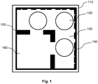
- Fig. 1 shows a semiconductor ship 110 comprising three mesas 120. Each of the mesas comprises an optical resonator. A principal sketch of such an optical resonator is shown in Fig. 2 .
- a metallization layer 130 is structured such that a bonding area 160 for electrically contacting the semiconductor chip 110 of the layer device is provided. Furthermore, alignment marks are provided in the metallization layer 130 for aligning the semiconductor chips 110 in the bonding process.
- the metallization layer 130 further comprises at the upper edge and the right edge a binary code 140 which comprises a number of extensions of different width. The extensions provide a binary code like a bar-code uniquely identifying each semiconductor chip 110. The binary code can be read out by means of optical inspection of the semiconductor chips 110.
- Fig. 2 shows a cross section of a VCSEL showing the optical resonator which is embedded in one of the mesas 120.
- the optical resonator comprises a bottom DBR 230 and a top DBR 240 and an active layer 260 sandwiched in between the bottom DBR 230 and the top DBR 240.
- the bottom DBR 230 is highly reflective (>99%) and the top DBR 240 does have a somewhat smaller reflectivity (>95%) in order to enable laser emission via the top DBR 240.
- the VCSEL is thus a so called top emitter.
- the active layer 260 comprises a number of layers building the Quantum Well structure.
- the bottom DBR 230 is arranged on a substrate like a GaAs-Substrate.
- the VCSEL is contacted by means of a bottom electrode 210 and a ring electrode 220.
- the bottom electrode 210 is provided on the side of the substrate opposite to the bottom DBR 230.
- the ring electrode 220 is provided on top of the top DBR 240.
- a confinement layer 250 is used to restrict the current flow through active area to a defined in this case circular area of the active layer.
- the confinement layer 250 comprises an electrically essentially nonconductive oxide area with a circular hole processed by lateral oxidization of the confinement layer 250 after etching the mesa.
- the confinement layer 250 is in this case arranged on top of the active layer 260.
- the confinement layer may also be positioned within the bottom DBR 230 or the top DBR 240. Variations of the arrangement of the layers without affecting the functionality of the layers are well known to those skilled in the art.
- Fig. 3 shows a principal sketch of a wafer 310 used to manufacture the semiconductor chips 110 of the laser device.
- the semiconductor chips 110 are delivered in sawn condition on UV tape.
- electronic-mapping is used instead of marking e.g. the bad dies or semiconductor chips 110 by means of inking.
- Reference dies 320 are positioned across the wafer such that good and bad semiconductor chips 110 can be detected by means of the electronic map aligned to the reference dies 320.
- the wafer further comprises test structures 330 which are provided in order to monitor the oxidation of the devices.
- the test structures 330 are, for example, VCSEL-like devices on some positions on the wafer that should just be completely oxidized or just be not completely oxidized.
- full contact mesas with outer diameter ranging from 18 ⁇ m to 22 ⁇ m in steps of 0.1um may be used as test structures 330.
- a mesa with a diameter of 20 ⁇ m should just be completely oxidized at a target oxidation width of 10 ⁇ m such that no electrical current is flows though the active layer.
- target oxidation width for example 9.5 ⁇ m actual oxidation width
- the confinement layer of the mesa shown in Fig. 2 would be completely oxidized in this case.
- the test structures 330 are integrated in the process such the test mesas are processed with normal bondpads and measured at the same time when 100% of the VCSELs or semiconductor chips are tested on the wafer prober. As each devices on the waferprober is measured much faster than a second, it is only very little additional time needed to measure the test structures 330 at this time in the process in order to control the lateral oxidation of the confinement layer of the mesas.
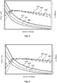
- Fig. 4 shows simulated performance data at 25°C depending on the number of mesas provided on the semiconductor chip 110.
- the applied electrical current is 12 mA.
- Line 410 shows the simulated voltage of laser devices depending on the number of mesas provided on the semiconductor chip 110.
- the production spread of the mesas is nominal - 1 Sigma meaning the active diameter of the mesas is smaller than the nominal active diameter.
- Line 420 shows the simulated voltage at the nominal value of the active diameter and line 430 the simulated voltage at the production spread of nominal + 1 Sigma.
- Lines 440, 450 and 460 show the respective simulated optical power emitted by the laser devices at a production spread of nominal - 1 Sigma, nominal and nominal + 1 Sigma depending on the number of mesas provided on the semiconductor chip 110 at 25°C.
- the spread of the emitted optical power is acceptable when between 2 and 6 mesas are provided on the semiconductor chip 110.
- One mesa causes a broad spread and the applied voltage is too high.
- the power spread is minimal if three mesas are provided and gets again unacceptable if more than six mesas are provided.
- the voltage decreases such that the voltage requirements are not fulfilled.
- Fig. 5 shows simulated performance data at 60°C depending on the number of mesas provided on the semiconductor chip 110.
- the applied electrical current is 12 mA.
- Line 510 shows the simulated voltage of laser devices depending on the number of mesas provided on the semiconductor chip 110.
- the production spread of the mesas is nominal - 1 Sigma.
- Line 520 shows the simulated voltage at the nominal value of the active diameter and line 530 the simulated voltage at the production spread of nominal + 1 Sigma.
- Lines 540, 550 and 560 show the respective simulated optical power at a production spread of nominal - 1 Sigma, nominal and nominal + 1 Sigma depending on the number of mesas provided on the semiconductor chip 110 at 60°C.
- the spread of the emitted optical power is acceptable when between 2 and 6 mesas are provided on the semiconductor chip.
- One mesa causes a broad spread and the applied voltage is too high.
- the power spread is minimal if three mesas are provided and gets unacceptable if more than six mesas are provided.
- the voltage decreases such that the voltage requirements are not fulfilled.
- Laser devices with semiconductor chips 110 with 2 to 6 mesas provided on the semiconductor chip 110 within the production spread of nominal +/- 1 Sigma thus fulfill the quality requirements within a temperature range of 25°C to 60°C and also in the temperature range between -10°C to 60°C.
- the latter temperature range is the temperature range of most applications and the spread empirically decreases at lower temperatures at least at moderate temperatures like -10°C.
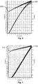
- Figs. 6 and 8 show the optical power and the electrical voltage of measured laser devices with a semiconductor chip comprising one mesa at 25°C and 60°C respectively.
- the applied electrical current was varied between 0 mA and 12 mA.
- the optical power versus current line 620 of several laser devices measured at 25°C is depicted in Fig. 6 .
- the emitted optical power depends essentially linearly from the applied electrical current in a range between 2 mA and around 7 mA. Additionally, the spread of the emitted optical power of the individual devices increases above an applied electrical current of around 8 mA. This behavior is even more pronounced at a substrate temperature of 60°C.
- the emitted optical power depends linearly on the applied electrical current only in a current range between 1 mA and around 6 mA as depicted by line 820.
- the spread of the emitted optical power increases and is much broader in comparison to the spread of 25°C.
- most of the measured laser devices emit less than 4 mW at 60°C
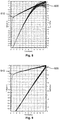
- Figs. 7 and 9 show the optical power and the electrical voltage of measured laser devices with a semiconductor chip comprising three mesas at 25°C and 60°C respectively.
- the applied electrical current was again varied between 0 mA and 12 mA.
- the optical power versus current line 720 of several laser devices measured at 25°C is depicted in Fig. 7 .
- the emitted optical power depends essentially linearly from the applied electrical current in a range between 2 mA and 12 mA. Additionally, the spread of the emitted optical power of the individual devices is low across the whole current range and doesn't increases above a threshold current. Furthermore, the behavior of the laser devices with three mesas is essentially the same at a substrate temperature of 60°C.
- the emitted optical power depends linearly on the applied electrical current in a current range between 2 mA and 12 mA. Only a minimum spread of the emitted optical power can be observed above 10 mA applied electrical current.
- the measured data shown in Figs. 6 - 9 thus impressively confirm the simulation data shown in Figs. 4 and 5 .
- the spread of emitted optical power at an applied electrical current of 12 mA is much lower for laser device comprising a semiconductor chip 110 with 3 mesas and reduced active diameter in comparison to a conventional semiconductor chip 110 with 1 mesa and increased active diameter.
- Most of the measured laser devices with one mesa even miss the specification of emitting at least 4 mW optical power at 12 mA and a substrate temperature of 60°C.
Description
- The invention relates to a VCSEL device wherein the VCSEL device is especially suited for sensing applications. The invention further relates to a method of marking semiconductor chips in a unique way.
- Laser devices for optical sensors often comprise Vertically Cavity Surface Emitting Lasers (VCSEL). Next generation require an optical output power of at least 6 mW. State of the art VCSELs with such high output power are realized by increasing the diameter of the aperture or active diameter of the VCSELs (~14um). At the same time the total die size needs to be as small as possible and yield of the laser device has to be high in order to meet the cost targets.
-
WO 2011/018734 A1 vertical cavity surface emitting laser (VCSEL)with active carrier confinement. It is proposed to integrate a phototransistor layer structure into the layer stack of the VCSEL. -
US 2013/0266326 A1 discloses microlenses for multibeam arrays of optoelectronic devices for high frequency operation. -
DE 199 54 093 A1 discloses an arrangement for high-power lasers. -
US 2012/0051685 A1 discloses flip-chip assembly comprising an array of vertical cavity surface emitting lasers (VCSELs). -
JP S55 87452 A -
WO 2002/005397 A2 discloses a VCSEL and VCSEL array having integrated microlenses for use in a semiconductor laser pumped solid state laser system. -
US 2009/0296752 A1 discloses a mulitple emitter VCSEL. An extended cavity surface emitting laser is proposed that has a first laser die with a first cavity and a first gain element and a second laser die with a second cavity and a second gain element. The first and second gain elements are in series to provide optical gain and optical feedback in an extended optical cavity configuration. The first and second gain elements provide optical gain and optical feedback in a common extended cavity with the first and second gain elements operating serially as a common extended cavity optical mode. - It's thus an object of the present invention to provide an improved laser device enabling a combination of a small die or chip size and high yield.
- According to a first aspect a laser device comprising between two and six mesas provided on one semiconductor chip is proposed. The mesas are electrically connected in parallel such that the mesas are adapted to emit laser light if a defined threshold voltage is provided to the mesas. The laser device further comprises a driver for electrically driving the mesas, wherein the driver is adapted to provide the defined threshold voltage to the mesas. The semiconductor chip has a side length of less than 250µm. The laser device is adapted to emit laser light of an optical power between 4 mW and 10 mW. Each mesa comprises an active diameter between 5 µm and 9 µm
- A laser device comprising only one mesa with increased diameter of the aperture may have the advantage that the size of device is small. Size is an essential factor because the chip area determines the number of semiconductor chips per wafer which can be manufactured in one run and therefore the prize of the laser device. Tests have shown that the production yield meaning the number of laser chips per wafer meeting the quality targets of such laser devices with one mesa is unsatisfactory. The production spread is high because of the tight process window. Further investigations have shown that providing between two and six mesas with smaller aperture and thus smaller optical power output per mesa on one semiconductor chip increases the yield and enables a lower temperature sensibility of the laser devices. The mesas are electrically connected in parallel such that in operation all mesas are provided with electrical power at the same time. All mesas on one semiconductor chip thus emit laser light at the same time. The lower temperature sensibility may be caused or at least positively influenced by the heat distribution when operating the two to six mesas in parallel in comparison to the concentrated heat dissipation in case of only one mesa per laser device. The latter effect may be even improved by distributing the between two and six mesas in a way that an even heat distribution is enabled across the laser device. The distance between the mesas may be maximized in relation to the available area on the semiconductor ship. Process steps like dicing and the like may require a minimum distance between a mesa and the edges of the semiconductor chip thus limiting the available area. The form of the chip may thus influence positioning of the mesas. In most cases quadratic semiconductor chips may be preferred. Despite of the fact that semiconductor chips with one mesa are smaller and enable more semiconductor chips the improved yield overcompensates the bigger size of the laser devices caused by the increased number of mesas.
- Surprisingly, it doesn't help to provide more than six mesas because the yield decreases again. The investigations have further shown that three mesas per laser device result in the highest yield. The three mesas may be preferably arranged on the available area of the semiconductor chip such that the centers of the mesas build an equilateral triangle in order to maximize the distance between the mesas. This arrangement of the mesas may enable an even distribution of the heat generated in each mesa across the semiconductor chip.
- The semiconductor chip of the laser device has a side length of less than 250µm. The size of the semiconductor chip determines the number of chips per wafer and thus strongly influences the prize of the laser device. It's the intention to provide semiconductor chips which are as small as possible. At the same time the requested optical power which has to be emitted by the laser devices increases, which would be easier if the chip size would be larger. The side length of the semiconductor chips may be even smaller than 250 µm like 200 µm or even smaller than 150 µm further decreasing the processing window.
- The laser devices are adapted to emit laser light of an optical power between 4 mW and 10 mW if they are connected to a corresponding driver and power source. The power source may be a conventional AC-line, a battery or any other power source being able to power the laser device and the corresponding driver. The kind of power source may depend on the application. Batteries which are preferably rechargeable may be used in mobile applications like, for example, proximity detection in mobile devices like mobile phones, smartphones, laptops and the like.
- The laser device is preferably adapted to be driven at a voltage between 1.6 V and 2.2 V at an electrical current of 12 mA when emitting laser light of an optical power between 4 mW and 10 mW. The laser device may be adapted to emit laser light of an optical power between 4 mW and 10 mW at a temperature of 60°C of the semiconductor chip. The temperature of the devices may often reach 60°C in operation. It's thus essential that the optical power doesn't drop below 4 mW in order to fulfill quality requirements. The temperature of the semiconductor chip is the temperature of the substrate of the semiconductor chip and not the local temperature in the active layer of the laser which may be considerably higher.
- The laser device is preferably adapted to emit laser light of an optical power at a temperature of 25°C of the semiconductor chip deviating less than 20% from the laser power emitted at 60°C of the semiconductor chip when driven at an electrical current of 12 mA. The deviation is most preferably even less than 10%. Some applications require a high temperature stability of the optical output power at a predetermined electrical driving current. High temperature stability of the laser device may reduce the requirements regarding the driving circuit. No additional sensors and/or feedback loops may be required in order to provide the requested optical power across a broad temperature range.
- The laser device is preferably adapted to emit laser light with an optical power, wherein the optical power linearly depends on the provided electrical current when driven at an electrical current between 3 mA and 12 mA. The linear dependence of the optical power from the electrical driving current may simplify the control of the optical output power in applications requesting such power control.
- The mesas comprise an active diameter between 5 µm and 9 µm in order to provide an optical power between 4 mW and 10 mW. In case of 2 - 4 mesas an active diameter between 7 µm and 9 µm may be preferred, whereby most efficient device may comprise mesas with an active diameter of 8 µm. In case of 5 - 6 mesas an active diameter between 5 µm and 7 µm may be preferred. The active diameter of a mesa is determined by means of an oxidation of a confinement layer within the mesas during processing of the wafer comprising the semiconductor chips. The active diameter restricts the electrical current to a defined area of an active layer within each mesa provided between a bottom and a top Distributed Bragg Reflector (DBR) with respect to the substrate of the semiconductor chip.
- The semiconductor chip may preferably comprise a functional layer with a coding for identifying the laser device. In view of the small chip size of preferably 150 µm × 150 µm or less chip numbers provided by means of well-known printing technology like inkjet printing may not be possible. A functional layer may thus be provided comprising a coding enabling an identification of each chip. The coding may be a bar-code provided in the functional layer such that the chip can be optically identified. The functional layer has thus to be visible after processing the semiconductor chip or the laser device. The functional layer may preferably be one of the layers needed for operating the laser device. One of the metallization layers may, for example, be etched such that besides the structure needed to manufacture and finally drive the laser device (e.g. electrical contacts) a bar-code like structure may be visible at one or more edges of the metallization layer. Such a binary code may be used to enable tracing of each laser device. The metallization layer used for tracing the laser device may, for example, additionally be used for bonding and contacting.
- Optical sensors for, for example, proximity detection may comprise one or more of the described laser devices. Using arrays comprising a multitude of mesas which can be individually addressed is known for power applications like printing and heating. These applications require high power laser devices providing an optical or laser power of several Watt or even several hundreds of Watt. The array of individually addressable mesas enables a simple switching of the emitted laser power. Optical sensors emit laser light with an optical power of only some mW such that more than one mesa per semiconductor chip seems to be undesirable. Anyhow, the improved yield and temperature stability of laser devices comprising between 2 and six mesas enable improved optical sensors like proximity sensors at reduced costs.
- Furthermore, an improved method of marking semiconductor chips especially small semiconductor chips for laser devices is described.
- The method comprises the steps of:
- providing a functional layer of the semiconductor chip; and
- structuring the functional layer in a way that a single semiconductor chip can be uniquely identified by means of optical detection.
- The method may enable an unambiguous marking of semiconductor chips or laser devices such that tracing of single, for example, laser devices is enabled. The tracing may be needed for quality management. Structuring of a functional layer like a metallization layer needed for, for example, electrically contacting avoids an additional manufacturing step like printing a serial number on top of the semiconductor chip. Marking of semiconductor chips may thus be simplified.
- It shall be understood that a preferred embodiment of the invention can also be any combination of the dependent claims with the respective independent claim.
- Further advantageous embodiments are defined below.
- These and other aspects of the invention will be apparent from and elucidated with reference to the embodiments described hereinafter.
- The invention will now be described, by way of example, based on embodiments with reference to the accompanying drawings.
- In the drawings:
-
Fig. 1 shows a a semiconductor ship comprising three mesas. -
Fig. 2 shows a cross section of a VCSEL showing the optical resonator embedded in a mesa. -
Fig. 3 shows a wafer used to manufacture semiconductor chips. -
Fig. 4 shows simulated performance data at 25°C depending on the number of mesas provided on the semiconductor chip. -
Fig. 5 shows simulated performance data at 60°C depending on the number of mesas provided on the semiconductor chip. -
Fig. 6 shows measured performance data at 25°C of a semiconductor chip with one mesa. -
Fig. 7 shows measured performance data at 25°C of a semiconductor chip with three mesas. -
Fig. 8 shows measured performance data at 60°C of a semiconductor chip with one mesa. -
Fig. 9 shows measured performance data at 60°C of a semiconductor chip with three mesas. - In the Figures, like numbers refer to like objects throughout. Objects in the Figures are not necessarily drawn to scale.
- Various embodiments of the invention will now be described by means of the Figures.
-
Fig. 1 shows asemiconductor ship 110 comprising threemesas 120. Each of the mesas comprises an optical resonator. A principal sketch of such an optical resonator is shown inFig. 2 . Ametallization layer 130 is structured such that abonding area 160 for electrically contacting thesemiconductor chip 110 of the layer device is provided. Furthermore, alignment marks are provided in themetallization layer 130 for aligning thesemiconductor chips 110 in the bonding process. Themetallization layer 130 further comprises at the upper edge and the right edge abinary code 140 which comprises a number of extensions of different width. The extensions provide a binary code like a bar-code uniquely identifying eachsemiconductor chip 110. The binary code can be read out by means of optical inspection of the semiconductor chips 110. -
Fig. 2 shows a cross section of a VCSEL showing the optical resonator which is embedded in one of themesas 120. The optical resonator comprises abottom DBR 230 and atop DBR 240 and anactive layer 260 sandwiched in between thebottom DBR 230 and thetop DBR 240. Thebottom DBR 230 is highly reflective (>99%) and thetop DBR 240 does have a somewhat smaller reflectivity (>95%) in order to enable laser emission via thetop DBR 240. The VCSEL is thus a so called top emitter. Theactive layer 260 comprises a number of layers building the Quantum Well structure. Thebottom DBR 230 is arranged on a substrate like a GaAs-Substrate. The VCSEL is contacted by means of abottom electrode 210 and aring electrode 220. Thebottom electrode 210 is provided on the side of the substrate opposite to thebottom DBR 230. Thering electrode 220 is provided on top of thetop DBR 240. Aconfinement layer 250 is used to restrict the current flow through active area to a defined in this case circular area of the active layer. Theconfinement layer 250 comprises an electrically essentially nonconductive oxide area with a circular hole processed by lateral oxidization of theconfinement layer 250 after etching the mesa. Theconfinement layer 250 is in this case arranged on top of theactive layer 260. The confinement layer may also be positioned within thebottom DBR 230 or thetop DBR 240. Variations of the arrangement of the layers without affecting the functionality of the layers are well known to those skilled in the art. -
Fig. 3 shows a principal sketch of awafer 310 used to manufacture thesemiconductor chips 110 of the laser device. The semiconductor chips 110 are delivered in sawn condition on UV tape. As the die size is of the semiconductor chips 110 is very small and inking cannot be used to show to the customer which semiconductor chip is good and which one is bad, electronic-mapping is used instead of marking e.g. the bad dies orsemiconductor chips 110 by means of inking. Reference dies 320 are positioned across the wafer such that good andbad semiconductor chips 110 can be detected by means of the electronic map aligned to the reference dies 320. The wafer further comprisestest structures 330 which are provided in order to monitor the oxidation of the devices. Thetest structures 330 are, for example, VCSEL-like devices on some positions on the wafer that should just be completely oxidized or just be not completely oxidized. For example, full contact mesas with outer diameter ranging from 18 µm to 22 µm in steps of 0.1um may be used astest structures 330. A mesa with a diameter of 20 µm should just be completely oxidized at a target oxidation width of 10 µm such that no electrical current is flows though the active layer. In case of some deviation from target oxidation width (for example 9.5 µm actual oxidation width), there is still some current flow in the mesa with 20 µm diameter, but no current in the 19 µm diameter mesa. The confinement layer of the mesa shown inFig. 2 would be completely oxidized in this case. Thetest structures 330 are integrated in the process such the test mesas are processed with normal bondpads and measured at the same time when 100% of the VCSELs or semiconductor chips are tested on the wafer prober. As each devices on the waferprober is measured much faster than a second, it is only very little additional time needed to measure thetest structures 330 at this time in the process in order to control the lateral oxidation of the confinement layer of the mesas. -
Fig. 4 shows simulated performance data at 25°C depending on the number of mesas provided on thesemiconductor chip 110. The applied electrical current is 12 mA.Line 410 shows the simulated voltage of laser devices depending on the number of mesas provided on thesemiconductor chip 110. The production spread of the mesas is nominal - 1 Sigma meaning the active diameter of the mesas is smaller than the nominal active diameter. Line 420 shows the simulated voltage at the nominal value of the active diameter andline 430 the simulated voltage at the production spread of nominal + 1 Sigma.Lines semiconductor chip 110 at 25°C. The spread of the emitted optical power is acceptable when between 2 and 6 mesas are provided on thesemiconductor chip 110. One mesa causes a broad spread and the applied voltage is too high. The power spread is minimal if three mesas are provided and gets again unacceptable if more than six mesas are provided. Furthermore, the voltage decreases such that the voltage requirements are not fulfilled. -
Fig. 5 shows simulated performance data at 60°C depending on the number of mesas provided on thesemiconductor chip 110. The applied electrical current is 12 mA.Line 510 shows the simulated voltage of laser devices depending on the number of mesas provided on thesemiconductor chip 110. The production spread of the mesas is nominal - 1 Sigma.Line 520 shows the simulated voltage at the nominal value of the active diameter andline 530 the simulated voltage at the production spread of nominal + 1 Sigma.Lines semiconductor chip 110 at 60°C. The spread of the emitted optical power is acceptable when between 2 and 6 mesas are provided on the semiconductor chip. One mesa causes a broad spread and the applied voltage is too high. The power spread is minimal if three mesas are provided and gets unacceptable if more than six mesas are provided. Furthermore, the voltage decreases such that the voltage requirements are not fulfilled. Laser devices withsemiconductor chips 110 with 2 to 6 mesas provided on thesemiconductor chip 110 within the production spread of nominal +/- 1 Sigma thus fulfill the quality requirements within a temperature range of 25°C to 60°C and also in the temperature range between -10°C to 60°C. The latter temperature range is the temperature range of most applications and the spread empirically decreases at lower temperatures at least at moderate temperatures like -10°C. -
Figs. 6 and8 show the optical power and the electrical voltage of measured laser devices with a semiconductor chip comprising one mesa at 25°C and 60°C respectively. The applied electrical current was varied between 0 mA and 12 mA. The optical power versus current line 620 of several laser devices measured at 25°C is depicted inFig. 6 . The emitted optical power depends essentially linearly from the applied electrical current in a range between 2 mA and around 7 mA. Additionally, the spread of the emitted optical power of the individual devices increases above an applied electrical current of around 8 mA. This behavior is even more pronounced at a substrate temperature of 60°C. The emitted optical power depends linearly on the applied electrical current only in a current range between 1 mA and around 6 mA as depicted byline 820. Already at 6 mA the spread of the emitted optical power increases and is much broader in comparison to the spread of 25°C. Furthermore, most of the measured laser devices emit less than 4 mW at 60°C -
Figs. 7 and9 show the optical power and the electrical voltage of measured laser devices with a semiconductor chip comprising three mesas at 25°C and 60°C respectively. The applied electrical current was again varied between 0 mA and 12 mA. The optical power versuscurrent line 720 of several laser devices measured at 25°C is depicted inFig. 7 . The emitted optical power depends essentially linearly from the applied electrical current in a range between 2 mA and 12 mA. Additionally, the spread of the emitted optical power of the individual devices is low across the whole current range and doesn't increases above a threshold current. Furthermore, the behavior of the laser devices with three mesas is essentially the same at a substrate temperature of 60°C. The emitted optical power depends linearly on the applied electrical current in a current range between 2 mA and 12 mA. Only a minimum spread of the emitted optical power can be observed above 10 mA applied electrical current. - The measured data shown in
Figs. 6 - 9 thus impressively confirm the simulation data shown inFigs. 4 and 5 . The spread of emitted optical power at an applied electrical current of 12 mA is much lower for laser device comprising asemiconductor chip 110 with 3 mesas and reduced active diameter in comparison to aconventional semiconductor chip 110 with 1 mesa and increased active diameter. Most of the measured laser devices with one mesa even miss the specification of emitting at least 4 mW optical power at 12 mA and a substrate temperature of 60°C. - While the invention has been illustrated and described in detail in the drawings and the foregoing description, such illustration and description are to be considered illustrative or exemplary and not restrictive.
- From reading the present disclosure, other modifications will be apparent to persons skilled in the art. Such modifications may involve other features which are already known in the art and which may be used instead of or in addition to features already described herein.
- Variations to the disclosed embodiments can be understood and effected by those skilled in the art, from a study of the drawings, the disclosure and the appended claims. In the claims, the word "comprising" does not exclude other elements or steps, and the indefinite article "a" or "an" does not exclude a plurality of elements or steps. The mere fact that certain measures are recited in mutually different dependent claims does not indicate that a combination of these measures cannot be used to advantage.
- Any reference signs in the claims should not be construed as limiting the scope thereof.
-
- 110
- semiconductor chip
- 120
- mesa
- 130
- metallization layer
- 140
- binary code
- 150
- alignment marks
- 160
- bonding area
- 210
- bottom electrode
- 220
- ring electrode
- 230
- bottom DBR
- 240
- top DBR
- 250
- confinement layer
- 260
- active layer
- 270
- substrate
- 310
- wafer
- 320
- reference die
- 330
- test structure
- 410
- voltage versus number of mesas nominal-sigma at 25°C
- 420
- voltage versus number of mesas nominal at 25°C
- 430
- voltage versus number of mesas nominal+sigma at 25°C
- 440
- power versus number of mesas nominal-sigma at 25°C
- 450
- power versus number of mesas nominal at 25°C
- 460
- power versus number of mesas nominal+sigma at 25°C
- 510
- voltage versus number of mesas nominal-sigma at 60°C
- 520
- voltage versus number of mesas nominal at 60°C
- 530
- voltage versus number of mesas nominal+sigma at 60°C
- 540
- power versus number of mesas nominal-sigma at 60°C
- 550
- power versus number of mesas nominal at 60°C
- 560
- power versus number of mesas nominal+sigma at 60°C
- 610
- voltage versus current one mesa at 25°C
- 620
- power versus current one mesa at 25°C
- 710
- voltage versus current three mesas at 25°C
- 720
- power versus current three mesas at 25°C
- 810
- voltage versus current one mesa at 60°C
- 820
- power versus current one mesa at 60°C
- 910
- voltage versus current three mesas at 60°C
- 920
- power versus current three mesas at 60°C
Claims (11)
- A VCSEL device comprising between three and six mesas (120) provided on one semiconductor chip (110), wherein the mesas (120) are electrically connected in parallel such that the mesas (120) are adapted to emit laser light at the same time if a defined voltage is provided to the mesas (120), the laser device further comprising a driver for electrically driving the mesas, wherein the driver is adapted to provide the defined voltage to the mesas (120); wherein the semiconductor chip (110) has a side length of less than 250µm; wherein the VCSEL device is adapted to emit laser light of an optical power between 4 mW and 10 mW; and wherein each mesa comprises an active diameter of a circular hole defined by a non-conductive oxide area between 5 µm and 9 µm.
- The VCSEL device according to claim 1 comprising three mesas (120).
- The VCSEL device according to claim 1 or 2, wherein the VCSEL device is adapted to be driven at a voltage between 1.6 V and 2.2 V at an electrical current of 12 mA when emitting laser light of an optical power between 4 mW and 10 mW.
- The VCSEL device according to claim 1 or 2, wherein the VCSEL device is adapted to emit laser light of an optical power between 4 mW and 10 mW at a temperature of 60°C of the semiconductor chip (110).
- The VCSEL device according to claim 4, wherein the VCSEL device is adapted to emit laser light of an optical power at a temperature of 25°C of the semiconductor chip (110) deviating less than 20% from the laser power emitted at 60°C of the semiconductor chip when driven at an electrical current of 12 mA.
- The VCSEL device according to claim 1 or 2, wherein the VCSEL device is adapted to emit laser light with an optical power, wherein the optical power linearly depends on the provided electrical current when driven at an electrical current between 3 mA and 12 mA.
- The VCSEL device according to claim 1 or 2, wherein the semiconductor chip (110) comprises a functional layer, the functional layer comprising a coding for identifying the VCSEL device.
- The VCSEL device according to claim 7, wherein the functional layer is a metallization layer of the semiconductor chip (110).
- The VCSEL device according to claim 8, wherein the metallization layer comprises a binary coding at at least one edge of the semiconductor chip (110).
- The VCSEL device according to claim 1 or 2, wherein the mesas are distributed on the semiconductor chip (110) in a way such that an even heat distribution is enabled across the semiconductor chip (110).
- An optical sensor comprising the VCSEL device according to any of the claims 1 to 10.
Priority Applications (1)
| Application Number | Priority Date | Filing Date | Title |
|---|---|---|---|
| EP14783863.5A EP3058592B1 (en) | 2013-10-16 | 2014-10-14 | Compact laser device |
Applications Claiming Priority (3)
| Application Number | Priority Date | Filing Date | Title |
|---|---|---|---|
| EP13188872 | 2013-10-16 | ||
| PCT/EP2014/071938 WO2015055600A1 (en) | 2013-10-16 | 2014-10-14 | Compact laser device |
| EP14783863.5A EP3058592B1 (en) | 2013-10-16 | 2014-10-14 | Compact laser device |
Publications (2)
| Publication Number | Publication Date |
|---|---|
| EP3058592A1 EP3058592A1 (en) | 2016-08-24 |
| EP3058592B1 true EP3058592B1 (en) | 2021-12-29 |
Family
ID=49356317
Family Applications (1)
| Application Number | Title | Priority Date | Filing Date |
|---|---|---|---|
| EP14783863.5A Active EP3058592B1 (en) | 2013-10-16 | 2014-10-14 | Compact laser device |
Country Status (6)
| Country | Link |
|---|---|
| US (2) | US10116119B2 (en) |
| EP (1) | EP3058592B1 (en) |
| JP (1) | JP6550381B2 (en) |
| CN (1) | CN105637634A (en) |
| RU (1) | RU2672155C2 (en) |
| WO (1) | WO2015055600A1 (en) |
Families Citing this family (5)
| Publication number | Priority date | Publication date | Assignee | Title |
|---|---|---|---|---|
| CN105637634A (en) * | 2013-10-16 | 2016-06-01 | 皇家飞利浦有限公司 | Compact laser device |
| RU2712939C2 (en) * | 2015-04-10 | 2020-02-03 | Конинклейке Филипс Н.В. | Safe laser device for optical probing applications |
| EP3217428B1 (en) * | 2016-03-07 | 2022-09-07 | Infineon Technologies AG | Multiple substrate and method for the production of same |
| JP2017204640A (en) | 2016-05-11 | 2017-11-16 | 晶元光電股▲ふん▼有限公司Epistar Corporation | Light-emitting device and method for manufacturing the same |
| EP3392290B8 (en) * | 2017-04-18 | 2020-11-11 | Ems-Chemie Ag | Polyamide moulding material and molded bodies made from same |
Citations (2)
| Publication number | Priority date | Publication date | Assignee | Title |
|---|---|---|---|---|
| WO2002005397A2 (en) * | 2000-07-12 | 2002-01-17 | Princeton Optronics, Inc. | Vcsel and vcsel array having integrated microlenses for use in a semiconductor laser pumped solid state laser system |
| US20090296752A1 (en) * | 2007-06-14 | 2009-12-03 | Giorgio Giaretta | Multiple emitter vecsel |
Family Cites Families (28)
| Publication number | Priority date | Publication date | Assignee | Title |
|---|---|---|---|---|
| JPS5587452A (en) * | 1978-12-26 | 1980-07-02 | Fujitsu Ltd | Manufacture of semiconductor device |
| US6272160B1 (en) * | 1998-02-03 | 2001-08-07 | Applied Micro Circuits Corporation | High-speed CMOS driver for vertical-cavity surface-emitting lasers |
| US6465744B2 (en) * | 1998-03-27 | 2002-10-15 | Tessera, Inc. | Graded metallic leads for connection to microelectronic elements |
| DE19954093A1 (en) * | 1999-11-10 | 2001-05-23 | Infineon Technologies Ag | Arrangement for high power lasers |
| US6465774B1 (en) * | 2000-06-30 | 2002-10-15 | Honeywell International Inc. | Method and system for versatile optical sensor package |
| US6415977B1 (en) * | 2000-08-30 | 2002-07-09 | Micron Technology, Inc. | Method and apparatus for marking and identifying a defective die site |
| US7085300B2 (en) * | 2001-12-28 | 2006-08-01 | Finisar Corporation | Integral vertical cavity surface emitting laser and power monitor |
| US7164702B1 (en) * | 2003-08-29 | 2007-01-16 | The United States Of America As Represented By The Secretary Of The Army | Optical transmitters and interconnects using surface-emitting lasers and micro-optical elements |
| JP2005158945A (en) * | 2003-11-25 | 2005-06-16 | Fanuc Ltd | Semiconductor laser device |
| JP4584066B2 (en) * | 2004-12-10 | 2010-11-17 | 韓國電子通信研究院 | Surface emitting laser device having photosensor and optical waveguide device using the same |
| JP4839662B2 (en) * | 2005-04-08 | 2011-12-21 | 富士ゼロックス株式会社 | Surface emitting semiconductor laser array and optical transmission system using the same |
| JP5055717B2 (en) | 2005-06-20 | 2012-10-24 | 富士ゼロックス株式会社 | Surface emitting semiconductor laser |
| US7233025B2 (en) * | 2005-11-10 | 2007-06-19 | Microsoft Corporation | Electronic packaging for optical emitters and sensors |
| JP5034662B2 (en) | 2006-06-20 | 2012-09-26 | ソニー株式会社 | Surface emitting semiconductor laser and manufacturing method thereof |
| KR100990702B1 (en) * | 2006-08-23 | 2010-10-29 | 가부시키가이샤 리코 | Surface-emitting laser array, optical scanning device, and image forming device |
| JP4858032B2 (en) * | 2006-09-15 | 2012-01-18 | 日亜化学工業株式会社 | Light emitting device |
| KR101360294B1 (en) * | 2008-05-21 | 2014-02-11 | 광주과학기술원 | A reflection type optics sensor device |
| JP5261754B2 (en) * | 2008-11-27 | 2013-08-14 | 株式会社リコー | Surface emitting laser element, surface emitting laser array, optical scanning device, and image forming apparatus |
| US7949024B2 (en) | 2009-02-17 | 2011-05-24 | Trilumina Corporation | Multibeam arrays of optoelectronic devices for high frequency operation |
| US8995493B2 (en) * | 2009-02-17 | 2015-03-31 | Trilumina Corp. | Microlenses for multibeam arrays of optoelectronic devices for high frequency operation |
| KR101698556B1 (en) | 2009-02-25 | 2017-02-01 | 코닌클리케 필립스 엔.브이. | Output power stabilization for laser diodes using the photon-cooling dependent laser voltage |
| JP6026884B2 (en) * | 2009-08-10 | 2016-11-16 | コーニンクレッカ フィリップス エヌ ヴェKoninklijke Philips N.V. | Vertical cavity surface emitting laser with active carrier confinement. |
| US9620934B2 (en) * | 2010-08-31 | 2017-04-11 | Avago Technologies General Ip (Singapore) Pte. Ltd. | Flip-chip assembly comprising an array of vertical cavity surface emitting lasers (VCSELs) |
| JP5874227B2 (en) | 2011-07-22 | 2016-03-02 | 富士ゼロックス株式会社 | Surface emitting semiconductor laser array, surface emitting semiconductor laser device, optical transmission device, and information processing device |
| US9088134B2 (en) * | 2011-07-27 | 2015-07-21 | Vixar Inc. | Method and apparatus including improved vertical-cavity surface-emitting lasers |
| CN104170188A (en) | 2012-03-14 | 2014-11-26 | 皇家飞利浦有限公司 | VCSEL module and manufacture thereof |
| JP5477728B2 (en) * | 2013-05-13 | 2014-04-23 | 株式会社リコー | Surface emitting laser array |
| CN105637634A (en) * | 2013-10-16 | 2016-06-01 | 皇家飞利浦有限公司 | Compact laser device |
-
2014
- 2014-10-14 CN CN201480056961.2A patent/CN105637634A/en active Pending
- 2014-10-14 WO PCT/EP2014/071938 patent/WO2015055600A1/en active Application Filing
- 2014-10-14 US US15/028,546 patent/US10116119B2/en active Active
- 2014-10-14 RU RU2016118623A patent/RU2672155C2/en not_active IP Right Cessation
- 2014-10-14 JP JP2016522763A patent/JP6550381B2/en active Active
- 2014-10-14 EP EP14783863.5A patent/EP3058592B1/en active Active
-
2018
- 2018-10-18 US US16/164,209 patent/US10707646B2/en active Active
Patent Citations (2)
| Publication number | Priority date | Publication date | Assignee | Title |
|---|---|---|---|---|
| WO2002005397A2 (en) * | 2000-07-12 | 2002-01-17 | Princeton Optronics, Inc. | Vcsel and vcsel array having integrated microlenses for use in a semiconductor laser pumped solid state laser system |
| US20090296752A1 (en) * | 2007-06-14 | 2009-12-03 | Giorgio Giaretta | Multiple emitter vecsel |
Also Published As
| Publication number | Publication date |
|---|---|
| RU2016118623A3 (en) | 2018-05-15 |
| WO2015055600A1 (en) | 2015-04-23 |
| US10116119B2 (en) | 2018-10-30 |
| US20160254640A1 (en) | 2016-09-01 |
| US20190052048A1 (en) | 2019-02-14 |
| EP3058592A1 (en) | 2016-08-24 |
| JP2016533639A (en) | 2016-10-27 |
| CN105637634A (en) | 2016-06-01 |
| RU2672155C2 (en) | 2018-11-12 |
| RU2016118623A (en) | 2017-11-20 |
| US10707646B2 (en) | 2020-07-07 |
| JP6550381B2 (en) | 2019-07-24 |
Similar Documents
| Publication | Publication Date | Title |
|---|---|---|
| US10707646B2 (en) | Compact laser device | |
| CN116325394A (en) | 3D and LiDAR sensing modules | |
| US10962627B2 (en) | Ultra-small vertical cavity surface emitting laser (VCSEL) and arrays incorporating the same | |
| US11271365B2 (en) | Laser element | |
| US20070091962A1 (en) | Substrate for vertical cavity surface emitting laser ( VCSEL) and method for manufacturing VCSEL device | |
| US8624614B2 (en) | Burn-in method for surface emitting semiconductor laser device | |
| CN112335143A (en) | VCSEL array with small pulse delay | |
| CN112970156A (en) | Small pitch VCSEL array | |
| US20200194966A1 (en) | Light source package | |
| JP4821967B2 (en) | Semiconductor laser device and optical transmitter using the same | |
| US20210320479A1 (en) | Light-emitting element array chip, light-emitting device, optical device, and information processing device | |
| US20110003403A1 (en) | Testing method of surface-emitting laser device and testing device thereof | |
| JP4501404B2 (en) | Method for evaluating semiconductor light emitting device | |
| US11588301B2 (en) | Vertical cavity surface emitting laser device | |
| EP4092848A1 (en) | Densely packed vcsel array | |
| EP3742563A1 (en) | Vertical cavity surface emitting laser device, laser light source and method of operating a laser light source | |
| Song et al. | 3D integrated 2D addressable VCSEL array with highly uniform short pulse characteristics | |
| JP2023042124A (en) | Light-emitting device and light-measuring apparatus | |
| CN113594853A (en) | Multi-layer metallization of multi-channel transmitter arrays | |
| CN117595062A (en) | Vertical cavity surface emitting laser array structure | |
| CN115693390A (en) | Vertical cavity surface emitting laser and electronic equipment with same | |
| Roose et al. | Final report on LDRD project: advanced optical trigger systems. |
Legal Events
| Date | Code | Title | Description |
|---|---|---|---|
| PUAI | Public reference made under article 153(3) epc to a published international application that has entered the european phase |
Free format text: ORIGINAL CODE: 0009012 |
|
| 17P | Request for examination filed |
Effective date: 20160517 |
|
| AK | Designated contracting states |
Kind code of ref document: A1 Designated state(s): AL AT BE BG CH CY CZ DE DK EE ES FI FR GB GR HR HU IE IS IT LI LT LU LV MC MK MT NL NO PL PT RO RS SE SI SK SM TR |
|
| AX | Request for extension of the european patent |
Extension state: BA ME |
|
| DAX | Request for extension of the european patent (deleted) | ||
| STAA | Information on the status of an ep patent application or granted ep patent |
Free format text: STATUS: EXAMINATION IS IN PROGRESS |
|
| 17Q | First examination report despatched |
Effective date: 20190614 |
|
| STAA | Information on the status of an ep patent application or granted ep patent |
Free format text: STATUS: EXAMINATION IS IN PROGRESS |
|
| RAP1 | Party data changed (applicant data changed or rights of an application transferred) |
Owner name: KONINKLIJKE PHILIPS N.V. |
|
| RAP1 | Party data changed (applicant data changed or rights of an application transferred) |
Owner name: TRUMPF PHOTONIC COMPONENTS GMBH |
|
| GRAP | Despatch of communication of intention to grant a patent |
Free format text: ORIGINAL CODE: EPIDOSNIGR1 |
|
| STAA | Information on the status of an ep patent application or granted ep patent |
Free format text: STATUS: GRANT OF PATENT IS INTENDED |
|
| INTG | Intention to grant announced |
Effective date: 20210726 |
|
| GRAS | Grant fee paid |
Free format text: ORIGINAL CODE: EPIDOSNIGR3 |
|
| GRAA | (expected) grant |
Free format text: ORIGINAL CODE: 0009210 |
|
| STAA | Information on the status of an ep patent application or granted ep patent |
Free format text: STATUS: THE PATENT HAS BEEN GRANTED |
|
| AK | Designated contracting states |
Kind code of ref document: B1 Designated state(s): AL AT BE BG CH CY CZ DE DK EE ES FI FR GB GR HR HU IE IS IT LI LT LU LV MC MK MT NL NO PL PT RO RS SE SI SK SM TR |
|
| REG | Reference to a national code |
Ref country code: GB Ref legal event code: FG4D |
|
| REG | Reference to a national code |
Ref country code: CH Ref legal event code: EP |
|
| REG | Reference to a national code |
Ref country code: AT Ref legal event code: REF Ref document number: 1459327 Country of ref document: AT Kind code of ref document: T Effective date: 20220115 |
|
| REG | Reference to a national code |
Ref country code: IE Ref legal event code: FG4D |
|
| REG | Reference to a national code |
Ref country code: DE Ref legal event code: R096 Ref document number: 602014081919 Country of ref document: DE |
|
| REG | Reference to a national code |
Ref country code: LT Ref legal event code: MG9D |
|
| PG25 | Lapsed in a contracting state [announced via postgrant information from national office to epo] |
Ref country code: RS Free format text: LAPSE BECAUSE OF FAILURE TO SUBMIT A TRANSLATION OF THE DESCRIPTION OR TO PAY THE FEE WITHIN THE PRESCRIBED TIME-LIMIT Effective date: 20211229 Ref country code: LT Free format text: LAPSE BECAUSE OF FAILURE TO SUBMIT A TRANSLATION OF THE DESCRIPTION OR TO PAY THE FEE WITHIN THE PRESCRIBED TIME-LIMIT Effective date: 20211229 Ref country code: FI Free format text: LAPSE BECAUSE OF FAILURE TO SUBMIT A TRANSLATION OF THE DESCRIPTION OR TO PAY THE FEE WITHIN THE PRESCRIBED TIME-LIMIT Effective date: 20211229 Ref country code: BG Free format text: LAPSE BECAUSE OF FAILURE TO SUBMIT A TRANSLATION OF THE DESCRIPTION OR TO PAY THE FEE WITHIN THE PRESCRIBED TIME-LIMIT Effective date: 20220329 |
|
| REG | Reference to a national code |
Ref country code: NL Ref legal event code: MP Effective date: 20211229 |
|
| PG25 | Lapsed in a contracting state [announced via postgrant information from national office to epo] |
Ref country code: SE Free format text: LAPSE BECAUSE OF FAILURE TO SUBMIT A TRANSLATION OF THE DESCRIPTION OR TO PAY THE FEE WITHIN THE PRESCRIBED TIME-LIMIT Effective date: 20211229 Ref country code: NO Free format text: LAPSE BECAUSE OF FAILURE TO SUBMIT A TRANSLATION OF THE DESCRIPTION OR TO PAY THE FEE WITHIN THE PRESCRIBED TIME-LIMIT Effective date: 20220329 Ref country code: LV Free format text: LAPSE BECAUSE OF FAILURE TO SUBMIT A TRANSLATION OF THE DESCRIPTION OR TO PAY THE FEE WITHIN THE PRESCRIBED TIME-LIMIT Effective date: 20211229 Ref country code: HR Free format text: LAPSE BECAUSE OF FAILURE TO SUBMIT A TRANSLATION OF THE DESCRIPTION OR TO PAY THE FEE WITHIN THE PRESCRIBED TIME-LIMIT Effective date: 20211229 Ref country code: GR Free format text: LAPSE BECAUSE OF FAILURE TO SUBMIT A TRANSLATION OF THE DESCRIPTION OR TO PAY THE FEE WITHIN THE PRESCRIBED TIME-LIMIT Effective date: 20220330 |
|
| PG25 | Lapsed in a contracting state [announced via postgrant information from national office to epo] |
Ref country code: NL Free format text: LAPSE BECAUSE OF FAILURE TO SUBMIT A TRANSLATION OF THE DESCRIPTION OR TO PAY THE FEE WITHIN THE PRESCRIBED TIME-LIMIT Effective date: 20211229 |
|
| PG25 | Lapsed in a contracting state [announced via postgrant information from national office to epo] |
Ref country code: SM Free format text: LAPSE BECAUSE OF FAILURE TO SUBMIT A TRANSLATION OF THE DESCRIPTION OR TO PAY THE FEE WITHIN THE PRESCRIBED TIME-LIMIT Effective date: 20211229 Ref country code: SK Free format text: LAPSE BECAUSE OF FAILURE TO SUBMIT A TRANSLATION OF THE DESCRIPTION OR TO PAY THE FEE WITHIN THE PRESCRIBED TIME-LIMIT Effective date: 20211229 Ref country code: RO Free format text: LAPSE BECAUSE OF FAILURE TO SUBMIT A TRANSLATION OF THE DESCRIPTION OR TO PAY THE FEE WITHIN THE PRESCRIBED TIME-LIMIT Effective date: 20211229 Ref country code: PT Free format text: LAPSE BECAUSE OF FAILURE TO SUBMIT A TRANSLATION OF THE DESCRIPTION OR TO PAY THE FEE WITHIN THE PRESCRIBED TIME-LIMIT Effective date: 20220429 Ref country code: ES Free format text: LAPSE BECAUSE OF FAILURE TO SUBMIT A TRANSLATION OF THE DESCRIPTION OR TO PAY THE FEE WITHIN THE PRESCRIBED TIME-LIMIT Effective date: 20211229 Ref country code: EE Free format text: LAPSE BECAUSE OF FAILURE TO SUBMIT A TRANSLATION OF THE DESCRIPTION OR TO PAY THE FEE WITHIN THE PRESCRIBED TIME-LIMIT Effective date: 20211229 Ref country code: CZ Free format text: LAPSE BECAUSE OF FAILURE TO SUBMIT A TRANSLATION OF THE DESCRIPTION OR TO PAY THE FEE WITHIN THE PRESCRIBED TIME-LIMIT Effective date: 20211229 |
|
| PG25 | Lapsed in a contracting state [announced via postgrant information from national office to epo] |
Ref country code: PL Free format text: LAPSE BECAUSE OF FAILURE TO SUBMIT A TRANSLATION OF THE DESCRIPTION OR TO PAY THE FEE WITHIN THE PRESCRIBED TIME-LIMIT Effective date: 20211229 |
|
| PG25 | Lapsed in a contracting state [announced via postgrant information from national office to epo] |
Ref country code: IS Free format text: LAPSE BECAUSE OF FAILURE TO SUBMIT A TRANSLATION OF THE DESCRIPTION OR TO PAY THE FEE WITHIN THE PRESCRIBED TIME-LIMIT Effective date: 20220429 |
|
| REG | Reference to a national code |
Ref country code: DE Ref legal event code: R097 Ref document number: 602014081919 Country of ref document: DE |
|
| PG25 | Lapsed in a contracting state [announced via postgrant information from national office to epo] |
Ref country code: DK Free format text: LAPSE BECAUSE OF FAILURE TO SUBMIT A TRANSLATION OF THE DESCRIPTION OR TO PAY THE FEE WITHIN THE PRESCRIBED TIME-LIMIT Effective date: 20211229 Ref country code: AL Free format text: LAPSE BECAUSE OF FAILURE TO SUBMIT A TRANSLATION OF THE DESCRIPTION OR TO PAY THE FEE WITHIN THE PRESCRIBED TIME-LIMIT Effective date: 20211229 |
|
| PLBE | No opposition filed within time limit |
Free format text: ORIGINAL CODE: 0009261 |
|
| STAA | Information on the status of an ep patent application or granted ep patent |
Free format text: STATUS: NO OPPOSITION FILED WITHIN TIME LIMIT |
|
| 26N | No opposition filed |
Effective date: 20220930 |
|
| PG25 | Lapsed in a contracting state [announced via postgrant information from national office to epo] |
Ref country code: SI Free format text: LAPSE BECAUSE OF FAILURE TO SUBMIT A TRANSLATION OF THE DESCRIPTION OR TO PAY THE FEE WITHIN THE PRESCRIBED TIME-LIMIT Effective date: 20211229 |
|
| REG | Reference to a national code |
Ref country code: AT Ref legal event code: UEP Ref document number: 1459327 Country of ref document: AT Kind code of ref document: T Effective date: 20211229 |
|
| PG25 | Lapsed in a contracting state [announced via postgrant information from national office to epo] |
Ref country code: MC Free format text: LAPSE BECAUSE OF FAILURE TO SUBMIT A TRANSLATION OF THE DESCRIPTION OR TO PAY THE FEE WITHIN THE PRESCRIBED TIME-LIMIT Effective date: 20211229 Ref country code: IT Free format text: LAPSE BECAUSE OF FAILURE TO SUBMIT A TRANSLATION OF THE DESCRIPTION OR TO PAY THE FEE WITHIN THE PRESCRIBED TIME-LIMIT Effective date: 20211229 |
|
| REG | Reference to a national code |
Ref country code: CH Ref legal event code: PL |
|
| REG | Reference to a national code |
Ref country code: BE Ref legal event code: MM Effective date: 20221031 |
|
| PG25 | Lapsed in a contracting state [announced via postgrant information from national office to epo] |
Ref country code: LU Free format text: LAPSE BECAUSE OF NON-PAYMENT OF DUE FEES Effective date: 20221014 |
|
| PG25 | Lapsed in a contracting state [announced via postgrant information from national office to epo] |
Ref country code: LI Free format text: LAPSE BECAUSE OF NON-PAYMENT OF DUE FEES Effective date: 20221031 Ref country code: CH Free format text: LAPSE BECAUSE OF NON-PAYMENT OF DUE FEES Effective date: 20221031 |
|
| PG25 | Lapsed in a contracting state [announced via postgrant information from national office to epo] |
Ref country code: BE Free format text: LAPSE BECAUSE OF NON-PAYMENT OF DUE FEES Effective date: 20221031 |
|
| PG25 | Lapsed in a contracting state [announced via postgrant information from national office to epo] |
Ref country code: IE Free format text: LAPSE BECAUSE OF NON-PAYMENT OF DUE FEES Effective date: 20221014 |
|
| PGFP | Annual fee paid to national office [announced via postgrant information from national office to epo] |
Ref country code: GB Payment date: 20231020 Year of fee payment: 10 |
|
| PGFP | Annual fee paid to national office [announced via postgrant information from national office to epo] |
Ref country code: FR Payment date: 20231026 Year of fee payment: 10 Ref country code: DE Payment date: 20231020 Year of fee payment: 10 Ref country code: AT Payment date: 20231020 Year of fee payment: 10 |
|
| PG25 | Lapsed in a contracting state [announced via postgrant information from national office to epo] |
Ref country code: HU Free format text: LAPSE BECAUSE OF FAILURE TO SUBMIT A TRANSLATION OF THE DESCRIPTION OR TO PAY THE FEE WITHIN THE PRESCRIBED TIME-LIMIT; INVALID AB INITIO Effective date: 20141014 |