EP3055918B1 - System for capacitively driving a load - Google Patents
System for capacitively driving a load Download PDFInfo
- Publication number
- EP3055918B1 EP3055918B1 EP14781566.6A EP14781566A EP3055918B1 EP 3055918 B1 EP3055918 B1 EP 3055918B1 EP 14781566 A EP14781566 A EP 14781566A EP 3055918 B1 EP3055918 B1 EP 3055918B1
- Authority
- EP
- European Patent Office
- Prior art keywords
- capacitive
- load
- series
- capacitance
- electrodes
- Prior art date
- Legal status (The legal status is an assumption and is not a legal conclusion. Google has not performed a legal analysis and makes no representation as to the accuracy of the status listed.)
- Not-in-force
Links
Images


Classifications
-
- H—ELECTRICITY
- H05—ELECTRIC TECHNIQUES NOT OTHERWISE PROVIDED FOR
- H05B—ELECTRIC HEATING; ELECTRIC LIGHT SOURCES NOT OTHERWISE PROVIDED FOR; CIRCUIT ARRANGEMENTS FOR ELECTRIC LIGHT SOURCES, IN GENERAL
- H05B45/00—Circuit arrangements for operating light-emitting diodes [LED]
-
- H—ELECTRICITY
- H02—GENERATION; CONVERSION OR DISTRIBUTION OF ELECTRIC POWER
- H02J—CIRCUIT ARRANGEMENTS OR SYSTEMS FOR SUPPLYING OR DISTRIBUTING ELECTRIC POWER; SYSTEMS FOR STORING ELECTRIC ENERGY
- H02J50/00—Circuit arrangements or systems for wireless supply or distribution of electric power
- H02J50/05—Circuit arrangements or systems for wireless supply or distribution of electric power using capacitive coupling
-
- H—ELECTRICITY
- H05—ELECTRIC TECHNIQUES NOT OTHERWISE PROVIDED FOR
- H05B—ELECTRIC HEATING; ELECTRIC LIGHT SOURCES NOT OTHERWISE PROVIDED FOR; CIRCUIT ARRANGEMENTS FOR ELECTRIC LIGHT SOURCES, IN GENERAL
- H05B45/00—Circuit arrangements for operating light-emitting diodes [LED]
- H05B45/40—Details of LED load circuits
- H05B45/44—Details of LED load circuits with an active control inside an LED matrix
- H05B45/48—Details of LED load circuits with an active control inside an LED matrix having LEDs organised in strings and incorporating parallel shunting devices
Definitions
- the present invention relates in general to the field of wireless power transfer to a load device.
- the load device is a lighting device including one or more light-generating units.
- the transfer involves the charging of a battery of an appliance, for instance a telephone. The invention will be specifically explained for these examples without intending to limit the scope of the invention to these examples.
- the housing of the load device may contain a receiver coil, which for power transfer will be coupled to a transmission coil in a docking station, the two coupled coils basically constitute a transformer.
- the load device will include at least one receiver electrode which for power transfer will be coupled capacitively to a transmission electrode in a supply structure such as for instance a docking station.
- Such receiver electrode and transmission electrode are usually implemented as a plate, and when coupled they together define a capacitor.
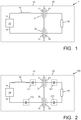
- FIG. 1 is a block diagram schematically illustrating a capacitive driving system 1, comprising a supply device 10 and a separate load device 20.
- the supply device 10 comprises two plate-shaped transmission electrodes 11, 12, which can be considered as output terminals.
- the supply device 10 further comprises a power generator 13 for generating AC power.
- a first output terminal 14 of the supply device 10 is connected to a first one 11 of the transmission electrodes, while a second output terminal 15 of the supply device 10 is connected to a second one 12 of the transmission electrodes.
- At least one inductor 16 is connected in series between the supply device 10 and the transmission electrodes 11, 12.
- the load device 20 comprises at least one load member 23 connected in series in between a first plate-shaped receiver electrode 21 and a second plate-shaped receiver electrode 22.
- the load member 23 is depicted as a resistor, and may ideally have ohmic characteristics.
- the transmission electrodes 11, 12 are located close to an outer surface of the supply device 10, and the receiver electrodes 21, 22 are located close to an outer surface of the load device 20.
- the disposition of the receiver electrodes 21, 22 matches the disposition of the transmission electrodes 11, 12, so that the load device 20 and the supply device 10 can be placed in close proximity of each other in an energy transfer position in which the first transmission electrode 11 together with the first receiver electrode 21 defines a first transfer capacitor 31 while simultaneously the second transmission electrode 12 together with the second receiver electrode 22 defines a second transfer capacitor 32.
- the inductor 16 together with the capacitors 31 and 32 define a resonance circuit having a resonance frequency, and the power generator 13 is designed to generate an AC output signal at said resonance frequency, so that the circuit operates in resonance and power is efficiently transferred from the power generator 13 to the load member 23.
- US 2009/302690 A1 discloses a power transmission system that includes a power supplying apparatus and a power receiving apparatus.
- the power supplying apparatus comprises a power generator, a first resonance unit and power supplying electrodes.
- the first resonance unit comprises an induction component and/or a capacitance component and resonates the power signal, which resonated power signal is externally radiated by the power supplying electrodes.
- the power receiving apparatus comprises power receiving electrodes for receiving the radiated power signal and a second resonance unit that has an induction component and/or a capacitance component.
- the power supplying electrodes and the power receiving electrodes define transfer capacitors.
- the control unit controls the induction component and/or a capacitance component of the first or the second resonance unit based on the power value measured by the power measurement unit. This is a rather complicated way to compensate for spatial or placement deviations.
- a general objective of the present invention is to eliminate or at least reduce the above-mentioned problems.
- At least one auxiliary capacitance is included in series with the transfer capacitors, either included in the supply device or in the load device, or both.
- the auxiliary capacitance is preferably designed to have a lower capacitance value than the optimum design capacitance of the transfer capacitors, and is preferably manufactured to a precision better than the expected variation of the transfer capacitors. Consequently, the resonance properties of the system are primarily determined by the auxiliary capacitance, so that the accuracy of the system as a whole has improved.
- FIG. 2 is a block diagram comparable to figure 1 , of a capacitive driving system 100 illustrating the basic principle underlying the present invention.
- the figure shows four possible locations for an auxiliary capacitance included in series with the transfer capacitors 31, 32.
- a first auxiliary capacitance 111 is shown at a first possible location in the supply device 10, in series with the first transmission electrode 11 and the inductor 16.
- a second auxiliary capacitance 112 is shown at a second possible location in the supply device 10, in series with the generator's opposite output 15 and the second transmission electrode 12.
- a third auxiliary capacitance 121 is shown at a first possible location in the load device 20, in between the load 23 and the first receiver electrode 21.
- a fourth auxiliary capacitance 122 is shown at a second possible location in the load device 20, in between the load 23 and the second receiver electrode 22. It should be clear that, in each and every one of the above examples, in the resonant circuit going from the first output terminal 14 of the supply device 10 to the opposite output terminal.
- the auxiliary capacitance concerned is arranged in series with the transfer capacitances.
- the invention can be implemented with any one of the auxiliary capacitances shown, but it is also possible to have a combination with two (or more) auxiliary capacitances in the supply device 10, two (or more) auxiliary capacitances in the load device 20, at one side or at opposite sides of the load, or one (or more) auxiliary capacitances in the supply device 10 and one (or more) auxiliary capacitances in the load device 20.
- the transfer capacitors 31, 32 each have a design capacitance C1 and a variation ⁇ 1, meaning that this capacitance can range from (1- ⁇ 1) ⁇ C1 to (1+ ⁇ 1) ⁇ C1.
- one auxiliary capacitance 121 in series with the load having a design capacitance Ca and a variation ⁇ a.
- Ca / C 1 x , with x ⁇ 1.
- ⁇ a / ⁇ 1 y , with y ⁇ 1.
- FIG 3 is a block diagram of a capacitive driving system 300 adapted for driving multiple loads.
- the supply device now indicated by reference numeral 310, has multiple sets of transmission electrodes 311, 312. In Figure 3 , four such sets are shown, but the number of sets may be higher or lower than four.
- Each set of electrodes is capable of coupling to a load device 320, always comprising a load member 323 in series with receiver electrodes 321, 322.
- FIG 3 only three load devices are shown. In the following, if it is intended to distinguish individual load devices and corresponding electrodes, characters A, B, C etc. will be added to the reference numerals.
- the supply device 310 can accommodate any number of load devices up to a certain maximum number. It is not necessary that all transmission electrodes are occupied. In figure 3 , transmission electrodes 311B, 312B are free.
- respective auxiliary capacitances 340 are arranged in series with the respective transmission electrodes 311. It is noted that such auxiliary capacitances 350 may, additionally or alternatively, also be arranged in series with the respective opposite transmission electrodes 312, as shown.
- auxiliary capacitances 340 and/or 350 are auxiliary capacitances dedicated to individual transmission electrodes.
- Figure 3 further shows that it is also possible to have, additionally or alternatively, one or more common auxiliary capacitances 361, 362 in series with one or more of the output terminals 14, 15 of the power generator 13.
- the various transmission electrodes are actually discrete electrodes: it is for instance possible that the transmission electrodes are implemented as continuous strips 411, 412, allowing one or more load devices, now indicated by reference numeral 420, to be coupled to any surface portion of such relatively large-surface electrode.
- Such system 400 is schematically illustrated in Figure 4 .
- the supply device 410 has one common auxiliary capacitance 461 in series with the inductance 16 and/or one common auxiliary capacitance 462 in series with the opposite output terminal 15 of the power generator 13.
- the auxiliary capacitance(s) is/are arranged in the supply device 310, 410.
- Such system 300, 400 is particularly useful in cases where one or more users can add one or more load devices as desired.
- Exemplary embodiments of such systems are: a charging system for mobile devices such as telephones, PDAs, laptops, etc; an illumination system where lamp units can be added and placed as desired.
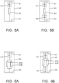
- FIG. 5A An example of such load device 520 according to the present invention is schematically illustrated in Figure 5A .
- the load device 520 comprises a load member 523 connected in series between two plate-shaped receiver electrodes 521, 522.
- a small auxiliary capacitance 540 is connected in series with the load 523.
- two such small auxiliary capacitances 541, 542 can be arranged at opposite sides of the load member 523, as shown in Figure 5B .
- This load device 520 can be used in cooperation with a supply device 10 of Figure 1 .
- FIG. 6A shows an embodiment of a load device 620 according to the present invention, comprising two loads 623A and 623B connected in parallel, this parallel circuit being connected in series between two plate-shaped receiver electrodes 621, 622.
- a small common auxiliary capacitance 640 is connected in series with the parallel arrangement of loads 623A and 623B.
- two such small auxiliary capacitances 641, 642 can be arranged in series at opposite sides of said parallel circuit of load members 623A, 623B, as shown in Figure 6B .
- said parallel circuit may comprise more than two load members connected in parallel, with always one or more common auxiliary capacitance(s) connected in series with the parallel circuit.
- FIG. 7 shows an embodiment of a load device 720 according to the present invention, comprising two load members 723A and 723B connected in parallel, this parallel circuit being connected in series between two plate-shaped receiver electrodes 721, 722.
- small dedicated auxiliary capacitances 741 and 742 are connected in series with the respective load members 723A and 723B.
- the load device may have more than two loads connected in parallel, each load provided with its own dedicated auxiliary capacitance in series.
- each load member may be connected in series to two auxiliary capacitances at opposite sides, but this is not shown for sake of simplicity.
- Figure 8 shows an embodiment of a load device 820 according to the present invention, where the load device is an illumination device and comprises a load 823 of two (or more) strings of LEDs connected in series between two plate-shaped receiver electrodes 821, 822, each string comprising one or more LEDs, and the two strings being arranged anti-parallel to each other.
- the strings have one common auxiliary capacitance 840, but it is also possible to have individual dedicated auxiliary capacitance per LED string, comparable to Figure 7 .
- an accurate capacitance for the purposes of the present invention, it is useful to turn to semiconductor technology.
- Methods for manufacturing a capacitance in an integrated circuit are known per se. This is particularly useful in case the load device is an illumination device and comprises a plurality of LEDs. These LEDs may be manufactured in one semiconductor chip that also comprises individual capacitances per LED ( Figure 7 ) and/or common capacitances, in series with the LEDs.
- FIG. 9 is a block diagram schematically illustrating such building component 900.
- This building component 900 comprises, formed in one common semiconductor substrate 901, an anti-parallel arrangement of two LEDs 923, or a multiplicity thereof.
- the building component 900 comprises at least one common capacitance in series with said anti-parallel arrangement of LEDs.
- the arrangement is symmetrical and comprises two common capacitances 941, 942 at opposite sides of the said parallel arrangement of LEDs. It is also possible to have individual memori-capacitances per LED.
- a capacitive driving system that comprises:
- Either the supply device or the load device, or both comprise at least one inductor connected in series with at least one of said respective electrodes.
- the supply device and the load device have an energy transfer position in which a first one of said transmission electrodes together with a first one of said receiver electrodes defines a first transfer capacitor while simultaneously a second one of said transmission electrodes together with a second one of said receiver electrodes defines a second transfer capacitor.
- At least one auxiliary capacitance is connected in series with the inductor and the load member.
- the supply device comprises two or even more inductors, it is possible that the inductor is or multiple inductors are located in the load device, and it is possible that one or more inductor(s) is/are located in the supply device while simultaneously one or more inductor(s) is/are located in the load device.
- the key of the invention is the presence of at least one series capacitance in either the supply device or the load device, or both, the present invention also relates to a supply device comprising at least one series capacitance but not necessarily comprising an inductor, and the present invention also relates to a load device comprising at least one series capacitance but not necessarily comprising an inductor.
- an illumination load device comprises two LEDs (or LED strings) arranged anti-parallel.
- Such anti-parallel arrangement allows for either polarity of the resonant current to flow through one of the two branches.
- the other of said paths does not need to include any LEDs, but may for instance include one or more normal (i.e.
- the device as a whole remains an illumination device, albeit perhaps with less illumination efficiency.
- the second path may even be provided by an internal breakdown voltage of the LED itself, or by an internal protection diode of the LED itself.
Description
- The present invention relates in general to the field of wireless power transfer to a load device. In a particular embodiment, the load device is a lighting device including one or more light-generating units. In another example, the transfer involves the charging of a battery of an appliance, for instance a telephone. The invention will be specifically explained for these examples without intending to limit the scope of the invention to these examples.
- Traditionally, electric power from a source to a load is transferred via wires, which obviously requires that the load device is connected to the source via wires. The desire to be able to move the load device leads to the solution of having connectors in the wires, such connectors making mechancial (Ohmic) contact. There are however examples where it is desirable to move the load device often, in which case the need to often connect/disconnect such connector becomes a burden. Practical examples include electric toothbrushes, telephones, and also lamps. To meet such desire, wireless power transfer has been developed. In such devices, connectors involve an inductive or a capacitive coupling. Typically, one of the coupling components is arranged within or attached to the housing of the load device itself. For instance, in the case of inductive coupling, the housing of the load device may contain a receiver coil, which for power transfer will be coupled to a transmission coil in a docking station, the two coupled coils basically constitute a transformer. In the case of capacitive coupling, the load device will include at least one receiver electrode which for power transfer will be coupled capacitively to a transmission electrode in a supply structure such as for instance a docking station. Such receiver electrode and transmission electrode are usually implemented as a plate, and when coupled they together define a capacitor.
-
Figure 1 is a block diagram schematically illustrating acapacitive driving system 1, comprising asupply device 10 and aseparate load device 20. Thesupply device 10 comprises two plate-shaped transmission electrodes supply device 10 further comprises apower generator 13 for generating AC power. Afirst output terminal 14 of thesupply device 10 is connected to a first one 11 of the transmission electrodes, while asecond output terminal 15 of thesupply device 10 is connected to a second one 12 of the transmission electrodes. At least oneinductor 16 is connected in series between thesupply device 10 and thetransmission electrodes load device 20 comprises at least oneload member 23 connected in series in between a first plate-shaped receiver electrode 21 and a second plate-shaped receiver electrode 22. Theload member 23 is depicted as a resistor, and may ideally have ohmic characteristics. Thetransmission electrodes supply device 10, and thereceiver electrodes load device 20. The disposition of thereceiver electrodes transmission electrodes load device 20 and thesupply device 10 can be placed in close proximity of each other in an energy transfer position in which thefirst transmission electrode 11 together with thefirst receiver electrode 21 defines afirst transfer capacitor 31 while simultaneously thesecond transmission electrode 12 together with thesecond receiver electrode 22 defines asecond transfer capacitor 32. - The
inductor 16 together with thecapacitors power generator 13 is designed to generate an AC output signal at said resonance frequency, so that the circuit operates in resonance and power is efficiently transferred from thepower generator 13 to theload member 23. - There are applications where the
load device 20 is mounted to thesupply device 10 once, and there are applications where theload device 20 is connected to and disconnected from thesupply device 10 frequently. In any case, there exists a problem that the precise actual capacitance value of thetransfer capacitors load device 20. A displacement of theload device 20 with respect to thesupply device 10, or the accidental presence of pieces of dirt between the contacts, or, in cases where an additional dielectric contact liquid is applied, variations in the properties of the dielectric, will result in variation of the actual capacitance value of thetransfer capacitors power generator 13 is set to operate at the design resonance frequency, a variation in the power transferred to theload member 23. - Such variation is undesirable, with the level of inconvenience depending on the situation. In the case of a charger of an appliance, charging to the required level can take longer than expected, or the batteries are charged insufficiently and will be exhausted before this is expected. In case multiple mutually identical loads are driven in parallel, the loads receive different amounts of power. In the case of a lighting system having multiple lighting units driven in parallel, the respective lighting units produce mutually different output light levels, which is clearly visible to an observer.
- For the developer and manufacturer of the driving system, such possible variations mean that there is uncertainty about the actual capacitance value of the
transfer capacitors -
US 2009/302690 A1 discloses a power transmission system that includes a power supplying apparatus and a power receiving apparatus. The power supplying apparatus comprises a power generator, a first resonance unit and power supplying electrodes. The first resonance unit comprises an induction component and/or a capacitance component and resonates the power signal, which resonated power signal is externally radiated by the power supplying electrodes. The power receiving apparatus comprises power receiving electrodes for receiving the radiated power signal and a second resonance unit that has an induction component and/or a capacitance component. The power supplying electrodes and the power receiving electrodes define transfer capacitors. To transmit power more efficiently by relaxing constraints on spatial relationships the power transmission system is provided with a control unit. The control unit controls the induction component and/or a capacitance component of the first or the second resonance unit based on the power value measured by the power measurement unit. This is a rather complicated way to compensate for spatial or placement deviations. - A general objective of the present invention is to eliminate or at least reduce the above-mentioned problems.
- According to an important aspect of the present invention, at least one auxiliary capacitance is included in series with the transfer capacitors, either included in the supply device or in the load device, or both. The auxiliary capacitance is preferably designed to have a lower capacitance value than the optimum design capacitance of the transfer capacitors, and is preferably manufactured to a precision better than the expected variation of the transfer capacitors. Consequently, the resonance properties of the system are primarily determined by the auxiliary capacitance, so that the accuracy of the system as a whole has improved.
- Further advantageous elaborations are mentioned in the dependent claims.
- These and other aspects, features and advantages of the present invention will be further explained by the following description of one or more preferred embodiments with reference to the drawings, in which same reference numerals indicate same or similar parts, and in which:
-
Fig. 1 is a block diagram schematically illustrating a capacitive driving system; -
Fig. 2 is a block diagram schematically illustrating a capacitive driving system; -
Fig. 3 is a block diagram schematically illustrating a capacitive driving system for driving multiple loads; -
Fig. 4 is a block diagram schematically illustrating a capacitive driving system for driving multiple loads; -
Figs. 5A and 5B are block diagrams schematically illustrating examples of a load device capable of being capacitively driven; -
Figs. 6A and 6B are block diagrams schematically illustrating other examples of a load device capable of being capacitively driven; -
Fig. 7 is a block diagram schematically illustrating another example of a load device capable of being capacitively driven; -
Fig. 8 is a block diagram schematically illustrating another example of a load device capable of being capacitively driven; -
Fig. 9 is a block diagram schematically illustrating a semiconductor building component. -
Figure 2 is a block diagram comparable tofigure 1 , of acapacitive driving system 100 illustrating the basic principle underlying the present invention. The figure shows four possible locations for an auxiliary capacitance included in series with thetransfer capacitors auxiliary capacitance 111 is shown at a first possible location in thesupply device 10, in series with thefirst transmission electrode 11 and theinductor 16. A secondauxiliary capacitance 112 is shown at a second possible location in thesupply device 10, in series with the generator'sopposite output 15 and thesecond transmission electrode 12. A thirdauxiliary capacitance 121 is shown at a first possible location in theload device 20, in between theload 23 and thefirst receiver electrode 21. A fourthauxiliary capacitance 122 is shown at a second possible location in theload device 20, in between theload 23 and thesecond receiver electrode 22. It should be clear that, in each and every one of the above examples, in the resonant circuit going from thefirst output terminal 14 of thesupply device 10 to the opposite output terminal. The auxiliary capacitance concerned is arranged in series with the transfer capacitances. The invention can be implemented with any one of the auxiliary capacitances shown, but it is also possible to have a combination with two (or more) auxiliary capacitances in thesupply device 10, two (or more) auxiliary capacitances in theload device 20, at one side or at opposite sides of the load, or one (or more) auxiliary capacitances in thesupply device 10 and one (or more) auxiliary capacitances in theload device 20. - For explaining the invention, the following calculation is given.
- Assume that the
transfer capacitors auxiliary capacitance 121 in series with the load, having a design capacitance Ca and a variation Δa.

- It will be seen that the overall capacitance Ct of the circuit can be written as

- The smaller the ratio x, the more accurate the above approximation is. In practice, x can easily be smaller than 0.01.
- From the same equation, it can be seen that the variation in the overall capacitance Ct is primarily determined by the variation Δa of the auxiliary capacitance. Consequently, the resonance frequency of the system is now more accurate, and is less sensitive to variations in the capacitance of the
transfer capacitors -
Figure 3 is a block diagram of acapacitive driving system 300 adapted for driving multiple loads. The supply device, now indicated byreference numeral 310, has multiple sets of transmission electrodes 311, 312. InFigure 3 , four such sets are shown, but the number of sets may be higher or lower than four. Each set of electrodes is capable of coupling to aload device 320, always comprising aload member 323 in series withreceiver electrodes Figure 3 , only three load devices are shown. In the following, if it is intended to distinguish individual load devices and corresponding electrodes, characters A, B, C etc. will be added to the reference numerals. - The
supply device 310 can accommodate any number of load devices up to a certain maximum number. It is not necessary that all transmission electrodes are occupied. Infigure 3 ,transmission electrodes - According to the invention, respective auxiliary capacitances 340 are arranged in series with the respective transmission electrodes 311. It is noted that such auxiliary capacitances 350 may, additionally or alternatively, also be arranged in series with the respective opposite transmission electrodes 312, as shown.
- The auxiliary capacitances 340 and/or 350 are auxiliary capacitances dedicated to individual transmission electrodes.
Figure 3 further shows that it is also possible to have, additionally or alternatively, one or more commonauxiliary capacitances output terminals power generator 13. - It is noted that it is not necessary that the various transmission electrodes are actually discrete electrodes: it is for instance possible that the transmission electrodes are implemented as
continuous strips Such system 400 is schematically illustrated inFigure 4 . In this case, thesupply device 410 has one commonauxiliary capacitance 461 in series with theinductance 16 and/or one commonauxiliary capacitance 462 in series with theopposite output terminal 15 of thepower generator 13. - In the driving
systems Figures 3 and4 , the auxiliary capacitance(s) is/are arranged in thesupply device Such system - In another approach, it is possible to adapt a load device for cooperation with a capacitive supply device that does not need to be adapted. Such solution is particularly useful in cases where it is undesirable or even impossible to adapt the supply device, for instance in the case of an existing supply device. An example of
such load device 520 according to the present invention is schematically illustrated inFigure 5A . Again, theload device 520 comprises aload member 523 connected in series between two plate-shapedreceiver electrodes auxiliary capacitance 540 is connected in series with theload 523. In a symmetric device, two such smallauxiliary capacitances load member 523, as shown inFigure 5B . Thisload device 520 can be used in cooperation with asupply device 10 ofFigure 1 . -
Figure 6A shows an embodiment of aload device 620 according to the present invention, comprising twoloads receiver electrodes auxiliary capacitance 640 is connected in series with the parallel arrangement ofloads auxiliary capacitances load members Figure 6B . It is noted that said parallel circuit may comprise more than two load members connected in parallel, with always one or more common auxiliary capacitance(s) connected in series with the parallel circuit. -
Figure 7 shows an embodiment of aload device 720 according to the present invention, comprising twoload members receiver electrodes auxiliary capacitances respective load members - It is noted that a combination of dedicated auxiliary capacitances and common auxiliary capacitance is also possible.
-
Figure 8 shows an embodiment of aload device 820 according to the present invention, where the load device is an illumination device and comprises aload 823 of two (or more) strings of LEDs connected in series between two plate-shapedreceiver electrodes figure 6 , the strings have one commonauxiliary capacitance 840, but it is also possible to have individual dedicated auxiliary capacitance per LED string, comparable toFigure 7 . - For manufacturing an accurate capacitance for the purposes of the present invention, it is useful to turn to semiconductor technology. Methods for manufacturing a capacitance in an integrated circuit are known per se. This is particularly useful in case the load device is an illumination device and comprises a plurality of LEDs. These LEDs may be manufactured in one semiconductor chip that also comprises individual capacitances per LED (
Figure 7 ) and/or common capacitances, in series with the LEDs. - The present invention is also embodied in a semiconductor building component that is particularly suitable for building illumination load devices suitable for being driven capacitively.
Figure 9 is a block diagram schematically illustratingsuch building component 900. Thisbuilding component 900 comprises, formed in onecommon semiconductor substrate 901, an anti-parallel arrangement of twoLEDs 923, or a multiplicity thereof. Formed in thesame substrate 901, thebuilding component 900 comprises at least one common capacitance in series with said anti-parallel arrangement of LEDs. In the embodiment shown, the arrangement is symmetrical and comprises twocommon capacitances - Summarizing, the present invention provides a capacitive driving system that comprises:
- a supply device comprising a power generator and capacitive transmission electrodes coupled to said power generator;
- at least one load device comprising two capacitive receiver electrodes and at least one load member coupled to said receiver electrodes.
- Either the supply device or the load device, or both, comprise at least one inductor connected in series with at least one of said respective electrodes.
- For resonant energy transfer, the supply device and the load device have an energy transfer position in which a first one of said transmission electrodes together with a first one of said receiver electrodes defines a first transfer capacitor while simultaneously a second one of said transmission electrodes together with a second one of said receiver electrodes defines a second transfer capacitor.
- At least one auxiliary capacitance is connected in series with the inductor and the load member.
- While the invention has been illustrated and described in detail in the drawings and foregoing description, it should be clear to a person skilled in the art that such illustration and description are to be considered illustrative or exemplary and not restrictive. The invention is not limited to the disclosed embodiments; rather, several variations and modifications are possible within the protective scope of the invention as defined in the appending claims.
- For instance, instead of one inductor being located exclusively in the supply device, it is possible that the supply device comprises two or even more inductors, it is possible that the inductor is or multiple inductors are located in the load device, and it is possible that one or more inductor(s) is/are located in the supply device while simultaneously one or more inductor(s) is/are located in the load device. Since the key of the invention is the presence of at least one series capacitance in either the supply device or the load device, or both, the present invention also relates to a supply device comprising at least one series capacitance but not necessarily comprising an inductor, and the present invention also relates to a load device comprising at least one series capacitance but not necessarily comprising an inductor.
- Further, in the embodiments illustrated in
figures 8 and 9 , an illumination load device comprises two LEDs (or LED strings) arranged anti-parallel. Such anti-parallel arrangement allows for either polarity of the resonant current to flow through one of the two branches. However, to achieve this effect, it is not necessary to have two anti-parallel (strings of) LEDs: it is sufficient to have a first current path for first polarity current and to have a second path for opposite polarity current while at least one of these paths includes at least one LED. The other of said paths does not need to include any LEDs, but may for instance include one or more normal (i.e. non-emissive) diodes or a simple resistor; the device as a whole remains an illumination device, albeit perhaps with less illumination efficiency. Depending on the LED technology used, the second path may even be provided by an internal breakdown voltage of the LED itself, or by an internal protection diode of the LED itself. - Other variations to the disclosed embodiments can be understood and effected by those skilled in the art in practicing the claimed invention, from a study of the drawings, the disclosure, and the appended claims. In the claims, the word "comprising" does not exclude other elements or steps, and the indefinite article "a" or "an" does not exclude a plurality. Even if certain features are recited in different dependent claims, the present invention also relates to an embodiment comprising these features in common. Any reference signs in the claims should not be construed as limiting the scope.
Claims (12)
- Capacitive driving system (100), comprising:- a supply device (10), the supply device (10) comprising a power generator (13) having two output terminals (14, 15), at least one set of capacitive transmission electrodes (11, 12) coupled to respective ones of the output terminals (14, 15);- at least one load device (20), the load device (20) comprising two capacitive receiver electrodes (21, 22) and at least one load member (23) coupled to said receiver electrodes (21, 22);wherein at least one of the supply device (10) and the load device (20) comprise at least one inductor (16) connected in series with at least one of said respective electrodes (11, 12; 21, 22);
wherein the supply device (10) and the load device (20) have an energy transfer position in which a first one of said transmission electrodes (11) together with a first one of said receiver electrodes (21) defines a first transfer capacitor (31) while simultaneously a second one of said transmission electrodes (12) together with a second one of said receiver electrodes (22) defines a second transfer capacitor (32);
wherein, in the energy transfer position, resonant energy transfer takes place from the supply device (10) to the load member (23);
wherein, in the resonant circuit containing the at least one inductor (16) and the load member (23) in the energy transfer position, at least one auxiliary capacitance (111; 112; 121; 122) is connected in series with the inductor (16) and the load member (23);
wherein the capacitance value of each one of said transfer capacitors (31, 32) is in a range from (1-Δ1)·C1 to (1+Δ1)·C1, in which C1 is indicated as design capacitance of the transfer capacitors and in which Δ1 is indicated as variation of the transfer capacitors;
wherein the capacitance value of the auxiliary capacitance is in a range from (1-Δa)·Ca to (1+Δa)·Ca, in which Ca is indicated as design capacitance of the auxiliary capacitance and in which Δa is indicated as variation of the auxiliary capacitance;
and wherein Ca < C1 applies and wherein Δa < Δ1 applies. - Capacitive driving system according to claim 1, wherein the supply device (10) comprises at least one inductor (16) connected in series between the power generator (13) and at least one of said transmission electrodes (11, 12).
- Capacitive supply device (10) adapted for a capacitive driving system according to claim 1, comprising a power generator (13) having two output terminals (14, 15), at least one set of capacitive transmission electrodes (11, 12) coupled to respective ones of the output terminals (14, 15) and at least one auxiliary capacitance (111; 112) connected in series with at least one of said transmission electrodes (11, 12);
said transmission electrodes (11, 12) designed and suited for capacitive coupling with two capacitive receiver electrodes (21, 22) of a load device (20) adapted for a capacitive driving system according to claim 1, the coupled transmission and receiver electrodes defining transfer capacitors;
the supply device (10) preferably further comprising at least one inductor (16) connected in series between the power generator (13) and at least one of said transmission electrodes (11, 12);
wherein the capacitance value of each one of said transfer capacitors is in a range from (1-Δ1)·C1 to (1+Δ1)·C1, in which C1 is indicated as design capacitance of the transfer capacitors and in which Δ1 is indicated as variation of the transfer capacitors;
wherein the capacitance value of the auxiliary capacitance is in a range from (1-Δa)·Ca to (1+Δa)·Ca, in which Ca is indicated as design capacitance of the auxiliary capacitance and in which Δa is indicated as variation of the auxiliary capacitance;
and wherein Ca < C1 applies and wherein Δa < Δ1 applies. - Capacitive supply device (310) according to claim 3, comprising a plurality of capacitive transmission electrodes (311, 312) coupled to said output terminals (14, 15), further comprising respective auxiliary capacitances (340; 350) connected in series with the respective transmission electrodes (311, 312).
- Capacitive supply device (410) according to claim 3, comprising at least two relatively large capacitive transmission electrodes (411, 412) coupled to said output terminals (14, 15) designed and suited for capacitive coupling with capacitive receiver electrodes (421, 422) of a plurality of load devices (420) that further each comprise at least one load member (423) coupled to said receiver electrodes (421, 422);
the supply device (410) further comprising at least one auxiliary capacitance (461; 462) connected in series with a respective transmission electrode (411,412). - Capacitive load device (20) adapted for a capacitive driving system according to claim 1, comprising two capacitive receiver electrodes (21, 22), at least one load member (23) coupled to said receiver electrodes (21, 22) and at least one auxiliary capacitance (121; 122) connected in series with the load member (23) and/or connected in series with at least one of said receiver electrodes (21, 22);
wherein said receiver electrodes (21, 22) are designed and suited for capacitive coupling with two capacitive transmission electrodes (11, 12) of a supply device (10) adapted for the capacitive driving system according to claim 1, the coupled transmission and receiver electrodes defining transfer capacitors, and preferably at least one inductor (16) connected in series between the power generator (13) and at least one of said transmission electrodes (11, 12);
wherein the capacitance value of each one of said transfer capacitors is in a range from (1-Δ1)·C1 to (1+Δ1)·C1, in which C1 is indicated as design capacitance of the transfer capacitors and in which Δ1 is indicated as variation of the transfer capacitors;
wherein the capacitance value of the auxiliary capacitance is in a range from (1-Δa)·Ca to (1+Δa)·Ca, in which Ca is indicated as design capacitance of the auxiliary capacitance and in which Δa is indicated as variation of the auxiliary capacitance;
and wherein Ca < C1 applies and wherein Δa < Δ1 applies. - Capacitive load device (520) according to claim 6, comprising two auxiliary capacitances (541; 542) connected in series at opposite ends of the load member (23).
- Capacitive load device (620) according to claim 6, comprising a parallel arrangement of at least two load members (623A, 623B) and one common auxiliary capacitance (640) connected in series with said parallel arrangement.
- Capacitive load device (620) according to claim 6, comprising a parallel arrangement of at least two load members (623A, 623B) and two auxiliary capacitances (641; 642) connected in series at opposite ends of said parallel arrangement.
- Capacitive load device (720) according to claim 6, comprising a parallel arrangement of at least two load members (723A, 723B) and respective individual auxiliary capacitances (741; 742) connected in series with respective ones of said load members.
- Capacitive load device (820) according to any of claims 8-10, wherein the load device is an illumination load device and at least one of said two load members comprises a string of at least one first LED, while the other one of said two load members is at least electrically conductive in the opposite direction as compared to the forward direction of said at least one first LED, said other one of said two load members preferably comprising a string of at least one LED arranged anti-parallel to said at least one first LED.
- Semiconductor building component (900) adapted for a capacitive driving system according to claim 1, comprising a common semiconductor substrate (901), at least one anti-parallel arrangement of strings of one or more LEDs (923) formed in said semiconductor substrate (901), and at least one auxiliary capacitance (941, 942) formed in said semiconductor substrate (901) and connected in series with said anti-parallel arrangement of LEDs, or connected in series with respective ones of said LED strings.
Priority Applications (1)
| Application Number | Priority Date | Filing Date | Title |
|---|---|---|---|
| EP14781566.6A EP3055918B1 (en) | 2013-10-09 | 2014-10-09 | System for capacitively driving a load |
Applications Claiming Priority (3)
| Application Number | Priority Date | Filing Date | Title |
|---|---|---|---|
| EP13187953 | 2013-10-09 | ||
| PCT/EP2014/071591 WO2015052263A1 (en) | 2013-10-09 | 2014-10-09 | System for capacitively driving a load |
| EP14781566.6A EP3055918B1 (en) | 2013-10-09 | 2014-10-09 | System for capacitively driving a load |
Publications (2)
| Publication Number | Publication Date |
|---|---|
| EP3055918A1 EP3055918A1 (en) | 2016-08-17 |
| EP3055918B1 true EP3055918B1 (en) | 2017-04-26 |
Family
ID=49484082
Family Applications (1)
| Application Number | Title | Priority Date | Filing Date |
|---|---|---|---|
| EP14781566.6A Not-in-force EP3055918B1 (en) | 2013-10-09 | 2014-10-09 | System for capacitively driving a load |
Country Status (5)
| Country | Link |
|---|---|
| US (1) | US9748801B2 (en) |
| EP (1) | EP3055918B1 (en) |
| JP (1) | JP2016538810A (en) |
| CN (1) | CN105637731A (en) |
| WO (1) | WO2015052263A1 (en) |
Families Citing this family (5)
| Publication number | Priority date | Publication date | Assignee | Title |
|---|---|---|---|---|
| CN105191061B (en) * | 2013-03-19 | 2017-11-14 | 株式会社村田制作所 | wireless power transmission system |
| JP6112235B2 (en) * | 2014-02-07 | 2017-04-12 | 株式会社村田製作所 | Power transmission system |
| DE102016105897A1 (en) * | 2016-03-31 | 2017-10-05 | Technische Universität Darmstadt | Apparatus and method for impressing an electric current |
| CN108964289B (en) * | 2018-07-23 | 2020-03-31 | 重庆大学 | ECPT system with double T-shaped resonant networks and parameter design method thereof |
| DE102019120428A1 (en) | 2019-07-29 | 2021-02-04 | Bayerische Motoren Werke Aktiengesellschaft | Energy transmission device for the wireless transmission of electrical energy, and method |
Family Cites Families (18)
| Publication number | Priority date | Publication date | Assignee | Title |
|---|---|---|---|---|
| US3273046A (en) * | 1961-05-08 | 1966-09-13 | Gen Electric | Inverter circuits with independent commutation circuits |
| JP2004511078A (en) * | 2000-10-13 | 2004-04-08 | フラット ホワイト ライティング ピーティーワイ リミテッド | Lighting system |
| JP2003345308A (en) * | 2002-05-29 | 2003-12-03 | Pioneer Electronic Corp | Display panel and display device |
| US7049754B2 (en) | 2004-07-06 | 2006-05-23 | Dell Products L.P. | System and method for reducing information handling system distributed capacitance |
| FR2876516A1 (en) * | 2004-10-11 | 2006-04-14 | Thomson Licensing Sa | AMPLIFIER FOR GENERATING A RECTANGULAR VOLTAGE SIGNAL WITH SWITCH SWITCHES ON A CAPACITIVE LOAD |
| JP4557049B2 (en) * | 2008-06-09 | 2010-10-06 | ソニー株式会社 | Transmission system, power supply apparatus, power reception apparatus, and transmission method |
| WO2009153715A2 (en) | 2008-06-17 | 2009-12-23 | Koninklijke Philips Electronics N.V. | Light emitting device adapted for ac drive |
| US20120091819A1 (en) | 2008-09-27 | 2012-04-19 | Konrad Kulikowski | Computer that wirelessly powers accessories |
| CN102754306B (en) * | 2010-05-28 | 2014-12-24 | 株式会社村田制作所 | Power transmission system |
| JP5093386B2 (en) * | 2010-08-25 | 2012-12-12 | 株式会社村田製作所 | Power transmission device and power transmission system |
| US8994223B2 (en) * | 2010-11-08 | 2015-03-31 | R2Z Innovations Inc. | Systems and methods for self powered electronic devices |
| WO2012120404A1 (en) * | 2011-03-07 | 2012-09-13 | Koninklijke Philips Electronics N.V. | Electroluminescent device |
| US8970069B2 (en) | 2011-03-28 | 2015-03-03 | Tdk Corporation | Wireless power receiver and wireless power transmission system |
| JP6096191B2 (en) * | 2011-08-16 | 2017-03-15 | フィリップス ライティング ホールディング ビー ヴィ | Transparent capacitive wireless power supply system |
| US9438129B2 (en) * | 2011-10-06 | 2016-09-06 | Cesar Ladron de Guevara | Input/output power and signal transfer isolator device |
| CN102508950B (en) * | 2011-10-14 | 2013-12-11 | 广东电网公司电力科学研究院 | Regional dispatching automatic system and method for communication between regional dispatching automatic system and remote monitoring diagnosis centre |
| JP2013158196A (en) * | 2012-01-31 | 2013-08-15 | Kyushu Univ | Transmitting system and power receiving device |
| JP2014135880A (en) * | 2013-01-11 | 2014-07-24 | Kyushu Univ | Transmission system, transmission device, reception device, and transmission method |
-
2014
- 2014-10-09 WO PCT/EP2014/071591 patent/WO2015052263A1/en active Application Filing
- 2014-10-09 US US15/027,693 patent/US9748801B2/en not_active Expired - Fee Related
- 2014-10-09 EP EP14781566.6A patent/EP3055918B1/en not_active Not-in-force
- 2014-10-09 CN CN201480055694.7A patent/CN105637731A/en active Pending
- 2014-10-09 JP JP2016520638A patent/JP2016538810A/en not_active Ceased
Non-Patent Citations (1)
| Title |
|---|
| None * |
Also Published As
| Publication number | Publication date |
|---|---|
| CN105637731A (en) | 2016-06-01 |
| WO2015052263A1 (en) | 2015-04-16 |
| US20160248274A1 (en) | 2016-08-25 |
| EP3055918A1 (en) | 2016-08-17 |
| JP2016538810A (en) | 2016-12-08 |
| US9748801B2 (en) | 2017-08-29 |
Similar Documents
| Publication | Publication Date | Title |
|---|---|---|
| EP3055918B1 (en) | System for capacitively driving a load | |
| EP2745379B1 (en) | A capacitive contactless powering system | |
| US11056919B2 (en) | Power transmission device and wireless power transmission system | |
| CN106410991B (en) | Foreign object detection device, wireless power transmission device, and wireless power transmission system | |
| CN102680125B (en) | Wireless temperature sensor | |
| US9698629B2 (en) | Wireless power transmission system, power transmitting device, and power receiving device | |
| JP2012186472A (en) | Power supply device and power reception/supply device | |
| US10084342B2 (en) | Transfer layer for wireless capacitive power | |
| EP2824678A1 (en) | Power supply device, power reception device, and power supply/reception device | |
| CN104254960A (en) | Wireless power receiving apparatus and power control method therefor | |
| US10033217B2 (en) | Wireless power receiver device, wireless power transmitter device, and wireless power transceiver device | |
| CN101854070A (en) | Battery charger | |
| KR20160030672A (en) | Wireless power receiving apparatus and wireless power transmitting and receiving system | |
| US20140339903A1 (en) | Electric power transmitting apparatus and method for controlling electric power transmission | |
| US20100317233A1 (en) | Electrical connection system | |
| US9673658B2 (en) | Non-contact capacitive coupling type power charging apparatus and non-contact capacitive coupling type battery apparatus | |
| US9899138B1 (en) | Coil structure for generating a uniform magnetic field and coil apparatus having the same | |
| KR20120008632A (en) | Apparatus for wireless charging battery with package chip and system thereof | |
| WO2007086673A1 (en) | Charging system for mobile devices | |
| US20150215007A1 (en) | Wireless power transmission system | |
| KR20110126428A (en) | Light emitting device | |
| KR101233785B1 (en) | Adc power supply system | |
| KR101229909B1 (en) | Apparatus for wireless charging battery with PCB-integrated type and system thereof | |
| WO2015052003A1 (en) | Wireless capacitive power receiving module | |
| JP2017028780A (en) | Wireless transmission device |
Legal Events
| Date | Code | Title | Description |
|---|---|---|---|
| PUAI | Public reference made under article 153(3) epc to a published international application that has entered the european phase |
Free format text: ORIGINAL CODE: 0009012 |
|
| 17P | Request for examination filed |
Effective date: 20160509 |
|
| AK | Designated contracting states |
Kind code of ref document: A1 Designated state(s): AL AT BE BG CH CY CZ DE DK EE ES FI FR GB GR HR HU IE IS IT LI LT LU LV MC MK MT NL NO PL PT RO RS SE SI SK SM TR |
|
| AX | Request for extension of the european patent |
Extension state: BA ME |
|
| REG | Reference to a national code |
Ref country code: DE Ref legal event code: R079 Ref document number: 602014009122 Country of ref document: DE Free format text: PREVIOUS MAIN CLASS: H02J0005000000 Ipc: H02J0050050000 |
|
| RIC1 | Information provided on ipc code assigned before grant |
Ipc: H02J 50/05 20160101AFI20161013BHEP |
|
| GRAP | Despatch of communication of intention to grant a patent |
Free format text: ORIGINAL CODE: EPIDOSNIGR1 |
|
| INTG | Intention to grant announced |
Effective date: 20161129 |
|
| DAX | Request for extension of the european patent (deleted) | ||
| GRAS | Grant fee paid |
Free format text: ORIGINAL CODE: EPIDOSNIGR3 |
|
| GRAA | (expected) grant |
Free format text: ORIGINAL CODE: 0009210 |
|
| AK | Designated contracting states |
Kind code of ref document: B1 Designated state(s): AL AT BE BG CH CY CZ DE DK EE ES FI FR GB GR HR HU IE IS IT LI LT LU LV MC MK MT NL NO PL PT RO RS SE SI SK SM TR |
|
| REG | Reference to a national code |
Ref country code: GB Ref legal event code: FG4D |
|
| REG | Reference to a national code |
Ref country code: CH Ref legal event code: EP |
|
| REG | Reference to a national code |
Ref country code: AT Ref legal event code: REF Ref document number: 888644 Country of ref document: AT Kind code of ref document: T Effective date: 20170515 |
|
| REG | Reference to a national code |
Ref country code: IE Ref legal event code: FG4D |
|
| REG | Reference to a national code |
Ref country code: DE Ref legal event code: R096 Ref document number: 602014009122 Country of ref document: DE |
|
| RIN2 | Information on inventor provided after grant (corrected) |
Inventor name: SEMPEL, ADRIANUS Inventor name: VAN DEN BIGGELAAR, THEODORUS JOHANNES PETRUS |
|
| REG | Reference to a national code |
Ref country code: NL Ref legal event code: MP Effective date: 20170426 |
|
| REG | Reference to a national code |
Ref country code: LT Ref legal event code: MG4D |
|
| REG | Reference to a national code |
Ref country code: AT Ref legal event code: MK05 Ref document number: 888644 Country of ref document: AT Kind code of ref document: T Effective date: 20170426 |
|
| PG25 | Lapsed in a contracting state [announced via postgrant information from national office to epo] |
Ref country code: NL Free format text: LAPSE BECAUSE OF FAILURE TO SUBMIT A TRANSLATION OF THE DESCRIPTION OR TO PAY THE FEE WITHIN THE PRESCRIBED TIME-LIMIT Effective date: 20170426 |
|
| PG25 | Lapsed in a contracting state [announced via postgrant information from national office to epo] |
Ref country code: AT Free format text: LAPSE BECAUSE OF FAILURE TO SUBMIT A TRANSLATION OF THE DESCRIPTION OR TO PAY THE FEE WITHIN THE PRESCRIBED TIME-LIMIT Effective date: 20170426 Ref country code: GR Free format text: LAPSE BECAUSE OF FAILURE TO SUBMIT A TRANSLATION OF THE DESCRIPTION OR TO PAY THE FEE WITHIN THE PRESCRIBED TIME-LIMIT Effective date: 20170727 Ref country code: LT Free format text: LAPSE BECAUSE OF FAILURE TO SUBMIT A TRANSLATION OF THE DESCRIPTION OR TO PAY THE FEE WITHIN THE PRESCRIBED TIME-LIMIT Effective date: 20170426 Ref country code: ES Free format text: LAPSE BECAUSE OF FAILURE TO SUBMIT A TRANSLATION OF THE DESCRIPTION OR TO PAY THE FEE WITHIN THE PRESCRIBED TIME-LIMIT Effective date: 20170426 Ref country code: FI Free format text: LAPSE BECAUSE OF FAILURE TO SUBMIT A TRANSLATION OF THE DESCRIPTION OR TO PAY THE FEE WITHIN THE PRESCRIBED TIME-LIMIT Effective date: 20170426 Ref country code: NO Free format text: LAPSE BECAUSE OF FAILURE TO SUBMIT A TRANSLATION OF THE DESCRIPTION OR TO PAY THE FEE WITHIN THE PRESCRIBED TIME-LIMIT Effective date: 20170726 Ref country code: HR Free format text: LAPSE BECAUSE OF FAILURE TO SUBMIT A TRANSLATION OF THE DESCRIPTION OR TO PAY THE FEE WITHIN THE PRESCRIBED TIME-LIMIT Effective date: 20170426 |
|
| REG | Reference to a national code |
Ref country code: FR Ref legal event code: PLFP Year of fee payment: 4 |
|
| PG25 | Lapsed in a contracting state [announced via postgrant information from national office to epo] |
Ref country code: BG Free format text: LAPSE BECAUSE OF FAILURE TO SUBMIT A TRANSLATION OF THE DESCRIPTION OR TO PAY THE FEE WITHIN THE PRESCRIBED TIME-LIMIT Effective date: 20170726 Ref country code: LV Free format text: LAPSE BECAUSE OF FAILURE TO SUBMIT A TRANSLATION OF THE DESCRIPTION OR TO PAY THE FEE WITHIN THE PRESCRIBED TIME-LIMIT Effective date: 20170426 Ref country code: PL Free format text: LAPSE BECAUSE OF FAILURE TO SUBMIT A TRANSLATION OF THE DESCRIPTION OR TO PAY THE FEE WITHIN THE PRESCRIBED TIME-LIMIT Effective date: 20170426 Ref country code: RS Free format text: LAPSE BECAUSE OF FAILURE TO SUBMIT A TRANSLATION OF THE DESCRIPTION OR TO PAY THE FEE WITHIN THE PRESCRIBED TIME-LIMIT Effective date: 20170426 Ref country code: IS Free format text: LAPSE BECAUSE OF FAILURE TO SUBMIT A TRANSLATION OF THE DESCRIPTION OR TO PAY THE FEE WITHIN THE PRESCRIBED TIME-LIMIT Effective date: 20170826 Ref country code: SE Free format text: LAPSE BECAUSE OF FAILURE TO SUBMIT A TRANSLATION OF THE DESCRIPTION OR TO PAY THE FEE WITHIN THE PRESCRIBED TIME-LIMIT Effective date: 20170426 |
|
| REG | Reference to a national code |
Ref country code: DE Ref legal event code: R097 Ref document number: 602014009122 Country of ref document: DE |
|
| PG25 | Lapsed in a contracting state [announced via postgrant information from national office to epo] |
Ref country code: SK Free format text: LAPSE BECAUSE OF FAILURE TO SUBMIT A TRANSLATION OF THE DESCRIPTION OR TO PAY THE FEE WITHIN THE PRESCRIBED TIME-LIMIT Effective date: 20170426 Ref country code: RO Free format text: LAPSE BECAUSE OF FAILURE TO SUBMIT A TRANSLATION OF THE DESCRIPTION OR TO PAY THE FEE WITHIN THE PRESCRIBED TIME-LIMIT Effective date: 20170426 Ref country code: DK Free format text: LAPSE BECAUSE OF FAILURE TO SUBMIT A TRANSLATION OF THE DESCRIPTION OR TO PAY THE FEE WITHIN THE PRESCRIBED TIME-LIMIT Effective date: 20170426 Ref country code: CZ Free format text: LAPSE BECAUSE OF FAILURE TO SUBMIT A TRANSLATION OF THE DESCRIPTION OR TO PAY THE FEE WITHIN THE PRESCRIBED TIME-LIMIT Effective date: 20170426 Ref country code: EE Free format text: LAPSE BECAUSE OF FAILURE TO SUBMIT A TRANSLATION OF THE DESCRIPTION OR TO PAY THE FEE WITHIN THE PRESCRIBED TIME-LIMIT Effective date: 20170426 |
|
| PGFP | Annual fee paid to national office [announced via postgrant information from national office to epo] |
Ref country code: FR Payment date: 20171031 Year of fee payment: 4 |
|
| PG25 | Lapsed in a contracting state [announced via postgrant information from national office to epo] |
Ref country code: IT Free format text: LAPSE BECAUSE OF FAILURE TO SUBMIT A TRANSLATION OF THE DESCRIPTION OR TO PAY THE FEE WITHIN THE PRESCRIBED TIME-LIMIT Effective date: 20170426 Ref country code: SM Free format text: LAPSE BECAUSE OF FAILURE TO SUBMIT A TRANSLATION OF THE DESCRIPTION OR TO PAY THE FEE WITHIN THE PRESCRIBED TIME-LIMIT Effective date: 20170426 |
|
| PLBE | No opposition filed within time limit |
Free format text: ORIGINAL CODE: 0009261 |
|
| STAA | Information on the status of an ep patent application or granted ep patent |
Free format text: STATUS: NO OPPOSITION FILED WITHIN TIME LIMIT |
|
| 26N | No opposition filed |
Effective date: 20180129 |
|
| PGFP | Annual fee paid to national office [announced via postgrant information from national office to epo] |
Ref country code: DE Payment date: 20171229 Year of fee payment: 4 |
|
| PG25 | Lapsed in a contracting state [announced via postgrant information from national office to epo] |
Ref country code: MC Free format text: LAPSE BECAUSE OF FAILURE TO SUBMIT A TRANSLATION OF THE DESCRIPTION OR TO PAY THE FEE WITHIN THE PRESCRIBED TIME-LIMIT Effective date: 20170426 |
|
| REG | Reference to a national code |
Ref country code: CH Ref legal event code: PL |
|
| REG | Reference to a national code |
Ref country code: IE Ref legal event code: MM4A |
|
| PG25 | Lapsed in a contracting state [announced via postgrant information from national office to epo] |
Ref country code: LU Free format text: LAPSE BECAUSE OF NON-PAYMENT OF DUE FEES Effective date: 20171009 Ref country code: LI Free format text: LAPSE BECAUSE OF NON-PAYMENT OF DUE FEES Effective date: 20171031 Ref country code: CH Free format text: LAPSE BECAUSE OF NON-PAYMENT OF DUE FEES Effective date: 20171031 |
|
| REG | Reference to a national code |
Ref country code: BE Ref legal event code: MM Effective date: 20171031 |
|
| PG25 | Lapsed in a contracting state [announced via postgrant information from national office to epo] |
Ref country code: BE Free format text: LAPSE BECAUSE OF NON-PAYMENT OF DUE FEES Effective date: 20171031 |
|
| PG25 | Lapsed in a contracting state [announced via postgrant information from national office to epo] |
Ref country code: MT Free format text: LAPSE BECAUSE OF NON-PAYMENT OF DUE FEES Effective date: 20171009 |
|
| PG25 | Lapsed in a contracting state [announced via postgrant information from national office to epo] |
Ref country code: IE Free format text: LAPSE BECAUSE OF NON-PAYMENT OF DUE FEES Effective date: 20171009 |
|
| REG | Reference to a national code |
Ref country code: DE Ref legal event code: R119 Ref document number: 602014009122 Country of ref document: DE |
|
| GBPC | Gb: european patent ceased through non-payment of renewal fee |
Effective date: 20181009 |
|
| PG25 | Lapsed in a contracting state [announced via postgrant information from national office to epo] |
Ref country code: HU Free format text: LAPSE BECAUSE OF FAILURE TO SUBMIT A TRANSLATION OF THE DESCRIPTION OR TO PAY THE FEE WITHIN THE PRESCRIBED TIME-LIMIT; INVALID AB INITIO Effective date: 20141009 |
|
| PG25 | Lapsed in a contracting state [announced via postgrant information from national office to epo] |
Ref country code: DE Free format text: LAPSE BECAUSE OF NON-PAYMENT OF DUE FEES Effective date: 20190501 |
|
| PG25 | Lapsed in a contracting state [announced via postgrant information from national office to epo] |
Ref country code: FR Free format text: LAPSE BECAUSE OF NON-PAYMENT OF DUE FEES Effective date: 20181031 |
|
| PG25 | Lapsed in a contracting state [announced via postgrant information from national office to epo] |
Ref country code: SI Free format text: LAPSE BECAUSE OF FAILURE TO SUBMIT A TRANSLATION OF THE DESCRIPTION OR TO PAY THE FEE WITHIN THE PRESCRIBED TIME-LIMIT Effective date: 20170426 |
|
| PG25 | Lapsed in a contracting state [announced via postgrant information from national office to epo] |
Ref country code: GB Free format text: LAPSE BECAUSE OF NON-PAYMENT OF DUE FEES Effective date: 20181009 Ref country code: CY Free format text: LAPSE BECAUSE OF FAILURE TO SUBMIT A TRANSLATION OF THE DESCRIPTION OR TO PAY THE FEE WITHIN THE PRESCRIBED TIME-LIMIT Effective date: 20170426 |
|
| PG25 | Lapsed in a contracting state [announced via postgrant information from national office to epo] |
Ref country code: MK Free format text: LAPSE BECAUSE OF FAILURE TO SUBMIT A TRANSLATION OF THE DESCRIPTION OR TO PAY THE FEE WITHIN THE PRESCRIBED TIME-LIMIT Effective date: 20170426 |
|
| PG25 | Lapsed in a contracting state [announced via postgrant information from national office to epo] |
Ref country code: TR Free format text: LAPSE BECAUSE OF FAILURE TO SUBMIT A TRANSLATION OF THE DESCRIPTION OR TO PAY THE FEE WITHIN THE PRESCRIBED TIME-LIMIT Effective date: 20170426 |
|
| PG25 | Lapsed in a contracting state [announced via postgrant information from national office to epo] |
Ref country code: PT Free format text: LAPSE BECAUSE OF FAILURE TO SUBMIT A TRANSLATION OF THE DESCRIPTION OR TO PAY THE FEE WITHIN THE PRESCRIBED TIME-LIMIT Effective date: 20170426 |
|
| PG25 | Lapsed in a contracting state [announced via postgrant information from national office to epo] |
Ref country code: AL Free format text: LAPSE BECAUSE OF FAILURE TO SUBMIT A TRANSLATION OF THE DESCRIPTION OR TO PAY THE FEE WITHIN THE PRESCRIBED TIME-LIMIT Effective date: 20170426 |