EP3055901B1 - Niederohmiger zirkulator - Google Patents
Niederohmiger zirkulator Download PDFInfo
- Publication number
- EP3055901B1 EP3055901B1 EP14792642.2A EP14792642A EP3055901B1 EP 3055901 B1 EP3055901 B1 EP 3055901B1 EP 14792642 A EP14792642 A EP 14792642A EP 3055901 B1 EP3055901 B1 EP 3055901B1
- Authority
- EP
- European Patent Office
- Prior art keywords
- port
- impedance
- circulator
- transformer
- different
- Prior art date
- Legal status (The legal status is an assumption and is not a legal conclusion. Google has not performed a legal analysis and makes no representation as to the accuracy of the status listed.)
- Active
Links
Images


Classifications
-
- H—ELECTRICITY
- H01—ELECTRIC ELEMENTS
- H01P—WAVEGUIDES; RESONATORS, LINES, OR OTHER DEVICES OF THE WAVEGUIDE TYPE
- H01P1/00—Auxiliary devices
- H01P1/32—Non-reciprocal transmission devices
- H01P1/38—Circulators
-
- H—ELECTRICITY
- H01—ELECTRIC ELEMENTS
- H01P—WAVEGUIDES; RESONATORS, LINES, OR OTHER DEVICES OF THE WAVEGUIDE TYPE
- H01P1/00—Auxiliary devices
- H01P1/32—Non-reciprocal transmission devices
- H01P1/38—Circulators
- H01P1/383—Junction circulators, e.g. Y-circulators
- H01P1/387—Strip line circulators
Definitions
- Example embodiments generally relate to microwave or radio frequency (RF) equipment and, more particularly, some embodiments relate to a circulator provided with at least one port having a different impedance than other ports of the circulator.
- RF radio frequency
- a circulator is a fundamental component of RF and microwave equipment such as, for example, transmitter multi-couplers that allow radio transmission sites to operate reasonably free of interference.
- Circulators such as ferrite circulators typically include at least three terminals or ports at which an external waveguide or transmission line connects to the circulator. A signal entering in any port can be transmitted only to the next port in rotation.
- a circulator is a three (or four) terminal, non-reciprocal device that permits RF or microwave energy to flow between two adjacent ports in only one direction.
- an isolator may be formed.
- the circulator may operate as an isolator, allowing signals to travel only in one direction between the two remaining ports.
- Impedance matching is an important consideration when connecting a circulator/isolator to external equipment.
- circulators/isolators have generally been provided with a junction impedance of 50 ohms.
- the provision of a stable and precise 50 ohm junction impedance for each port of the circulator/isolator, has been adopted as an industry standard so that each port can have a predictable impedance.
- a byproduct of this standard has been that in many cases, loads that may need to be served could have impedances of something other than 50 ohms.
- US2010/109791A1 refers to a circulator/isolator with an asymmetric resonator, wherein a center resonator is positioned between ferrite disks. There are two output ports of the circulator that are positioned 120° apart from each other. A third output port is positioned 120° apart from the other ports. Two ports have an impedance of 50 ohms and are connected to the center resonator through impedance transformation transmission lines. The bottom port is matched with a low impedance device.
- the center resonator has a deformed or eccentric portion that is employed to effect the desired impedance transformation to the lower impedance level. Hence, the geometry of the transmission line structure is varied to drive the impedance to a higher or lower value as needed.
- US2007/182504A1 refers to a nonreciprocal circuit device, such as an isolator or circulator, including a microstrip line member that has a connecting portion.
- the connecting portion includes three strip electrodes that radially extend from a central portion to radial positions corresponding to the periphery of the disk-shaped microwave ferrite member.
- the microstrip line member also includes branch lines that radially extend from the central portion between adjacent strip electrodes, and further includes low impedance lines that are connected to a tip end portion of each branch line.
- differently dimensioned low impedance lines are coupled to differently dimensioned output electrodes to form output ports of the device.
- US2001/017576A1 concerns an isolator device with a built-in power amplifier.
- a high frequency power amplifier circuit and an isolator element are connected with each other through circuit elements.
- the high power amplifier circuit and the isolator element are united with a single dielectric multilayered substrate.
- the isolator element has a first port that acts as an input port and preferably has an input impedance that is matched with the output impedance of the high frequency power amplifier circuit.
- the circulator element includes input port, output port and dummy port that are formed on the upper surface of the circulator element.
- US2004/155726A1 concerns transmission lines for high frequency electromagnetic signals wherein impedance matching the transmission lines is made by patterning a first dielectric material so that successively increasing dielectric constants are obtained without changing the width of the conductor.
- this patterning used for impedance matching wherein a conductor passes perpendicularly to the patterning of a bottom dielectric layer.
- the widths of the materials having different dielectric constants may be modified to produce a desired effective dielectric constant required for the impedance matching.
- Some example embodiments may provide an ability to enable designers to avoid the need to employ complicated cascading impedance transformations.
- example embodiments may enable designers to employ different junction impedances at different ports of a circulator. Some example embodiments may therefore improve the ability of designers to provide lower cost and less complex circulators that function well in environments where different loads may be encountered.
- a circulator is provided as defined in claim 1.
- a circulator may be configured to operate as an isolator.
- Circulators may also be configured to perform other functions such as, for example, duplexer functions, reflection amplifier functions and/or the like. Accordingly, descriptions herein will be provided in relation to describing a circulator. However, it should be appreciated that the descriptions are equally applicable to isolators or any other possible configuration of the circulator. Moreover, it should also be appreciated that although an example embodiment will be described herein in the context of a three-port circulator, the concepts described herein are equally applicable to other configurations (e.g., a four-port circulator) that may have different numbers of ports.
- FIG. 1 illustrates a basic conceptual view of a basic circulator 10 that may be employed within a power amplifier context.
- the circulator 10 has three ports (e.g., a first port 30, second port 32, and third port 34), each of which employs a port impedance matching circuit (e.g., first port impedance matching circuit 40, second port impedance matching circuit 42 and third port impedance matching circuit 44).
- Each port is operably coupled to external circuitry (e.g., first external circuit 50, second external circuit 52 and third external circuit 54) that may operate as a source or load for various configurations. Power may enter into any one of the ports and exit through an adjacent port after circulating in the direction shown by arrows 60.
- an external magnetic field is applied to the circulator 10 to cancel out internal circulating currents other than the desired path for energy "circulation," as described in greater detail below.
- the circulator 10 may therefore be a useful device for selective coupling of different ports where isolation of ports not currently coupled is desired.
- the circulator 10 may be useful in connection with configuration such that one or more of the external circuits may operate as a power amplifier or any of a number of other devices used for RF or microwave applications.
- the first port impedance matching circuit 40, the second port impedance matching circuit 42 and the third port impedance matching circuit 44 would each be provided to present a stable and accurate 50 ohm impedance at the first port 30, the second port 32, and the third port 34, respectively.
- example embodiments enable the provision of at least one different impedance value on at least one of the ports.
- the first and second ports 30 and 32 may employ corresponding first and second port impedance matching circuits 40 and 42 that are configured to provide an impedance of 50 ohms to match the impedance of the corresponding first and second external circuits 50 and 52.
- the third port 34 may employ the third port impedance matching circuit 44 to have a 12.5 ohm impedance to match the impedance of the third external circuit 54.
- the term "different impedance value” or discussions regarding differences in impedance values should be understood to represent larger than mere de minimis differences between impedance values.
- differences in impedance values should be understood to represent noticeable and relatively significant changes in impedance values when the impedance value of one port is compared to the impedance value of another port.
- an impedance value may be considered to be “different” with as little as 1% difference for relatively large impedance values.
- one port impedance may be at least 10% different (i.e., 5 ohms). In other examples, the difference may be larger (e.g., 20%, 50% or more).
- impedance transformers are often realized by cascading multiple 90 degree lengths of transmission lines, avoiding the use of multiple quarter-wave transmission lines by employing an example embodiment can enable designers to achieve relatively significant size reductions.
- complication and cost of manufacturing circulators and the components in which the circulators function may also be reduced by employing example embodiments.
- Lower impedances of certain components such as large power transistors may therefore be coupled to the ports (e.g., as examples of the external circuitry) and can be accommodated with lower impedance values of the corresponding ports.
- FIG. 2 illustrates a three-dimensional view of a circulator 100 according to an example embodiment.
- the circulator 100 of FIG. 2 may be an example of the circulator 10 described in connection with FIG. 1 .
- the circulator 100 may include an upper ferrite puck 110 and a lower ferrite puck 112 that may be disposed on opposing sides of a transmission medium 120.
- the transmission medium 120 may extend in each of three directions that may be disposed substantially 120 degrees apart from each other.
- ends of the transmission medium 120 may be operably coupled to a first transformer 130, a second transformer 132 and a third transformer 134, respectively.
- the transmission medium 120 may be a substantially Y-shaped material formed as a conductive strip line or trace.
- the first transformer 130, the second transformer 132 and the third transformer 134 may each be disposed between an upper dielectric and a lower dielectric to form a component having a desired and predictable impedance.
- the first transformer 130 may be disposed between upper dielectric 140 and lower dielectric 141.
- the second transformer 132 may be disposed between upper dielectric 144 and lower dielectric 145.
- the third transformer 134 may be disposed between upper dielectric 148 and lower dielectric 149.
- the first transformer 130, the upper dielectric 140 and the lower dielectric 141 may correspond to the first port impedance matching circuit 40 of FIG. 1 .
- the second transformer 132, the upper dielectric 144 and the lower dielectric 145 may correspond to the second port impedance matching circuit 42 of FIG. 1 .
- the third transformer 134, the upper dielectric 148 and the lower dielectric 149 may correspond to the third port impedance matching circuit 44 of FIG. 1 .
- the first transformer 130, the second transformer 132 and the third transformer 134 may be operably coupled to respective ones of a first port 150, a second port 152 and a third port 154 (which may correspond to the first port 30, the second port 32, and the third port 34, respectively, of FIG. 1 ).
- the first port 150, the second port 152 and the third port 154 may each be connected to equipment of a power amplifier or may be connected to any other sources and loads that may be desirable for configuration in a context of the designer's choosing.
- the impedance of the first port 150 and the second port 152 may be provided to be 50 ohms and the impedance of the third port 154 may be 12.5 ohms.
- the first port 150 and the second port 152 may be coupled to 50 ohm loads and the third port 154 may be coupled to external circuitry (e.g., in the context of high power device interfaces) that matches the impedance of the third port (i.e., a 12.5 ohm load).
- the first transformer 130, the second transformer 132 and the third transformer 134 may have physical dimensions selected to achieve a desired port impedance value for a given dielectric material.
- the upper dielectrics 140, 144 and 148 may each be made of the same material and the lower dielectrics 141, 145 and 149 may also each be made of the same material.
- the dielectric portions may also have the same or similar dimensions.
- the impedance values associated with each port may be provided at least in part based on the dimensions (e.g., length, height and width) of the conductive paths provided by the first transformer 130, the second transformer 132 and the third transformer 134. More particularly, differences in impedance values between the ports may be provided on the basis of changes to the dimensions of the transformers of at least one of the ports. Accordingly, if the first port 150 and the second port 152 have the same value of impedance and the third port 154 has a different value, then the first and second transformers 130 and 132 may have substantially the same dimensions, but the dimensions of the third transformer 134 may be different.
- the third transformer 134 may have a larger size or conductive area provided by increasing the height and/or width (W) of the third transformer 134 relative to the height and/or width (W1) employed for the first and second transformers 130 and 132.
- W height and/or width
- W1 height and/or width
- provision of a different impedance value for the third port 154 than the impedance values of the first port 150 and the second port 152 may be accomplished without changing the dimensions of the transformers, but instead by changing the dielectric materials employed.
- the dimensions (e.g., height and width) of the first transformer 130, the second transformer 132 and the third transformer 134 may be substantially the same.
- the dielectric materials of the upper dielectric 148 and lower dielectric 149 may be selected to have different properties than the dielectric materials employed in the upper dielectrics 140 and 144 and lower dielectrics 141 and 145 of the first and second ports 150 and 152, thereby resulting in different impedance values for the third port 154 than for the first and second ports 150 and 152.
- both modifications in transformer dimensions and to dielectric materials employed may be used to achieve a different impedance value for at least one of the ports.
- the third port 154 may employ both different dielectric materials and a different transformer size than the dielectric materials and transformer sizes employed in the first and second ports 150 and 152.
- each of the first port 150, the second port 152 and the third port 154 may have different impedance values, if desired.
- the components used to select the impedance of each port may be modified in any desirable way that can achieve both the desired impedance and still fit within the requirements of the overall dimensions of the ports.
- RF or microwave energy When RF or microwave energy is applied to one of the ports (e.g., the first port 140), counter-rotating electromagnetic fields of equal amount are induced in the upper ferrite puck 110 and the lower ferrite puck 112.
- An external, axial magnetic field may be applied to the upper ferrite puck 110 and the lower ferrite puck 112. If the magnetic field is applied at an appropriate intensity, the counter-rotating fields can be made to cancel over one of the adjacent transmission lines. Meanwhile, the fields may reinforce each other over the remaining adjacent transmission line.
- the RF or microwave energy may flow with relatively little attenuation between two adjacent transmission lines, but may not flow at all into the other transmission line. Accordingly, "circulation" is achieved within the circulator 100.
- a magnetic field may be applied along the z-axis of FIG. 2 in order to induce proper operation of the circulator 100 to enable power provided into the first port 150 to be communicated to the second port 152, while preventing power transfer to the third port 154.
- power provided into the second port 152 may be communicated to the third port 154, while preventing power transfer to the first port 150.
- power provided into the third port 154 may be communicated to the first port 150, while preventing power transfer to the second port 152.
- the impedances of the first port 150 and the second port 152 are the same.
- the impedance of at least one port i.e., the third port 154
- the impedance of the other ports i.e., the first port 150 and the second port 1502.
- Example embodiments may broaden the frequency bands over which some components are capable of operating. In this regard, for example, the example embodiment having a 12.5 ohm port may provide excellent performance over about a 1 to 2 GHz band. However, other bands may also be serviced.
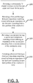
- FIG. 3 illustrates a block diagram associated with a method of manufacturing or otherwise providing a circulator in accordance with an example embodiment. As shown in FIG. 3 , the method may include providing a substantially Y-shaped conductive strip between upper and lower ferrite pucks at operation 200.
- the method may further include providing a first port having a first port impedance matching circuit defining an impedance of the first port extending from a first portion of the conductive strip at operation 210, providing a second port having a second port impedance matching circuit defining an impedance of the second port extending from a second portion of the conductive strip at operation 220, and providing a third port having a third port impedance matching circuit defining an impedance of the third port extending from a third portion of the conductive strip at operation 230.
- the impedance of the first port may be provided to match an impedance of a first external circuit
- the impedance of the second port may be provided to match an impedance of a second external circuit
- the impedance of the third port may be provided to match an impedance of a third external circuit.
- the impedance of the third port may be provided to be different than the impedance of the first port.
- the impedance of the third port may be provided to be different than the impedance of the first port by altering one or both of dielectric materials used and dimensions of conductive materials used to define the first port impedance matching circuit and the third port impedance matching circuit.
Landscapes
- Amplifiers (AREA)
- Non-Reversible Transmitting Devices (AREA)
Claims (8)
- Zirkulator (10, 100), der folgendes umfasst:einen ersten Port (30, 150) mit einer Impedanzanpassungsschaltung (40) des ersten Ports, die eine Impedanz des ersten Ports (30, 150) definiert;einen zweiten Port (32, 152) mit einer Impedanzanpassungsschaltung (42) des zweiten Ports, die eine Impedanz des zweiten Ports (32, 152) definiert; undeinen dritten Port (34, 154) mit einer Impedanzanpassungsschaltung (44) des dritten Ports, die eine Impedanz des dritten Ports (34, 154) definiert,wobei die Impedanz des ersten Ports (30, 150) so ausgelegt ist, dass sie an eine Impedanz einer ersten externen Schaltung (50) angepasst ist, die Impedanz des zweiten Ports (32, 152) so ausgelegt ist, dass sie an eine Impedanz einer zweiten externen Schaltung (52) angepasst ist, und die Impedanz des dritten Ports (34, 154) so ausgelegt ist, dass sie an eine Impedanz einer dritten externen Schaltung (54) angepasst ist,wobei die Impedanz des dritten Ports (34, 154) sich von der Impedanz des ersten Ports (30, 150) unterscheidet,wobei die Impedanzanpassungsschaltung (40) des ersten Ports ein erstes oberes dielektrisches Material (140) und ein erstes unteres dielektrisches Material (141) umfasst, die auf gegenüberliegenden Seiten eines ersten Transformators (130) angeordnet sind, wobei die Impedanzanpassungsschaltung (42) des zweiten Ports ein zweites oberes dielektrisches Material (144) und ein zweites unteres dielektrisches Material (145) umfasst, die auf gegenüberliegenden Seiten eines zweiten Transformators (132) angeordnet sind, undwobei die Impedanzanpassungsschaltung (44) des dritten Ports ein drittes oberes dielektrisches Material (148) und ein drittes unteres dielektrisches Material (149) umfasst, die auf gegenüberliegenden Seiten eines dritten Transformators (134) angeordnet sind, wobei das erste obere dielektrische Material (140) sich von dem dritten oberen dielektrischen Material (148) unterscheidet,wobei sich das erste untere dielektrische Material (141) von dem dritten unteren dielektrischen Material (149) unterscheidet, undwobei die Abmessungen des ersten, zweiten und dritten Transformators (130, 132, 134) im wesentlichen gleich sind.
- Zirkulator (10, 100) nach Anspruch 1, wobei die Impedanz des ersten Ports (30, 150) im wesentlichen die gleiche ist wie die Impedanz des zweiten Ports (32, 152).
- Zirkulator (10, 100) nach Anspruch 1, wobei sich die Impedanz des dritten Ports (34, 154) von der Impedanz des ersten Ports (30, 150) um mindestens 20% der Impedanz des dritten Ports (34, 154) unterscheidet.
- Zirkulator (10, 100) nach Anspruch 1, wobei die Impedanz des ersten Ports (30, 150) etwa 50 Ohm und die Impedanz des dritten Ports (34, 154) weniger als 50 Ohm beträgt.
- Leistungsverstärker mit mindestens einem Zirkulator (10, 100) nach Anspruch 1.
- Leistungsverstärker nach Anspruch 5, wobei die Impedanz des ersten Ports (30, 150) im wesentlichen die gleiche ist wie die Impedanz des zweiten Ports (32, 152).
- Leistungsverstärker nach Anspruch 5, wobei sich die Impedanz des dritten Ports (34, 154) von der Impedanz des ersten Ports (30, 150) um mindestens 20% der Impedanz des dritten Ports (34, 154) unterscheidet.
- Leistungsverstärker nach Anspruch 5, wobei die Impedanz des ersten Ports (30, 150) etwa 50 Ohm und die Impedanz des dritten Ports (34, 154) weniger als 50 Ohm beträgt.
Applications Claiming Priority (2)
| Application Number | Priority Date | Filing Date | Title |
|---|---|---|---|
| US14/051,011 US9246202B1 (en) | 2013-10-10 | 2013-10-10 | Low impedance circulator |
| PCT/US2014/058798 WO2015054022A1 (en) | 2013-10-10 | 2014-10-02 | Low impedance circulator |
Publications (2)
| Publication Number | Publication Date |
|---|---|
| EP3055901A1 EP3055901A1 (de) | 2016-08-17 |
| EP3055901B1 true EP3055901B1 (de) | 2020-04-29 |
Family
ID=51844834
Family Applications (1)
| Application Number | Title | Priority Date | Filing Date |
|---|---|---|---|
| EP14792642.2A Active EP3055901B1 (de) | 2013-10-10 | 2014-10-02 | Niederohmiger zirkulator |
Country Status (6)
| Country | Link |
|---|---|
| US (1) | US9246202B1 (de) |
| EP (1) | EP3055901B1 (de) |
| JP (1) | JP6494642B2 (de) |
| AU (1) | AU2014332362A1 (de) |
| CA (1) | CA2926939C (de) |
| WO (1) | WO2015054022A1 (de) |
Families Citing this family (4)
| Publication number | Priority date | Publication date | Assignee | Title |
|---|---|---|---|---|
| JPWO2016047323A1 (ja) * | 2014-09-25 | 2017-06-15 | 株式会社村田製作所 | フロントエンド回路および通信装置 |
| US11112489B2 (en) | 2018-12-28 | 2021-09-07 | Intel Corporation | Radar systems and methods having isolator driven mixer |
| EP4367746A4 (de) * | 2021-07-08 | 2025-03-05 | Telefonaktiebolaget LM Ericsson (publ) | Verbesserte topologie für ein elektrisches filter |
| CN121172418A (zh) * | 2024-06-18 | 2025-12-19 | 华为技术有限公司 | 非可逆器件、射频模组以及通信装置 |
Family Cites Families (6)
| Publication number | Priority date | Publication date | Assignee | Title |
|---|---|---|---|---|
| JPS5247393Y2 (de) * | 1972-03-28 | 1977-10-27 | ||
| JPS5419803Y2 (de) * | 1973-05-19 | 1979-07-20 | ||
| CN1319277A (zh) | 1999-07-29 | 2001-10-24 | Tdk株式会社 | 具有内置功率放大器的隔离装置 |
| US7242264B1 (en) * | 2005-04-21 | 2007-07-10 | Hoton How | Method and apparatus of obtaining broadband circulator/isolator operation by shaping the bias magnetic field |
| JP4817050B2 (ja) | 2006-02-07 | 2011-11-16 | 日立金属株式会社 | 非可逆回路素子 |
| US8138848B2 (en) | 2008-11-03 | 2012-03-20 | Anaren, Inc. | Circulator/isolator with an asymmetric resonator |
-
2013
- 2013-10-10 US US14/051,011 patent/US9246202B1/en active Active
-
2014
- 2014-10-02 AU AU2014332362A patent/AU2014332362A1/en not_active Abandoned
- 2014-10-02 EP EP14792642.2A patent/EP3055901B1/de active Active
- 2014-10-02 JP JP2016547838A patent/JP6494642B2/ja active Active
- 2014-10-02 WO PCT/US2014/058798 patent/WO2015054022A1/en not_active Ceased
- 2014-10-02 CA CA2926939A patent/CA2926939C/en active Active
Non-Patent Citations (1)
| Title |
|---|
| None * |
Also Published As
| Publication number | Publication date |
|---|---|
| CA2926939A1 (en) | 2015-04-16 |
| US9246202B1 (en) | 2016-01-26 |
| EP3055901A1 (de) | 2016-08-17 |
| CA2926939C (en) | 2018-08-14 |
| JP6494642B2 (ja) | 2019-04-03 |
| WO2015054022A1 (en) | 2015-04-16 |
| AU2014332362A1 (en) | 2016-04-28 |
| JP2016533141A (ja) | 2016-10-20 |
Similar Documents
| Publication | Publication Date | Title |
|---|---|---|
| Zhu et al. | Design of wideband in-phase and out-of-phase power dividers using microstrip-to-slotline transitions and slotline resonators | |
| Chiu et al. | A parallel-strip ring power divider with high isolation and arbitrary power-dividing ratio | |
| US9093734B2 (en) | Miniature radio frequency directional coupler for cellular applications | |
| EP3444892B1 (de) | Leistungsteiler/-kombinierer | |
| Abbosh | Planar out-of-phase power divider/combiner for wideband high power microwave applications | |
| US10535912B2 (en) | Wideband gysel power divider | |
| Moradi et al. | Gysel power divider with efficient second and third harmonic suppression using one resistor | |
| Amini et al. | A single-layer balanced directional coupler design based on crossover structures | |
| CA2926939C (en) | Low impedance circulator | |
| Lyu et al. | A new design of filtering power dividers with arbitrary constant phase difference, impedance transformation, and good isolation | |
| Wu et al. | A planar microstrip crossover with lumped inductors for three intersecting channels | |
| KR101464930B1 (ko) | 광대역 특성을 갖는 소형 브랜치라인 커플러 | |
| CN111525222B (zh) | 基于交叉型慢波传输线的小型化共面波导等分功分器 | |
| KR20190096041A (ko) | 광대역 대전력 결합기 | |
| Piacibello et al. | Generalized symmetrical 3 dB power dividers with complex termination impedances | |
| Wu et al. | Generalized high‐isolation n‐way Gysel power divider with arbitrary power ratio and different real terminated impedances | |
| US5796317A (en) | Variable impedance transmission line and high-power broadband reduced-size power divider/combiner employing same | |
| Bharti et al. | SIW based in-phase Gysel equal power divider for X-band application | |
| Abouelnaga et al. | Reconfigurable 3/6 dB Novel branch line coupler | |
| Moghaddam et al. | 180 hybrid using a novel planar balun on suspended substrate for beam forming network applications | |
| US7746193B2 (en) | Miniature 180 degree hybrid coupler | |
| US9966646B1 (en) | Coupler with lumped components | |
| Huang et al. | Design of Ka-band high-performance circulator | |
| Kim et al. | Wideband bandpass filtering branch‐line balun with high‐isolation | |
| Hu et al. | Compact multi-layer N-way power divider with closed-ring-shaped isolation network |
Legal Events
| Date | Code | Title | Description |
|---|---|---|---|
| PUAI | Public reference made under article 153(3) epc to a published international application that has entered the european phase |
Free format text: ORIGINAL CODE: 0009012 |
|
| 17P | Request for examination filed |
Effective date: 20160419 |
|
| AK | Designated contracting states |
Kind code of ref document: A1 Designated state(s): AL AT BE BG CH CY CZ DE DK EE ES FI FR GB GR HR HU IE IS IT LI LT LU LV MC MK MT NL NO PL PT RO RS SE SI SK SM TR |
|
| AX | Request for extension of the european patent |
Extension state: BA ME |
|
| DAX | Request for extension of the european patent (deleted) | ||
| STAA | Information on the status of an ep patent application or granted ep patent |
Free format text: STATUS: EXAMINATION IS IN PROGRESS |
|
| 17Q | First examination report despatched |
Effective date: 20190214 |
|
| GRAP | Despatch of communication of intention to grant a patent |
Free format text: ORIGINAL CODE: EPIDOSNIGR1 |
|
| STAA | Information on the status of an ep patent application or granted ep patent |
Free format text: STATUS: GRANT OF PATENT IS INTENDED |
|
| INTG | Intention to grant announced |
Effective date: 20191204 |
|
| GRAS | Grant fee paid |
Free format text: ORIGINAL CODE: EPIDOSNIGR3 |
|
| GRAA | (expected) grant |
Free format text: ORIGINAL CODE: 0009210 |
|
| STAA | Information on the status of an ep patent application or granted ep patent |
Free format text: STATUS: THE PATENT HAS BEEN GRANTED |
|
| AK | Designated contracting states |
Kind code of ref document: B1 Designated state(s): AL AT BE BG CH CY CZ DE DK EE ES FI FR GB GR HR HU IE IS IT LI LT LU LV MC MK MT NL NO PL PT RO RS SE SI SK SM TR |
|
| REG | Reference to a national code |
Ref country code: GB Ref legal event code: FG4D |
|
| REG | Reference to a national code |
Ref country code: CH Ref legal event code: EP |
|
| REG | Reference to a national code |
Ref country code: AT Ref legal event code: REF Ref document number: 1264680 Country of ref document: AT Kind code of ref document: T Effective date: 20200515 |
|
| REG | Reference to a national code |
Ref country code: DE Ref legal event code: R096 Ref document number: 602014064592 Country of ref document: DE |
|
| REG | Reference to a national code |
Ref country code: IE Ref legal event code: FG4D |
|
| REG | Reference to a national code |
Ref country code: NL Ref legal event code: MP Effective date: 20200429 |
|
| REG | Reference to a national code |
Ref country code: LT Ref legal event code: MG4D |
|
| PG25 | Lapsed in a contracting state [announced via postgrant information from national office to epo] |
Ref country code: LT Free format text: LAPSE BECAUSE OF FAILURE TO SUBMIT A TRANSLATION OF THE DESCRIPTION OR TO PAY THE FEE WITHIN THE PRESCRIBED TIME-LIMIT Effective date: 20200429 Ref country code: NO Free format text: LAPSE BECAUSE OF FAILURE TO SUBMIT A TRANSLATION OF THE DESCRIPTION OR TO PAY THE FEE WITHIN THE PRESCRIBED TIME-LIMIT Effective date: 20200729 Ref country code: SE Free format text: LAPSE BECAUSE OF FAILURE TO SUBMIT A TRANSLATION OF THE DESCRIPTION OR TO PAY THE FEE WITHIN THE PRESCRIBED TIME-LIMIT Effective date: 20200429 Ref country code: IS Free format text: LAPSE BECAUSE OF FAILURE TO SUBMIT A TRANSLATION OF THE DESCRIPTION OR TO PAY THE FEE WITHIN THE PRESCRIBED TIME-LIMIT Effective date: 20200829 Ref country code: FI Free format text: LAPSE BECAUSE OF FAILURE TO SUBMIT A TRANSLATION OF THE DESCRIPTION OR TO PAY THE FEE WITHIN THE PRESCRIBED TIME-LIMIT Effective date: 20200429 Ref country code: GR Free format text: LAPSE BECAUSE OF FAILURE TO SUBMIT A TRANSLATION OF THE DESCRIPTION OR TO PAY THE FEE WITHIN THE PRESCRIBED TIME-LIMIT Effective date: 20200730 Ref country code: PT Free format text: LAPSE BECAUSE OF FAILURE TO SUBMIT A TRANSLATION OF THE DESCRIPTION OR TO PAY THE FEE WITHIN THE PRESCRIBED TIME-LIMIT Effective date: 20200831 |
|
| REG | Reference to a national code |
Ref country code: AT Ref legal event code: MK05 Ref document number: 1264680 Country of ref document: AT Kind code of ref document: T Effective date: 20200429 |
|
| PG25 | Lapsed in a contracting state [announced via postgrant information from national office to epo] |
Ref country code: RS Free format text: LAPSE BECAUSE OF FAILURE TO SUBMIT A TRANSLATION OF THE DESCRIPTION OR TO PAY THE FEE WITHIN THE PRESCRIBED TIME-LIMIT Effective date: 20200429 Ref country code: HR Free format text: LAPSE BECAUSE OF FAILURE TO SUBMIT A TRANSLATION OF THE DESCRIPTION OR TO PAY THE FEE WITHIN THE PRESCRIBED TIME-LIMIT Effective date: 20200429 Ref country code: BG Free format text: LAPSE BECAUSE OF FAILURE TO SUBMIT A TRANSLATION OF THE DESCRIPTION OR TO PAY THE FEE WITHIN THE PRESCRIBED TIME-LIMIT Effective date: 20200729 Ref country code: LV Free format text: LAPSE BECAUSE OF FAILURE TO SUBMIT A TRANSLATION OF THE DESCRIPTION OR TO PAY THE FEE WITHIN THE PRESCRIBED TIME-LIMIT Effective date: 20200429 |
|
| PG25 | Lapsed in a contracting state [announced via postgrant information from national office to epo] |
Ref country code: NL Free format text: LAPSE BECAUSE OF FAILURE TO SUBMIT A TRANSLATION OF THE DESCRIPTION OR TO PAY THE FEE WITHIN THE PRESCRIBED TIME-LIMIT Effective date: 20200429 Ref country code: AL Free format text: LAPSE BECAUSE OF FAILURE TO SUBMIT A TRANSLATION OF THE DESCRIPTION OR TO PAY THE FEE WITHIN THE PRESCRIBED TIME-LIMIT Effective date: 20200429 |
|
| PG25 | Lapsed in a contracting state [announced via postgrant information from national office to epo] |
Ref country code: IT Free format text: LAPSE BECAUSE OF FAILURE TO SUBMIT A TRANSLATION OF THE DESCRIPTION OR TO PAY THE FEE WITHIN THE PRESCRIBED TIME-LIMIT Effective date: 20200429 Ref country code: AT Free format text: LAPSE BECAUSE OF FAILURE TO SUBMIT A TRANSLATION OF THE DESCRIPTION OR TO PAY THE FEE WITHIN THE PRESCRIBED TIME-LIMIT Effective date: 20200429 Ref country code: DK Free format text: LAPSE BECAUSE OF FAILURE TO SUBMIT A TRANSLATION OF THE DESCRIPTION OR TO PAY THE FEE WITHIN THE PRESCRIBED TIME-LIMIT Effective date: 20200429 Ref country code: SM Free format text: LAPSE BECAUSE OF FAILURE TO SUBMIT A TRANSLATION OF THE DESCRIPTION OR TO PAY THE FEE WITHIN THE PRESCRIBED TIME-LIMIT Effective date: 20200429 Ref country code: EE Free format text: LAPSE BECAUSE OF FAILURE TO SUBMIT A TRANSLATION OF THE DESCRIPTION OR TO PAY THE FEE WITHIN THE PRESCRIBED TIME-LIMIT Effective date: 20200429 Ref country code: RO Free format text: LAPSE BECAUSE OF FAILURE TO SUBMIT A TRANSLATION OF THE DESCRIPTION OR TO PAY THE FEE WITHIN THE PRESCRIBED TIME-LIMIT Effective date: 20200429 Ref country code: ES Free format text: LAPSE BECAUSE OF FAILURE TO SUBMIT A TRANSLATION OF THE DESCRIPTION OR TO PAY THE FEE WITHIN THE PRESCRIBED TIME-LIMIT Effective date: 20200429 Ref country code: CZ Free format text: LAPSE BECAUSE OF FAILURE TO SUBMIT A TRANSLATION OF THE DESCRIPTION OR TO PAY THE FEE WITHIN THE PRESCRIBED TIME-LIMIT Effective date: 20200429 |
|
| REG | Reference to a national code |
Ref country code: DE Ref legal event code: R097 Ref document number: 602014064592 Country of ref document: DE |
|
| PG25 | Lapsed in a contracting state [announced via postgrant information from national office to epo] |
Ref country code: SK Free format text: LAPSE BECAUSE OF FAILURE TO SUBMIT A TRANSLATION OF THE DESCRIPTION OR TO PAY THE FEE WITHIN THE PRESCRIBED TIME-LIMIT Effective date: 20200429 Ref country code: PL Free format text: LAPSE BECAUSE OF FAILURE TO SUBMIT A TRANSLATION OF THE DESCRIPTION OR TO PAY THE FEE WITHIN THE PRESCRIBED TIME-LIMIT Effective date: 20200429 |
|
| PLBE | No opposition filed within time limit |
Free format text: ORIGINAL CODE: 0009261 |
|
| STAA | Information on the status of an ep patent application or granted ep patent |
Free format text: STATUS: NO OPPOSITION FILED WITHIN TIME LIMIT |
|
| 26N | No opposition filed |
Effective date: 20210201 |
|
| PG25 | Lapsed in a contracting state [announced via postgrant information from national office to epo] |
Ref country code: SI Free format text: LAPSE BECAUSE OF FAILURE TO SUBMIT A TRANSLATION OF THE DESCRIPTION OR TO PAY THE FEE WITHIN THE PRESCRIBED TIME-LIMIT Effective date: 20200429 |
|
| REG | Reference to a national code |
Ref country code: CH Ref legal event code: PL |
|
| PG25 | Lapsed in a contracting state [announced via postgrant information from national office to epo] |
Ref country code: MC Free format text: LAPSE BECAUSE OF FAILURE TO SUBMIT A TRANSLATION OF THE DESCRIPTION OR TO PAY THE FEE WITHIN THE PRESCRIBED TIME-LIMIT Effective date: 20200429 Ref country code: LU Free format text: LAPSE BECAUSE OF NON-PAYMENT OF DUE FEES Effective date: 20201002 |
|
| REG | Reference to a national code |
Ref country code: BE Ref legal event code: MM Effective date: 20201031 |
|
| PG25 | Lapsed in a contracting state [announced via postgrant information from national office to epo] |
Ref country code: CH Free format text: LAPSE BECAUSE OF NON-PAYMENT OF DUE FEES Effective date: 20201031 Ref country code: BE Free format text: LAPSE BECAUSE OF NON-PAYMENT OF DUE FEES Effective date: 20201031 Ref country code: LI Free format text: LAPSE BECAUSE OF NON-PAYMENT OF DUE FEES Effective date: 20201031 |
|
| PG25 | Lapsed in a contracting state [announced via postgrant information from national office to epo] |
Ref country code: IE Free format text: LAPSE BECAUSE OF NON-PAYMENT OF DUE FEES Effective date: 20201002 |
|
| PG25 | Lapsed in a contracting state [announced via postgrant information from national office to epo] |
Ref country code: TR Free format text: LAPSE BECAUSE OF FAILURE TO SUBMIT A TRANSLATION OF THE DESCRIPTION OR TO PAY THE FEE WITHIN THE PRESCRIBED TIME-LIMIT Effective date: 20200429 Ref country code: MT Free format text: LAPSE BECAUSE OF FAILURE TO SUBMIT A TRANSLATION OF THE DESCRIPTION OR TO PAY THE FEE WITHIN THE PRESCRIBED TIME-LIMIT Effective date: 20200429 Ref country code: CY Free format text: LAPSE BECAUSE OF FAILURE TO SUBMIT A TRANSLATION OF THE DESCRIPTION OR TO PAY THE FEE WITHIN THE PRESCRIBED TIME-LIMIT Effective date: 20200429 |
|
| PG25 | Lapsed in a contracting state [announced via postgrant information from national office to epo] |
Ref country code: MK Free format text: LAPSE BECAUSE OF FAILURE TO SUBMIT A TRANSLATION OF THE DESCRIPTION OR TO PAY THE FEE WITHIN THE PRESCRIBED TIME-LIMIT Effective date: 20200429 |
|
| P01 | Opt-out of the competence of the unified patent court (upc) registered |
Effective date: 20230508 |
|
| PGFP | Annual fee paid to national office [announced via postgrant information from national office to epo] |
Ref country code: DE Payment date: 20251021 Year of fee payment: 12 |
|
| PGFP | Annual fee paid to national office [announced via postgrant information from national office to epo] |
Ref country code: GB Payment date: 20251022 Year of fee payment: 12 |
|
| PGFP | Annual fee paid to national office [announced via postgrant information from national office to epo] |
Ref country code: FR Payment date: 20251030 Year of fee payment: 12 |