EP3054037A1 - METHOD FOR GROWING -Ga2O3-BASED SINGLE CRYSTAL FILM, AND CRYSTALLINE LAYERED STRUCTURE - Google Patents
METHOD FOR GROWING -Ga2O3-BASED SINGLE CRYSTAL FILM, AND CRYSTALLINE LAYERED STRUCTURE Download PDFInfo
- Publication number
- EP3054037A1 EP3054037A1 EP14849461.0A EP14849461A EP3054037A1 EP 3054037 A1 EP3054037 A1 EP 3054037A1 EP 14849461 A EP14849461 A EP 14849461A EP 3054037 A1 EP3054037 A1 EP 3054037A1
- Authority
- EP
- European Patent Office
- Prior art keywords
- crystal film
- gas
- single crystal
- growing
- based single
- Prior art date
- Legal status (The legal status is an assumption and is not a legal conclusion. Google has not performed a legal analysis and makes no representation as to the accuracy of the status listed.)
- Granted
Links
Images




Classifications
-
- C—CHEMISTRY; METALLURGY
- C30—CRYSTAL GROWTH
- C30B—SINGLE-CRYSTAL GROWTH; UNIDIRECTIONAL SOLIDIFICATION OF EUTECTIC MATERIAL OR UNIDIRECTIONAL DEMIXING OF EUTECTOID MATERIAL; REFINING BY ZONE-MELTING OF MATERIAL; PRODUCTION OF A HOMOGENEOUS POLYCRYSTALLINE MATERIAL WITH DEFINED STRUCTURE; SINGLE CRYSTALS OR HOMOGENEOUS POLYCRYSTALLINE MATERIAL WITH DEFINED STRUCTURE; AFTER-TREATMENT OF SINGLE CRYSTALS OR A HOMOGENEOUS POLYCRYSTALLINE MATERIAL WITH DEFINED STRUCTURE; APPARATUS THEREFOR
- C30B25/00—Single-crystal growth by chemical reaction of reactive gases, e.g. chemical vapour-deposition growth
- C30B25/02—Epitaxial-layer growth
- C30B25/16—Controlling or regulating
- C30B25/165—Controlling or regulating the flow of the reactive gases
-
- C—CHEMISTRY; METALLURGY
- C23—COATING METALLIC MATERIAL; COATING MATERIAL WITH METALLIC MATERIAL; CHEMICAL SURFACE TREATMENT; DIFFUSION TREATMENT OF METALLIC MATERIAL; COATING BY VACUUM EVAPORATION, BY SPUTTERING, BY ION IMPLANTATION OR BY CHEMICAL VAPOUR DEPOSITION, IN GENERAL; INHIBITING CORROSION OF METALLIC MATERIAL OR INCRUSTATION IN GENERAL
- C23C—COATING METALLIC MATERIAL; COATING MATERIAL WITH METALLIC MATERIAL; SURFACE TREATMENT OF METALLIC MATERIAL BY DIFFUSION INTO THE SURFACE, BY CHEMICAL CONVERSION OR SUBSTITUTION; COATING BY VACUUM EVAPORATION, BY SPUTTERING, BY ION IMPLANTATION OR BY CHEMICAL VAPOUR DEPOSITION, IN GENERAL
- C23C16/00—Chemical coating by decomposition of gaseous compounds, without leaving reaction products of surface material in the coating, i.e. chemical vapour deposition [CVD] processes
- C23C16/22—Chemical coating by decomposition of gaseous compounds, without leaving reaction products of surface material in the coating, i.e. chemical vapour deposition [CVD] processes characterised by the deposition of inorganic material, other than metallic material
- C23C16/30—Deposition of compounds, mixtures or solid solutions, e.g. borides, carbides, nitrides
- C23C16/40—Oxides
-
- C—CHEMISTRY; METALLURGY
- C23—COATING METALLIC MATERIAL; COATING MATERIAL WITH METALLIC MATERIAL; CHEMICAL SURFACE TREATMENT; DIFFUSION TREATMENT OF METALLIC MATERIAL; COATING BY VACUUM EVAPORATION, BY SPUTTERING, BY ION IMPLANTATION OR BY CHEMICAL VAPOUR DEPOSITION, IN GENERAL; INHIBITING CORROSION OF METALLIC MATERIAL OR INCRUSTATION IN GENERAL
- C23C—COATING METALLIC MATERIAL; COATING MATERIAL WITH METALLIC MATERIAL; SURFACE TREATMENT OF METALLIC MATERIAL BY DIFFUSION INTO THE SURFACE, BY CHEMICAL CONVERSION OR SUBSTITUTION; COATING BY VACUUM EVAPORATION, BY SPUTTERING, BY ION IMPLANTATION OR BY CHEMICAL VAPOUR DEPOSITION, IN GENERAL
- C23C16/00—Chemical coating by decomposition of gaseous compounds, without leaving reaction products of surface material in the coating, i.e. chemical vapour deposition [CVD] processes
- C23C16/44—Chemical coating by decomposition of gaseous compounds, without leaving reaction products of surface material in the coating, i.e. chemical vapour deposition [CVD] processes characterised by the method of coating
- C23C16/448—Chemical coating by decomposition of gaseous compounds, without leaving reaction products of surface material in the coating, i.e. chemical vapour deposition [CVD] processes characterised by the method of coating characterised by the method used for generating reactive gas streams, e.g. by evaporation or sublimation of precursor materials
- C23C16/4488—Chemical coating by decomposition of gaseous compounds, without leaving reaction products of surface material in the coating, i.e. chemical vapour deposition [CVD] processes characterised by the method of coating characterised by the method used for generating reactive gas streams, e.g. by evaporation or sublimation of precursor materials by in situ generation of reactive gas by chemical or electrochemical reaction
-
- C—CHEMISTRY; METALLURGY
- C30—CRYSTAL GROWTH
- C30B—SINGLE-CRYSTAL GROWTH; UNIDIRECTIONAL SOLIDIFICATION OF EUTECTIC MATERIAL OR UNIDIRECTIONAL DEMIXING OF EUTECTOID MATERIAL; REFINING BY ZONE-MELTING OF MATERIAL; PRODUCTION OF A HOMOGENEOUS POLYCRYSTALLINE MATERIAL WITH DEFINED STRUCTURE; SINGLE CRYSTALS OR HOMOGENEOUS POLYCRYSTALLINE MATERIAL WITH DEFINED STRUCTURE; AFTER-TREATMENT OF SINGLE CRYSTALS OR A HOMOGENEOUS POLYCRYSTALLINE MATERIAL WITH DEFINED STRUCTURE; APPARATUS THEREFOR
- C30B25/00—Single-crystal growth by chemical reaction of reactive gases, e.g. chemical vapour-deposition growth
- C30B25/02—Epitaxial-layer growth
-
- C—CHEMISTRY; METALLURGY
- C30—CRYSTAL GROWTH
- C30B—SINGLE-CRYSTAL GROWTH; UNIDIRECTIONAL SOLIDIFICATION OF EUTECTIC MATERIAL OR UNIDIRECTIONAL DEMIXING OF EUTECTOID MATERIAL; REFINING BY ZONE-MELTING OF MATERIAL; PRODUCTION OF A HOMOGENEOUS POLYCRYSTALLINE MATERIAL WITH DEFINED STRUCTURE; SINGLE CRYSTALS OR HOMOGENEOUS POLYCRYSTALLINE MATERIAL WITH DEFINED STRUCTURE; AFTER-TREATMENT OF SINGLE CRYSTALS OR A HOMOGENEOUS POLYCRYSTALLINE MATERIAL WITH DEFINED STRUCTURE; APPARATUS THEREFOR
- C30B29/00—Single crystals or homogeneous polycrystalline material with defined structure characterised by the material or by their shape
- C30B29/10—Inorganic compounds or compositions
- C30B29/16—Oxides
-
- H—ELECTRICITY
- H10—SEMICONDUCTOR DEVICES; ELECTRIC SOLID-STATE DEVICES NOT OTHERWISE PROVIDED FOR
- H10D—INORGANIC ELECTRIC SEMICONDUCTOR DEVICES
- H10D62/00—Semiconductor bodies, or regions thereof, of devices having potential barriers
- H10D62/40—Crystalline structures
-
- H—ELECTRICITY
- H10—SEMICONDUCTOR DEVICES; ELECTRIC SOLID-STATE DEVICES NOT OTHERWISE PROVIDED FOR
- H10D—INORGANIC ELECTRIC SEMICONDUCTOR DEVICES
- H10D62/00—Semiconductor bodies, or regions thereof, of devices having potential barriers
- H10D62/80—Semiconductor bodies, or regions thereof, of devices having potential barriers characterised by the materials
-
- H—ELECTRICITY
- H10—SEMICONDUCTOR DEVICES; ELECTRIC SOLID-STATE DEVICES NOT OTHERWISE PROVIDED FOR
- H10P—GENERIC PROCESSES OR APPARATUS FOR THE MANUFACTURE OR TREATMENT OF DEVICES COVERED BY CLASS H10
- H10P14/00—Formation of materials, e.g. in the shape of layers or pillars
- H10P14/20—Formation of materials, e.g. in the shape of layers or pillars of semiconductor materials
-
- H—ELECTRICITY
- H10—SEMICONDUCTOR DEVICES; ELECTRIC SOLID-STATE DEVICES NOT OTHERWISE PROVIDED FOR
- H10P—GENERIC PROCESSES OR APPARATUS FOR THE MANUFACTURE OR TREATMENT OF DEVICES COVERED BY CLASS H10
- H10P14/00—Formation of materials, e.g. in the shape of layers or pillars
- H10P14/20—Formation of materials, e.g. in the shape of layers or pillars of semiconductor materials
- H10P14/24—Formation of materials, e.g. in the shape of layers or pillars of semiconductor materials using chemical vapour deposition [CVD]
-
- H—ELECTRICITY
- H10—SEMICONDUCTOR DEVICES; ELECTRIC SOLID-STATE DEVICES NOT OTHERWISE PROVIDED FOR
- H10P—GENERIC PROCESSES OR APPARATUS FOR THE MANUFACTURE OR TREATMENT OF DEVICES COVERED BY CLASS H10
- H10P14/00—Formation of materials, e.g. in the shape of layers or pillars
- H10P14/20—Formation of materials, e.g. in the shape of layers or pillars of semiconductor materials
- H10P14/29—Formation of materials, e.g. in the shape of layers or pillars of semiconductor materials characterised by the substrates
- H10P14/2901—Materials
- H10P14/2918—Materials being semiconductor metal oxides
-
- H—ELECTRICITY
- H10—SEMICONDUCTOR DEVICES; ELECTRIC SOLID-STATE DEVICES NOT OTHERWISE PROVIDED FOR
- H10P—GENERIC PROCESSES OR APPARATUS FOR THE MANUFACTURE OR TREATMENT OF DEVICES COVERED BY CLASS H10
- H10P14/00—Formation of materials, e.g. in the shape of layers or pillars
- H10P14/20—Formation of materials, e.g. in the shape of layers or pillars of semiconductor materials
- H10P14/29—Formation of materials, e.g. in the shape of layers or pillars of semiconductor materials characterised by the substrates
- H10P14/2926—Crystal orientations
-
- H—ELECTRICITY
- H10—SEMICONDUCTOR DEVICES; ELECTRIC SOLID-STATE DEVICES NOT OTHERWISE PROVIDED FOR
- H10P—GENERIC PROCESSES OR APPARATUS FOR THE MANUFACTURE OR TREATMENT OF DEVICES COVERED BY CLASS H10
- H10P14/00—Formation of materials, e.g. in the shape of layers or pillars
- H10P14/20—Formation of materials, e.g. in the shape of layers or pillars of semiconductor materials
- H10P14/34—Deposited materials, e.g. layers
- H10P14/3402—Deposited materials, e.g. layers characterised by the chemical composition
- H10P14/3434—Deposited materials, e.g. layers characterised by the chemical composition being oxide semiconductor materials
-
- H—ELECTRICITY
- H10—SEMICONDUCTOR DEVICES; ELECTRIC SOLID-STATE DEVICES NOT OTHERWISE PROVIDED FOR
- H10P—GENERIC PROCESSES OR APPARATUS FOR THE MANUFACTURE OR TREATMENT OF DEVICES COVERED BY CLASS H10
- H10P14/00—Formation of materials, e.g. in the shape of layers or pillars
- H10P14/20—Formation of materials, e.g. in the shape of layers or pillars of semiconductor materials
- H10P14/34—Deposited materials, e.g. layers
- H10P14/3438—Doping during depositing
- H10P14/3441—Conductivity type
- H10P14/3442—N-type
-
- H—ELECTRICITY
- H10—SEMICONDUCTOR DEVICES; ELECTRIC SOLID-STATE DEVICES NOT OTHERWISE PROVIDED FOR
- H10P—GENERIC PROCESSES OR APPARATUS FOR THE MANUFACTURE OR TREATMENT OF DEVICES COVERED BY CLASS H10
- H10P14/00—Formation of materials, e.g. in the shape of layers or pillars
- H10P14/20—Formation of materials, e.g. in the shape of layers or pillars of semiconductor materials
- H10P14/34—Deposited materials, e.g. layers
- H10P14/3451—Structure
- H10P14/3452—Microstructure
-
- H—ELECTRICITY
- H10—SEMICONDUCTOR DEVICES; ELECTRIC SOLID-STATE DEVICES NOT OTHERWISE PROVIDED FOR
- H10P—GENERIC PROCESSES OR APPARATUS FOR THE MANUFACTURE OR TREATMENT OF DEVICES COVERED BY CLASS H10
- H10P14/00—Formation of materials, e.g. in the shape of layers or pillars
- H10P14/20—Formation of materials, e.g. in the shape of layers or pillars of semiconductor materials
- H10P14/34—Deposited materials, e.g. layers
- H10P14/3451—Structure
- H10P14/3452—Microstructure
- H10P14/3458—Monocrystalline
Definitions
- the invention relates to a method for growing a ⁇ -Ga 2 O 3 -based single crystal film and a crystalline layered structure.
- the MBE (Molecular Beam Epitaxy) method and the PLD (Pulsed Laser Deposition) method are known as a growth method of ⁇ -Ga 2 O 3 single crystal film (see, e.g., PTL 1 and PTL 2).
- Other growth methods thereof, the sol-gel process, the MOCVD (Metal Organic Chemical Vapor Deposition) process and the mist CVD process are also known.
- the MBE method is conducted, however, such that crystal is grown in a high vacuum chamber.
- it is difficult to increase the diameter of a ⁇ -Ga 2 O 3 single crystal film.
- a high-quality film can be generally obtained by increasing the growth temperature, a sufficient film growth rate is not obtained due to an increase in re-evaporation of source gases and it is thus not suitable for mass production.
- the PLD method is not suitable for growing a film with a large area since a source (a raw material supply source to a substrate) is a point source which causes a growth rate to be different between a portion immediately above the source and other portions and in-plane distribution of film thickness is likely to be non-uniform. In addition, it takes long time to form a thick film due to a low film growth rate, hence, not suitable for mass production.
- the MOCVD method and the mist CVD method it is relatively easy to increase a diameter but it is difficult to obtain single crystal films with high purity since impurities contained in the used materials are incorporated into the ⁇ -Ga 2 O 3 single crystal film during epitaxial growth.
- a growth method of a ⁇ -Ga 2 O 3 -based single crystal film defined by [1] to [8] below will be provided.
- a method for growing a ⁇ -Ga 2 O 3 -based single crystal film can be provided that allows a high-quality and large-diameter ⁇ -Ga 2 O 3 -based single crystal film to grow efficiently, as well as a crystalline layered structure having the ⁇ -Ga 2 O 3 -based single crystal film grown by the method.
- FIG.1 is a vertical cross-sectional view showing a crystalline layered structure 1 in an embodiment.
- the crystalline layered structure 1 has a Ga 2 O 3 -based substrate 10 and a ⁇ -Ga 2 O 3 -based single crystal film 12 formed on a principal surface 11 of the Ga 2 O 3 -based substrate 10 by epitaxial crystal growth.
- the Ga 2 O 3 -based substrate 10 is a substrate formed of a Ga 2 O 3 -based single crystal with a ⁇ -crystal structure.
- the Ga 2 O 3 -based single crystal here means a Ga 2 O 3 single crystal or is a Ga 2 O 3 single crystal doped with an element such as A1 or In, and may be, e.g., a (Ga x Al y In (1-x-y) ) 2 O 3 ( 0 ⁇ x ⁇ 1 , 0 ⁇ y ⁇ 1 , 0 ⁇ x+y ⁇ 1 ) single crystal which is a Ga 2 O 3 single crystal doped with Al and In.
- the band gap is widened by adding Al and is narrowed by adding In.
- the Ga 2 O 3 -based substrate 10 may contain a conductive impurity such as Si.
- the plane orientation of the principal surface 11 of the Ga 2 O 3 -based substrate 10 is, e.g., ( 010 ), ( -201 ), ( 001 ) or ( 101 ).
- a bulk crystal of a Ga 2 O 3 -based single crystal grown by, e.g., a melt-growth technique such as the FZ (Floating Zone) method or the EFG (Edge Defined Film Fed Growth) method is sliced and the surface thereof is then polished.
- the ⁇ -Ga 2 O 3 -based single crystal film 12 is formed of a Ga 2 O 3 -based single crystal with a ⁇ -crystal structure in the same manner as the Ga 2 O 3 -based substrate 10.
- the ⁇ -Ga 2 O 3 -based single crystal film 12 may contain a conductive impurity such as Si.
- a structure of a vapor phase deposition system used for growing the ⁇ -Ga 2 O 3 -based single crystal film 12 in the present embodiment will be described below as an example.
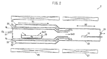
- FIG.2 is a vertical cross-sectional view showing a vapor phase deposition system 2 in the embodiment.
- the vapor phase deposition system 2 is a vapor phase deposition system using HVPE (Halide Vapor Phase Epitaxy) technique, and has a reaction chamber 20 having a first gas introducing port 21, a second gas introducing port 22, a third gas introducing port 23 and an exhaust port 24, and a first heating means 26 and a second heating means 27 which are placed around the reaction chamber 20 to heat predetermined regions in the reaction chamber 20.
- HVPE Hydrode Vapor Phase Epitaxy
- the growth rate when using the HVPE technique is higher than that in the PLD method, etc.
- in-plane distribution of film thickness is highly uniform and it is possible to grow a large-diameter film. Therefore, it is suitable for mass production of crystal.
- the reaction chamber 20 has a source reaction region R1 in which a reaction container 25 containing a Ga source is placed and a gallium source gas is produced, and a crystal growth region R2 in which the Ga 2 O 3 -based substrate 10 is placed and the ⁇ -Ga 2 O 3 -based single crystal film 12 is grown thereon.
- the reaction chamber 20 is formed of, e.g., quartz glass.
- reaction container 25 is formed of, e.g., quartz glass and the Ga source contained in the reaction container 25 is metal gallium.
- the first heating means 26 and the second heating means 27 are capable of respectively heating the source reaction region R1 and the crystal growth region R2 of the reaction chamber 20.
- the first heating means 26 and the second heating means 27 are, e.g., resistive heaters or radiation heaters.
- the first gas introducing port 21 is a port for introducing a Cl-containing gas (Cl 2 gas or HCl gas) into the source reaction region R1 of the reaction chamber 20 using an inert carrier gas (N 2 gas, Ar gas or He gas).
- the second gas introducing port 22 is a port for introducing an oxygen-containing gas (O 2 gas or H 2 O gas, etc.) as an oxygen source gas and a chloride gas (e.g., silicon tetrachloride, etc.) used to add a dopant such as Si to the ⁇ -Ga 2 O 3 -based single crystal film 12, into the crystal growth region R2 of the reaction chamber 20 using an inert carrier gas (N 2 gas, Ar gas or He gas).
- the third gas introducing port 23 is a port for introducing an inert carrier gas (N 2 gas, Ar gas or He gas) into the crystal growth region R2 of the reaction chamber 20.
- a process of growing the ⁇ -Ga 2 O 3 -based single crystal film 12 in the present embodiment will be described below as an example.
- the source reaction region R1 of the reaction chamber 20 is heated by the first heating means 26 and an atmosphere temperature in the source reaction region R1 is then maintained at a predetermined temperature.
- a Cl-containing gas introduced through the first gas introducing port 21 using a carrier gas is reacted with the metal gallium in the reaction container 25 at the above-mentioned atmosphere temperature, thereby producing a gallium chloride gas.
- the atmosphere temperature in the source reaction region R1 here is preferably a temperature at which GaCl gas has the highest partial pressure among component gases of the gallium chloride gas produced by the reaction of the metal gallium in the reaction container 25 with the Cl-containing gas.
- the gallium chloride gas here contains GaCl gas, GaCl 2 gas, GaCl 3 gas and (GaCl 3 ) 2 gas, etc.
- the temperature at which a driving force for growth of Ga 2 O 3 crystal is maintained is the highest with the GaCl gas among the gases contained in the gallium chloride gas. Growth at a high temperature is effective to obtain a high-quality Ga 2 O 3 crystal with high purity. Therefore, for growing the ⁇ -Ga 2 O 3 -based single crystal film 12, it is preferable to produce a gallium chloride gas in which a partial pressure of GaCl gas having a high driving force for growth at a high temperature is high.
- FIG.3 is a graph showing a relation, based on calculation of thermal equilibrium, between a driving force for growth and a growth temperature of Ga 2 O 3 crystal respectively when a gallium chloride gas consists of only a GaCl gas and consists of only a GaCl 3 gas.
- the calculation conditions are as follows: a carrier gas is, e.g., an inert gas such as N 2 , a furnace pressure is 1 atom, the supplied partial pressures of GaCl gas and GaCl 3 gas are both 1x10 -3 atom, and an O 2 /GaCl partial pressure ratio is 10.
- the horizontal axis indicates a growth temperature (°C) of Ga 2 O 3 crystal and the vertical axis indicates a driving force for crystal growth.
- the Ga 2 O 3 crystal grows more efficiently with a larger driving force for crystal growth.
- FIG.3 shows that the maximum temperature at which the driving force for growth is maintained is higher when using the GaCl gas as a Ga source gas than when using the GaCl 3 gas.
- FIG.4 is a graph showing a relation, based on calculation of thermal equilibrium, between an atmosphere temperature during reaction and equilibrium partial pressures of GaCl gas, GaCl 2 gas, GaCl 3 gas and (GaCl 3 ) 2 gas which are obtained by reaction of Ga with Cl 2 .
- the other calculation conditions are as follows: a carrier gas is, e.g., an inert gas such as N 2 , a furnace pressure is 1 atom and the supplied partial pressure of Cl 2 gas is 3x10 -3 atom.
- the horizontal axis indicates an atmosphere temperature (°C) and the vertical axis indicates an equilibrium partial pressure (atm). It is shown that more gas is produced at a higher equilibrium partial pressure.
- FIG.4 shows that when reacting the metal gallium chloride with the Cl-containing gas at an atmosphere temperature of about not less than 300°C, the equilibrium partial pressure of GaCl gas particularly capable of increasing a driving force for growth of Ga 2 O 3 crystal is increased, i.e., a partial pressure ratio of the GaCl gas with respect to the gallium chloride gas becomes higher. Based on this, it is preferable that the metal gallium in the reaction container 25 be reacted with the Cl-containing gas in a state that the atmosphere temperature in the source reaction region R1 is maintained at not less than 300°C by using the first heating means 26.
- the partial pressure ratio of the GaCl gas is predominantly high (the equilibrium partial pressure of the GaCl gas is four orders of magnitude greater than the GaCl 2 gas and is eight orders of magnitude greater than the GaCl 3 gas) and the gases other than GaCl gas hardly contribute to the growth of Ga 2 O 3 crystal.
- the metal gallium in the reaction container 25 be reacted with the Cl-containing gas in a state that the atmosphere temperature in the source reaction region R1 is maintained at not more than 1000 °C.
- the gallium chloride gas produced in the source reaction region R 1 is mixed with the oxygen-containing gas introduced through the second gas introducing port 22 and the Ga 2 O 3 -based substrate 10 is exposed to the mixed gas, thereby epitaxially growing the ⁇ -Ga 2 O 3 -based single crystal film 12 on the Ga 2 O 3 -based substrate 10.
- pressure in the crystal growth region R2 is maintained at, e.g., 1 atm.
- a source gas of the additive element e.g., a chloride gas such as silicon tetrachloride (SiCl 4 )
- SiCl 4 silicon tetrachloride
- FIG.5 is a graph showing a relation, based on calculation of thermal equilibrium, between an equilibrium partial pressure of GaCl and an O 2 /GaCl supplied partial pressure ratio when the atmosphere temperature during Ga 2 O 3 crystal growth is 1000°C.
- a ratio of the supplied partial pressure of the O 2 gas to the supplied partial pressure of the GaCl gas is referred to as "O 2 /GaCl supplied partial pressure ratio”. It is calculated using the supplied partial pressure value of the GaCl gas fixed to 1x10 -3 atom, a furnace pressure of 1 atom adjusted by using, e.g., an inert gas such as N 2 as a carrier gas, and various values of the O 2 gas supplied partial pressure.
- the horizontal axis indicates the O 2 /GaCl supplied partial pressure ratio and the vertical axis indicates an equilibrium partial pressure (atm) of the GaCl gas. It is shown that the smaller the supplied partial pressure of the GaCl gas, the more the GaCl gas is consumed for growth of Ga 2 O 3 crystal, i.e., the Ga 2 O 3 crystal grows efficiently.
- FIG.5 shows that the equilibrium partial pressure of the GaCl gas sharply falls at the O 2 /GaCl supplied partial pressure ratio of not less than 0.5 .
- the ⁇ -Ga 2 O 3 -based single crystal film 12 is preferably grown in a state that a ratio of the supplied partial pressure of the O 2 gas to the supplied partial pressure of the GaCl gas in the crystal growth region R2 is not less than 0.5 .
- FIG.6 is a graph showing X-ray diffraction spectra obtained by 2 ⁇ - ⁇ scan on crystalline layered structures in each of which a Ga 2 O 3 single crystal film is epitaxially grown on a ( 010 )-oriented principal surface of a ⁇ -Ga 2 O 3 substrate.
- the growth conditions are as follows: a furnace pressure is 1 atom, a carrier gas is N 2 gas, the GaCl supplied partial pressure is 5x10 -4 atom, and the O 2 /GaCl supplied partial pressure ratio is 5.
- the horizontal axis indicates an angle 2 ⁇ (degrees) formed between the incident direction and the reflected direction of X-ray and the vertical axis indicates diffraction intensity (arbitrary unit) of the X-ray.
- FIG.6 shows a spectrum from a ⁇ -Ga 2 O 3 substrate (without ⁇ -Ga 2 O 3 crystal film) and spectra from crystalline layered structures having ⁇ -Ga 2 O 3 crystal films respectively epitaxially grown at 800 °C, 850 °C, 900 °C, 950 °C, 1000 °C and 1050°C.
- the ⁇ -Ga 2 O 3 crystal films of these crystalline layered structures have a thickness of about 300 to 1000 nm.
- a ⁇ -Ga 2 O 3 single crystal film is obtained when a ⁇ -Ga 2 O 3 crystal film is grown at a growth temperature of not less than 900 °C.
- another Ga 2 O 3 -based substrate is used in place of the Ga 2 O 3 substrate or another Ga 2 O 3 -based crystal film is formed instead of the Ga 2 O 3 crystal film, evaluation results similar to those described above are obtained.
- the ⁇ -Ga 2 O 3 -based single crystal film 12 is obtained by growing at a growth temperature of not less than 900 °C.
- FIG.7 is a graph showing an X-ray diffraction spectrum obtained by 2 ⁇ - ⁇ scan on a crystalline layered structure in which a ⁇ -Ga 2 O 3 single crystal film is epitaxially grown on a (-201) -oriented principal surface of a ⁇ -Ga 2 O 3 substrate.
- the growth conditions for this ⁇ -Ga 2 O 3 single crystal film are as follows: a furnace pressure is 1 atom, a carrier gas is N 2 gas, the GaCl supplied partial pressure is 5x10 -4 atom, the O 2 /GaCl supplied partial pressure ratio is 5 and the growth temperature is 1000 °C.
- FIG.7 shows a spectrum from a ⁇ -Ga 2 O 3 substrate (without ⁇ -Ga 2 O 3 crystal film) having a (-201) -oriented principal surface and a spectrum from a crystalline layered structure having a ⁇ -Ga 2 O 3 crystal film epitaxially grown on the ⁇ -Ga 2 O 3 substrate at 1000 °C.
- the ⁇ -Ga 2 O 3 crystal film of this crystalline layered structure has a thickness of about 300 nm.
- FIG8 is a graph showing an X-ray diffraction spectrum obtained by 2 ⁇ - ⁇ scan on a crystalline layered structure in which a Ga 2 O 3 single crystal film is epitaxially grown on a ( 001 )-oriented principal surface of a ⁇ -Ga 2 O 3 substrate.
- the growth conditions for this ⁇ -Ga 2 O 3 single crystal film are as follows: a furnace pressure is 1 atom, a carrier gas is N 2 gas, the GaCl supplied partial pressure is 5x10 -4 atom, the O 2 /GaCl supplied partial pressure ratio is 5 and the growth temperature is 1000 °C.
- FIG.8 shows a spectrum from a ⁇ -Ga 2 O 3 substrate (without ⁇ -Ga 2 O 3 crystal film) having a ( 001 )-oriented principal surface and a spectrum from a crystalline layered structure having a ⁇ -Ga 2 O 3 crystal film epitaxially grown on the ⁇ -Ga 2 O 3 substrate at 1000 °C.
- the ⁇ -Ga 2 O 3 crystal film of this crystalline layered structure has a thickness of about 6 ⁇ m.
- FIG.9 is a graph showing an X-ray diffraction spectrum obtained by 2 ⁇ - ⁇ scan on a crystalline layered structure in which a Ga 2 O 3 single crystal film is epitaxially grown on a ( 101 )-oriented principal surface of a ⁇ -Ga 2 O 3 substrate.
- the growth conditions for this ⁇ -Ga 2 O 3 single crystal film are as follows: a furnace pressure is 1 atom, a carrier gas is N 2 gas, the GaCl supplied partial pressure is 5x10 -4 atom, the O 2 /GaCl supplied partial pressure ratio is 5 and the growth temperature is 1000 °C.
- FIG.9 shows a spectrum from a ⁇ -Ga 2 O 3 substrate (without ⁇ -Ga 2 O 3 crystal film) having a ( 101 )-oriented principal surface and a spectrum from a crystalline layered structure having a ⁇ -Ga 2 O 3 crystal film epitaxially grown on the ⁇ -Ga 2 O 3 substrate at 1000 °C.
- the ⁇ -Ga 2 O 3 crystal film of this crystalline layered structure has a thickness of about 4 ⁇ m.
- the horizontal axis indicates an angle 2 ⁇ (degrees) formed between the incident direction and the reflected direction of X-ray and the vertical axis indicates diffraction intensity (arbitrary unit) of the X-ray.
- FIGS.7 , 8 and 9 diffraction peaks of the spectrum from the crystalline layered structure having the ⁇ -Ga 2 O 3 crystal film grown at a growth temperature of 1000 °C are coincident with the diffraction peaks of the spectrum from the ⁇ -Ga 2 O 3 substrate.
- This result shows that a ⁇ -Ga 2 O 3 single crystal film is obtained when the ⁇ -Ga 2 O 3 crystal film is grown on the principal surface of the ⁇ -Ga 2 O 3 substrate having a plane orientation of ( 010 ), ( -201 ), ( 001 ) or ( 101 ) at a growth temperature of 1000 °C.
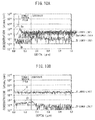
- FIGS.10A and 10B are graphs showing concentrations of impurities in the crystalline layered structure measured by secondary ion mass spectrometry (SIMS).
- the horizontal axis indicates a depth ( ⁇ m) of the crystalline layered structure from a principal surface 13 of the ⁇ -Ga 2 O 3 single crystal film and the vertical axis indicates concentration (atoms/cm 3 ) of each impurity.
- an interface between the ⁇ -Ga 2 O 3 substrate and the ⁇ -Ga 2 O 3 single crystal film is located at a depth of about 0.3 ⁇ m in the crystalline layered structure.
- horizontal arrows on the right side in FIGS.10A and 10B indicate the respective measurable lower limits of concentrations of the impurity elements.
- the 3-Ga 2 O 3 single crystal film of the crystalline layered structure used for the measurement is a film which is grown on the ( 010 )-oriented principal surface of the ⁇ -Ga 2 O 3 substrate at a growth temperature of 1000 °C.
- FIG.10A shows the concentrations of C, Sn, and Si in the crystalline layered structure and FIG.10B shows the concentrations of H and Cl in the crystalline layered structure.
- the concentration of each impurity element in the ⁇ -Ga 2 O 3 single crystal film is close to the measurable lower limit and is almost unchanged from the concentration in the Ga 2 O 3 substrate. This shows that the ⁇ -Ga 2 O 3 single crystal film is a highly pure film.
- not more than about 5x10 16 (atoms/cm 3 ) of Cl is contained in the ⁇ -Ga 2 O 3 single crystal film.
- the Ga 2 O 3 single crystal film is formed by the HVPE method using Cl-containing gas.
- Cl-containing gas is not used to form a Ga 2 O 3 single crystal film when using a method other than the HVPE method, and the Ga 2 O 3 single crystal film does not contain Cl, or at least does not contain 1x10 16 (atoms/cm 3 ) or more of Cl.
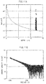
- FIG.11A is a graph showing a carrier concentration profile in a depth direction of the crystalline layered structure in which a ⁇ -Ga 2 O 3 crystal film is epitaxially grown on a ( 001 )-oriented principal surface of a ⁇ -Ga 2 O 3 substrate.
- the horizontal axis indicates a depth ( ⁇ m) from the surface of the ⁇ -Ga 2 O 3 crystal film and the vertical axis indicates a carrier concentration, i.e., a difference (cm -3 ) between a donor concentration N d as a net donor concentration and an acceptor concentration N a .
- a dotted curved line in the drawing is a theoretical curve showing a relation between the donor concentration and depletion layer thickness when relative permittivity of ⁇ -Ga 2 O 3 is 10 and built-in potential of ⁇ -Ga 2 O 3 in contact with Pt is 1.5 V.
- the procedure used to obtain the data shown in FIG.11A is as follows. Firstly, an undoped ⁇ -Ga 2 O 3 crystal film having a thickness of about 15 ⁇ m is epitaxially grown on an Sn-doped n-type ⁇ -Ga 2 O 3 substrate having a ( 001 )-oriented principal surface by the HVPE method. "Undoped” here means that intentional doping is not carried out, and it does not deny the presence of unintentional impurities.
- the ⁇ -Ga 2 O 3 substrate is a 10 mm-square substrate having a thickness of 600 ⁇ m and has a carrier concentration of about 6x10 18 cm -3 .
- the growth conditions for this ⁇ -Ga 2 O 3 single crystal film are as follows: a furnace pressure is 1 atom, a carrier gas is N 2 gas, the GaCl supplied partial pressure is 5x10 -4 atom, the O 2 /GaCl supplied partial pressure ratio is 5 and the growth temperature is 1000 °C.
- the surface of the undoped ⁇ -Ga 2 O 3 crystal film is polished 3 ⁇ m by CMP to flatten the surface.
- a Schottky electrode is formed on the ⁇ -Ga 2 O 3 crystal film and an ohmic electrode on the ⁇ -Ga 2 O 3 substrate, and C-V measurement is conducted while changing bias voltage in a range of +0 to - 10 V. Then, a carrier concentration profile in a depth direction is calculated based on the C-V measurement result.
- the Schottky electrode here is an 800 ⁇ m-diameter circular electrode having a laminated structure in which a 15 nm-thick Pt film, a 5 nm-thick Ti film and a 250 nm-thick Au film are laminated in this order.
- the ohmic electrode is a 10 mm-square electrode having a laminated structure in which a 50 nm-thick Ti film and a 300 nm-thick Au film are laminated in this order.
- FIG.11A no measurement point is present in a region shallower than 12 ⁇ m which is equal to the thickness of the ⁇ -Ga 2 O 3 crystal film, and all measurement points are 12 ⁇ m on the horizontal axis. This shows that the entire region of the ⁇ -Ga 2 O 3 crystal film is depleted in the bias voltage range of + 0 to - 10 V.
- the entire region of the ⁇ -Ga 2 O 3 crystal film is naturally depleted at the bias voltage of 0. It is predicted that the residual carrier concentration in the ⁇ -Ga 2 O 3 crystal film is as very small as not more than 1x10 13 cm -3 since the donor concentration is about 1x10 13 cm -3 when the depletion layer thickness is 12 ⁇ m, based on the theoretical curve.
- the residual carrier concentration in the ⁇ -Ga 2 O 3 crystal film is not more than 1x10 13 cm -3 , for example, it is possible to control the carrier concentration in the ⁇ -Ga 2 O 3 crystal film in a range of 1x10 13 to 1x10 20 cm -3 by doping a IV group element.
- FIG.11B is a graph showing voltage endurance characteristics of the above-mentioned crystalline layered structure.
- the horizontal axis indicates applied voltage (V) and the vertical axis indicates current density (A/cm 2 ).
- a dotted straight line in the drawing indicates the measurable lower limit value.
- the procedure used to obtain the data shown in FIG.11B is as follows. Firstly, the above-mentioned crystalline layered structure composed of a ⁇ -Ga 2 O 3 substrate and a ⁇ -Ga 2 O 3 crystal film is prepared.
- a Schottky electrode is formed on the ⁇ -Ga 2 O 3 crystal film and an ohmic electrode on the ⁇ -Ga 2 O 3 substrate, and current density at an applied voltage of 1000 V is measured.
- the Schottky electrode here is a 200 ⁇ m-diameter circular electrode having a laminated structure in which a 15 nm-thick Pt film, a 5 nm-thick Ti film and a 250 nm-thickAu film are laminated in this order.
- the ohmic electrode is a 10 mm-square electrode having a laminated structure in which a 50 nm-thick Ti film and a 300 nm-thick Au film are laminated in this order.
- FIG.11B shows that, even when voltage of 1000 V is applied to the crystalline layered structure, leakage current is as very small as about 1x10 -5 A/cm 2 and insulation breakdown does not occur. This result is considered to be due to that the ⁇ -Ga 2 O 3 crystal film is a high-quality crystal film with only few crystal defects and the donor concentration is low.
- FIG.12 is a graph showing a carrier concentration profile in a depth direction of the crystalline layered structure in which a ⁇ -Ga 2 O 3 crystal film is epitaxially grown on a ( 010 )-oriented principal surface of a ⁇ -Ga 2 O 3 substrate.
- the horizontal axis indicates a depth ( ⁇ m) from the surface of the ⁇ -Ga 2 O 3 crystal film and the vertical axis indicates a carrier concentration, i.e., a difference (cm -3 ) between a donor concentration N d as a net donor concentration and an acceptor concentration N a .
- a dotted curved line in the drawing is a theoretical curve showing a relation between the donor concentration and depletion layer thickness when relative permittivity of ⁇ -Ga 2 O 3 is 10 and built-in potential of ⁇ -Ga 2 O 3 in contact with Pt is 1.5 V.
- the procedure used to obtain the data shown in FIG.12 is as follows. Firstly, an undoped ⁇ -Ga 2 O 3 crystal film having a thickness of about 0.9 ⁇ m is epitaxially grown on an Sn-doped n-type ⁇ -Ga 2 O 3 substrate having a ( 010 )-oriented principal surface by the HVPE method.
- the ⁇ -Ga 2 O 3 substrate is a 10 mm-square substrate having a thickness of 600 ⁇ m and has a carrier concentration of about 6x10 18 cm -3 .
- the growth conditions for this ⁇ -Ga 2 O 3 single crystal film are as follows: a furnace pressure is 1 atom, a carrier gas is N 2 gas. the GaCl supplied partial pressure is 5x10 -4 atom, the O 2 /GaCl supplied partial pressure ratio is 5 and the growth temperature is 1000 °C.
- a Schottky electrode is formed on the undoped ⁇ -Ga 2 O 3 crystal film and an ohmic electrode on the ⁇ -Ga 2 O 3 substrate, and C-V measurement is conducted while changing bias voltage in a range of +0 to - 10 V. Then, a carrier concentration profile in a depth direction is calculated based on the C-V measurement result.
- the Schottky electrode here is a 400 ⁇ m-diameter circular electrode having a laminated structure in which a 15 nm-thick Pt film, a 5 nm-thick Ti film and a 250 nm-thick Au film are laminated in this order.
- the ohmic electrode is a 10 mm-square electrode having a laminated structure in which a 50 nm-thick Ti film and a 300 nm-thick Au film are laminated in this order.
- measurement points at a bias voltage of 0 are 0.85 ⁇ m on the horizontal axis (measurement points in a region deeper than 0.85 ⁇ m are measurement points when the bias voltage is close to 10 V). It is predicted that the residual carrier concentration in the ⁇ -Ga 2 O 3 crystal film is as very small as not more than 3x10 15 cm -3 since the donor concentration is about 2.3x10 15 cm -3 when the depletion layer thickness is 0.85 ⁇ m, based on the theoretical curve.
- the embodiment by controlling the conditions of producing the gallium source gas and the growth conditions for the ⁇ -Ga 2 O 3 -based single crystal film in the HVPE method, it is possible to efficiently grow a high-quality and large-diameter ⁇ -Ga 2 O 3 -based single crystal film.
- the ⁇ -Ga 2 O 3 -based single crystal film has excellent crystal quality, it is possible to grow a good-quality crystal film on the ⁇ -Ga 2 O 3 -based single crystal film.
- a high-quality semiconductor device can be manufactured by using the crystalline layered structure including the ⁇ -Ga 2 O 3 -based single crystal film in the present embodiment.
- a method for efficiently growing a high-quality, large diameter ⁇ -Ga 2 O 3 -based single crystal film, and a crystalline layered structure having a ⁇ -Ga 2 O 3 -based single crystal film grown using this growing method are provided.
Landscapes
- Chemical & Material Sciences (AREA)
- Engineering & Computer Science (AREA)
- Materials Engineering (AREA)
- Metallurgy (AREA)
- Organic Chemistry (AREA)
- General Chemical & Material Sciences (AREA)
- Chemical Kinetics & Catalysis (AREA)
- Crystallography & Structural Chemistry (AREA)
- Inorganic Chemistry (AREA)
- Mechanical Engineering (AREA)
- Electrochemistry (AREA)
- Crystals, And After-Treatments Of Crystals (AREA)
Abstract
Description
- The invention relates to a method for growing a β-Ga2O3-based single crystal film and a crystalline layered structure.
- The MBE (Molecular Beam Epitaxy) method and the PLD (Pulsed Laser Deposition) method are known as a growth method of β-Ga2O3 single crystal film (see, e.g.,
PTL 1 and PTL 2). Other growth methods thereof, the sol-gel process, the MOCVD (Metal Organic Chemical Vapor Deposition) process and the mist CVD process are also known. -
- [PTL 1] JP-A-2013-56803
- [PTL 2] JP-B-4565062
- The MBE method is conducted, however, such that crystal is grown in a high vacuum chamber. Thus, it is difficult to increase the diameter of a β-Ga2O3 single crystal film. Although a high-quality film can be generally obtained by increasing the growth temperature, a sufficient film growth rate is not obtained due to an increase in re-evaporation of source gases and it is thus not suitable for mass production.
- The PLD method is not suitable for growing a film with a large area since a source (a raw material supply source to a substrate) is a point source which causes a growth rate to be different between a portion immediately above the source and other portions and in-plane distribution of film thickness is likely to be non-uniform. In addition, it takes long time to form a thick film due to a low film growth rate, hence, not suitable for mass production.
- In regard to the sol-gel method, the MOCVD method and the mist CVD method, it is relatively easy to increase a diameter but it is difficult to obtain single crystal films with high purity since impurities contained in the used materials are incorporated into the β-Ga2O3 single crystal film during epitaxial growth.
- Thus, it is an object of the invention to provide a method for growing a β-Ga2O3-based single crystal film that allows a high-quality and large-diameter β-Ga2O3-based single crystal film to grow efficiently, as well as a crystalline layered structure having the β-Ga2O3-based single crystal film grown by the method.
- According to an embodiment of the invention, in order to achieve the object, a growth method of a β-Ga2O3-based single crystal film defined by [1] to [8] below will be provided.
- [1] A method for growing a β-Ga2O3-based single crystal film by HVPE method, comprising a step of exposing a Ga2O3-based substrate to a gallium chloride-based gas and an oxygen-including gas and growing a β-Ga2O3-based single crystal film on a principal surface of the Ga2O3-based substrate at a growth temperature of not lower than 900°C.
- [2] The method for growing a β-Ga2O3-based single crystal film defined by [1]. wherein the gallium chloride-based gas is produced by reacting a gallium source with a Cl-including gas comprising a Cl2 gas or an HCl gas.
- [3] The method for growing a β-Ga2O3-based single crystal film defined by [1] or [2], wherein in the gallium chloride-based gas a GaCl gas has a highest partial pressure ratio.
- [4] The method for growing a β-Ga2O3-based single crystal film defined by [1 or [2], wherein the oxygen-including gas comprises an O2 gas.
- [5] The method for growing a β-Ga2O3-based single crystal film defined by [2], wherein the Cl-including gas comprises a Cl2 gas.
- [6] The method for growing a β-Ga2O3-based single crystal film defined by [1] or [2], wherein a ratio of a supplied partial pressure of the oxygen-including gas to a supplied partial pressure of the gallium chloride-based gas when growing the β-Ga2O3-based single crystal film is not more than 0.5.
- [7] The method for growing a β-Ga2O3-based single crystal film defined by [1] or [2], wherein the principal surface of the Ga2O3-based substrate has a plane orientation of (010), (-201), (001) or (101).
- [8] The method for growing a β-Ga2O3-based single crystal film defined by [1] or [2], wherein the gallium chloride-based gas is produced at an atmosphere temperature of not less than 300°C.
According to another embodiment of the invention, in order to achieve the object, a crystalline layered structure defined by [9] to [12] below will be provided. - [9] A crystalline layered structure, comprising:
- a Ga2O3-based substrate; and
- a β-Ga2O3-based single crystal film that is formed on a principal surface of the Ga2O3-based substrate by epitaxial crystal growth and includes Cl.
- [10] The crystalline layered structure defined by [9], wherein a Cl concentration in the β-Ga2O3-based single crystal film is not more than 5x10¹⁶ atoms/cm3.
- [11] The crystalline layered structure defined by [9] or [10], wherein the β-Ga2O3-based single crystal film comprises a β-Ga2O3 crystal film.
- [12] The crystalline layered structure defined by [11], wherein a residual carrier concentration in the β-Ga2O3-based single crystal film is not more than 3x10¹⁵ atoms/cm3.
- According to the invention, a method for growing a β-Ga2O3-based single crystal film can be provided that allows a high-quality and large-diameter β-Ga2O3-based single crystal film to grow efficiently, as well as a crystalline layered structure having the β-Ga2O3-based single crystal film grown by the method.
-
- [
FIG:1] FIG.1 is a vertical cross-sectional view showing a crystalline layered structure in an embodiment. - [
FIG.2] FIG.2 is a vertical cross-sectional view showing a vapor phase deposition system in the embodiment. - [
FIG.3] FIG.3 is a graph showing a relation, based on calculation of thermal equilibrium, between a driving force for growth and a growth temperature of Ga2O3 crystal in the case that a gallium chloride gas is only of a GaCl gas and a GaCl3 gas, respectively. - [
FIG.4] FIG4 is a graph showing a relation, based on calculation of thermal equilibrium, between an atmosphere temperature and equilibrium partial pressures of GaCl gas, GaCl2 gas, GaCl3 gas and (GaCl3)2 gas which are obtained by reaction of Ga with Cl2. - [
FIG.5] FIG.5 is a graph showing a relation, based on calculation of thermal equilibrium, between equilibrium partial pressure of GaCl and an O2/GaCl supplied partial pressure ratio when the atmosphere temperature during Ga2O3 crystal growth is 1000°C. - [
FIG.6] FIG.6 is a graph showing X-ray diffraction spectra obtained by 2θ-ω scan on crystalline layered structure in each of which a Ga2O3 single crystal film is epitaxially grown on a (010)-oriented principal surface of a Ga2O3 substrate. - [
FIG.7] FIG.7 is a graph showing an X-ray diffraction spectrum obtained by 2θ-ω scan on a crystalline layered structure in which a Ga2O3 single crystal film is epitaxially grown on a (-201)-oriented principal surface of a Ga2O3 substrate at 1000°C. - [
FIG.8] FIG.8 is a graph showing an X-ray diffraction spectrum obtained by 2θ-ω scan on a crystalline layered structure in which a Ga2O3 single crystal film is epitaxially grown on a (001)-oriented principal surface of a β-Ga2O3 substrate. - [
FIG.9] FIG.9 is a graph showing an X-ray diffraction spectrum obtained by 2θ-ω scan on a crystalline layered structure in which a Ga2O3 single crystal film is epitaxially grown on a (101)-oriented principal surface of a β-Ga2O3 substrate. - [
FIG.10A] FIG.10A is a graph showing the concentration of impurities in the crystalline layered structure measured by secondary ion mass spectrometry (SIMS). - [
FIG.10B] FIG.10B is a graph showing the concentration of impurities in the crystalline layered structure measured by secondary ion mass spectrometry (SIMS). - [
FIG.11A] FIG.11A is a graph showing the carrier concentration profile in a depth direction of the crystalline layered structure in which a β-Ga2O3 crystal film is epitaxially grown on a (001)-oriented principal surface of a β-Ga2O3 substrate. - [
FIG.11B] FIG.11B is a graph showing the voltage endurance characteristics of the crystalline layered structure in which a β-Ga2O3 crystal film is epitaxially grown on a (001)-oriented principal surface of a β-Ga2O3 substrate. - [
FIG.12] FIG.12 is a graph showing a carrier concentration profile in a depth direction of the crystalline layered structure in which a β-Ga2O3 crystal film is epitaxially grown on a (010)-oriented principal surface of a β-Ga2O3 substrate. -
FIG.1 is a vertical cross-sectional view showing a crystallinelayered structure 1 in an embodiment. The crystallinelayered structure 1 has a Ga2O3-basedsubstrate 10 and a β-Ga2O3-basedsingle crystal film 12 formed on aprincipal surface 11 of the Ga2O3-basedsubstrate 10 by epitaxial crystal growth. - The Ga2O3-based
substrate 10 is a substrate formed of a Ga2O3-based single crystal with a β-crystal structure. The Ga2O3-based single crystal here means a Ga2O3 single crystal or is a Ga2O3 single crystal doped with an element such as A1 or In, and may be, e.g., a (GaxAlyIn(1-x-y))2O3 (0<x≤1, 0≤y≤1, 0<x+y≤1) single crystal which is a Ga2O3 single crystal doped with Al and In. The band gap is widened by adding Al and is narrowed by adding In. In addition, the Ga2O3-basedsubstrate 10 may contain a conductive impurity such as Si. - The plane orientation of the
principal surface 11 of the Ga2O3-basedsubstrate 10 is, e.g., (010), (-201), (001) or (101). - To form the Ga2O3-based
substrate 10, for example, a bulk crystal of a Ga2O3-based single crystal grown by, e.g., a melt-growth technique such as the FZ (Floating Zone) method or the EFG (Edge Defined Film Fed Growth) method is sliced and the surface thereof is then polished. - The β-Ga2O3-based
single crystal film 12 is formed of a Ga2O3-based single crystal with a β-crystal structure in the same manner as the Ga2O3-basedsubstrate 10. In addition, the β-Ga2O3-basedsingle crystal film 12 may contain a conductive impurity such as Si. - A structure of a vapor phase deposition system used for growing the β-Ga2O3-based
single crystal film 12 in the present embodiment will be described below as an example. -
FIG.2 is a vertical cross-sectional view showing a vaporphase deposition system 2 in the embodiment. The vaporphase deposition system 2 is a vapor phase deposition system using HVPE (Halide Vapor Phase Epitaxy) technique, and has areaction chamber 20 having a firstgas introducing port 21, a secondgas introducing port 22, a thirdgas introducing port 23 and anexhaust port 24, and a first heating means 26 and a second heating means 27 which are placed around thereaction chamber 20 to heat predetermined regions in thereaction chamber 20. - The growth rate when using the HVPE technique is higher than that in the PLD method, etc. In addition, in-plane distribution of film thickness is highly uniform and it is possible to grow a large-diameter film. Therefore, it is suitable for mass production of crystal.
- The
reaction chamber 20 has a source reaction region R1 in which areaction container 25 containing a Ga source is placed and a gallium source gas is produced, and a crystal growth region R2 in which the Ga2O3-basedsubstrate 10 is placed and the β-Ga2O3-basedsingle crystal film 12 is grown thereon. Thereaction chamber 20 is formed of, e.g., quartz glass. - Here, the
reaction container 25 is formed of, e.g., quartz glass and the Ga source contained in thereaction container 25 is metal gallium. - The first heating means 26 and the second heating means 27 are capable of respectively heating the source reaction region R1 and the crystal growth region R2 of the
reaction chamber 20. The first heating means 26 and the second heating means 27 are, e.g., resistive heaters or radiation heaters. - The first
gas introducing port 21 is a port for introducing a Cl-containing gas (Cl2 gas or HCl gas) into the source reaction region R1 of thereaction chamber 20 using an inert carrier gas (N2 gas, Ar gas or He gas). The secondgas introducing port 22 is a port for introducing an oxygen-containing gas (O2 gas or H2O gas, etc.) as an oxygen source gas and a chloride gas (e.g., silicon tetrachloride, etc.) used to add a dopant such as Si to the β-Ga2O3-basedsingle crystal film 12, into the crystal growth region R2 of thereaction chamber 20 using an inert carrier gas (N2 gas, Ar gas or He gas). The thirdgas introducing port 23 is a port for introducing an inert carrier gas (N2 gas, Ar gas or He gas) into the crystal growth region R2 of thereaction chamber 20. - A process of growing the β-Ga2O3-based
single crystal film 12 in the present embodiment will be described below as an example. - Firstly, the source reaction region R1 of the
reaction chamber 20 is heated by the first heating means 26 and an atmosphere temperature in the source reaction region R1 is then maintained at a predetermined temperature. - Next, in the source reaction region R1, a Cl-containing gas introduced through the first
gas introducing port 21 using a carrier gas is reacted with the metal gallium in thereaction container 25 at the above-mentioned atmosphere temperature, thereby producing a gallium chloride gas. - The atmosphere temperature in the source reaction region R1 here is preferably a temperature at which GaCl gas has the highest partial pressure among component gases of the gallium chloride gas produced by the reaction of the metal gallium in the
reaction container 25 with the Cl-containing gas. The gallium chloride gas here contains GaCl gas, GaCl2 gas, GaCl3 gas and (GaCl3)2 gas, etc. - The temperature at which a driving force for growth of Ga2O3 crystal is maintained is the highest with the GaCl gas among the gases contained in the gallium chloride gas. Growth at a high temperature is effective to obtain a high-quality Ga2O3 crystal with high purity. Therefore, for growing the β-Ga2O3-based
single crystal film 12, it is preferable to produce a gallium chloride gas in which a partial pressure of GaCl gas having a high driving force for growth at a high temperature is high. -
FIG.3 is a graph showing a relation, based on calculation of thermal equilibrium, between a driving force for growth and a growth temperature of Ga2O3 crystal respectively when a gallium chloride gas consists of only a GaCl gas and consists of only a GaCl3 gas. The calculation conditions are as follows: a carrier gas is, e.g., an inert gas such as N2, a furnace pressure is 1 atom, the supplied partial pressures of GaCl gas and GaCl3 gas are both 1x10⁻³ atom, and an O2/GaCl partial pressure ratio is 10. - In
FIG.3 , the horizontal axis indicates a growth temperature (°C) of Ga2O3 crystal and the vertical axis indicates a driving force for crystal growth. The Ga2O3 crystal grows more efficiently with a larger driving force for crystal growth. -
FIG.3 shows that the maximum temperature at which the driving force for growth is maintained is higher when using the GaCl gas as a Ga source gas than when using the GaCl3 gas. - If hydrogen is contained in an atmosphere for growing the β-Ga2O3-based
single crystal film 12, surface flatness and a driving force for growth of the β-Ga2O3-basedsingle crystal film 12 decrease. Therefore, it is preferable that a Cl2 gas not containing hydrogen be used as the Cl-containing gas. -
FIG.4 is a graph showing a relation, based on calculation of thermal equilibrium, between an atmosphere temperature during reaction and equilibrium partial pressures of GaCl gas, GaCl2 gas, GaCl3 gas and (GaCl3)2 gas which are obtained by reaction of Ga with Cl2. The other calculation conditions are as follows: a carrier gas is, e.g., an inert gas such as N2, a furnace pressure is 1 atom and the supplied partial pressure of Cl2 gas is 3x10⁻³ atom. - In
FIG.4 , the horizontal axis indicates an atmosphere temperature (°C) and the vertical axis indicates an equilibrium partial pressure (atm). It is shown that more gas is produced at a higher equilibrium partial pressure. -
FIG.4 shows that when reacting the metal gallium chloride with the Cl-containing gas at an atmosphere temperature of about not less than 300°C, the equilibrium partial pressure of GaCl gas particularly capable of increasing a driving force for growth of Ga2O3 crystal is increased, i.e., a partial pressure ratio of the GaCl gas with respect to the gallium chloride gas becomes higher. Based on this, it is preferable that the metal gallium in thereaction container 25 be reacted with the Cl-containing gas in a state that the atmosphere temperature in the source reaction region R1 is maintained at not less than 300°C by using the first heating means 26. - Also, at the atmosphere temperature of, e.g., 850°C, the partial pressure ratio of the GaCl gas is predominantly high (the equilibrium partial pressure of the GaCl gas is four orders of magnitude greater than the GaCl2 gas and is eight orders of magnitude greater than the GaCl3 gas) and the gases other than GaCl gas hardly contribute to the growth of Ga2O3 crystal.
- Meanwhile, in consideration of the lifetime of the first heating means 26 and heat resistance of the
reaction chamber 20 formed of quartz glass, etc., it is preferable that the metal gallium in thereaction container 25 be reacted with the Cl-containing gas in a state that the atmosphere temperature in the source reaction region R1 is maintained at not more than 1000°C. - Next, in the crystal growth region R2, the gallium chloride gas produced in the source reaction region R1 is mixed with the oxygen-containing gas introduced through the second
gas introducing port 22 and the Ga2O3-basedsubstrate 10 is exposed to the mixed gas, thereby epitaxially growing the β-Ga2O3-basedsingle crystal film 12 on the Ga2O3-basedsubstrate 10. At this time, in a furnace housing thereaction chamber 20, pressure in the crystal growth region R2 is maintained at, e.g., 1 atm. - When forming the β-Ga2O3-based
single crystal film 12 containing an additive element such as Si or Al, a source gas of the additive element (e.g., a chloride gas such as silicon tetrachloride (SiCl4)) is introduced, together with the gallium chloride gas and the oxygen-containing gas, into the crystal growth region R2 through thegas introducing port 22. - If hydrogen is contained in an atmosphere for growing the p-Ga2O3-based
single crystal film 12, surface flatness and a driving force for growth of the β-Ga2O3-basedsingle crystal film 12 decrease. Therefore, it is preferable that an O2 gas not containing hydrogen be used as the oxygen-containing gas. -
FIG.5 is a graph showing a relation, based on calculation of thermal equilibrium, between an equilibrium partial pressure of GaCl and an O2/GaCl supplied partial pressure ratio when the atmosphere temperature during Ga2O3 crystal growth is 1000°C. Here, a ratio of the supplied partial pressure of the O2 gas to the supplied partial pressure of the GaCl gas is referred to as "O2/GaCl supplied partial pressure ratio". It is calculated using the supplied partial pressure value of the GaCl gas fixed to 1x10⁻³ atom, a furnace pressure of 1 atom adjusted by using, e.g., an inert gas such as N2 as a carrier gas, and various values of the O2 gas supplied partial pressure. - In
FIG.5 , the horizontal axis indicates the O2/GaCl supplied partial pressure ratio and the vertical axis indicates an equilibrium partial pressure (atm) of the GaCl gas. It is shown that the smaller the supplied partial pressure of the GaCl gas, the more the GaCl gas is consumed for growth of Ga2O3 crystal, i.e., the Ga2O3 crystal grows efficiently. -
FIG.5 shows that the equilibrium partial pressure of the GaCl gas sharply falls at the O2/GaCl supplied partial pressure ratio of not less than 0.5. - Based on this, to efficiently grow the β-Ga2O3-based
single crystal film 12, the β-Ga2O3-basedsingle crystal film 12 is preferably grown in a state that a ratio of the supplied partial pressure of the O2 gas to the supplied partial pressure of the GaCl gas in the crystal growth region R2 is not less than 0.5. -
FIG.6 is a graph showing X-ray diffraction spectra obtained by 2θ-ω scan on crystalline layered structures in each of which a Ga2O3 single crystal film is epitaxially grown on a (010)-oriented principal surface of a β-Ga2O3 substrate. The growth conditions are as follows: a furnace pressure is 1 atom, a carrier gas is N2 gas, the GaCl supplied partial pressure is 5x10⁻⁴ atom, and the O2/GaCl supplied partial pressure ratio is 5. - In
FIG.6 , the horizontal axis indicates an angle 2θ (degrees) formed between the incident direction and the reflected direction of X-ray and the vertical axis indicates diffraction intensity (arbitrary unit) of the X-ray. -
FIG.6 shows a spectrum from a β-Ga2O3 substrate (without β-Ga2O3 crystal film) and spectra from crystalline layered structures having β-Ga2O3 crystal films respectively epitaxially grown at 800°C, 850°C, 900°C, 950°C, 1000°C and 1050°C. The β-Ga2O3 crystal films of these crystalline layered structures have a thickness of about 300 to 1000 nm. - Diffraction peaks from a (-313) plane, a (-204) plane and a (-712) plane or a (512) plane resulting from the presence of non-oriented grains, which are observed in the spectra from the crystalline layered structures having the β-Ga2O3 crystal films grown at growth temperatures of 800°C and 850°C, disappear in the spectra from the crystalline layered structures having the β-Ga2O3 crystal films grown at growth temperatures of not less than 900°C. This shows that a β-Ga2O3 single crystal film is obtained when a Ga2O3 single crystal film is grown at a growth temperature of not less than 900°C.
- Also in case that the principal surface of the β-Ga2O3 substrate has a plane orientation of (-201), (001) or (101), a β-Ga2O3 single crystal film is obtained when a β-Ga2O3 crystal film is grown at a growth temperature of not less than 900°C. In addition, also in case that another Ga2O3-based substrate is used in place of the Ga2O3 substrate or another Ga2O3-based crystal film is formed instead of the Ga2O3 crystal film, evaluation results similar to those described above are obtained. In other words, when the plane orientation of the principal surface of the Ga2O3-based
substrate 10 is (010), (-201), (001) or (101), the β-Ga2O3-basedsingle crystal film 12 is obtained by growing at a growth temperature of not less than 900°C. -
FIG.7 is a graph showing an X-ray diffraction spectrum obtained by 2θ-ω scan on a crystalline layered structure in which a β-Ga2O3 single crystal film is epitaxially grown on a (-201)-oriented principal surface of a β-Ga2O3 substrate. The growth conditions for this β-Ga2O3 single crystal film are as follows: a furnace pressure is 1 atom, a carrier gas is N2 gas, the GaCl supplied partial pressure is 5x10⁻⁴ atom, the O2/GaCl supplied partial pressure ratio is 5 and the growth temperature is 1000°C. -
FIG.7 shows a spectrum from a β-Ga2O3 substrate (without β-Ga2O3 crystal film) having a (-201)-oriented principal surface and a spectrum from a crystalline layered structure having a β-Ga2O3 crystal film epitaxially grown on the β-Ga2O3 substrate at 1000°C. The β-Ga2O3 crystal film of this crystalline layered structure has a thickness of about 300 nm. -
FIG8 is a graph showing an X-ray diffraction spectrum obtained by 2θ-ω scan on a crystalline layered structure in which a Ga2O3 single crystal film is epitaxially grown on a (001)-oriented principal surface of a β-Ga2O3 substrate. The growth conditions for this β-Ga2O3 single crystal film are as follows: a furnace pressure is 1 atom, a carrier gas is N2 gas, the GaCl supplied partial pressure is 5x10⁻⁴ atom, the O2/GaCl supplied partial pressure ratio is 5 and the growth temperature is 1000°C. -
FIG.8 shows a spectrum from a β-Ga2O3 substrate (without β-Ga2O3 crystal film) having a (001)-oriented principal surface and a spectrum from a crystalline layered structure having a β-Ga2O3 crystal film epitaxially grown on the β-Ga2O3 substrate at 1000°C. The β-Ga2O3 crystal film of this crystalline layered structure has a thickness of about 6 µm. -
FIG.9 is a graph showing an X-ray diffraction spectrum obtained by 2θ-ω scan on a crystalline layered structure in which a Ga2O3 single crystal film is epitaxially grown on a (101)-oriented principal surface of a β-Ga2O3 substrate. The growth conditions for this β-Ga2O3 single crystal film are as follows: a furnace pressure is 1 atom, a carrier gas is N2 gas, the GaCl supplied partial pressure is 5x10⁻⁴ atom, the O2/GaCl supplied partial pressure ratio is 5 and the growth temperature is 1000°C. -
FIG.9 shows a spectrum from a β-Ga2O3 substrate (without β-Ga2O3 crystal film) having a (101)-oriented principal surface and a spectrum from a crystalline layered structure having a β-Ga2O3 crystal film epitaxially grown on the β-Ga2O3 substrate at 1000°C. The β-Ga2O3 crystal film of this crystalline layered structure has a thickness of about 4 µm. - In
FIGS.7 ,8 and9 , the horizontal axis indicates an angle 2θ (degrees) formed between the incident direction and the reflected direction of X-ray and the vertical axis indicates diffraction intensity (arbitrary unit) of the X-ray. - In
FIGS.7 ,8 and9 , diffraction peaks of the spectrum from the crystalline layered structure having the β-Ga2O3 crystal film grown at a growth temperature of 1000°C are coincident with the diffraction peaks of the spectrum from the β-Ga2O3 substrate. This result shows that a β-Ga2O3 single crystal film is obtained when the β-Ga2O3 crystal film is grown on the principal surface of the β-Ga2O3 substrate having a plane orientation of (010), (-201), (001) or (101) at a growth temperature of 1000°C. -
FIGS.10A and 10B are graphs showing concentrations of impurities in the crystalline layered structure measured by secondary ion mass spectrometry (SIMS). - In
FIGS.10A and 10B , the horizontal axis indicates a depth (µm) of the crystalline layered structure from aprincipal surface 13 of the β-Ga2O3 single crystal film and the vertical axis indicates concentration (atoms/cm3) of each impurity. Here, an interface between the β-Ga2O3 substrate and the β-Ga2O3 single crystal film is located at a depth of about 0.3 µm in the crystalline layered structure. In addition, horizontal arrows on the right side inFIGS.10A and 10B indicate the respective measurable lower limits of concentrations of the impurity elements. - The 3-Ga2O3 single crystal film of the crystalline layered structure used for the measurement is a film which is grown on the (010)-oriented principal surface of the β-Ga2O3 substrate at a growth temperature of 1000°C.
-
FIG.10A shows the concentrations of C, Sn, and Si in the crystalline layered structure andFIG.10B shows the concentrations of H and Cl in the crystalline layered structure. According toFIGS.10A and 10B , the concentration of each impurity element in the β-Ga2O3 single crystal film is close to the measurable lower limit and is almost unchanged from the concentration in the Ga2O3 substrate. This shows that the β-Ga2O3 single crystal film is a highly pure film. - Similar evaluation results are obtained also in case that the principal surface of the β-Ga2O3 substrate has a plane orientation of (-201), (101) or (001). In addition, also in case that another Ga2O3-based substrate is used in place of the β-Ga2O3 substrate or another Ga2O3-based single crystal film is formed instead of the β-Ga2O3 single crystal film, evaluation results similar to those described above are obtained.
- According to
FIG.10B , not more than about 5x10¹⁶ (atoms/cm3) of Cl is contained in the β-Ga2O3 single crystal film. This results from that the Ga2O3 single crystal film is formed by the HVPE method using Cl-containing gas. Generally, Cl-containing gas is not used to form a Ga2O3 single crystal film when using a method other than the HVPE method, and the Ga2O3 single crystal film does not contain Cl, or at least does not contain 1x10¹⁶ (atoms/cm3) or more of Cl. -
FIG.11A is a graph showing a carrier concentration profile in a depth direction of the crystalline layered structure in which a β-Ga2O3 crystal film is epitaxially grown on a (001)-oriented principal surface of a β-Ga2O3 substrate. - In
FIG.11A , the horizontal axis indicates a depth (µm) from the surface of the β-Ga2O3 crystal film and the vertical axis indicates a carrier concentration, i.e., a difference (cm-3) between a donor concentration Nd as a net donor concentration and an acceptor concentration Na. Then, a dotted curved line in the drawing is a theoretical curve showing a relation between the donor concentration and depletion layer thickness when relative permittivity of β-Ga2O3 is 10 and built-in potential of β-Ga2O3 in contact with Pt is 1.5V. - The procedure used to obtain the data shown in
FIG.11A is as follows. Firstly, an undoped β-Ga2O3 crystal film having a thickness of about 15 µm is epitaxially grown on an Sn-doped n-type β-Ga2O3 substrate having a (001)-oriented principal surface by the HVPE method. "Undoped" here means that intentional doping is not carried out, and it does not deny the presence of unintentional impurities. - The β-Ga2O3 substrate is a 10 mm-square substrate having a thickness of 600 µm and has a carrier concentration of about 6x1018 cm-3. The growth conditions for this β-Ga2O3 single crystal film are as follows: a furnace pressure is 1 atom, a carrier gas is N2 gas, the GaCl supplied partial pressure is 5x10⁻⁴ atom, the O2/GaCl supplied partial pressure ratio is 5 and the growth temperature is 1000°C.
- Next, the surface of the undoped β-Ga2O3 crystal film is polished 3 µm by CMP to flatten the surface.
- Next, a Schottky electrode is formed on the β-Ga2O3 crystal film and an ohmic electrode on the β-Ga2O3 substrate, and C-V measurement is conducted while changing bias voltage in a range of +0 to -10V. Then, a carrier concentration profile in a depth direction is calculated based on the C-V measurement result.
- The Schottky electrode here is an 800 µm-diameter circular electrode having a laminated structure in which a 15 nm-thick Pt film, a 5 nm-thick Ti film and a 250 nm-thick Au film are laminated in this order. Also, the ohmic electrode is a 10 mm-square electrode having a laminated structure in which a 50 nm-thick Ti film and a 300 nm-thick Au film are laminated in this order.
- In
FIG.11A , no measurement point is present in a region shallower than 12 µm which is equal to the thickness of the β-Ga2O3 crystal film, and all measurement points are 12 µm on the horizontal axis. This shows that the entire region of the β-Ga2O3 crystal film is depleted in the bias voltage range of +0 to -10V. - Therefore, the entire region of the β-Ga2O3 crystal film is naturally depleted at the bias voltage of 0. It is predicted that the residual carrier concentration in the β-Ga2O3 crystal film is as very small as not more than 1x1013 cm-3 since the donor concentration is about 1x1013 cm-3 when the depletion layer thickness is 12 µm, based on the theoretical curve.
- Since the residual carrier concentration in the β-Ga2O3 crystal film is not more than 1x1013 cm-3, for example, it is possible to control the carrier concentration in the β-Ga2O3 crystal film in a range of 1x10¹³ to 1x1020 cm-3 by doping a IV group element.
-
FIG.11B is a graph showing voltage endurance characteristics of the above-mentioned crystalline layered structure. - In
FIG.11B , the horizontal axis indicates applied voltage (V) and the vertical axis indicates current density (A/cm2). In addition, a dotted straight line in the drawing indicates the measurable lower limit value. - The procedure used to obtain the data shown in
FIG.11B is as follows. Firstly, the above-mentioned crystalline layered structure composed of a β-Ga2O3 substrate and a β-Ga2O3 crystal film is prepared. - Next, a Schottky electrode is formed on the β-Ga2O3 crystal film and an ohmic electrode on the β-Ga2O3 substrate, and current density at an applied voltage of 1000V is measured.
- The Schottky electrode here is a 200 µm-diameter circular electrode having a laminated structure in which a 15 nm-thick Pt film, a 5 nm-thick Ti film and a 250 nm-thickAu film are laminated in this order. Also, the ohmic electrode is a 10 mm-square electrode having a laminated structure in which a 50 nm-thick Ti film and a 300 nm-thick Au film are laminated in this order.
-
FIG.11B shows that, even when voltage of 1000V is applied to the crystalline layered structure, leakage current is as very small as about 1x10⁻⁵ A/cm2 and insulation breakdown does not occur. This result is considered to be due to that the β-Ga2O3 crystal film is a high-quality crystal film with only few crystal defects and the donor concentration is low. -
FIG.12 is a graph showing a carrier concentration profile in a depth direction of the crystalline layered structure in which a β-Ga2O3 crystal film is epitaxially grown on a (010)-oriented principal surface of a β-Ga2O3 substrate. - In
FIG.12 , the horizontal axis indicates a depth (µm) from the surface of the β-Ga2O3 crystal film and the vertical axis indicates a carrier concentration, i.e., a difference (cm-3) between a donor concentration Nd as a net donor concentration and an acceptor concentration Na. Then, a dotted curved line in the drawing is a theoretical curve showing a relation between the donor concentration and depletion layer thickness when relative permittivity of β-Ga2O3 is 10 and built-in potential of β-Ga2O3 in contact with Pt is 1.5V. - The procedure used to obtain the data shown in
FIG.12 is as follows. Firstly, an undoped β-Ga2O3 crystal film having a thickness of about 0.9 µm is epitaxially grown on an Sn-doped n-type β-Ga2O3 substrate having a (010)-oriented principal surface by the HVPE method. - The β-Ga2O3 substrate is a 10 mm-square substrate having a thickness of 600 µm and has a carrier concentration of about 6x1018 cm-3. The growth conditions for this β-Ga2O3 single crystal film are as follows: a furnace pressure is 1 atom, a carrier gas is N2 gas. the GaCl supplied partial pressure is 5x10⁻⁴ atom, the O2/GaCl supplied partial pressure ratio is 5 and the growth temperature is 1000°C.
- Next, a Schottky electrode is formed on the undoped β-Ga2O3 crystal film and an ohmic electrode on the β-Ga2O3 substrate, and C-V measurement is conducted while changing bias voltage in a range of +0 to -10V. Then, a carrier concentration profile in a depth direction is calculated based on the C-V measurement result.
- The Schottky electrode here is a 400 µm-diameter circular electrode having a laminated structure in which a 15 nm-thick Pt film, a 5 nm-thick Ti film and a 250 nm-thick Au film are laminated in this order. Also, the ohmic electrode is a 10 mm-square electrode having a laminated structure in which a 50 nm-thick Ti film and a 300 nm-thick Au film are laminated in this order.
- In
FIG.12 , measurement points at a bias voltage of 0 are 0.85 µm on the horizontal axis (measurement points in a region deeper than 0.85 µm are measurement points when the bias voltage is close to 10V). It is predicted that the residual carrier concentration in the β-Ga2O3 crystal film is as very small as not more than 3x1015 cm-3 since the donor concentration is about 2.3x1015 cm-3 when the depletion layer thickness is 0.85 µm, based on the theoretical curve. - According to the embodiment, by controlling the conditions of producing the gallium source gas and the growth conditions for the β-Ga2O3-based single crystal film in the HVPE method, it is possible to efficiently grow a high-quality and large-diameter β-Ga2O3-based single crystal film. In addition, since the β-Ga2O3-based single crystal film has excellent crystal quality, it is possible to grow a good-quality crystal film on the β-Ga2O3-based single crystal film. Thus, a high-quality semiconductor device can be manufactured by using the crystalline layered structure including the β-Ga2O3-based single crystal film in the present embodiment.
- Although the embodiment of the invention has been described, the invention is not intended to be limited to the embodiment, and the various kinds of modifications can be implemented without departing from the gist of the invention.
- In addition, the invention according to claims is not to be limited to the embodiment described above. Further, it should be noted that all combinations of the features described in the embodiment are not necessay to solve the problem of the invention.
- Provided are a method for efficiently growing a high-quality, large diameter β-Ga2O3-based single crystal film, and a crystalline layered structure having a β-Ga2O3-based single crystal film grown using this growing method.
-
- 1: CRYSTALLINE LAYERED STRUCTURE
- 10: Ga2O3-BASED SUBSTRATE
- 11: PRINCIPAL SURFACE
- 12: β-Ga2O3-BASED SINGLE CRYSTAL FILM
Claims (12)
- A method for growing a β-Ga2O3-based single crystal film by HVPE method, comprising a step of exposing a Ga2O3-based substrate to a gallium chloride-based gas and an oxygen-including gas and growing a β-Ga2O3-based single crystal film on a principal surface of the Ga2O3-based substrate at a growth temperature of not lower than 900°C.
- The method for growing a β-Ga2O3-based single crystal film according to claim 1, wherein the gallium chloride-based gas is produced by reacting a gallium source with a Cl-including gas comprising a Cl2 gas or an HCl gas.
- The method for growing a β-Ga2O3-based single crystal film according to claim 1 or 2, wherein in the gallium chloride-based gas a GaCl gas has a highest partial pressure ratio.
- The method for growing a β-Ga2O3-based single crystal film according to claim 1 or 2, wherein the oxygen-including gas comprises an O2 gas.
- The method for growing a β-Ga2O3-based single crystal film according to claim 2, wherein the Cl-including gas comprises a Cl2 gas.
- The method for growing a β-Ga2O3-based single crystal film according to claim 1 or 2, wherein a ratio of a supplied partial pressure of the oxygen-including gas to a supplied partial pressure of the gallium chloride-based gas when growing the β-Ga2O3-based single crystal film is not more than 0.5.
- The method for growing a β-Ga2O3-based single crystal film according to claim 1 or 2, wherein the principal surface of the Ga2O3-based substrate has a plane orientation of (010), (-201), (001) or (101).
- The method for growing a β-Ga2O3-based single crystal film according to claim 1 or 2, wherein the gallium chloride-based gas is produced at an atmosphere temperature of not less than 300°C.
- A crystalline layered structure, comprising:a Ga2O3-based substrate; anda β-Ga2O3-based single crystal film that is formed on a principal surface of the Ga2O3-based substrate by epitaxial crystal growth and includes Cl.
- The crystalline layered structure according to claim 9, wherein a Cl concentration in the β-Ga2O3-based single crystal film is not more than 5x10¹⁶ atoms/cm3.
- The crystalline layered structure according to claim 9 or 10, wherein the β-Ga2O3-based single crystal film comprises a β-Ga2O3 crystal film.
- The crystalline layered structure according to claim 11, wherein a residual carrier concentration in the β-Ga2O3-based single crystal film is not more than 3x10¹⁵ atoms/cm3.
Applications Claiming Priority (3)
| Application Number | Priority Date | Filing Date | Title |
|---|---|---|---|
| JP2013203198 | 2013-09-30 | ||
| JP2014088589A JP5984069B2 (en) | 2013-09-30 | 2014-04-22 | Method for growing β-Ga2O3 single crystal film and crystal laminated structure |
| PCT/JP2014/074659 WO2015046006A1 (en) | 2013-09-30 | 2014-09-18 | METHOD FOR GROWING β-Ga2O3-BASED SINGLE CRYSTAL FILM, AND CRYSTALLINE LAYERED STRUCTURE |
Publications (3)
| Publication Number | Publication Date |
|---|---|
| EP3054037A1 true EP3054037A1 (en) | 2016-08-10 |
| EP3054037A4 EP3054037A4 (en) | 2017-06-21 |
| EP3054037B1 EP3054037B1 (en) | 2025-08-27 |
Family
ID=52743145
Family Applications (1)
| Application Number | Title | Priority Date | Filing Date |
|---|---|---|---|
| EP14849461.0A Active EP3054037B1 (en) | 2013-09-30 | 2014-09-18 | Method for growing beta-ga2o3-based single crystal film |
Country Status (6)
| Country | Link |
|---|---|
| US (2) | US20160265137A1 (en) |
| EP (1) | EP3054037B1 (en) |
| JP (1) | JP5984069B2 (en) |
| CN (2) | CN105992841B (en) |
| TW (2) | TWI727849B (en) |
| WO (1) | WO2015046006A1 (en) |
Cited By (5)
| Publication number | Priority date | Publication date | Assignee | Title |
|---|---|---|---|---|
| EP3141635A4 (en) * | 2014-05-09 | 2018-01-10 | Tamura Corporation | Semiconductor substrate, epitaxial wafer, and method for manufacturing epitaxial wafer |
| EP3273487A4 (en) * | 2015-03-20 | 2018-11-14 | Tamura Corporation | High withstand voltage schottky barrier diode |
| EP3272915A4 (en) * | 2015-03-20 | 2018-11-14 | Tamura Corporation | Crystal laminate structure |
| US10593544B2 (en) | 2016-10-14 | 2020-03-17 | Case Westen Reverse University | Method for forming a thin film comprising an ultrawide bandgap oxide semiconductor |
| EP4202087A3 (en) * | 2021-12-22 | 2023-08-16 | Lumigntech Co., Ltd. | Ga2o3 crystal film deposition method according to hvpe, deposition apparatus, and ga2o3 crystal film-deposited substrate using the same |
Families Citing this family (32)
| Publication number | Priority date | Publication date | Assignee | Title |
|---|---|---|---|---|
| JP5984069B2 (en) | 2013-09-30 | 2016-09-06 | 株式会社タムラ製作所 | Method for growing β-Ga2O3 single crystal film and crystal laminated structure |
| JP6535204B2 (en) * | 2015-04-23 | 2019-06-26 | 株式会社タムラ製作所 | Method of forming a Ga2O3-based crystal film |
| JP6436538B2 (en) * | 2015-06-16 | 2018-12-12 | 国立研究開発法人物質・材料研究機構 | ε-Ga2O3 single crystal, ε-Ga2O3 manufacturing method, and semiconductor device using the same |
| JP6744523B2 (en) * | 2015-12-16 | 2020-08-19 | 株式会社タムラ製作所 | Semiconductor substrate, epitaxial wafer, and method of manufacturing the same |
| JP6705962B2 (en) * | 2016-06-03 | 2020-06-03 | 株式会社タムラ製作所 | Ga2O3-based crystal film growth method and crystal laminated structure |
| US11152208B2 (en) * | 2016-09-15 | 2021-10-19 | Flosfia Inc. | Semiconductor film, method of forming semiconductor film, complex compound for doping, and method of doping |
| JP7008293B2 (en) * | 2017-04-27 | 2022-01-25 | 国立研究開発法人情報通信研究機構 | Ga2O3 series semiconductor element |
| CN107574479A (en) * | 2017-08-14 | 2018-01-12 | 南京大学 | A kind of multi-functional hydride vapor phase epitaxy growth system and application |
| CN107587190A (en) * | 2017-08-14 | 2018-01-16 | 南京大学 | A kind of method for preparing GaN substrate material |
| JP7166522B2 (en) * | 2017-08-21 | 2022-11-08 | 株式会社Flosfia | Crystalline film manufacturing method |
| JP2019034883A (en) * | 2017-08-21 | 2019-03-07 | 株式会社Flosfia | Method of manufacturing crystal film |
| CN109423693B (en) * | 2017-08-21 | 2022-09-09 | 株式会社Flosfia | Method for producing a crystalline film |
| CN107983291A (en) * | 2017-10-28 | 2018-05-04 | 株洲冶炼集团股份有限公司 | A kind of devices and methods therefor for preparing anhydrous gallium chloride |
| CN108987257B (en) * | 2018-07-12 | 2021-03-30 | 南京南大光电工程研究院有限公司 | Growth of Ga on Si substrate by halide vapor phase epitaxy2O3Method for making thin film |
| CN109767990A (en) * | 2018-12-27 | 2019-05-17 | 山东大学 | A method for controlling the concentration of carriers on the surface of gallium oxide |
| KR102129390B1 (en) * | 2019-05-24 | 2020-07-02 | 한국세라믹기술원 | MANUFACTURING METHOD OF HIGH QUALITY β-Ga2O3 THIN FILM GROWN BY HALIDE VAPOR PHASE EPITAXY GROWTH |
| EP4023794A4 (en) | 2019-08-27 | 2023-09-20 | Shin-Etsu Chemical Co., Ltd. | Layered structure body and layered structure body production method |
| JP6842128B2 (en) * | 2019-09-26 | 2021-03-17 | 国立研究開発法人物質・材料研究機構 | α-Ga2O3 single crystal manufacturing equipment |
| CN110616456B (en) * | 2019-10-23 | 2021-05-04 | 南京大学 | A kind of preparation method of high quality kappa phase gallium oxide epitaxial thin film |
| CN110911270B (en) * | 2019-12-11 | 2022-03-25 | 吉林大学 | A kind of high-quality gallium oxide thin film and its homoepitaxial growth method |
| JP7580708B2 (en) | 2020-04-14 | 2024-11-12 | 株式会社ノベルクリスタルテクノロジー | Semiconductor film and method for producing same |
| CN111613525A (en) * | 2020-06-03 | 2020-09-01 | 西安电子科技大学 | A preparation method based on two-dimensional β-Ga2O3 on silicon substrate |
| JP7672604B2 (en) * | 2020-09-15 | 2025-05-08 | 株式会社ノベルクリスタルテクノロジー | Method for producing β-Ga2O3 single crystal film |
| TR202019031A2 (en) * | 2020-11-25 | 2021-02-22 | Univ Yildiz Teknik | High quality hetero epitaxial monoclinic gallium oxide crystal growth method |
| CN113451435A (en) * | 2021-06-30 | 2021-09-28 | 南方科技大学 | Single-crystal gallium oxide based solar blind ultraviolet photoelectric detector and preparation method and application thereof |
| JP7158627B1 (en) * | 2021-09-03 | 2022-10-21 | 三菱電機株式会社 | Crystal laminated structure, semiconductor device, and method for manufacturing crystal laminated structure |
| CN114059173B (en) * | 2022-01-17 | 2022-04-01 | 浙江大学杭州国际科创中心 | Device and method for preparing gallium oxide material rod |
| CN114823287B (en) * | 2022-04-29 | 2024-10-18 | 杭州富加镓业科技有限公司 | A method for preparing homoepitaxial gallium oxide thin film on an unintentionally doped substrate and a molecular beam epitaxy device |
| JP2024053416A (en) * | 2022-10-03 | 2024-04-15 | 株式会社ノベルクリスタルテクノロジー | Epitaxial wafer and manufacturing method thereof |
| CN116259527A (en) * | 2022-11-23 | 2023-06-13 | 中国电子科技集团公司第四十六研究所 | A method for precisely controlling Si content in n-type gallium oxide epitaxial film |
| CN116024545B (en) * | 2023-01-12 | 2025-09-09 | 中国科学院苏州纳米技术与纳米仿生研究所 | Preparation method of monocrystal beta-gallium oxide nano-sheet |
| WO2024236510A1 (en) * | 2023-05-16 | 2024-11-21 | Kyma Technologies, Inc. | Method and apparatus for suppression of defects during gallium oxide epitaxy |
Family Cites Families (20)
| Publication number | Priority date | Publication date | Assignee | Title |
|---|---|---|---|---|
| CA1071068A (en) * | 1975-03-19 | 1980-02-05 | Guy-Michel Jacob | Method of manufacturing single crystals by growth from the vapour phase |
| CA2517024C (en) | 2003-02-24 | 2009-12-01 | Waseda University | .beta.-ga2o3 single crystal growing method, thin-film single crystal growing method, ga2o3 light-emitting device, and its manufacturing method |
| JP4630986B2 (en) * | 2003-02-24 | 2011-02-09 | 学校法人早稲田大学 | β-Ga2O3-based single crystal growth method |
| JP4565062B2 (en) | 2003-03-12 | 2010-10-20 | 学校法人早稲田大学 | Thin film single crystal growth method |
| US7176115B2 (en) | 2003-03-20 | 2007-02-13 | Matsushita Electric Industrial Co., Ltd. | Method of manufacturing Group III nitride substrate and semiconductor device |
| JP4588340B2 (en) * | 2003-03-20 | 2010-12-01 | パナソニック株式会社 | Method for manufacturing group III nitride substrate |
| JP2005235961A (en) * | 2004-02-18 | 2005-09-02 | Univ Waseda | Method for controlling conductivity of Ga2O3-based single crystal |
| US7303632B2 (en) * | 2004-05-26 | 2007-12-04 | Cree, Inc. | Vapor assisted growth of gallium nitride |
| GB2436398B (en) * | 2006-03-23 | 2011-08-24 | Univ Bath | Growth method using nanostructure compliant layers and HVPE for producing high quality compound semiconductor materials |
| JP5311765B2 (en) | 2006-09-15 | 2013-10-09 | 住友化学株式会社 | Semiconductor epitaxial crystal substrate and manufacturing method thereof |
| JP2011142402A (en) * | 2010-01-05 | 2011-07-21 | Toshiba Corp | Output circuit |
| US9281180B2 (en) * | 2010-05-12 | 2016-03-08 | National University Corporation Tokyo University Of Agriculture | Method for producing gallium trichloride gas and method for producing nitride semiconductor crystal |
| JP2013056803A (en) | 2011-09-08 | 2013-03-28 | Tamura Seisakusho Co Ltd | METHOD FOR PRODUCING β-Ga2O3-BASED SINGLE CRYSTAL FILM |
| WO2013035842A1 (en) * | 2011-09-08 | 2013-03-14 | 株式会社タムラ製作所 | Ga2O3 SEMICONDUCTOR ELEMENT |
| WO2013035845A1 (en) * | 2011-09-08 | 2013-03-14 | 株式会社タムラ製作所 | Ga2o3 semiconductor element |
| US9716004B2 (en) * | 2011-09-08 | 2017-07-25 | Tamura Corporation | Crystal laminate structure and method for producing same |
| US9657410B2 (en) * | 2011-11-29 | 2017-05-23 | Tamura Corporation | Method for producing Ga2O3 based crystal film |
| JP5984069B2 (en) | 2013-09-30 | 2016-09-06 | 株式会社タムラ製作所 | Method for growing β-Ga2O3 single crystal film and crystal laminated structure |
| JP5892495B2 (en) * | 2013-12-24 | 2016-03-23 | 株式会社タムラ製作所 | Method for forming Ga2O3-based crystal film and crystal laminated structure |
| JP6253150B2 (en) * | 2014-05-09 | 2017-12-27 | 株式会社タムラ製作所 | Epitaxial wafer and method for manufacturing the same |
-
2014
- 2014-04-22 JP JP2014088589A patent/JP5984069B2/en active Active
- 2014-09-16 TW TW109123514A patent/TWI727849B/en active
- 2014-09-16 TW TW103131951A patent/TWI702300B/en active
- 2014-09-18 CN CN201480053760.7A patent/CN105992841B/en active Active
- 2014-09-18 CN CN202111128251.4A patent/CN113832544B/en active Active
- 2014-09-18 WO PCT/JP2014/074659 patent/WO2015046006A1/en not_active Ceased
- 2014-09-18 EP EP14849461.0A patent/EP3054037B1/en active Active
- 2014-09-18 US US15/025,956 patent/US20160265137A1/en not_active Abandoned
-
2021
- 2021-09-10 US US17/471,395 patent/US11982016B2/en active Active
Cited By (11)
| Publication number | Priority date | Publication date | Assignee | Title |
|---|---|---|---|---|
| EP3141635A4 (en) * | 2014-05-09 | 2018-01-10 | Tamura Corporation | Semiconductor substrate, epitaxial wafer, and method for manufacturing epitaxial wafer |
| US10676841B2 (en) | 2014-05-09 | 2020-06-09 | Tamura Corporation | Semiconductor substrate, epitaxial wafer, and method for manufacturing epitaxial wafer |
| EP3273487A4 (en) * | 2015-03-20 | 2018-11-14 | Tamura Corporation | High withstand voltage schottky barrier diode |
| EP3272915A4 (en) * | 2015-03-20 | 2018-11-14 | Tamura Corporation | Crystal laminate structure |
| US10199512B2 (en) | 2015-03-20 | 2019-02-05 | Tamura Corporation | High voltage withstand Ga2O3-based single crystal schottky barrier diode |
| US10538862B2 (en) | 2015-03-20 | 2020-01-21 | Tamura Corporation | Crystal laminate structure |
| US11047067B2 (en) | 2015-03-20 | 2021-06-29 | Tamura Corporation | Crystal laminate structure |
| EP3933935A1 (en) * | 2015-03-20 | 2022-01-05 | Tamura Corporation | High withstand voltage schottky barrier diode |
| US10593544B2 (en) | 2016-10-14 | 2020-03-17 | Case Westen Reverse University | Method for forming a thin film comprising an ultrawide bandgap oxide semiconductor |
| EP4202087A3 (en) * | 2021-12-22 | 2023-08-16 | Lumigntech Co., Ltd. | Ga2o3 crystal film deposition method according to hvpe, deposition apparatus, and ga2o3 crystal film-deposited substrate using the same |
| US12366007B2 (en) | 2021-12-22 | 2025-07-22 | Lumigntech Co., Ltd. | Method of depositing Ga2O3 crystal film according to hydride vapor phase epitaxy by supplying GaCl gas, oxygen, and HCl gas |
Also Published As
| Publication number | Publication date |
|---|---|
| TW201522680A (en) | 2015-06-16 |
| EP3054037B1 (en) | 2025-08-27 |
| US20210404086A1 (en) | 2021-12-30 |
| JP5984069B2 (en) | 2016-09-06 |
| CN113832544B (en) | 2024-06-14 |
| JP2015091740A (en) | 2015-05-14 |
| WO2015046006A1 (en) | 2015-04-02 |
| CN113832544A (en) | 2021-12-24 |
| TWI727849B (en) | 2021-05-11 |
| EP3054037A4 (en) | 2017-06-21 |
| US11982016B2 (en) | 2024-05-14 |
| US20160265137A1 (en) | 2016-09-15 |
| CN105992841A (en) | 2016-10-05 |
| TWI702300B (en) | 2020-08-21 |
| TW202102698A (en) | 2021-01-16 |
| CN105992841B (en) | 2021-10-22 |
Similar Documents
| Publication | Publication Date | Title |
|---|---|---|
| US11982016B2 (en) | Method for growing beta-Ga2O3-based single crystal film, and crystalline layered structure | |
| Gogova et al. | Homo-and heteroepitaxial growth of Sn-doped β-Ga 2 O 3 layers by MOVPE | |
| US10199512B2 (en) | High voltage withstand Ga2O3-based single crystal schottky barrier diode | |
| US10538862B2 (en) | Crystal laminate structure | |
| EP3396030B1 (en) | Semiconductor substrate, and epitaxial wafer and method for producing same | |
| JP7672604B2 (en) | Method for producing β-Ga2O3 single crystal film | |
| JP6875708B2 (en) | Crystallized structure and method for manufacturing it | |
| US20190148496A1 (en) | Sic epitaxial wafer | |
| EP3141635B1 (en) | Semiconductor substrate, epitaxial wafer, and method for manufacturing epitaxial wafer | |
| US20120104557A1 (en) | Method for manufacturing a group III nitride crystal, method for manufacturing a group III nitride template, group III nitride crystal and group III nitride template | |
| Hernandez Jr | Growth and Characterization of Wide Band-Gap Group III Oxide Semiconductors by MOCVD |
Legal Events
| Date | Code | Title | Description |
|---|---|---|---|
| PUAI | Public reference made under article 153(3) epc to a published international application that has entered the european phase |
Free format text: ORIGINAL CODE: 0009012 |
|
| 17P | Request for examination filed |
Effective date: 20160502 |
|
| AK | Designated contracting states |
Kind code of ref document: A1 Designated state(s): AL AT BE BG CH CY CZ DE DK EE ES FI FR GB GR HR HU IE IS IT LI LT LU LV MC MK MT NL NO PL PT RO RS SE SI SK SM TR |
|
| AX | Request for extension of the european patent |
Extension state: BA ME |
|
| DAX | Request for extension of the european patent (deleted) | ||
| A4 | Supplementary search report drawn up and despatched |
Effective date: 20170522 |
|
| RIC1 | Information provided on ipc code assigned before grant |
Ipc: H01L 21/365 20060101AFI20170516BHEP Ipc: C30B 25/16 20060101ALI20170516BHEP Ipc: C23C 16/448 20060101ALI20170516BHEP Ipc: C30B 29/16 20060101ALI20170516BHEP Ipc: C23C 16/40 20060101ALI20170516BHEP |
|
| STAA | Information on the status of an ep patent application or granted ep patent |
Free format text: STATUS: EXAMINATION IS IN PROGRESS |
|
| 17Q | First examination report despatched |
Effective date: 20190409 |
|
| GRAP | Despatch of communication of intention to grant a patent |
Free format text: ORIGINAL CODE: EPIDOSNIGR1 |
|
| STAA | Information on the status of an ep patent application or granted ep patent |
Free format text: STATUS: GRANT OF PATENT IS INTENDED |
|
| INTG | Intention to grant announced |
Effective date: 20250321 |
|
| GRAS | Grant fee paid |
Free format text: ORIGINAL CODE: EPIDOSNIGR3 |
|
| GRAA | (expected) grant |
Free format text: ORIGINAL CODE: 0009210 |
|
| STAA | Information on the status of an ep patent application or granted ep patent |
Free format text: STATUS: THE PATENT HAS BEEN GRANTED |
|
| AK | Designated contracting states |
Kind code of ref document: B1 Designated state(s): AL AT BE BG CH CY CZ DE DK EE ES FI FR GB GR HR HU IE IS IT LI LT LU LV MC MK MT NL NO PL PT RO RS SE SI SK SM TR |
|
| REG | Reference to a national code |
Ref country code: GB Ref legal event code: FG4D |
|
| REG | Reference to a national code |
Ref country code: CH Ref legal event code: EP |
|
| REG | Reference to a national code |
Ref country code: DE Ref legal event code: R096 Ref document number: 602014092307 Country of ref document: DE |
|
| REG | Reference to a national code |
Ref country code: IE Ref legal event code: FG4D |
|
| PGFP | Annual fee paid to national office [announced via postgrant information from national office to epo] |
Ref country code: DE Payment date: 20250919 Year of fee payment: 12 |
|
| PGFP | Annual fee paid to national office [announced via postgrant information from national office to epo] |
Ref country code: GB Payment date: 20250919 Year of fee payment: 12 |
|
| REG | Reference to a national code |
Ref country code: DE Ref legal event code: R079 Ref document number: 602014092307 Country of ref document: DE Free format text: PREVIOUS MAIN CLASS: H01L0021365000 Ipc: H10P0014240000 |
|
| REG | Reference to a national code |
Ref country code: NL Ref legal event code: MP Effective date: 20250827 |
|
| PG25 | Lapsed in a contracting state [announced via postgrant information from national office to epo] |
Ref country code: IS Free format text: LAPSE BECAUSE OF FAILURE TO SUBMIT A TRANSLATION OF THE DESCRIPTION OR TO PAY THE FEE WITHIN THE PRESCRIBED TIME-LIMIT Effective date: 20251227 |
|
| PG25 | Lapsed in a contracting state [announced via postgrant information from national office to epo] |
Ref country code: NO Free format text: LAPSE BECAUSE OF FAILURE TO SUBMIT A TRANSLATION OF THE DESCRIPTION OR TO PAY THE FEE WITHIN THE PRESCRIBED TIME-LIMIT Effective date: 20251127 |
|
| REG | Reference to a national code |
Ref country code: LT Ref legal event code: MG9D |
|
| PG25 | Lapsed in a contracting state [announced via postgrant information from national office to epo] |
Ref country code: PT Free format text: LAPSE BECAUSE OF FAILURE TO SUBMIT A TRANSLATION OF THE DESCRIPTION OR TO PAY THE FEE WITHIN THE PRESCRIBED TIME-LIMIT Effective date: 20251229 |
|
| PG25 | Lapsed in a contracting state [announced via postgrant information from national office to epo] |
Ref country code: FI Free format text: LAPSE BECAUSE OF FAILURE TO SUBMIT A TRANSLATION OF THE DESCRIPTION OR TO PAY THE FEE WITHIN THE PRESCRIBED TIME-LIMIT Effective date: 20250827 |
|
| PGFP | Annual fee paid to national office [announced via postgrant information from national office to epo] |
Ref country code: IT Payment date: 20251128 Year of fee payment: 12 |
|
| PG25 | Lapsed in a contracting state [announced via postgrant information from national office to epo] |
Ref country code: HR Free format text: LAPSE BECAUSE OF FAILURE TO SUBMIT A TRANSLATION OF THE DESCRIPTION OR TO PAY THE FEE WITHIN THE PRESCRIBED TIME-LIMIT Effective date: 20250827 Ref country code: NL Free format text: LAPSE BECAUSE OF FAILURE TO SUBMIT A TRANSLATION OF THE DESCRIPTION OR TO PAY THE FEE WITHIN THE PRESCRIBED TIME-LIMIT Effective date: 20250827 |
|
| PGFP | Annual fee paid to national office [announced via postgrant information from national office to epo] |
Ref country code: FR Payment date: 20251030 Year of fee payment: 12 |
|
| PG25 | Lapsed in a contracting state [announced via postgrant information from national office to epo] |
Ref country code: GR Free format text: LAPSE BECAUSE OF FAILURE TO SUBMIT A TRANSLATION OF THE DESCRIPTION OR TO PAY THE FEE WITHIN THE PRESCRIBED TIME-LIMIT Effective date: 20251128 |
|
| PG25 | Lapsed in a contracting state [announced via postgrant information from national office to epo] |
Ref country code: SE Free format text: LAPSE BECAUSE OF FAILURE TO SUBMIT A TRANSLATION OF THE DESCRIPTION OR TO PAY THE FEE WITHIN THE PRESCRIBED TIME-LIMIT Effective date: 20250827 |
|
| PG25 | Lapsed in a contracting state [announced via postgrant information from national office to epo] |
Ref country code: LV Free format text: LAPSE BECAUSE OF FAILURE TO SUBMIT A TRANSLATION OF THE DESCRIPTION OR TO PAY THE FEE WITHIN THE PRESCRIBED TIME-LIMIT Effective date: 20250827 |
|
| PG25 | Lapsed in a contracting state [announced via postgrant information from national office to epo] |
Ref country code: PL Free format text: LAPSE BECAUSE OF FAILURE TO SUBMIT A TRANSLATION OF THE DESCRIPTION OR TO PAY THE FEE WITHIN THE PRESCRIBED TIME-LIMIT Effective date: 20250827 Ref country code: BG Free format text: LAPSE BECAUSE OF FAILURE TO SUBMIT A TRANSLATION OF THE DESCRIPTION OR TO PAY THE FEE WITHIN THE PRESCRIBED TIME-LIMIT Effective date: 20250827 |
|
| PG25 | Lapsed in a contracting state [announced via postgrant information from national office to epo] |
Ref country code: RS Free format text: LAPSE BECAUSE OF FAILURE TO SUBMIT A TRANSLATION OF THE DESCRIPTION OR TO PAY THE FEE WITHIN THE PRESCRIBED TIME-LIMIT Effective date: 20251127 |
|
| PG25 | Lapsed in a contracting state [announced via postgrant information from national office to epo] |
Ref country code: ES Free format text: LAPSE BECAUSE OF FAILURE TO SUBMIT A TRANSLATION OF THE DESCRIPTION OR TO PAY THE FEE WITHIN THE PRESCRIBED TIME-LIMIT Effective date: 20250827 |
|
| REG | Reference to a national code |
Ref country code: AT Ref legal event code: MK05 Ref document number: 1831025 Country of ref document: AT Kind code of ref document: T Effective date: 20250827 |
|
| PG25 | Lapsed in a contracting state [announced via postgrant information from national office to epo] |
Ref country code: RO Free format text: LAPSE BECAUSE OF FAILURE TO SUBMIT A TRANSLATION OF THE DESCRIPTION OR TO PAY THE FEE WITHIN THE PRESCRIBED TIME-LIMIT Effective date: 20250827 |
|
| PG25 | Lapsed in a contracting state [announced via postgrant information from national office to epo] |
Ref country code: SM Free format text: LAPSE BECAUSE OF FAILURE TO SUBMIT A TRANSLATION OF THE DESCRIPTION OR TO PAY THE FEE WITHIN THE PRESCRIBED TIME-LIMIT Effective date: 20250827 |
|
| PG25 | Lapsed in a contracting state [announced via postgrant information from national office to epo] |
Ref country code: DK Free format text: LAPSE BECAUSE OF FAILURE TO SUBMIT A TRANSLATION OF THE DESCRIPTION OR TO PAY THE FEE WITHIN THE PRESCRIBED TIME-LIMIT Effective date: 20250827 |
|
| PG25 | Lapsed in a contracting state [announced via postgrant information from national office to epo] |
Ref country code: AT Free format text: LAPSE BECAUSE OF FAILURE TO SUBMIT A TRANSLATION OF THE DESCRIPTION OR TO PAY THE FEE WITHIN THE PRESCRIBED TIME-LIMIT Effective date: 20250827 |
|
| PG25 | Lapsed in a contracting state [announced via postgrant information from national office to epo] |
Ref country code: CZ Free format text: LAPSE BECAUSE OF FAILURE TO SUBMIT A TRANSLATION OF THE DESCRIPTION OR TO PAY THE FEE WITHIN THE PRESCRIBED TIME-LIMIT Effective date: 20250827 |
|
| REG | Reference to a national code |
Ref country code: CH Ref legal event code: H13 Free format text: ST27 STATUS EVENT CODE: U-0-0-H10-H13 (AS PROVIDED BY THE NATIONAL OFFICE) Effective date: 20260425 |
|
| PG25 | Lapsed in a contracting state [announced via postgrant information from national office to epo] |
Ref country code: EE Free format text: LAPSE BECAUSE OF FAILURE TO SUBMIT A TRANSLATION OF THE DESCRIPTION OR TO PAY THE FEE WITHIN THE PRESCRIBED TIME-LIMIT Effective date: 20250827 Ref country code: SK Free format text: LAPSE BECAUSE OF FAILURE TO SUBMIT A TRANSLATION OF THE DESCRIPTION OR TO PAY THE FEE WITHIN THE PRESCRIBED TIME-LIMIT Effective date: 20250827 |