EP3051644B1 - Unterspannungsauslöseschaltung eines Betriebsmechanismus zum Auslösen eines Spannungsschutzschalters - Google Patents
Unterspannungsauslöseschaltung eines Betriebsmechanismus zum Auslösen eines Spannungsschutzschalters Download PDFInfo
- Publication number
- EP3051644B1 EP3051644B1 EP15153343.7A EP15153343A EP3051644B1 EP 3051644 B1 EP3051644 B1 EP 3051644B1 EP 15153343 A EP15153343 A EP 15153343A EP 3051644 B1 EP3051644 B1 EP 3051644B1
- Authority
- EP
- European Patent Office
- Prior art keywords
- terminal
- voltage
- solenoid
- resistor
- circuit
- Prior art date
- Legal status (The legal status is an assumption and is not a legal conclusion. Google has not performed a legal analysis and makes no representation as to the accuracy of the status listed.)
- Active
Links
Images

Classifications
-
- H—ELECTRICITY
- H01—ELECTRIC ELEMENTS
- H01H—ELECTRIC SWITCHES; RELAYS; SELECTORS; EMERGENCY PROTECTIVE DEVICES
- H01H47/00—Circuit arrangements not adapted to a particular application of the relay and designed to obtain desired operating characteristics or to provide energising current
- H01H47/22—Circuit arrangements not adapted to a particular application of the relay and designed to obtain desired operating characteristics or to provide energising current for supplying energising current for relay coil
- H01H47/32—Energising current supplied by semiconductor device
- H01H47/325—Energising current supplied by semiconductor device by switching regulator
-
- H—ELECTRICITY
- H02—GENERATION; CONVERSION OR DISTRIBUTION OF ELECTRIC POWER
- H02H—EMERGENCY PROTECTIVE CIRCUIT ARRANGEMENTS
- H02H3/00—Emergency protective circuit arrangements for automatic disconnection directly responsive to an undesired change from normal electric working condition with or without subsequent reconnection ; integrated protection
- H02H3/24—Emergency protective circuit arrangements for automatic disconnection directly responsive to an undesired change from normal electric working condition with or without subsequent reconnection ; integrated protection responsive to undervoltage or no-voltage
-
- H—ELECTRICITY
- H01—ELECTRIC ELEMENTS
- H01H—ELECTRIC SWITCHES; RELAYS; SELECTORS; EMERGENCY PROTECTIVE DEVICES
- H01H47/00—Circuit arrangements not adapted to a particular application of the relay and designed to obtain desired operating characteristics or to provide energising current
- H01H47/22—Circuit arrangements not adapted to a particular application of the relay and designed to obtain desired operating characteristics or to provide energising current for supplying energising current for relay coil
- H01H47/32—Energising current supplied by semiconductor device
-
- H—ELECTRICITY
- H01—ELECTRIC ELEMENTS
- H01H—ELECTRIC SWITCHES; RELAYS; SELECTORS; EMERGENCY PROTECTIVE DEVICES
- H01H83/00—Protective switches, e.g. circuit-breaking switches, or protective relays operated by abnormal electrical conditions otherwise than solely by excess current
- H01H83/12—Protective switches, e.g. circuit-breaking switches, or protective relays operated by abnormal electrical conditions otherwise than solely by excess current operated by voltage falling below a predetermined value, e.g. for no-volt protection
Definitions
- the invention relates to an undervoltage release circuit of an operating mechanism for tripping a voltage circuit breaker and to an operating-mechanism for tripping a voltage circuit-breaker which comprises an undervoltage release circuit according to the invention.
- GB 2 033 177 A discloses an undervoltage release circuit according to the preamble of claim 1.
- the energy to trip a circuit-breaker is stored in a spring (spring-operated mechanism) or in a hydraulic tank (hydraulic-operated mechanism).
- the spring is held in its charged position using a latching-system, while the hydraulic tank is kept under pressure by a closed valve.
- the latching-system or the valve is opened either manually or by an electromagnetic solenoid (coil).
- control-voltage is the power-supply with which the substation which contains the circuit-breaker is controlled (all mechanisms, protection relays, position indicators, etc. are activated by the control-voltage).
- linear solenoids are used to realize the undervoltage-release function.
- the solenoid acts against a spring and is connected to a trip-latch. As long as the control-voltage is high enough, the solenoid holds the spring in charged position. When the control-voltage drops, the magnetic force of the solenoid gets weaker so it cannot hold the spring in its charged position. Thus, the spring discharges and trips the circuit-breaker.
- the main problem of such an electromagnetic system is to find the balance between the magnetic force induced by the solenoid and the force of the spring, especially when working under low or high temperatures. Due to the temperature-coefficient of the copper-windings of the solenoid, the magnetic force induced by the solenoid is depending on the temperature. Another problem is that the force induced by the solenoid is a very non linear force, while the force of the spring is a linear force.
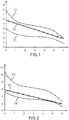
- the Figure 1 represents the force induced by the solenoid and the force of the spring, in accordance with the stroke of both the solenoid and the spring, at room temperature (20°C), according to the prior art.
- the curve C1 represents the solenoid force at 70% rated voltage and the curve C3 represents the solenoid force at 35% rated voltage.
- the curve C2 represents the spring force.
- the point "0" represents the solenoid pulled and the spring charged and the point "6" represents the solenoid released and the spring discharged.
- the magnet force is higher than the spring force over the whole stroke as long as the control-voltage is 70% of rated voltage or higher. This means that the system stays at a position where the solenoid is pulled and the spring charged. If the control-voltage is at 35% of rated voltage or lower, the spring force is higher than the solenoid force over the complete stroke, which means that the sytem moves to the released, discharged position so that the circuit-breaker is tripped.
- the Figure 2 represents the force induced by the solenoid and the force of the spring, in accordance with the stroke of both the solenoid and the spring, at minimum temperature, for example -40°C, according to the prior art.
- the curve C4 represents the solenoid force at 70% rated voltage and the curve C6 represents the solenoid force at 35% rated voltage.
- the curve C5 represents the spring force.
- the force induced by the solenoid at 35% rated voltage is only slightly lower than the spring force. After a certain stroke, both forces are equal. This means that the system starts to move and, most probably, stops at stroke 5 and the circuit-breaker is not tripped. Otherwise, as long as the control-voltage is 70% of rated voltage or higher, the magnet force is higher than the spring force over the whole stroke so that the system stays at a position where the solenoid is pulled and the spring charged.
- the Figure 3 represents the force induced by the solenoid and the force of the spring, in accordance with the stroke of both the solenoid and the spring, at maximum temperature, for example +50°C, according to the prior art.
- the curve C7 represents the solenoid force at 70% of rated voltage and the curve C8 represents the solenoid force at 35% of rated voltage.
- the curve C9 represents the spring force. Even at 70% of rated voltage, the force induced by the solenoid is partially lower that the spring force. This means that the circuit-breaker could trip even at 70% of rated voltage.
- the Figure 4 represents the force induced by the solenoid at 85% of rated voltage (curve C10) and the force of the spring (curve C11), in accordance with the stroke of both the solenoid and the spring, at maximum temperature, for example +50°C, according to the prior art.
- This diagram shows the problem of recharging the spring at 85% of the rated voltage. At 85% of the rated voltage, it must be possible to close the circuit-breaker which means that the solenoid must be able to move the spring from its discharged to its charged position. The solenoid force is partially higher or equal to the spring force. The solenoid cannot charge the spring completely so that the closing of the circuit-breaker is not possible.
- the invention does not have such drawbacks.
- the invention relates to an undervoltage release circuit comprising a solenoid and a spring, the solenoid acting against the spring and being connected to a trip-latch which trips a circuit-breaker as soon as a control voltage drops under a voltage level, characterized in that it comprises a voltage determining device and a switching element controlled by a command signal, the switching element being connected in series with the solenoid, the voltage determining device comprising means for measuring the control-voltage and means for generating a signal according to the control voltage measured, the signal generated according to the control voltage measured constituting the command signal so that the switching element is closed when the control voltage measured is equal or higher than the voltage level and opened as soon as the control voltage is less than the voltage level.
- the voltage determining device comprises a diode in series with a first resistor and a second resistor and the switching element is made of a transistor, the diode having an anode and a cathode, the first resistor having a first terminal and a second terminal, the second resistor having a first terminal and a second terminal and the transitor having a gate, a drain and a source, the first terminal of the first resistor being connected to the anode of the diode and to the gate of the transistor, the second terminal of the first resistor being connected to the second terminal of the undervoltage release circuit and to the drain of the transistor, the first terminal of the second resistor being connected to the first terminal of the undervoltage release circuit and to a first terminal of the solenoid, the second terminal of the second resistor being connected to the cathode of the diode, the source of the transistor being connected to a second terminal of the solenoid.
- the invention also relates to an operating mechanism for tripping a voltage circuit-breaker, the operating mechanism comprising an undervoltage release circuit to trip the circuit-breaker if a control voltage drops under a voltage level, characterized in that the undervoltage release circuit is as circuit according to the invention.
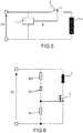
- the Figure 5 represents a diagram of an undervoltage-release circuit of operating-mechanism for circuit-breaker according to the invention.
- the undervoltage-release circuit comprises a voltage determining device 1, a switch 2, a solenoid 3 and a spring.
- the spring is not represented in Figure 5 because the representation of the spring is not useful for the understanding of the invention.
- the switch 2 is in series with the solenoid 3 and the voltage determining device 1 is in parallel with the set constituted by the switch 2 in series with the solenoid 3.
- the control-voltage VC is applied between the terminals of the voltage determining device 1.
- the voltage determining device 1 measures the control voltage VC and outputs a signal K which a function of the control voltage measured.
- the signal K constitutes the command signal of the switch 2.
- the signal K commands the switch 2 in its closed position and a current flows through the solenoid 3.
- the spring (not represented) stays in the charged position.
- the signal K commands the switch 2 so that the switch 2 is put in its opened position. There is no more current in the solenoid 3. Therefore, the solenoid 3 cannot keep the spring in the charged position and the circuit-breaker is tripped.
- the only condition to realise is to choose a solenoid big enough so that its magnetic force is big enough too.
- this condition is very easy to realise with standard solenoids (solenoids bought in the market).
- the Figure 6 represents an example of the undervoltage-release circuit of operating-mechanism for circuit-breaker represented in Figure 5 .
- the voltage determining device 1 is made of a Zener diode D1 and two resistors R1 and R2 in series with the Zener diode.
- the switch 2 is made of a field effect transistor T, for example a power MOSFET.
- the resistor R1 has a first terminal connected to the anode of the Zener diode D1 and to the gate of the field effect transistor T, the second terminal of the resistor R1 being connected to the source of the field effect transistor T.
- the second resistor R2 has a first terminal connected to a first terminal of the solenoid 3, the second terminal of which is connected to the drain of the field effect transistor T.
- the second terminal of the resistor R2 is connected to the cathode of the Zener diode D1.
- the control-voltage VC is applied between the first terminal of the resistor R2 and the second terminal of the resistor R1.
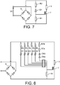
- the figure 7 represents an improvement of the undervoltage-release circuit represented in Figure 5 .
- the circuit represented in Figure 7 comprises a rectifier B placed at the input of the undervoltage release circuit.
- This rectifier makes advantageously the circuit independent of polarity and suitable for active current AC and direct current DC.
- the figure 8 represents an example of undervoltage-release circuit of operating-mechanism which uses a plurality of undervoltage-release circuits as the one shown in Figure 7 .
- the voltage determining device of Figure 8 comprises a 6 way switching controller 4 having one input and six outputs and six branches comprising each at least one Zener diode in series with at least one resistor.
- Each branch is palced between a different output of the 6 way switching controller and the first terminal of the solenoid.
- the 6 way controller 4 allows to connect the gate of the transistor T to anyone of the six branches.
- the voltage determining device comprises a 6 way switching controller and six branches. More generally, the voltage determining device of the undervoltage-release circuit of the invention comprises a N way switching controller and N branches.
Landscapes
- Engineering & Computer Science (AREA)
- Power Engineering (AREA)
- Emergency Protection Circuit Devices (AREA)
- Breakers (AREA)
Claims (5)
- Unterspannungsauslöseschaltkreis aufweisend eine Spule (3), eine Feder, eine Spannungsbestimmungseinrichtung (1) und ein Schaltelement (2), wobei die Spannungsbestimmungseinrichtung (1) ein Mittel zum Messen der Steuerspannung und ein Mittel zur Erzeugung eines Signals (K) entsprechend der gemessenen Steuerspannung aufweist, wobei die Spule (3) gegen die Feder wirkt und mit einem Auslösemechanismus verbunden ist, der einen Trennschalter auslöst, sobald eine Steuerspannung unter ein Spannungsniveau sinkt, dadurch gekennzeichnet, dass das Schaltelement (2) durch ein Steuersignal gesteuert ist, das Schaltelement (2) in Reihe mit der Spule (3) geschaltet ist, das Signal (K) entsprechend der gemessenen Steuerspannung das Steuersignal (K) bildet, so dass das Schaltelement (2) geschlossen wird, wenn die gemessene Steuerspannung gleich groß ist wie oder größer ist als das Spannungsniveau, und geöffnet wird, sobald die Steuerspannung geringer ist als das Spannungsniveau.
- Unterspannungsauslöseschaltkreis nach Anspruch 1, wobei das Spannungsniveau zwischen 40% und 60% der Steuerspannung ist.
- Unterspannungsauslöseschaltkreis nach Anspruch 1 oder 2, wobei die Spannungsbestimmungseinrichtung (1) eine Diode (D1) in Reihe mit einem ersten Widerstand (R1) und einem zweiten Widerstand (R2) aufweist und das Schaltelement (2) durch einen Transistor (T) gebildet ist, wobei die Diode eine Anode und eine Kathode aufweist, wobei der erste Widerstand (R1) einen ersten Anschluss und einen zweiten Anschluss aufweist, wobei der zweite Widerstand (R2) einen ersten Anschluss und einen zweiten Anschluss aufweist und der Transistor (2) einen Steueranschluss, einen Senkenanschluss und einen Quellenanschluss aufweist, wobei der erste Anschluss des ersten Widerstands (R1) mit der Anode der Diode (D1) und mit dem Steueranschluss des Transistors (2) verbunden ist, wobei der zweite Anschluss des ersten Widerstands mit dem zweiten Anschluss des Unterspannungsauslöseschaltkreises und mit dem Senkenanschluss des Transistors verbunden ist, wobei der erste Anschluss des zweiten Widerstands (R2) mit dem ersten Anschluss des Unterspannungsauslöseschaltkreises und mit einem ersten Anschluss der Spule (3) verbunden ist, wobei der zweite Anschluss des zweiten Widerstands (R2) mit der Kathode der Diode (D1) verbunden ist, wobei der Quellenanschluss des Transistors mit einem zweiten Anschluss der Spule (3) verbunden ist.
- Unterspannungsauslöseschaltkreis nach Anspruch 1 oder 2, wobei die Spannungsbestimmungseinrichtung (1) N Zweige aufweist, jeweils aufweisend wenigstens eine Diode (D1, D2, D3, D4, D5, D6a, D6b) in Reihe mit wenigstens einem Widerstand (R2, R3, R4, R5, R6, R7a, R7b), wobei N eine ganze Zahl gleich oder größer als 2 ist, und eine N-Weg-Schaltsteuerung (4), die einen Eingang und N-Ausgänge aufweist, wobei das Schaltelement (2) von einem Transistor mit einem Steueranschluss, einem Senkenanschluss und einem Quellenanschluss gebildet ist, wobei jeder Zweig einen ersten Anschluss aufweist, der die Anode der Diode ist und einen zweiten Anschluss aufweist, der ein Anschluss eines zweiten Widerstands ist, wobei der Eingang der N-Weg-Schaltsteuerung (4) mit dem ersten Anschluss des ersten Widerstands verbunden ist und jeder Ausgang der N Ausgänge mit dem ersten Anschluss eines anderen Zweigs verbunden ist, wobei die zweiten Anschlüsse der N Zweige miteinander zu einem ersten Anschluss des Unterspannungsauslöseschaltkreises und mit einem ersten Anschluss der Spule (3) verbunden sind, wobei der Eingangsanschluss der N-Weg-Schaltsteuerung (4) mit dem Steueranschluss des Transistors und mit einem ersten Anschluss eines zweiten Widerstands verbunden ist, wobei dessen zweiter Anschluss mit einem zweiten Anschluss des Unterspannungsauslöseschaltkreises und mit dem Quellenanschluss des Transistors verbunden ist, wobei dessen Senkenanschluss mit einem zweiten Anschluss der Spule verbunden ist.
- Betriebsmechanismus zum Auslösen eines Spannungsschaltkreistrennschalters, wobei der Betriebsmechanismus einen Unterspannungsauslöseschaltkreis zum Auslösen des Trennschalters aufweist, wenn eine Steuerspannung unter ein Spannungsniveau sinkt, dadurch gekennzeichnet, dass der Unterspannungsauslöseschaltkreis ein Schaltkreis nach irgendeinem der Ansprüche 1-4 ist.
Priority Applications (6)
| Application Number | Priority Date | Filing Date | Title |
|---|---|---|---|
| EP15153343.7A EP3051644B1 (de) | 2015-01-30 | 2015-01-30 | Unterspannungsauslöseschaltung eines Betriebsmechanismus zum Auslösen eines Spannungsschutzschalters |
| CN201680007865.8A CN107210161B (zh) | 2015-01-30 | 2016-01-28 | 用于使电压断路器跳闸的操作机构的欠电压释放电路 |
| PCT/EP2016/051766 WO2016120367A1 (en) | 2015-01-30 | 2016-01-28 | Undervoltage-release circuit of operating-mechanism for tripping a voltage circuit-breaker |
| US15/547,098 US20180138692A1 (en) | 2015-01-30 | 2016-01-28 | Undervoltage-release circuit of operating-mechanism for tripping a voltage circuit-breaker |
| CA2974557A CA2974557A1 (en) | 2015-01-30 | 2016-01-28 | Undervoltage-release circuit of operating-mechanism for tripping a voltage circuit-breaker |
| BR112017016187-7A BR112017016187A2 (pt) | 2015-01-30 | 2016-01-28 | ?circuito de liberação de subtensão e mecanismo operacional para disparar um disjuntor de tensão? |
Applications Claiming Priority (1)
| Application Number | Priority Date | Filing Date | Title |
|---|---|---|---|
| EP15153343.7A EP3051644B1 (de) | 2015-01-30 | 2015-01-30 | Unterspannungsauslöseschaltung eines Betriebsmechanismus zum Auslösen eines Spannungsschutzschalters |
Publications (2)
| Publication Number | Publication Date |
|---|---|
| EP3051644A1 EP3051644A1 (de) | 2016-08-03 |
| EP3051644B1 true EP3051644B1 (de) | 2019-10-02 |
Family
ID=52432735
Family Applications (1)
| Application Number | Title | Priority Date | Filing Date |
|---|---|---|---|
| EP15153343.7A Active EP3051644B1 (de) | 2015-01-30 | 2015-01-30 | Unterspannungsauslöseschaltung eines Betriebsmechanismus zum Auslösen eines Spannungsschutzschalters |
Country Status (6)
| Country | Link |
|---|---|
| US (1) | US20180138692A1 (de) |
| EP (1) | EP3051644B1 (de) |
| CN (1) | CN107210161B (de) |
| BR (1) | BR112017016187A2 (de) |
| CA (1) | CA2974557A1 (de) |
| WO (1) | WO2016120367A1 (de) |
Families Citing this family (2)
| Publication number | Priority date | Publication date | Assignee | Title |
|---|---|---|---|---|
| DE102015119512A1 (de) * | 2015-11-12 | 2017-05-18 | Eaton Electrical Ip Gmbh & Co. Kg | Verfahren und Vorrichtung zur Steuerung eines elektromagnetischen Antriebs eines Schaltgeräts |
| US10950167B1 (en) * | 2019-10-17 | 2021-03-16 | Solomon Systech (Shenzhen) Limited | LED display with electroluminescent components |
Family Cites Families (11)
| Publication number | Priority date | Publication date | Assignee | Title |
|---|---|---|---|---|
| US2033177A (en) * | 1928-05-05 | 1936-03-10 | Simplex Valve & Meter Company | Recording mechanism |
| US2033171A (en) * | 1934-04-23 | 1936-03-10 | Minnie E Sharp | Brake shoe key |
| GB2033177B (en) * | 1978-09-20 | 1982-10-13 | Dorman Smith Switchgear Ltd | Circuit breaker with undervoltage release |
| US4331996A (en) * | 1979-08-22 | 1982-05-25 | Westinghouse Electric Corp. | Time delayed undervoltage relay |
| US4352138A (en) * | 1980-11-25 | 1982-09-28 | Mcgraw-Edison Company | Backup trip circuit for a circuit breaker |
| US7355301B2 (en) * | 2003-02-26 | 2008-04-08 | Cannon Technologies, Inc. | Load control receiver with line under voltage and line under frequency detection and load shedding |
| US20050243491A1 (en) * | 2004-04-28 | 2005-11-03 | James Tanis | Multi-function power monitor and circuit protector |
| DE102010054402A1 (de) * | 2010-12-14 | 2012-06-14 | Init Innovative Informatikanwendungen In Transport-, Verkehrs- Und Leitsystemen Gmbh | Schaltung zum Schutz eines elektrischen Verbrauchers gegen Überspannungen |
| CN102780203A (zh) * | 2012-07-31 | 2012-11-14 | 德力西电气有限公司 | 一种过欠压保护电路 |
| CN202817699U (zh) * | 2012-08-06 | 2013-03-20 | 上海诺雅克电气有限公司 | 一种直流欠压脱扣器和断路器 |
| JP2014199724A (ja) * | 2013-03-29 | 2014-10-23 | パナソニック株式会社 | 回路遮断器の不足電圧引き外し装置及び過電圧・不足電圧引き外し装置 |
-
2015
- 2015-01-30 EP EP15153343.7A patent/EP3051644B1/de active Active
-
2016
- 2016-01-28 BR BR112017016187-7A patent/BR112017016187A2/pt not_active Application Discontinuation
- 2016-01-28 US US15/547,098 patent/US20180138692A1/en not_active Abandoned
- 2016-01-28 CA CA2974557A patent/CA2974557A1/en not_active Abandoned
- 2016-01-28 WO PCT/EP2016/051766 patent/WO2016120367A1/en not_active Ceased
- 2016-01-28 CN CN201680007865.8A patent/CN107210161B/zh active Active
Non-Patent Citations (1)
| Title |
|---|
| None * |
Also Published As
| Publication number | Publication date |
|---|---|
| WO2016120367A1 (en) | 2016-08-04 |
| BR112017016187A2 (pt) | 2018-04-17 |
| CN107210161B (zh) | 2020-06-09 |
| CA2974557A1 (en) | 2016-08-04 |
| CN107210161A (zh) | 2017-09-26 |
| US20180138692A1 (en) | 2018-05-17 |
| EP3051644A1 (de) | 2016-08-03 |
Similar Documents
| Publication | Publication Date | Title |
|---|---|---|
| US10811867B2 (en) | Hybrid air-gap / solid-state circuit breaker | |
| CN107004526B (zh) | 保护开关及其运行方法 | |
| EP1294069A1 (de) | Elektronischer Schutzschalter | |
| EP2579291A1 (de) | Spulenaktuator für eine Schaltvorrichtung und zugehörige Schaltvorrichtung | |
| US20080157776A1 (en) | Measurement of analog coil voltage and coil current | |
| US9577419B2 (en) | Shunt trip control circuits using shunt trip signal accumulator and methods of operating the same | |
| EP3051644B1 (de) | Unterspannungsauslöseschaltung eines Betriebsmechanismus zum Auslösen eines Spannungsschutzschalters | |
| US6242845B1 (en) | Electronic driving circuit for a bistable actuator | |
| CN102354943B (zh) | 一种电子脱扣器的工作方法 | |
| EP3234977B1 (de) | Schaltungsunterbrechungsvorrichtung mit automatischem reduziertem lichtbogenmodus und verfahren zum betrieb davon | |
| US6788515B1 (en) | Over-current control | |
| US3735215A (en) | Self-powered relay target circuit | |
| US1250746A (en) | Time-limit tripping mechanism. | |
| EP2693456B1 (de) | Spulenaktuator für eine Schaltvorrichtung und zugehöriges Korrekturverfahren | |
| US8605405B2 (en) | Method and circuit for increasing the speed of electromechanical output on a protective relay | |
| RU2333584C1 (ru) | Устройство токовой защиты с зависимой выдержкой времени на герконах | |
| US10056833B2 (en) | Voltage regulator for inductive loads | |
| DE102004046810A1 (de) | Elektronischer Schutzschalter mit einstellbarer Auslösecharakteristik | |
| JPH1167021A (ja) | 遮断器の遮断電流カウンタ装置 | |
| US5991144A (en) | Circuit for tripping breaker | |
| HK40035799A (en) | Hybrid air-gap/solid-state circuit breaker | |
| WO2012042318A1 (en) | Powerless reset in a self powered relay | |
| CN104054152B (zh) | 用于增加机电式保护继电器的速度的方法及电路 | |
| JPS6130912A (ja) | 回路遮断器 |
Legal Events
| Date | Code | Title | Description |
|---|---|---|---|
| PUAI | Public reference made under article 153(3) epc to a published international application that has entered the european phase |
Free format text: ORIGINAL CODE: 0009012 |
|
| AK | Designated contracting states |
Kind code of ref document: A1 Designated state(s): AL AT BE BG CH CY CZ DE DK EE ES FI FR GB GR HR HU IE IS IT LI LT LU LV MC MK MT NL NO PL PT RO RS SE SI SK SM TR |
|
| AX | Request for extension of the european patent |
Extension state: BA ME |
|
| STAA | Information on the status of an ep patent application or granted ep patent |
Free format text: STATUS: REQUEST FOR EXAMINATION WAS MADE |
|
| 17P | Request for examination filed |
Effective date: 20161216 |
|
| RBV | Designated contracting states (corrected) |
Designated state(s): AL AT BE BG CH CY CZ DE DK EE ES FI FR GB GR HR HU IE IS IT LI LT LU LV MC MK MT NL NO PL PT RO RS SE SI SK SM TR |
|
| STAA | Information on the status of an ep patent application or granted ep patent |
Free format text: STATUS: EXAMINATION IS IN PROGRESS |
|
| 17Q | First examination report despatched |
Effective date: 20181105 |
|
| GRAP | Despatch of communication of intention to grant a patent |
Free format text: ORIGINAL CODE: EPIDOSNIGR1 |
|
| STAA | Information on the status of an ep patent application or granted ep patent |
Free format text: STATUS: GRANT OF PATENT IS INTENDED |
|
| INTG | Intention to grant announced |
Effective date: 20190528 |
|
| GRAS | Grant fee paid |
Free format text: ORIGINAL CODE: EPIDOSNIGR3 |
|
| GRAA | (expected) grant |
Free format text: ORIGINAL CODE: 0009210 |
|
| STAA | Information on the status of an ep patent application or granted ep patent |
Free format text: STATUS: THE PATENT HAS BEEN GRANTED |
|
| AK | Designated contracting states |
Kind code of ref document: B1 Designated state(s): AL AT BE BG CH CY CZ DE DK EE ES FI FR GB GR HR HU IE IS IT LI LT LU LV MC MK MT NL NO PL PT RO RS SE SI SK SM TR |
|
| REG | Reference to a national code |
Ref country code: GB Ref legal event code: FG4D |
|
| REG | Reference to a national code |
Ref country code: CH Ref legal event code: EP Ref country code: CH Ref legal event code: NV Representative=s name: VALIPAT S.A. C/O BOVARD SA NEUCHATEL, CH Ref country code: AT Ref legal event code: REF Ref document number: 1187261 Country of ref document: AT Kind code of ref document: T Effective date: 20191015 |
|
| REG | Reference to a national code |
Ref country code: DE Ref legal event code: R096 Ref document number: 602015038916 Country of ref document: DE |
|
| REG | Reference to a national code |
Ref country code: IE Ref legal event code: FG4D |
|
| REG | Reference to a national code |
Ref country code: NL Ref legal event code: MP Effective date: 20191002 |
|
| REG | Reference to a national code |
Ref country code: LT Ref legal event code: MG4D |
|
| REG | Reference to a national code |
Ref country code: AT Ref legal event code: MK05 Ref document number: 1187261 Country of ref document: AT Kind code of ref document: T Effective date: 20191002 |
|
| PG25 | Lapsed in a contracting state [announced via postgrant information from national office to epo] |
Ref country code: PT Free format text: LAPSE BECAUSE OF FAILURE TO SUBMIT A TRANSLATION OF THE DESCRIPTION OR TO PAY THE FEE WITHIN THE PRESCRIBED TIME-LIMIT Effective date: 20200203 Ref country code: BG Free format text: LAPSE BECAUSE OF FAILURE TO SUBMIT A TRANSLATION OF THE DESCRIPTION OR TO PAY THE FEE WITHIN THE PRESCRIBED TIME-LIMIT Effective date: 20200102 Ref country code: FI Free format text: LAPSE BECAUSE OF FAILURE TO SUBMIT A TRANSLATION OF THE DESCRIPTION OR TO PAY THE FEE WITHIN THE PRESCRIBED TIME-LIMIT Effective date: 20191002 Ref country code: AT Free format text: LAPSE BECAUSE OF FAILURE TO SUBMIT A TRANSLATION OF THE DESCRIPTION OR TO PAY THE FEE WITHIN THE PRESCRIBED TIME-LIMIT Effective date: 20191002 Ref country code: LV Free format text: LAPSE BECAUSE OF FAILURE TO SUBMIT A TRANSLATION OF THE DESCRIPTION OR TO PAY THE FEE WITHIN THE PRESCRIBED TIME-LIMIT Effective date: 20191002 Ref country code: SE Free format text: LAPSE BECAUSE OF FAILURE TO SUBMIT A TRANSLATION OF THE DESCRIPTION OR TO PAY THE FEE WITHIN THE PRESCRIBED TIME-LIMIT Effective date: 20191002 Ref country code: ES Free format text: LAPSE BECAUSE OF FAILURE TO SUBMIT A TRANSLATION OF THE DESCRIPTION OR TO PAY THE FEE WITHIN THE PRESCRIBED TIME-LIMIT Effective date: 20191002 Ref country code: NL Free format text: LAPSE BECAUSE OF FAILURE TO SUBMIT A TRANSLATION OF THE DESCRIPTION OR TO PAY THE FEE WITHIN THE PRESCRIBED TIME-LIMIT Effective date: 20191002 Ref country code: GR Free format text: LAPSE BECAUSE OF FAILURE TO SUBMIT A TRANSLATION OF THE DESCRIPTION OR TO PAY THE FEE WITHIN THE PRESCRIBED TIME-LIMIT Effective date: 20200103 Ref country code: LT Free format text: LAPSE BECAUSE OF FAILURE TO SUBMIT A TRANSLATION OF THE DESCRIPTION OR TO PAY THE FEE WITHIN THE PRESCRIBED TIME-LIMIT Effective date: 20191002 Ref country code: NO Free format text: LAPSE BECAUSE OF FAILURE TO SUBMIT A TRANSLATION OF THE DESCRIPTION OR TO PAY THE FEE WITHIN THE PRESCRIBED TIME-LIMIT Effective date: 20200102 Ref country code: PL Free format text: LAPSE BECAUSE OF FAILURE TO SUBMIT A TRANSLATION OF THE DESCRIPTION OR TO PAY THE FEE WITHIN THE PRESCRIBED TIME-LIMIT Effective date: 20191002 |
|
| PG25 | Lapsed in a contracting state [announced via postgrant information from national office to epo] |
Ref country code: CZ Free format text: LAPSE BECAUSE OF FAILURE TO SUBMIT A TRANSLATION OF THE DESCRIPTION OR TO PAY THE FEE WITHIN THE PRESCRIBED TIME-LIMIT Effective date: 20191002 Ref country code: HR Free format text: LAPSE BECAUSE OF FAILURE TO SUBMIT A TRANSLATION OF THE DESCRIPTION OR TO PAY THE FEE WITHIN THE PRESCRIBED TIME-LIMIT Effective date: 20191002 Ref country code: RS Free format text: LAPSE BECAUSE OF FAILURE TO SUBMIT A TRANSLATION OF THE DESCRIPTION OR TO PAY THE FEE WITHIN THE PRESCRIBED TIME-LIMIT Effective date: 20191002 Ref country code: IS Free format text: LAPSE BECAUSE OF FAILURE TO SUBMIT A TRANSLATION OF THE DESCRIPTION OR TO PAY THE FEE WITHIN THE PRESCRIBED TIME-LIMIT Effective date: 20200224 |
|
| PG25 | Lapsed in a contracting state [announced via postgrant information from national office to epo] |
Ref country code: AL Free format text: LAPSE BECAUSE OF FAILURE TO SUBMIT A TRANSLATION OF THE DESCRIPTION OR TO PAY THE FEE WITHIN THE PRESCRIBED TIME-LIMIT Effective date: 20191002 |
|
| REG | Reference to a national code |
Ref country code: DE Ref legal event code: R097 Ref document number: 602015038916 Country of ref document: DE |
|
| PG2D | Information on lapse in contracting state deleted |
Ref country code: IS |
|
| PG25 | Lapsed in a contracting state [announced via postgrant information from national office to epo] |
Ref country code: RO Free format text: LAPSE BECAUSE OF FAILURE TO SUBMIT A TRANSLATION OF THE DESCRIPTION OR TO PAY THE FEE WITHIN THE PRESCRIBED TIME-LIMIT Effective date: 20191002 Ref country code: EE Free format text: LAPSE BECAUSE OF FAILURE TO SUBMIT A TRANSLATION OF THE DESCRIPTION OR TO PAY THE FEE WITHIN THE PRESCRIBED TIME-LIMIT Effective date: 20191002 Ref country code: DK Free format text: LAPSE BECAUSE OF FAILURE TO SUBMIT A TRANSLATION OF THE DESCRIPTION OR TO PAY THE FEE WITHIN THE PRESCRIBED TIME-LIMIT Effective date: 20191002 Ref country code: IS Free format text: LAPSE BECAUSE OF FAILURE TO SUBMIT A TRANSLATION OF THE DESCRIPTION OR TO PAY THE FEE WITHIN THE PRESCRIBED TIME-LIMIT Effective date: 20200202 |
|
| PLBE | No opposition filed within time limit |
Free format text: ORIGINAL CODE: 0009261 |
|
| STAA | Information on the status of an ep patent application or granted ep patent |
Free format text: STATUS: NO OPPOSITION FILED WITHIN TIME LIMIT |
|
| PG25 | Lapsed in a contracting state [announced via postgrant information from national office to epo] |
Ref country code: MC Free format text: LAPSE BECAUSE OF FAILURE TO SUBMIT A TRANSLATION OF THE DESCRIPTION OR TO PAY THE FEE WITHIN THE PRESCRIBED TIME-LIMIT Effective date: 20191002 Ref country code: SK Free format text: LAPSE BECAUSE OF FAILURE TO SUBMIT A TRANSLATION OF THE DESCRIPTION OR TO PAY THE FEE WITHIN THE PRESCRIBED TIME-LIMIT Effective date: 20191002 Ref country code: IT Free format text: LAPSE BECAUSE OF FAILURE TO SUBMIT A TRANSLATION OF THE DESCRIPTION OR TO PAY THE FEE WITHIN THE PRESCRIBED TIME-LIMIT Effective date: 20191002 Ref country code: SM Free format text: LAPSE BECAUSE OF FAILURE TO SUBMIT A TRANSLATION OF THE DESCRIPTION OR TO PAY THE FEE WITHIN THE PRESCRIBED TIME-LIMIT Effective date: 20191002 |
|
| 26N | No opposition filed |
Effective date: 20200703 |
|
| REG | Reference to a national code |
Ref country code: BE Ref legal event code: MM Effective date: 20200131 |
|
| PG25 | Lapsed in a contracting state [announced via postgrant information from national office to epo] |
Ref country code: LU Free format text: LAPSE BECAUSE OF NON-PAYMENT OF DUE FEES Effective date: 20200130 |
|
| PG25 | Lapsed in a contracting state [announced via postgrant information from national office to epo] |
Ref country code: SI Free format text: LAPSE BECAUSE OF FAILURE TO SUBMIT A TRANSLATION OF THE DESCRIPTION OR TO PAY THE FEE WITHIN THE PRESCRIBED TIME-LIMIT Effective date: 20191002 Ref country code: BE Free format text: LAPSE BECAUSE OF NON-PAYMENT OF DUE FEES Effective date: 20200131 |
|
| PG25 | Lapsed in a contracting state [announced via postgrant information from national office to epo] |
Ref country code: IE Free format text: LAPSE BECAUSE OF NON-PAYMENT OF DUE FEES Effective date: 20200130 |
|
| PG25 | Lapsed in a contracting state [announced via postgrant information from national office to epo] |
Ref country code: TR Free format text: LAPSE BECAUSE OF FAILURE TO SUBMIT A TRANSLATION OF THE DESCRIPTION OR TO PAY THE FEE WITHIN THE PRESCRIBED TIME-LIMIT Effective date: 20191002 Ref country code: MT Free format text: LAPSE BECAUSE OF FAILURE TO SUBMIT A TRANSLATION OF THE DESCRIPTION OR TO PAY THE FEE WITHIN THE PRESCRIBED TIME-LIMIT Effective date: 20191002 Ref country code: CY Free format text: LAPSE BECAUSE OF FAILURE TO SUBMIT A TRANSLATION OF THE DESCRIPTION OR TO PAY THE FEE WITHIN THE PRESCRIBED TIME-LIMIT Effective date: 20191002 |
|
| PG25 | Lapsed in a contracting state [announced via postgrant information from national office to epo] |
Ref country code: MK Free format text: LAPSE BECAUSE OF FAILURE TO SUBMIT A TRANSLATION OF THE DESCRIPTION OR TO PAY THE FEE WITHIN THE PRESCRIBED TIME-LIMIT Effective date: 20191002 |
|
| P01 | Opt-out of the competence of the unified patent court (upc) registered |
Effective date: 20230522 |
|
| PGFP | Annual fee paid to national office [announced via postgrant information from national office to epo] |
Ref country code: GB Payment date: 20251220 Year of fee payment: 12 |
|
| PGFP | Annual fee paid to national office [announced via postgrant information from national office to epo] |
Ref country code: FR Payment date: 20251217 Year of fee payment: 12 |
|
| REG | Reference to a national code |
Ref country code: CH Ref legal event code: U11 Free format text: ST27 STATUS EVENT CODE: U-0-0-U10-U11 (AS PROVIDED BY THE NATIONAL OFFICE) Effective date: 20260201 |
|
| PGFP | Annual fee paid to national office [announced via postgrant information from national office to epo] |
Ref country code: DE Payment date: 20251217 Year of fee payment: 12 |
|
| PGFP | Annual fee paid to national office [announced via postgrant information from national office to epo] |
Ref country code: CH Payment date: 20260201 Year of fee payment: 12 |