EP3051644A1 - Undervoltage-release circuit of operating-mechanism for tripping a voltage circuit-breaker - Google Patents
Undervoltage-release circuit of operating-mechanism for tripping a voltage circuit-breaker Download PDFInfo
- Publication number
- EP3051644A1 EP3051644A1 EP15153343.7A EP15153343A EP3051644A1 EP 3051644 A1 EP3051644 A1 EP 3051644A1 EP 15153343 A EP15153343 A EP 15153343A EP 3051644 A1 EP3051644 A1 EP 3051644A1
- Authority
- EP
- European Patent Office
- Prior art keywords
- terminal
- voltage
- solenoid
- resistor
- circuit
- Prior art date
- Legal status (The legal status is an assumption and is not a legal conclusion. Google has not performed a legal analysis and makes no representation as to the accuracy of the status listed.)
- Granted
Links
Images

Classifications
-
- H—ELECTRICITY
- H02—GENERATION; CONVERSION OR DISTRIBUTION OF ELECTRIC POWER
- H02H—EMERGENCY PROTECTIVE CIRCUIT ARRANGEMENTS
- H02H3/00—Emergency protective circuit arrangements for automatic disconnection directly responsive to an undesired change from normal electric working condition with or without subsequent reconnection ; integrated protection
- H02H3/24—Emergency protective circuit arrangements for automatic disconnection directly responsive to an undesired change from normal electric working condition with or without subsequent reconnection ; integrated protection responsive to undervoltage or no-voltage
-
- H—ELECTRICITY
- H01—ELECTRIC ELEMENTS
- H01H—ELECTRIC SWITCHES; RELAYS; SELECTORS; EMERGENCY PROTECTIVE DEVICES
- H01H47/00—Circuit arrangements not adapted to a particular application of the relay and designed to obtain desired operating characteristics or to provide energising current
- H01H47/22—Circuit arrangements not adapted to a particular application of the relay and designed to obtain desired operating characteristics or to provide energising current for supplying energising current for relay coil
- H01H47/32—Energising current supplied by semiconductor device
- H01H47/325—Energising current supplied by semiconductor device by switching regulator
-
- H—ELECTRICITY
- H01—ELECTRIC ELEMENTS
- H01H—ELECTRIC SWITCHES; RELAYS; SELECTORS; EMERGENCY PROTECTIVE DEVICES
- H01H83/00—Protective switches, e.g. circuit-breaking switches, or protective relays operated by abnormal electrical conditions otherwise than solely by excess current
- H01H83/12—Protective switches, e.g. circuit-breaking switches, or protective relays operated by abnormal electrical conditions otherwise than solely by excess current operated by voltage falling below a predetermined value, e.g. for no-volt protection
Definitions
- the invention relates to an undervoltage release circuit of an operating mechanism for tripping a voltage circuit breaker and to an operating-mechanism for tripping a voltage circuit-breaker which comprises an undervoltage release circuit according to the invention.
- the energy to trip a circuit-breaker is stored in a spring (spring-operated mechanism) or in a hydraulic tank (hydraulic-operated mechanism).
- the spring is held in its charged position using a latching-system, while the hydraulic tank is kept under pressure by a closed valve.
- the latching-system or the valve is opened either manually or by an electromagnetic solenoid (coil).
- control-voltage is the power-supply with which the substation which contains the circuit-breaker is controlled (all mechanisms, protection relays, position indicators, etc. are activated by the control-voltage).
- linear solenoids are used to realize the undervoltage-release function.
- the solenoid acts against a spring and is connected to a trip-latch. As long as the control-voltage is high enough, the solenoid holds the spring in charged position. When the control-voltage drops, the magnetic force of the solenoid gets weaker so it cannot hold the spring in its charged position. Thus, the spring discharges and trips the circuit-breeaker.
- the main problem of such an electromagnetic system is to find the balance between the magnetic force induced by the solenoid and the force of the spring, especially when working under low or high temperatures. Due to the temperature-coefficient of the copper-windings of the solenoid, the magnetic force induced by the solenoid is depending on the temperature. Another problem is that the force induced by the solenoid is a very non linear force, while the force of the spring is a linear force.
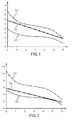
- the Figure 1 represents the force induced by the solenoid and the force of the spring, in accordance with the stroke of both the solenoid and the spring, at room temperature (20°C), according to the prior art.
- the curve C1 represents the solenoid force at 70% rated voltage and the curve C3 represents the solenoid force at 35% rated voltage.
- the curve C2 represents the spring force.
- the point "0" represents the solenoid pulled and the spring charged and the point "6" represents the solenoid released and the spring discharged.
- the magnet force is higher than the spring force over the whole stroke as long as the control-voltage is 70% of rated voltage or higher. This means that the system stays at a position where the solenoid is pulled and the spring charged. If the control-voltage is at 35% of rated voltage or lower, the spring force is higher than the solenoid force over the complete stroke, which means that the sytem moves to the released, discharged position so that the circuit-breaker is tripped.
- the Figure 2 represents the force induced by the solenoid and the force of the spring, in accordance with the stroke of both the solenoid and the spring, at minimum temperature, for example -40°C, according to the prior art.
- the curve C4 represents the solenoid force at 70% rated voltage and the curve C6 represents the solenoid force at 35% rated voltage.
- the curve C5 represents the spring force.
- the force induced by the solenoid at 35% rated voltage is only slightly lower than the spring force. After a certain stroke, both forces are equal. This means that the system starts to move and, most probably, stops at stroke 5 and the circuit-breaker is not tripped. Otherwise, as long as the control-voltage is 70% of rated voltage or higher, the magnet force is higher than the spring force over the whole stroke so that the system stays at a position where the solenoid is pulled and the spring charged.
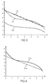
- the Figure 3 represents the force induced by the solenoid and the force of the spring, in accordance with the stroke of both the solenoid and the spring, at maximum temperature, for example +50°C, according to the prior art.
- the curve C7 represents the solenoid force at 70% of rated voltage and the curve C8 represents the solenoid force at 35% of rated voltage.
- the curve C9 represents the spring force. Even at 70% of rated voltage, the force induced by the solenoid is partially lower that the spring force. This means that the circuit-breaker could trip even at 70% of rated voltage.
- the Figure 4 represents the force induced by the solenoid at 85% of rated voltage (curve C10) and the force of the spring (curve C11), in accordance with the stroke of both the solenoid and the spring, at maximum temperature, for example +50°C, according to the prior art.
- This diagram shows the problem of recharging the spring at 85% of the rated voltage. At 85% of the rated voltage, it must be possible to close the circuit-breaker which means that the solenoid must be able to move the spring from its discharged to its charged position. The solenoid force is partially higher or equal to the spring force. The solenoid cannot charge the spring completely so that the closing of the circuit-breaker is not possible.
- the invention does not have such drawbacks.
- the invention relates to an undervoltage release circuit comprising a solenoid and a spring, the solenoid acting against the spring and being connected to a trip-latch which trips a circuit-breaker as soon as a control voltage drops under a voltage level, characterized in that it comprises a voltage determining device and a switching element controlled by a command signal, the switching element being connected in series with the solenoid, the voltage determining device comprising means for measuring the control-voltage and means for generating a signal according to the control voltage measured, the signal generated according to the control voltage measured constituting the command signal so that the switching element is closed when the control voltage measured is equal or higher than the voltage level and opened as soon as the control voltage is less than the voltage level.
- the voltage determining device comprises a diode in series with a first resistor and a second resistor and the switching element is made of a transistor, the diode having an anode and a cathode, the first resistor having a first terminal and a second terminal, the second resistor having a first terminal and a second terminal and the transitor having a gate, a drain and a source, the first terminal of the first resistor being connected to the anode of the diode and to the gate of the transistor, the second terminal of the first resistor being connected to the second terminal of the undervoltage release circuit and to the drain of the transistor, the first terminal of the second resistor being connected to the first terminal of the undervoltage release circuit and to a first terminal of the solenoid, the second terminal of the second resistor being connected to the cathode of the diode, the source of the transistor being connected to a second terminal of the solenoid.
- the invention also relates to an operating mechanism for tripping a voltage circuit-breaker, the operating mechanism comprising an undervoltage release circuit to trip the circuit-breaker if a control voltage drops under a voltage level, characterized in that the undervoltage release circuit is as circuit according to the invention.
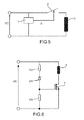
- the Figure 5 represents a diagram of an undervoltage-release circuit of operating-mechanism for circuit-breaker according to the invention.
- the undervoltage-release circuit comprises a voltage determining device 1, a switch 2, a solenoid 3 and a spring.
- the spring is not represented in Figure 5 because the representation of the spring is not useful for the understanding of the invention.
- the switch 2 is in series with the solenoid 3 and the voltage determining device 1 is in parallel with the set constituted by the switch 2 in series with the solenoid 3.
- the control-voltage VC is applied between the terminals of the voltage determining device 1.
- the voltage determining device 1 measures the control voltage VC and outputs a signal K which a function of the control voltage measured.
- the signal K constitutes the command signal of the switch 2.
- the signal K commands the switch 2 in its closed position and a current flows through the solenoid 3.
- the spring (not represented) stays in the charged position.
- the signal K commands the switch 2 so that the switch 2 is put in its opened position. There is no more current in the solenoid 3. Therefore, the solenoid 3 cannot keep the spring in the charged position and the circuit-breaker is tripped.
- the only condition to realise is to choose a solenoid big enough so that its magnetic force is big enough too.
- this condition is very easy to realise with standard solenoids (solenoids bought in the market).
- the Figure 6 represents an example of the undervoltage-release circuit of operating-mechanism for circuit-breaker represented in Figure 5 .
- the voltage determining device 1 is made of a Zener diode D1 and two resistors R1 and R2 in series with the Zener diode.
- the switch 2 is made of a field effect transistor T, for example a power MOSFET.
- the resistor R1 has a first terminal connected to the anode of the Zener diode D1 and to the gate of the field effect transistor T, the second terminal of the resistor R1 being connected to the source of the field effect transistor T.
- the second resistor R2 has a first terminal connected to a first terminal of the solenoid 3, the second terminal of which is connected to the drain of the field effect transistor T.
- the second terminal of the resistor R2 is connected to the cathode of the Zener diode D1.
- the control-voltage VC is applied between the first terminal of the resistor R2 and the second terminal of the resistor R1.
- the figure 7 represents an improvement of the undervoltage-release circuit represented in Figure 5 .
- the circuit represented in Figure 7 comprises a rectifier B placed at the input of the undervoltage release circuit.
- This rectifier makes advantageously the circuit independent of polarity and suitable for active current AC and direct current DC.
- the figure 8 represents an example of undervoltage-release circuit of operating-mechanism which uses a plurality of undervoltage-release circuits as the one shown in Figure 7 .
- the voltage determining device of Figure 8 comprises a 6 way switching controller 4 having one input and six outputs and six branches comprising each at least one Zener diode in series with at least one resistor.
- Each branch is palced between a different output of the 6 way switching controller and the first terminal of the solenoid.
- the 6 way controller 4 allows to connect the gate of the transistor T to anyone of the six branches.
- the voltage determining device comprises a 6 way switching controller and six branches. More generally, the voltage determining device of the undervoltage-release circuit of the invention comprises a N way switching controller and N branches.
Landscapes
- Engineering & Computer Science (AREA)
- Power Engineering (AREA)
- Emergency Protection Circuit Devices (AREA)
- Breakers (AREA)
Abstract
Description
- The invention relates to an undervoltage release circuit of an operating mechanism for tripping a voltage circuit breaker and to an operating-mechanism for tripping a voltage circuit-breaker which comprises an undervoltage release circuit according to the invention.
- The energy to trip a circuit-breaker is stored in a spring (spring-operated mechanism) or in a hydraulic tank (hydraulic-operated mechanism). The spring is held in its charged position using a latching-system, while the hydraulic tank is kept under pressure by a closed valve. To trip the circuit-breaker, the latching-system or the valve is opened either manually or by an electromagnetic solenoid (coil).
- It is sometimes required a special equipment called "undervoltage-release circuit" to trip the circuit-breaker in case the control-voltage drops under a certain voltage level. As known by the man skilled in the art, the "control-voltage" is the power-supply with which the substation which contains the circuit-breaker is controlled (all mechanisms, protection relays, position indicators, etc. are activated by the control-voltage).
- The tripping of the circuit-breaker is then specified as follows:
- The undervoltage-release circuit does not trip the circuit-breaker as long as the control-voltage is higher than 70% of rated voltage;
- The undervoltage-release circuit must trip the circuit-breaker if the control-voltage is lower than 35% the rated voltage.
- Furthermore, a reclosing must be possible as soon as the control-voltage is minimum 85% of rated voltage.
- In some operating-mechanisms of the prior art, linear solenoids are used to realize the undervoltage-release function. The solenoid acts against a spring and is connected to a trip-latch. As long as the control-voltage is high enough, the solenoid holds the spring in charged position. When the control-voltage drops, the magnetic force of the solenoid gets weaker so it cannot hold the spring in its charged position. Thus, the spring discharges and trips the circuit-breeaker.
- The main problem of such an electromagnetic system is to find the balance between the magnetic force induced by the solenoid and the force of the spring, especially when working under low or high temperatures. Due to the temperature-coefficient of the copper-windings of the solenoid, the magnetic force induced by the solenoid is depending on the temperature. Another problem is that the force induced by the solenoid is a very non linear force, while the force of the spring is a linear force.
- The
Figure 1 represents the force induced by the solenoid and the force of the spring, in accordance with the stroke of both the solenoid and the spring, at room temperature (20°C), according to the prior art. - The curve C1 represents the solenoid force at 70% rated voltage and the curve C3 represents the solenoid force at 35% rated voltage. The curve C2 represents the spring force. On the abscissa scale, the point "0" represents the solenoid pulled and the spring charged and the point "6" represents the solenoid released and the spring discharged.
- The magnet force is higher than the spring force over the whole stroke as long as the control-voltage is 70% of rated voltage or higher. This means that the system stays at a position where the solenoid is pulled and the spring charged. If the control-voltage is at 35% of rated voltage or lower, the spring force is higher than the solenoid force over the complete stroke, which means that the sytem moves to the released, discharged position so that the circuit-breaker is tripped.
- The
Figure 2 represents the force induced by the solenoid and the force of the spring, in accordance with the stroke of both the solenoid and the spring, at minimum temperature, for example -40°C, according to the prior art. - The curve C4 represents the solenoid force at 70% rated voltage and the curve C6 represents the solenoid force at 35% rated voltage. The curve C5 represents the spring force. The force induced by the solenoid at 35% rated voltage is only slightly lower than the spring force. After a certain stroke, both forces are equal. This means that the system starts to move and, most probably, stops at
stroke 5 and the circuit-breaker is not tripped. Otherwise, as long as the control-voltage is 70% of rated voltage or higher, the magnet force is higher than the spring force over the whole stroke so that the system stays at a position where the solenoid is pulled and the spring charged. - The
Figure 3 represents the force induced by the solenoid and the force of the spring, in accordance with the stroke of both the solenoid and the spring, at maximum temperature, for example +50°C, according to the prior art. - The curve C7 represents the solenoid force at 70% of rated voltage and the curve C8 represents the solenoid force at 35% of rated voltage. The curve C9 represents the spring force. Even at 70% of rated voltage, the force induced by the solenoid is partially lower that the spring force. This means that the circuit-breaker could trip even at 70% of rated voltage.
- The
Figure 4 represents the force induced by the solenoid at 85% of rated voltage (curve C10) and the force of the spring (curve C11), in accordance with the stroke of both the solenoid and the spring, at maximum temperature, for example +50°C, according to the prior art. - This diagram shows the problem of recharging the spring at 85% of the rated voltage. At 85% of the rated voltage, it must be possible to close the circuit-breaker which means that the solenoid must be able to move the spring from its discharged to its charged position. The solenoid force is partially higher or equal to the spring force. The solenoid cannot charge the spring completely so that the closing of the circuit-breaker is not possible.
- All the above
Figures 1-4 show that it is not possible to find a solenoid and a spring that work correctly under all conditions. If the force induced by the solenoid is big enough (i.e. the solenoid is big enough) to fulfill the condition "charge the spring at 85% of the rated voltage", then the condition "trip the circuit-breaker (i.e. release the spring) at less than 35% of the rated voltage" cannot be fulfilled. If the solenoid has less force (smaller solenoid) so that the condition "trip the circuit-breaker at less than 35% of the rated voltage" can be fulfilled, then the condition "charge the spring at 85% of the rated voltage" cannot be fulfilled. - According to the prior art, several solutions are known to overcome all or part of the above mentioned drawbacks. These solutions are:
- using only the quasi-linear part of the stroke of the solenoid (this causes a bigger solenoid to have enough energy to charge the spring);
- using additional mechanical system that recharges the spring while tripping the circuit-breaker (doing so avoids the problem of recharging at 85%);
- using a special non linear spring or a cam-sytem to get a desired nonlinearity.
- All these systems use complicated additional mechanisms and/or very big solenoids, which increases both the size and the cost of the operating-mechanism.
- The invention does not have such drawbacks.
- Indeed, the invention relates to an undervoltage release circuit comprising a solenoid and a spring, the solenoid acting against the spring and being connected to a trip-latch which trips a circuit-breaker as soon as a control voltage drops under a voltage level, characterized in that it comprises a voltage determining device and a switching element controlled by a command signal, the switching element being connected in series with the solenoid, the voltage determining device comprising means for measuring the control-voltage and means for generating a signal according to the control voltage measured, the signal generated according to the control voltage measured constituting the command signal so that the switching element is closed when the control voltage measured is equal or higher than the voltage level and opened as soon as the control voltage is less than the voltage level.
- According to a another characteristic of the invention, the voltage determining device comprises a diode in series with a first resistor and a second resistor and the switching element is made of a transistor, the diode having an anode and a cathode, the first resistor having a first terminal and a second terminal, the second resistor having a first terminal and a second terminal and the transitor having a gate, a drain and a source, the first terminal of the first resistor being connected to the anode of the diode and to the gate of the transistor, the second terminal of the first resistor being connected to the second terminal of the undervoltage release circuit and to the drain of the transistor, the first terminal of the second resistor being connected to the first terminal of the undervoltage release circuit and to a first terminal of the solenoid, the second terminal of the second resistor being connected to the cathode of the diode, the source of the transistor being connected to a second terminal of the solenoid.
- The invention also relates to an operating mechanism for tripping a voltage circuit-breaker, the operating mechanism comprising an undervoltage release circuit to trip the circuit-breaker if a control voltage drops under a voltage level, characterized in that the undervoltage release circuit is as circuit according to the invention.
- Other characteristics and advantages of the invention will become clearer upon reading a preferred embodiment of the invention made in reference to the attached figures, wherein:
- The
Figures 1-4 - already described - represent a comparison between the force induced by a solenoid and the force of a spring, in different conditions, according to the prior art; - The
Figure 5 represents a diagram of an undervoltage-release circuit of operating-mechanism for circuit-breaker according to the invention; - The
Figure 6 represents an example of the undervoltage-release circuit of operating-mechanism for circuit-breaker represented inFigure 5 ; - The
figure 7 represents an improvement of the undervoltage-release circuit represented inFigure 5 ; - The
figure 8 represents an example of undervoltage-release circuit of operating-mechanism which uses a plurality of undervoltage-release circuits as the one shown inFigure 7 . - In all the figures, the same references designate the same elements.
- The
Figure 5 represents a diagram of an undervoltage-release circuit of operating-mechanism for circuit-breaker according to the invention. - The undervoltage-release circuit comprises a
voltage determining device 1, aswitch 2, asolenoid 3 and a spring. The spring is not represented inFigure 5 because the representation of the spring is not useful for the understanding of the invention. - The
switch 2 is in series with thesolenoid 3 and thevoltage determining device 1 is in parallel with the set constituted by theswitch 2 in series with thesolenoid 3. The control-voltage VC is applied between the terminals of thevoltage determining device 1. - The
voltage determining device 1 measures the control voltage VC and outputs a signal K which a function of the control voltage measured. The signal K constitutes the command signal of theswitch 2. - When the control voltage VC is equal to the rated voltage, the signal K commands the
switch 2 in its closed position and a current flows through thesolenoid 3. The spring (not represented) stays in the charged position. - As soon as the control voltage VC drops to a voltage level less than 70% of the rated voltage, for example a value equal to 50% of the rated voltage, the signal K commands the
switch 2 so that theswitch 2 is put in its opened position. There is no more current in thesolenoid 3. Therefore, thesolenoid 3 cannot keep the spring in the charged position and the circuit-breaker is tripped. - An advantage of the invention - in comparison with the prior art - is that there is no more need to find a balance between the magnetic force induced by the solenoid and the force of the spring so that the conditions (1) and (2) below are obtained:
- (1) the magnetic force induced by the solenoid is big enough to fulfill the condition "charge the spring at 85% of the rated voltage" or "keep the spring charged at 70% of the rated voltage when temperature is maximum", and
- (2) the magnetic force induced by the solenoid is small enough to fulfill the condition "trip the circuit breaker (i.e. release the spring) at less than 35% of the rated voltage".
- With the device of the invention, the only condition to realise is to choose a solenoid big enough so that its magnetic force is big enough too. Advantegeously, this condition is very easy to realise with standard solenoids (solenoids bought in the market).
- The
Figure 6 represents an example of the undervoltage-release circuit of operating-mechanism for circuit-breaker represented inFigure 5 . - The
voltage determining device 1 is made of a Zener diode D1 and two resistors R1 and R2 in series with the Zener diode. Theswitch 2 is made of a field effect transistor T, for example a power MOSFET. The resistor R1 has a first terminal connected to the anode of the Zener diode D1 and to the gate of the field effect transistor T, the second terminal of the resistor R1 being connected to the source of the field effect transistor T. The second resistor R2 has a first terminal connected to a first terminal of thesolenoid 3, the second terminal of which is connected to the drain of the field effect transistor T. The second terminal of the resistor R2 is connected to the cathode of the Zener diode D1. The control-voltage VC is applied between the first terminal of the resistor R2 and the second terminal of the resistor R1. - As long as the control-voltage VC is higher than the Z-voltage of the diode D1, the gate of the transistor T is charged and a current flows through the
solenoid 3. As soon as the control-voltage gets lower than the Z-voltage of the diode D1, the gate of the transistor T gets discharged through the resistor R1 and the transistor T interrupts the current through the solenoid. - The
figure 7 represents an improvement of the undervoltage-release circuit represented inFigure 5 . - In addition to the elements represented in
Figure 6 , the circuit represented inFigure 7 comprises a rectifier B placed at the input of the undervoltage release circuit. This rectifier makes advantageously the circuit independent of polarity and suitable for active current AC and direct current DC. - The
figure 8 represents an example of undervoltage-release circuit of operating-mechanism which uses a plurality of undervoltage-release circuits as the one shown inFigure 7 . - In addition to the elements represented in
Figure 7 , the voltage determining device ofFigure 8 comprises a 6way switching controller 4 having one input and six outputs and six branches comprising each at least one Zener diode in series with at least one resistor. Each branch is palced between a different output of the 6 way switching controller and the first terminal of the solenoid. As an example, each branch among five branches comprise a diode Di (i=1, 2, 3, 4, 5) and a resistor Ri (i=1, 2, 3, 4, 5) and the sixth branch comprises two Zener diodes D6a, D6b and two resistors R6a, R6b. The 6way controller 4 allows to connect the gate of the transistor T to anyone of the six branches. The resistors Ri (i=1, 2, 3, 4, 5) have different values. This allows to get different values of voltage levels to which the control-voltage may be compared. - With the example of
Figure 8 , the voltage determining device comprises a 6 way switching controller and six branches. More generally, the voltage determining device of the undervoltage-release circuit of the invention comprises a N way switching controller and N branches.
Claims (5)
- Undervoltage release circuit comprising a solenoid (3) and a spring, the solenoid (3) acting against the spring and being connected to a trip-latch which trips a circuit-breaker as soon as a control voltage drops under a voltage level, characterized in that it comprises a voltage determining device (1) and a switching element (2) controlled by a command signal, the switching element (2) being connected in series with the solenoid (3), the voltage determining device (1) comprising means for measuring the control-voltage and means for generating a signal (K) according to the control voltage measured, the signal (K) according to the control voltage measured constituting the command signal (K) so that the switching element (2) is closed when the control voltage measured is equal or higher than the voltage level and opened as soon as the control voltage is less than the voltage level.
- Undervoltage release circuit according to claim 1, wherein the voltage level is between 40% and 60% of the control voltage.
- Undervoltage release circuit according to claim 1 or 2, wherein the voltage determining device (1) comprises a diode (D1) in series with a first resistor (R1) and a second resistor (R2) and the switching element (2) is made of a transistor (T), the diode having an anode and a cathode, the first resistor (R1) having a first terminal and a second terminal, the second resistor (R2) having a first terminal and a second terminal and the transitor (2) having a gate, a drain and a source, the first terminal of the first resistor (R1) being connected to the anode of the diode (D1) and to the gate of the transistor (2), the second terminal of the first resistor being connected to the second terminal of the undervoltage release circuit and to the drain of the transistor, the first terminal of the second resistor (R2) being connected to the first terminal of the undervoltage release circuit and to a first terminal of the solenoid (3), the second terminal of the second resistor (R2) being connected to the cathode of the diode (D1), the source of the transistor being connected to a second terminal of the solenoid (3).
- Undervoltage release circuit according to claim 1 or 2, wherein the voltage determining device (1) comprises N branches comprising each at least one diode (D1, D2, D3, D4, D5, D6a, D6b) in series with at least one first resistor (R2, R3, R4, R5, R6, R7a, R7b), N being an integer equal or higher than 2, and a N way switching controller (4) having one input and N outputs, the switching element (2) being made of a transistor having a gate, a drain and a source, each branch comprising a first terminal which is the anode of the diode and a second terminal which is a terminal of a second resistor, the input of the N way switching controller (4) being connected to first terminal of the first resistor and each output of the N outputs being connected to the first terminal of a different branch, the second terminals of the N branches being connected together to a first terminal of the undervoltage release circuit and to a first terminal of the solenoid (3), the input terminal of the N way switching controller (4) being connected to the gate of the transistor and to a first terminal of a second resistor, the second terminal of which is connected to a second terminal of the undervoltage release circuit and to the source of the transistor, the drain of which is connected to a second terminal of the solenoid.
- Operating mechanism for tripping a voltage circuit-breaker, the operating mechanism comprising an undervoltage release circuit to trip the circuit-breaker if a control voltage drops under a voltage level, characterized in that the undervoltage release circuit is as circuit according to any claim 1-4.
Priority Applications (6)
| Application Number | Priority Date | Filing Date | Title |
|---|---|---|---|
| EP15153343.7A EP3051644B1 (en) | 2015-01-30 | 2015-01-30 | Undervoltage-release circuit of operating-mechanism for tripping a voltage circuit-breaker |
| PCT/EP2016/051766 WO2016120367A1 (en) | 2015-01-30 | 2016-01-28 | Undervoltage-release circuit of operating-mechanism for tripping a voltage circuit-breaker |
| CN201680007865.8A CN107210161B (en) | 2015-01-30 | 2016-01-28 | Undervoltage relief circuit for an operating mechanism for tripping a voltage circuit breaker |
| US15/547,098 US20180138692A1 (en) | 2015-01-30 | 2016-01-28 | Undervoltage-release circuit of operating-mechanism for tripping a voltage circuit-breaker |
| BR112017016187-7A BR112017016187A2 (en) | 2015-01-30 | 2016-01-28 | ? undervoltage release circuit and operating mechanism for tripping a voltage breaker? |
| CA2974557A CA2974557A1 (en) | 2015-01-30 | 2016-01-28 | Undervoltage-release circuit of operating-mechanism for tripping a voltage circuit-breaker |
Applications Claiming Priority (1)
| Application Number | Priority Date | Filing Date | Title |
|---|---|---|---|
| EP15153343.7A EP3051644B1 (en) | 2015-01-30 | 2015-01-30 | Undervoltage-release circuit of operating-mechanism for tripping a voltage circuit-breaker |
Publications (2)
| Publication Number | Publication Date |
|---|---|
| EP3051644A1 true EP3051644A1 (en) | 2016-08-03 |
| EP3051644B1 EP3051644B1 (en) | 2019-10-02 |
Family
ID=52432735
Family Applications (1)
| Application Number | Title | Priority Date | Filing Date |
|---|---|---|---|
| EP15153343.7A Active EP3051644B1 (en) | 2015-01-30 | 2015-01-30 | Undervoltage-release circuit of operating-mechanism for tripping a voltage circuit-breaker |
Country Status (6)
| Country | Link |
|---|---|
| US (1) | US20180138692A1 (en) |
| EP (1) | EP3051644B1 (en) |
| CN (1) | CN107210161B (en) |
| BR (1) | BR112017016187A2 (en) |
| CA (1) | CA2974557A1 (en) |
| WO (1) | WO2016120367A1 (en) |
Families Citing this family (2)
| Publication number | Priority date | Publication date | Assignee | Title |
|---|---|---|---|---|
| DE102015119512A1 (en) * | 2015-11-12 | 2017-05-18 | Eaton Electrical Ip Gmbh & Co. Kg | Method and device for controlling an electromagnetic drive of a switching device |
| US10950167B1 (en) * | 2019-10-17 | 2021-03-16 | Solomon Systech (Shenzhen) Limited | LED display with electroluminescent components |
Citations (3)
| Publication number | Priority date | Publication date | Assignee | Title |
|---|---|---|---|---|
| GB2033177A (en) * | 1978-09-20 | 1980-05-14 | Dorman Smith Switchgear Ltd | Circuit breaker with undervoltage release |
| US4331996A (en) * | 1979-08-22 | 1982-05-25 | Westinghouse Electric Corp. | Time delayed undervoltage relay |
| US20040190211A1 (en) * | 2003-02-26 | 2004-09-30 | Ockert William R. | Load control receiver with line under voltage and line under frequency detection and load shedding |
Family Cites Families (8)
| Publication number | Priority date | Publication date | Assignee | Title |
|---|---|---|---|---|
| US2033177A (en) * | 1928-05-05 | 1936-03-10 | Simplex Valve & Meter Company | Recording mechanism |
| US2033171A (en) * | 1934-04-23 | 1936-03-10 | Minnie E Sharp | Brake shoe key |
| US4352138A (en) * | 1980-11-25 | 1982-09-28 | Mcgraw-Edison Company | Backup trip circuit for a circuit breaker |
| US20050243491A1 (en) * | 2004-04-28 | 2005-11-03 | James Tanis | Multi-function power monitor and circuit protector |
| DE102010054402A1 (en) * | 2010-12-14 | 2012-06-14 | Init Innovative Informatikanwendungen In Transport-, Verkehrs- Und Leitsystemen Gmbh | Circuit for protecting an electrical consumer against overvoltages |
| CN102780203A (en) * | 2012-07-31 | 2012-11-14 | 德力西电气有限公司 | Overvoltage and under-voltage protection circuit |
| CN202817699U (en) * | 2012-08-06 | 2013-03-20 | 上海诺雅克电气有限公司 | DC undervoltage tripping device and breaker |
| JP2014199724A (en) * | 2013-03-29 | 2014-10-23 | パナソニック株式会社 | Undervoltage tripper for circuit breaker and overvoltage/undervoltage tripper |
-
2015
- 2015-01-30 EP EP15153343.7A patent/EP3051644B1/en active Active
-
2016
- 2016-01-28 US US15/547,098 patent/US20180138692A1/en not_active Abandoned
- 2016-01-28 WO PCT/EP2016/051766 patent/WO2016120367A1/en not_active Ceased
- 2016-01-28 CN CN201680007865.8A patent/CN107210161B/en active Active
- 2016-01-28 CA CA2974557A patent/CA2974557A1/en not_active Abandoned
- 2016-01-28 BR BR112017016187-7A patent/BR112017016187A2/en not_active Application Discontinuation
Patent Citations (3)
| Publication number | Priority date | Publication date | Assignee | Title |
|---|---|---|---|---|
| GB2033177A (en) * | 1978-09-20 | 1980-05-14 | Dorman Smith Switchgear Ltd | Circuit breaker with undervoltage release |
| US4331996A (en) * | 1979-08-22 | 1982-05-25 | Westinghouse Electric Corp. | Time delayed undervoltage relay |
| US20040190211A1 (en) * | 2003-02-26 | 2004-09-30 | Ockert William R. | Load control receiver with line under voltage and line under frequency detection and load shedding |
Also Published As
| Publication number | Publication date |
|---|---|
| WO2016120367A1 (en) | 2016-08-04 |
| EP3051644B1 (en) | 2019-10-02 |
| CN107210161A (en) | 2017-09-26 |
| CA2974557A1 (en) | 2016-08-04 |
| BR112017016187A2 (en) | 2018-04-17 |
| CN107210161B (en) | 2020-06-09 |
| US20180138692A1 (en) | 2018-05-17 |
Similar Documents
| Publication | Publication Date | Title |
|---|---|---|
| US10541530B2 (en) | Hybrid air-gap / solid-state circuit breaker | |
| EP2579291B1 (en) | Coil actuator for a switching device and related switching device | |
| CN107004526B (en) | Protective switch and method of operation thereof | |
| US3777217A (en) | Fault indicator apparatus for fault location in an electrical power distribution system | |
| US20080157776A1 (en) | Measurement of analog coil voltage and coil current | |
| US9577419B2 (en) | Shunt trip control circuits using shunt trip signal accumulator and methods of operating the same | |
| EP2804278B1 (en) | Self-power circuit for protecting relay | |
| EP3051644B1 (en) | Undervoltage-release circuit of operating-mechanism for tripping a voltage circuit-breaker | |
| EP1014413B1 (en) | Electronic driving circuit for a bistable actuator | |
| US20050141163A1 (en) | Analogue electronic trip device for an electrical power breaker responding to a short-circuit | |
| CN102354943B (en) | A working method of an electronic trip device | |
| KR20190098232A (en) | Electronic circuit breaker | |
| US6788515B1 (en) | Over-current control | |
| EP2693456B1 (en) | Coil actuator for a switching device and related correction method | |
| EP2783381B1 (en) | A method and circuit for increasing the speed of an electromechanical output on a protective relay | |
| RU2333584C1 (en) | Current protection device with dependent time lag on hermetic contacts | |
| US20160181782A1 (en) | Circuit interruption apparatus providing automatic reduced arc mode and methods of operating the same | |
| US10056833B2 (en) | Voltage regulator for inductive loads | |
| DE102004046810A1 (en) | Electronic single- or multi-phase protective circuit breaker, especially for application in low voltage (LV) range, comprises adjustable resolution characteristic whose parameter can be recalled from memory | |
| JPH1167021A (en) | Break current counting device of circuit breaker | |
| KR20190092142A (en) | Electric leakage circuit breaker | |
| WO2012042318A1 (en) | Powerless reset in a self powered relay | |
| CN104054152B (en) | For increasing method and the circuit of the speed of electromechanical protective relay | |
| HK40035799B (en) | Hybrid air-gap/solid-state circuit breaker | |
| HK40035799A (en) | Hybrid air-gap/solid-state circuit breaker |
Legal Events
| Date | Code | Title | Description |
|---|---|---|---|
| PUAI | Public reference made under article 153(3) epc to a published international application that has entered the european phase |
Free format text: ORIGINAL CODE: 0009012 |
|
| AK | Designated contracting states |
Kind code of ref document: A1 Designated state(s): AL AT BE BG CH CY CZ DE DK EE ES FI FR GB GR HR HU IE IS IT LI LT LU LV MC MK MT NL NO PL PT RO RS SE SI SK SM TR |
|
| AX | Request for extension of the european patent |
Extension state: BA ME |
|
| STAA | Information on the status of an ep patent application or granted ep patent |
Free format text: STATUS: REQUEST FOR EXAMINATION WAS MADE |
|
| 17P | Request for examination filed |
Effective date: 20161216 |
|
| RBV | Designated contracting states (corrected) |
Designated state(s): AL AT BE BG CH CY CZ DE DK EE ES FI FR GB GR HR HU IE IS IT LI LT LU LV MC MK MT NL NO PL PT RO RS SE SI SK SM TR |
|
| STAA | Information on the status of an ep patent application or granted ep patent |
Free format text: STATUS: EXAMINATION IS IN PROGRESS |
|
| 17Q | First examination report despatched |
Effective date: 20181105 |
|
| GRAP | Despatch of communication of intention to grant a patent |
Free format text: ORIGINAL CODE: EPIDOSNIGR1 |
|
| STAA | Information on the status of an ep patent application or granted ep patent |
Free format text: STATUS: GRANT OF PATENT IS INTENDED |
|
| INTG | Intention to grant announced |
Effective date: 20190528 |
|
| GRAS | Grant fee paid |
Free format text: ORIGINAL CODE: EPIDOSNIGR3 |
|
| GRAA | (expected) grant |
Free format text: ORIGINAL CODE: 0009210 |
|
| STAA | Information on the status of an ep patent application or granted ep patent |
Free format text: STATUS: THE PATENT HAS BEEN GRANTED |
|
| AK | Designated contracting states |
Kind code of ref document: B1 Designated state(s): AL AT BE BG CH CY CZ DE DK EE ES FI FR GB GR HR HU IE IS IT LI LT LU LV MC MK MT NL NO PL PT RO RS SE SI SK SM TR |
|
| REG | Reference to a national code |
Ref country code: GB Ref legal event code: FG4D |
|
| REG | Reference to a national code |
Ref country code: CH Ref legal event code: EP Ref country code: CH Ref legal event code: NV Representative=s name: VALIPAT S.A. C/O BOVARD SA NEUCHATEL, CH Ref country code: AT Ref legal event code: REF Ref document number: 1187261 Country of ref document: AT Kind code of ref document: T Effective date: 20191015 |
|
| REG | Reference to a national code |
Ref country code: DE Ref legal event code: R096 Ref document number: 602015038916 Country of ref document: DE |
|
| REG | Reference to a national code |
Ref country code: IE Ref legal event code: FG4D |
|
| REG | Reference to a national code |
Ref country code: NL Ref legal event code: MP Effective date: 20191002 |
|
| REG | Reference to a national code |
Ref country code: LT Ref legal event code: MG4D |
|
| REG | Reference to a national code |
Ref country code: AT Ref legal event code: MK05 Ref document number: 1187261 Country of ref document: AT Kind code of ref document: T Effective date: 20191002 |
|
| PG25 | Lapsed in a contracting state [announced via postgrant information from national office to epo] |
Ref country code: PT Free format text: LAPSE BECAUSE OF FAILURE TO SUBMIT A TRANSLATION OF THE DESCRIPTION OR TO PAY THE FEE WITHIN THE PRESCRIBED TIME-LIMIT Effective date: 20200203 Ref country code: BG Free format text: LAPSE BECAUSE OF FAILURE TO SUBMIT A TRANSLATION OF THE DESCRIPTION OR TO PAY THE FEE WITHIN THE PRESCRIBED TIME-LIMIT Effective date: 20200102 Ref country code: FI Free format text: LAPSE BECAUSE OF FAILURE TO SUBMIT A TRANSLATION OF THE DESCRIPTION OR TO PAY THE FEE WITHIN THE PRESCRIBED TIME-LIMIT Effective date: 20191002 Ref country code: AT Free format text: LAPSE BECAUSE OF FAILURE TO SUBMIT A TRANSLATION OF THE DESCRIPTION OR TO PAY THE FEE WITHIN THE PRESCRIBED TIME-LIMIT Effective date: 20191002 Ref country code: LV Free format text: LAPSE BECAUSE OF FAILURE TO SUBMIT A TRANSLATION OF THE DESCRIPTION OR TO PAY THE FEE WITHIN THE PRESCRIBED TIME-LIMIT Effective date: 20191002 Ref country code: SE Free format text: LAPSE BECAUSE OF FAILURE TO SUBMIT A TRANSLATION OF THE DESCRIPTION OR TO PAY THE FEE WITHIN THE PRESCRIBED TIME-LIMIT Effective date: 20191002 Ref country code: ES Free format text: LAPSE BECAUSE OF FAILURE TO SUBMIT A TRANSLATION OF THE DESCRIPTION OR TO PAY THE FEE WITHIN THE PRESCRIBED TIME-LIMIT Effective date: 20191002 Ref country code: NL Free format text: LAPSE BECAUSE OF FAILURE TO SUBMIT A TRANSLATION OF THE DESCRIPTION OR TO PAY THE FEE WITHIN THE PRESCRIBED TIME-LIMIT Effective date: 20191002 Ref country code: GR Free format text: LAPSE BECAUSE OF FAILURE TO SUBMIT A TRANSLATION OF THE DESCRIPTION OR TO PAY THE FEE WITHIN THE PRESCRIBED TIME-LIMIT Effective date: 20200103 Ref country code: LT Free format text: LAPSE BECAUSE OF FAILURE TO SUBMIT A TRANSLATION OF THE DESCRIPTION OR TO PAY THE FEE WITHIN THE PRESCRIBED TIME-LIMIT Effective date: 20191002 Ref country code: NO Free format text: LAPSE BECAUSE OF FAILURE TO SUBMIT A TRANSLATION OF THE DESCRIPTION OR TO PAY THE FEE WITHIN THE PRESCRIBED TIME-LIMIT Effective date: 20200102 Ref country code: PL Free format text: LAPSE BECAUSE OF FAILURE TO SUBMIT A TRANSLATION OF THE DESCRIPTION OR TO PAY THE FEE WITHIN THE PRESCRIBED TIME-LIMIT Effective date: 20191002 |
|
| PG25 | Lapsed in a contracting state [announced via postgrant information from national office to epo] |
Ref country code: CZ Free format text: LAPSE BECAUSE OF FAILURE TO SUBMIT A TRANSLATION OF THE DESCRIPTION OR TO PAY THE FEE WITHIN THE PRESCRIBED TIME-LIMIT Effective date: 20191002 Ref country code: HR Free format text: LAPSE BECAUSE OF FAILURE TO SUBMIT A TRANSLATION OF THE DESCRIPTION OR TO PAY THE FEE WITHIN THE PRESCRIBED TIME-LIMIT Effective date: 20191002 Ref country code: RS Free format text: LAPSE BECAUSE OF FAILURE TO SUBMIT A TRANSLATION OF THE DESCRIPTION OR TO PAY THE FEE WITHIN THE PRESCRIBED TIME-LIMIT Effective date: 20191002 Ref country code: IS Free format text: LAPSE BECAUSE OF FAILURE TO SUBMIT A TRANSLATION OF THE DESCRIPTION OR TO PAY THE FEE WITHIN THE PRESCRIBED TIME-LIMIT Effective date: 20200224 |
|
| PG25 | Lapsed in a contracting state [announced via postgrant information from national office to epo] |
Ref country code: AL Free format text: LAPSE BECAUSE OF FAILURE TO SUBMIT A TRANSLATION OF THE DESCRIPTION OR TO PAY THE FEE WITHIN THE PRESCRIBED TIME-LIMIT Effective date: 20191002 |
|
| REG | Reference to a national code |
Ref country code: DE Ref legal event code: R097 Ref document number: 602015038916 Country of ref document: DE |
|
| PG2D | Information on lapse in contracting state deleted |
Ref country code: IS |
|
| PG25 | Lapsed in a contracting state [announced via postgrant information from national office to epo] |
Ref country code: RO Free format text: LAPSE BECAUSE OF FAILURE TO SUBMIT A TRANSLATION OF THE DESCRIPTION OR TO PAY THE FEE WITHIN THE PRESCRIBED TIME-LIMIT Effective date: 20191002 Ref country code: EE Free format text: LAPSE BECAUSE OF FAILURE TO SUBMIT A TRANSLATION OF THE DESCRIPTION OR TO PAY THE FEE WITHIN THE PRESCRIBED TIME-LIMIT Effective date: 20191002 Ref country code: DK Free format text: LAPSE BECAUSE OF FAILURE TO SUBMIT A TRANSLATION OF THE DESCRIPTION OR TO PAY THE FEE WITHIN THE PRESCRIBED TIME-LIMIT Effective date: 20191002 Ref country code: IS Free format text: LAPSE BECAUSE OF FAILURE TO SUBMIT A TRANSLATION OF THE DESCRIPTION OR TO PAY THE FEE WITHIN THE PRESCRIBED TIME-LIMIT Effective date: 20200202 |
|
| PLBE | No opposition filed within time limit |
Free format text: ORIGINAL CODE: 0009261 |
|
| STAA | Information on the status of an ep patent application or granted ep patent |
Free format text: STATUS: NO OPPOSITION FILED WITHIN TIME LIMIT |
|
| PG25 | Lapsed in a contracting state [announced via postgrant information from national office to epo] |
Ref country code: MC Free format text: LAPSE BECAUSE OF FAILURE TO SUBMIT A TRANSLATION OF THE DESCRIPTION OR TO PAY THE FEE WITHIN THE PRESCRIBED TIME-LIMIT Effective date: 20191002 Ref country code: SK Free format text: LAPSE BECAUSE OF FAILURE TO SUBMIT A TRANSLATION OF THE DESCRIPTION OR TO PAY THE FEE WITHIN THE PRESCRIBED TIME-LIMIT Effective date: 20191002 Ref country code: IT Free format text: LAPSE BECAUSE OF FAILURE TO SUBMIT A TRANSLATION OF THE DESCRIPTION OR TO PAY THE FEE WITHIN THE PRESCRIBED TIME-LIMIT Effective date: 20191002 Ref country code: SM Free format text: LAPSE BECAUSE OF FAILURE TO SUBMIT A TRANSLATION OF THE DESCRIPTION OR TO PAY THE FEE WITHIN THE PRESCRIBED TIME-LIMIT Effective date: 20191002 |
|
| 26N | No opposition filed |
Effective date: 20200703 |
|
| REG | Reference to a national code |
Ref country code: BE Ref legal event code: MM Effective date: 20200131 |
|
| PG25 | Lapsed in a contracting state [announced via postgrant information from national office to epo] |
Ref country code: LU Free format text: LAPSE BECAUSE OF NON-PAYMENT OF DUE FEES Effective date: 20200130 |
|
| PG25 | Lapsed in a contracting state [announced via postgrant information from national office to epo] |
Ref country code: SI Free format text: LAPSE BECAUSE OF FAILURE TO SUBMIT A TRANSLATION OF THE DESCRIPTION OR TO PAY THE FEE WITHIN THE PRESCRIBED TIME-LIMIT Effective date: 20191002 Ref country code: BE Free format text: LAPSE BECAUSE OF NON-PAYMENT OF DUE FEES Effective date: 20200131 |
|
| PG25 | Lapsed in a contracting state [announced via postgrant information from national office to epo] |
Ref country code: IE Free format text: LAPSE BECAUSE OF NON-PAYMENT OF DUE FEES Effective date: 20200130 |
|
| PG25 | Lapsed in a contracting state [announced via postgrant information from national office to epo] |
Ref country code: TR Free format text: LAPSE BECAUSE OF FAILURE TO SUBMIT A TRANSLATION OF THE DESCRIPTION OR TO PAY THE FEE WITHIN THE PRESCRIBED TIME-LIMIT Effective date: 20191002 Ref country code: MT Free format text: LAPSE BECAUSE OF FAILURE TO SUBMIT A TRANSLATION OF THE DESCRIPTION OR TO PAY THE FEE WITHIN THE PRESCRIBED TIME-LIMIT Effective date: 20191002 Ref country code: CY Free format text: LAPSE BECAUSE OF FAILURE TO SUBMIT A TRANSLATION OF THE DESCRIPTION OR TO PAY THE FEE WITHIN THE PRESCRIBED TIME-LIMIT Effective date: 20191002 |
|
| PG25 | Lapsed in a contracting state [announced via postgrant information from national office to epo] |
Ref country code: MK Free format text: LAPSE BECAUSE OF FAILURE TO SUBMIT A TRANSLATION OF THE DESCRIPTION OR TO PAY THE FEE WITHIN THE PRESCRIBED TIME-LIMIT Effective date: 20191002 |
|
| P01 | Opt-out of the competence of the unified patent court (upc) registered |
Effective date: 20230522 |
|
| PGFP | Annual fee paid to national office [announced via postgrant information from national office to epo] |
Ref country code: DE Payment date: 20241218 Year of fee payment: 11 |
|
| PGFP | Annual fee paid to national office [announced via postgrant information from national office to epo] |
Ref country code: CH Payment date: 20250201 Year of fee payment: 11 |
|
| PGFP | Annual fee paid to national office [announced via postgrant information from national office to epo] |
Ref country code: GB Payment date: 20251220 Year of fee payment: 12 |
|
| PGFP | Annual fee paid to national office [announced via postgrant information from national office to epo] |
Ref country code: FR Payment date: 20251217 Year of fee payment: 12 |