EP3051300A1 - Apparatus for detecting noise in power supply of plc analogue input and output module - Google Patents
Apparatus for detecting noise in power supply of plc analogue input and output module Download PDFInfo
- Publication number
- EP3051300A1 EP3051300A1 EP16150737.1A EP16150737A EP3051300A1 EP 3051300 A1 EP3051300 A1 EP 3051300A1 EP 16150737 A EP16150737 A EP 16150737A EP 3051300 A1 EP3051300 A1 EP 3051300A1
- Authority
- EP
- European Patent Office
- Prior art keywords
- voltage
- noise
- determination target
- target voltage
- noise determination
- Prior art date
- Legal status (The legal status is an assumption and is not a legal conclusion. Google has not performed a legal analysis and makes no representation as to the accuracy of the status listed.)
- Withdrawn
Links
Images

Classifications
-
- G—PHYSICS
- G01—MEASURING; TESTING
- G01R—MEASURING ELECTRIC VARIABLES; MEASURING MAGNETIC VARIABLES
- G01R29/00—Arrangements for measuring or indicating electric quantities not covered by groups G01R19/00 - G01R27/00
- G01R29/26—Measuring noise figure; Measuring signal-to-noise ratio
-
- G—PHYSICS
- G01—MEASURING; TESTING
- G01R—MEASURING ELECTRIC VARIABLES; MEASURING MAGNETIC VARIABLES
- G01R31/00—Arrangements for testing electric properties; Arrangements for locating electric faults; Arrangements for electrical testing characterised by what is being tested not provided for elsewhere
- G01R31/12—Testing dielectric strength or breakdown voltage ; Testing or monitoring effectiveness or level of insulation, e.g. of a cable or of an apparatus, for example using partial discharge measurements; Electrostatic testing
-
- G—PHYSICS
- G01—MEASURING; TESTING
- G01R—MEASURING ELECTRIC VARIABLES; MEASURING MAGNETIC VARIABLES
- G01R19/00—Arrangements for measuring currents or voltages or for indicating presence or sign thereof
- G01R19/165—Indicating that current or voltage is either above or below a predetermined value or within or outside a predetermined range of values
- G01R19/16566—Circuits and arrangements for comparing voltage or current with one or several thresholds and for indicating the result not covered by subgroups G01R19/16504, G01R19/16528, G01R19/16533
- G01R19/16585—Circuits and arrangements for comparing voltage or current with one or several thresholds and for indicating the result not covered by subgroups G01R19/16504, G01R19/16528, G01R19/16533 for individual pulses, ripple or noise and other applications where timing or duration is of importance
-
- G—PHYSICS
- G01—MEASURING; TESTING
- G01R—MEASURING ELECTRIC VARIABLES; MEASURING MAGNETIC VARIABLES
- G01R19/00—Arrangements for measuring currents or voltages or for indicating presence or sign thereof
- G01R19/0046—Arrangements for measuring currents or voltages or for indicating presence or sign thereof characterised by a specific application or detail not covered by any other subgroup of G01R19/00
- G01R19/0053—Noise discrimination; Analog sampling; Measuring transients
-
- G—PHYSICS
- G01—MEASURING; TESTING
- G01R—MEASURING ELECTRIC VARIABLES; MEASURING MAGNETIC VARIABLES
- G01R19/00—Arrangements for measuring currents or voltages or for indicating presence or sign thereof
- G01R19/0084—Measuring voltage only
-
- G—PHYSICS
- G01—MEASURING; TESTING
- G01R—MEASURING ELECTRIC VARIABLES; MEASURING MAGNETIC VARIABLES
- G01R19/00—Arrangements for measuring currents or voltages or for indicating presence or sign thereof
- G01R19/165—Indicating that current or voltage is either above or below a predetermined value or within or outside a predetermined range of values
-
- G—PHYSICS
- G01—MEASURING; TESTING
- G01R—MEASURING ELECTRIC VARIABLES; MEASURING MAGNETIC VARIABLES
- G01R19/00—Arrangements for measuring currents or voltages or for indicating presence or sign thereof
- G01R19/165—Indicating that current or voltage is either above or below a predetermined value or within or outside a predetermined range of values
- G01R19/16533—Indicating that current or voltage is either above or below a predetermined value or within or outside a predetermined range of values characterised by the application
- G01R19/16538—Indicating that current or voltage is either above or below a predetermined value or within or outside a predetermined range of values characterised by the application in AC or DC supplies
- G01R19/16552—Indicating that current or voltage is either above or below a predetermined value or within or outside a predetermined range of values characterised by the application in AC or DC supplies in I.C. power supplies
-
- G—PHYSICS
- G01—MEASURING; TESTING
- G01R—MEASURING ELECTRIC VARIABLES; MEASURING MAGNETIC VARIABLES
- G01R19/00—Arrangements for measuring currents or voltages or for indicating presence or sign thereof
- G01R19/22—Arrangements for measuring currents or voltages or for indicating presence or sign thereof using conversion of AC into DC
Definitions
- the present disclosure relates to an apparatus for detecting noise in power supply of PLC analog input/output module. More particularly, the present disclosure relates to an apparatus for detecting noise in a power supply of a PLC analog input/output module which is capable of detecting whether a noise is introduced in electric power outputted by the power supply of the PLC analog input/output module.
- a PLC Programmable Logic Controller
- the PLC includes a memory storing programs and various data and may perform functions such as numerical calculation, logical calculation, sequencing control, timer, counter, etc.
- the PLC may be applied to various operations such as device control, device numerical setting, time control, real-time monitoring, real time data collection and safe device activation.
- the PLC includes an analog output module for providing signals to automation facility equipment, and an analog input module for receiving the signals output from the automation facility equipment.
- the analog input module plays a role of converting an analog signal delivered from the automation facility equipment into a digital signal and delivering the digital signal to an internal operation processing unit.
- the analog output module plays a role of receiving the digital signal from the operation processing unit, converting the digital signal into an analog signal and delivering the analog signal to the automation facility equipment.
- a power supply configured to supply electric power for operation of the analog input/output module.
- the power supply converts electric power inputted from the outside to the electric power required for operation of the analog input/output module, and supplies the electric power to the analog input/output module.
- the electric power supplied by the power supply is required to be maintained stable, in order for the analog input/output module to be operated normally.
- the output voltage of the power supply becomes unstable.
- the analog input/output module can neither receive an accurate analog signal input nor output accurate analog signal. This phenomenon causes degradation in quality and performance of the product.
- an object of the present disclosure is to provide an apparatus for detecting noise in a power supply of a PLC analog input/output module which is capable of detecting whether a noise is introduced in electric power outputted by the power supply of the PLC analog input/output module.
- an apparatus for detecting noise in a power supply of a PLC analog input/output module comprising: a capacitor configured to extract a noise determination target voltage from a driving voltage outputted from the power supply; a voltage conversion unit configured to convert the noise determination target voltage outputted from the capacitor and to output the converted noise determination target voltage; a comparison unit configured to compare the noise determination target voltage converted by the voltage conversion unit with a reference voltage; and a determination unit configured to determine whether the noise determination target voltage is a noise, based on a comparison result by the comparison unit.
- the voltage conversion unit may include: a half-wave rectifier configured to half-wave rectify the noise determination target voltage outputted from the capacitor; an inverting adder configured to invert and add the noise determination target voltage half-wave rectified by the half-wave rectifier; an inverting amplifier configured to output the noise detection determination target voltage inverted and added by the inverting adder in an inversed form of a same size; and a low pass filter configured to low-pass filter the noise determination target voltage inverted by the inverting amplifier.
- the comparison unit may output a positive voltage or a negative voltage when the noise determination target voltage is higher than the reference voltage, or may output a negative voltage or a positive voltage when the noise determination target voltage is lower than the reference voltage.
- the determination unit may output a high level voltage or a low level voltage when the noise determination target voltage is determined to be a noise, or may output a low level voltage or a high level voltage when the noise determination target voltage is determined not to be a noise.
- the determination unit may be an NMOS (N-channel Metal-Oxide-Semiconductor) FET (Field Effect Transistor) or a PMOS (P-channel MOS) FET configured to be turned on or turned off, according to the comparison result outputted from the comparison unit.
- NMOS N-channel Metal-Oxide-Semiconductor
- PMOS P-channel MOS
- the apparatus for detecting noise in a power supply of a PLC analog input/output module may detect whether a noise is introduced in electric power outputted by the power supply of the PLC analog input/output module, when the power supply for supplying electric power to the PLC analog input/output module outputs an unstable voltage due to noise.
- the noise introduced in electric power supplied by the power supply for supplying the electric power to the PLC analog input/output module is detected in advance, so that the noise may be prevented from being supplied to the PLC analog input/output module.
- the malfunction occurrence rate of the PLC analog input/output module may be reduced, and thereby time and cost consumed in trouble shooting can also be reduced.
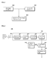
- FIG. 1 is a block diagram illustrating an example of a PLC system including an apparatus for detecting noise in a power supply of a PLC analog input/output module according to an exemplary embodiment of the present disclosure.
- the PLC system may include an analog module (100), a power supply (200) and a noise detection apparatus (300), and may further include other components. However, only components required for description of the present disclosure are illustrated herein.
- the analog module (100) may be an analog input module configured to convert an analog signal provided from a sub-device to a digital signal and provide the digital signal to an internal calculation process unit, and may be an analog output module configured to receive a digital signal reflecting a calculation process result provided by the calculation process unit, convert the digital signal to an analog signal, and provide the analog signal to the sub-device.
- the power supply (200) is a structure in order to supply a driving electric power required for driving the analog module (200).
- the power supply (200) convert electric power applied from the outside to an electric power of appropriate level for driving the analog module (100), and may provide the converted electric power to the analog module (100).
- the noise detection apparatus (300) may detect whether a noise is introduced in electric power outputted from the power supply (200).
- the structure of the noise detection apparatus (300) will be described hereinafter based on the enclosed drawings.
- FIG. 2 is a block diagram illustrating an apparatus for detecting noise in a power supply of a PLC analog input/output module according to an exemplary embodiment of the present disclosure
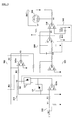
- FIG. 3 is a detailed circuit diagram of a PLC analog input/output module according to an exemplary embodiment of the present disclosure
- FIG. 4 is a view illustrating an example of output voltage waveform of each partial structure of an apparatus for detecting noise in a power supply of a PLC analog input/output module according to an exemplary embodiment of the present disclosure.
- the apparatus (300) for detecting noise in a power supply of a PLC analog input/output module may include a capacitor (310), a voltage conversion unit (320), a comparison unit (330), a reference voltage generation unit (340) and a determination unit (350).
- the capacitor (310) may be configured to extract a noise from a driving voltage outputted from the power supply (200).
- the capacitor (310) has a characteristic to block direct current ingredients, and the driving voltage is of direct current. Therefore, the output voltage of the capacitor (310) becomes '0', unless a noise is included in the driving current.
- the capacitor (310) outputs an alternate current voltage corresponding to the noise, when the noise is included in the driving voltage.
- the voltage (V 1 ) outputted from the capacitor (310) is used in order to determine whether a noised is included.
- the voltage (V 1 ) will be referred to as a 'noise determination target voltage'.
- the voltage conversion unit (320) may convert the noise determination target voltage in an alternate current form outputted from the capacitor (310) and output the converted noise determination target voltage.
- the voltage conversion unit (320) may output the noise determination target voltage, by half-wave rectifying and low pass filtering the noise determination target voltage. Detailed structure and operation of the voltage conversion unit (320) will be described hereinafter.
- the comparison unit (330) may compare the noise determination target voltage converted by the voltage conversion unit (320) with a reference voltage (Vref) outputted from the reference voltage generation unit (340) and may output the comparison result.
- the comparison result (V 6 ) may be a negative (-) or a positive (+) voltage.
- the volume of the negative (-) and the positive (+) voltage may be identical to each other.
- the comparison unit (330) may compare the noise determination target voltage with the reference voltage (Vref), and may output a negative (-) voltage when the noise determination target voltage is higher than the reference voltage, or output a positive (+) voltage when the noise determination target voltage is lower than the reference voltage.
- the comparison unit (330) may compare the noise determination target voltage with the reference voltage (Vref), and may output a positive (+) voltage when the noise determination target voltage is higher than the reference voltage, or output a negative (-) voltage when the noise determination target voltage is lower than the reference voltage.
- the reference voltage generation unit (340) may generate a reference voltage used for the comparison unit (330) to compare with the noise determination target voltage.
- the determination unit (350) may receive the comparison result outputted from the comparison unit (330), and may determine whether the noise determination target voltage is a noise and output the determination result.
- the determination unit (350) may be configured to output voltages of different levels based on the determination result.
- the determination unit (350) may be an NMOS (N-channel Metal-Oxide-Semiconductor) FET (Field Effect Transistor) or a PMOS (P-channel MOS) FET.
- the determination unit (350) may output a high level voltage when the comparison result received from the comparison unit (330) is a positive (+) voltage, or may output a low level voltage when the noise determination target voltage is a negative (-) voltage.
- the determination unit (350) may output a low level voltage when the comparison result received from the comparison unit (330) is a positive (+) voltage, or output a high level voltage when the noise determination target voltage is a negative (-) voltage.
- the voltage conversion unit (320) may include a half-wave rectifier (321), an inverting adder (322), an inverting amplifier (323) and a low pass filter (324).
- the half-wave rectifier (321) may half-wave rectify the noise determination target voltage having passed through the capacitor (310) ( FIG. 4(b) ).
- the inverting adder (322) may invert and add the noise determination target voltage that has been half-wave rectified by the half-wave rectifier (321) ( FIG. 4(c) ).
- the half-wave amplifier (323) may output the noise determination target voltage inverted and added by the inverting adder (322) as a voltage in an inverted waveform of the same volume ( FIG. 4(b) ), and the low pass filter (324) may low pass filter the noise determination target voltage inverted by the inverting amplifier (323) ( FIG. 4(e) ).
- the half-wave rectifier (321) may include first and second resistors (R1, R2), a first opi-amp (321 a), first and second diodes (D1, D2).
- a negative (-) input terminal the first opi-amp (321a) may be connected to the capacitor (310) and a positive (+) input terminal may be earthed.
- the first resistor (R1) may be connected between a negative (-) input terminal of the first opi-amp (321a) and the capacitor (310).
- An anode of the first diode (D1) may be connected between a negative (-) input terminal of the first opi-amp (321a) and the first resistor (R1), and a cathode of the first diode (D1) may be connected to an output terminal of the first opi-amp (321a).
- an anode of the second diode (D2) may be connected to an output terminal of the first opi-amp (321a), and a cathode of the second diode (D2) may be connected to an output side of the half-wave rectifier (321).
- a side of the second resistor (R2) may be connected between the first resistor (R1) and the first opi-amp (321a), and another side of the second resistor (R2) may be an output side of the half-wave rectifier (321).
- the second resistor (R2) may be connected to an anode of the first diode (D1) and a cathode of the second diode (D2).
- the first resistor (R1) and the second resistor (R2) are set as the same value, and when the noise determination target voltage (V1) is higher than zero (0), the first diode (D1) is turned on and the second diode (D2) is turned off so that the output voltage (V2) of the half-wave rectifier (321) becomes zero (0).
- the polarity of an area where the noise determination target voltage (V1) is under zero (0) may be changed and outputted as an output voltage (V2) of the half-wave rectifier (321).
- the inverting adder (322) may include third to fifth resistors (R3, R4, R5) and a second opi-amp (322a).
- a negative (-) input terminal of the second opi-amp (322a) may be connected to an output terminal of the half-wave rectifier (321), and a positive (+) input terminal of the second opi-amp (322a) may be earthed.
- the third resistor (R3) may be connected between negative (-) input terminals of the capacitor (310) and the second opi-amp (322a)
- the fourth resistor (R4) may be connected between an output terminal of the second opi-amp (322a) and a negative (-) input terminal of the second opi-amp (322a)
- the fifth resistor (R5) may be connected between an output side of the half-wave rectifier (321) and a negative (-) input terminal of the second opi-amp (322a).
- V 3 the output voltage (V 3 ) of the inverting adder (322) may be determined according to the following Equation 2.
- V 3 - R 4 R 3 V 1 + R 4 R 5
- V 2 - V 1 + 2 V 2
- the output voltage (V 3 ) of the inverting adder (322) may be outputted as a negative (-) waveform in the same volume as that of the noise determination target voltage (V 1 ).
- the inverting amplifier (323) may invert the output voltage (V 3 ) as a positive (+) waveform and output the inverted output voltage.
Landscapes
- Physics & Mathematics (AREA)
- General Physics & Mathematics (AREA)
- Engineering & Computer Science (AREA)
- Power Engineering (AREA)
- Programmable Controllers (AREA)
Abstract
Description
- The present disclosure relates to an apparatus for detecting noise in power supply of PLC analog input/output module. More particularly, the present disclosure relates to an apparatus for detecting noise in a power supply of a PLC analog input/output module which is capable of detecting whether a noise is introduced in electric power outputted by the power supply of the PLC analog input/output module.
- A PLC (Programmable Logic Controller) is a special computer capable of controlling various automated machines and processors. The PLC includes a memory storing programs and various data and may perform functions such as numerical calculation, logical calculation, sequencing control, timer, counter, etc.
- The PLC may be applied to various operations such as device control, device numerical setting, time control, real-time monitoring, real time data collection and safe device activation.
- The PLC includes an analog output module for providing signals to automation facility equipment, and an analog input module for receiving the signals output from the automation facility equipment. The analog input module plays a role of converting an analog signal delivered from the automation facility equipment into a digital signal and delivering the digital signal to an internal operation processing unit. In addition, the analog output module plays a role of receiving the digital signal from the operation processing unit, converting the digital signal into an analog signal and delivering the analog signal to the automation facility equipment.
- Here, a power supply configured to supply electric power for operation of the analog input/output module is provided. The power supply converts electric power inputted from the outside to the electric power required for operation of the analog input/output module, and supplies the electric power to the analog input/output module.
- Therefore, the electric power supplied by the power supply is required to be maintained stable, in order for the analog input/output module to be operated normally. In a case when a noise is introduced from the outside or a noise is generated in the PLC module, the output voltage of the power supply becomes unstable. When the unstable voltage is supplied to the analog input/output module, the analog input/output module can neither receive an accurate analog signal input nor output accurate analog signal. This phenomenon causes degradation in quality and performance of the product.
- Accordingly, the present disclosure is contrived to solve the foregoing disadvantages/problems of the related art, and an object of the present disclosure is to provide an apparatus for detecting noise in a power supply of a PLC analog input/output module which is capable of detecting whether a noise is introduced in electric power outputted by the power supply of the PLC analog input/output module.
- In a general aspect of the present disclosure, an apparatus for detecting noise in a power supply of a PLC analog input/output module is provided, the apparatus comprising: a capacitor configured to extract a noise determination target voltage from a driving voltage outputted from the power supply; a voltage conversion unit configured to convert the noise determination target voltage outputted from the capacitor and to output the converted noise determination target voltage; a comparison unit configured to compare the noise determination target voltage converted by the voltage conversion unit with a reference voltage; and a determination unit configured to determine whether the noise determination target voltage is a noise, based on a comparison result by the comparison unit.
- In some exemplary embodiments of the present disclosure, the voltage conversion unit may include: a half-wave rectifier configured to half-wave rectify the noise determination target voltage outputted from the capacitor; an inverting adder configured to invert and add the noise determination target voltage half-wave rectified by the half-wave rectifier; an inverting amplifier configured to output the noise detection determination target voltage inverted and added by the inverting adder in an inversed form of a same size; and a low pass filter configured to low-pass filter the noise determination target voltage inverted by the inverting amplifier.
- In some exemplary embodiments of the present disclosure, the comparison unit may output a positive voltage or a negative voltage when the noise determination target voltage is higher than the reference voltage, or may output a negative voltage or a positive voltage when the noise determination target voltage is lower than the reference voltage.
- In some exemplary embodiments of the present disclosure, the determination unit may output a high level voltage or a low level voltage when the noise determination target voltage is determined to be a noise, or may output a low level voltage or a high level voltage when the noise determination target voltage is determined not to be a noise.
- In some exemplary embodiments of the present disclosure, the determination unit may be an NMOS (N-channel Metal-Oxide-Semiconductor) FET (Field Effect Transistor) or a PMOS (P-channel MOS) FET configured to be turned on or turned off, according to the comparison result outputted from the comparison unit.
- According to an exemplary embodiment of the present disclosure, the apparatus for detecting noise in a power supply of a PLC analog input/output module may detect whether a noise is introduced in electric power outputted by the power supply of the PLC analog input/output module, when the power supply for supplying electric power to the PLC analog input/output module outputs an unstable voltage due to noise.
- Therefore, the noise introduced in electric power supplied by the power supply for supplying the electric power to the PLC analog input/output module is detected in advance, so that the noise may be prevented from being supplied to the PLC analog input/output module.
- As apparent from the foregoing, the malfunction occurrence rate of the PLC analog input/output module may be reduced, and thereby time and cost consumed in trouble shooting can also be reduced.
-
-
FIG. 1 is a block diagram illustrating an example of a PLC system including an apparatus for detecting noise in a power supply of a PLC analog input/output module according to an exemplary embodiment of the present disclosure. -
FIG. 2 is a block diagram illustrating an apparatus for detecting noise in a power supply of a PLC analog input/output module according to an exemplary embodiment of the present disclosure. -
FIG. 3 is a detailed circuit diagram of a PLC analog input/output module according to an exemplary embodiment of the present disclosure. -
FIG. 4 is a view illustrating an example of output voltage waveform of each partial structure of an apparatus for detecting noise in a power supply of a PLC analog input/output module according to an exemplary embodiment of the present disclosure. - Advantages and features of the present disclosure and methods to implement them will now be described more fully hereinafter with reference to exemplary embodiments accompanied by drawings. The present disclosure may, however, be embodied in different forms and should not be construed as limited to the embodiments set forth herein. Rather, these embodiments are provided so that this disclosure will be thorough and complete, and will fully convey the scope of the present disclosure to those skilled in the art. The scope of the present disclosure shall be defined only by the scope of claims. The same reference numbers indicate the same components throughout the specification. In the attached figures, the thickness of layers and regions may be exaggerated for clarity.
- When it is determined that a detailed description about known function or structure relating to the present disclosure may evade the main point of the present disclosure, the detailed description may be omitted. In addition, the meaning of specific terms or words used in the specification and claims should not be limited to the literal or commonly employed sense, but should be construed or may be different in accordance with the intention of a user or an operator and customary usages. Therefore, the definition of the specific terms or words should be based on the contents across the specification.
-
FIG. 1 is a block diagram illustrating an example of a PLC system including an apparatus for detecting noise in a power supply of a PLC analog input/output module according to an exemplary embodiment of the present disclosure. - Referring to
FIG. 1 , the PLC system may include an analog module (100), a power supply (200) and a noise detection apparatus (300), and may further include other components. However, only components required for description of the present disclosure are illustrated herein. - Here, the analog module (100) may be an analog input module configured to convert an analog signal provided from a sub-device to a digital signal and provide the digital signal to an internal calculation process unit, and may be an analog output module configured to receive a digital signal reflecting a calculation process result provided by the calculation process unit, convert the digital signal to an analog signal, and provide the analog signal to the sub-device.
- The power supply (200) is a structure in order to supply a driving electric power required for driving the analog module (200). The power supply (200) convert electric power applied from the outside to an electric power of appropriate level for driving the analog module (100), and may provide the converted electric power to the analog module (100).
- Meanwhile, the noise detection apparatus (300) may detect whether a noise is introduced in electric power outputted from the power supply (200). The structure of the noise detection apparatus (300) will be described hereinafter based on the enclosed drawings.
-
FIG. 2 is a block diagram illustrating an apparatus for detecting noise in a power supply of a PLC analog input/output module according to an exemplary embodiment of the present disclosure;FIG. 3 is a detailed circuit diagram of a PLC analog input/output module according to an exemplary embodiment of the present disclosure; andFIG. 4 is a view illustrating an example of output voltage waveform of each partial structure of an apparatus for detecting noise in a power supply of a PLC analog input/output module according to an exemplary embodiment of the present disclosure. - Referring to
FIGS. 2 to 4 , the apparatus (300) for detecting noise in a power supply of a PLC analog input/output module according to an exemplary embodiment of the present disclosure may include a capacitor (310), a voltage conversion unit (320), a comparison unit (330), a reference voltage generation unit (340) and a determination unit (350). - The capacitor (310) may be configured to extract a noise from a driving voltage outputted from the power supply (200).
- That is, the capacitor (310) has a characteristic to block direct current ingredients, and the driving voltage is of direct current. Therefore, the output voltage of the capacitor (310) becomes '0', unless a noise is included in the driving current.
- However, as illustrated in
FIG. 4 (a) , the capacitor (310) outputs an alternate current voltage corresponding to the noise, when the noise is included in the driving voltage. - The voltage (V1) outputted from the capacitor (310) is used in order to determine whether a noised is included. Thus, the voltage (V1) will be referred to as a 'noise determination target voltage'.
- The voltage conversion unit (320) may convert the noise determination target voltage in an alternate current form outputted from the capacitor (310) and output the converted noise determination target voltage.
- Here, the voltage conversion unit (320) may output the noise determination target voltage, by half-wave rectifying and low pass filtering the noise determination target voltage. Detailed structure and operation of the voltage conversion unit (320) will be described hereinafter.
- The comparison unit (330) may compare the noise determination target voltage converted by the voltage conversion unit (320) with a reference voltage (Vref) outputted from the reference voltage generation unit (340) and may output the comparison result.
- Here, as illustrated in
FIG. 4(f) , the comparison result (V6) may be a negative (-) or a positive (+) voltage. The volume of the negative (-) and the positive (+) voltage may be identical to each other. - Meanwhile, the comparison unit (330) may compare the noise determination target voltage with the reference voltage (Vref), and may output a negative (-) voltage when the noise determination target voltage is higher than the reference voltage, or output a positive (+) voltage when the noise determination target voltage is lower than the reference voltage.
- Selectively, the comparison unit (330) may compare the noise determination target voltage with the reference voltage (Vref), and may output a positive (+) voltage when the noise determination target voltage is higher than the reference voltage, or output a negative (-) voltage when the noise determination target voltage is lower than the reference voltage.
- The reference voltage generation unit (340) may generate a reference voltage used for the comparison unit (330) to compare with the noise determination target voltage.
- The determination unit (350) may receive the comparison result outputted from the comparison unit (330), and may determine whether the noise determination target voltage is a noise and output the determination result.
- Here, as illustrated in
FIG. 4(g) , the determination unit (350) may be configured to output voltages of different levels based on the determination result. The determination unit (350) may be an NMOS (N-channel Metal-Oxide-Semiconductor) FET (Field Effect Transistor) or a PMOS (P-channel MOS) FET. - As an example, the determination unit (350) may output a high level voltage when the comparison result received from the comparison unit (330) is a positive (+) voltage, or may output a low level voltage when the noise determination target voltage is a negative (-) voltage.
- Selectively, the determination unit (350) may output a low level voltage when the comparison result received from the comparison unit (330) is a positive (+) voltage, or output a high level voltage when the noise determination target voltage is a negative (-) voltage.
- Hereinafter, the structure and operation of the voltage conversion unit according to an exemplary embodiment of the present disclosure will be specifically described with reference to
FIGS. 3 and4 . - The voltage conversion unit (320) according to an exemplary embodiment of the present disclosure may include a half-wave rectifier (321), an inverting adder (322), an inverting amplifier (323) and a low pass filter (324).
- The half-wave rectifier (321) may half-wave rectify the noise determination target voltage having passed through the capacitor (310) (
FIG. 4(b) ). The inverting adder (322) may invert and add the noise determination target voltage that has been half-wave rectified by the half-wave rectifier (321) (FIG. 4(c) ). - The half-wave amplifier (323) may output the noise determination target voltage inverted and added by the inverting adder (322) as a voltage in an inverted waveform of the same volume (
FIG. 4(b) ), and the low pass filter (324) may low pass filter the noise determination target voltage inverted by the inverting amplifier (323) (FIG. 4(e) ). - Hereinafter, the structure requiring supplementary descriptions in the voltage conversion unit (320) will be further described. Descriptions for the generally used structure will be omitted.
- The half-wave rectifier (321) may include first and second resistors (R1, R2), a first opi-amp (321 a), first and second diodes (D1, D2).
- Here, a negative (-) input terminal the first opi-amp (321a) may be connected to the capacitor (310) and a positive (+) input terminal may be earthed. The first resistor (R1) may be connected between a negative (-) input terminal of the first opi-amp (321a) and the capacitor (310).
- An anode of the first diode (D1) may be connected between a negative (-) input terminal of the first opi-amp (321a) and the first resistor (R1), and a cathode of the first diode (D1) may be connected to an output terminal of the first opi-amp (321a).
- In addition, an anode of the second diode (D2) may be connected to an output terminal of the first opi-amp (321a), and a cathode of the second diode (D2) may be connected to an output side of the half-wave rectifier (321).
- Meanwhile, a side of the second resistor (R2) may be connected between the first resistor (R1) and the first opi-amp (321a), and another side of the second resistor (R2) may be an output side of the half-wave rectifier (321). Thus, the second resistor (R2) may be connected to an anode of the first diode (D1) and a cathode of the second diode (D2).
- When looking at operations of the half-wave rectifier (321) having such structure, in the case where the first resistor (R1) and the second resistor (R2) are set as the same value, and when the noise determination target voltage (V1) is higher than zero (0), the first diode (D1) is turned on and the second diode (D2) is turned off so that the output voltage (V2) of the half-wave rectifier (321) becomes zero (0).
- Contrariwise, when the noise determination target voltage (V1) is lower than zero (0), the first diode (D1) is turned off and the second diode (D2) is turned on, so that the output voltage (V2) of the half-wave rectifier (321) becomes -V1 according to the following Equation 1.

- Therefore, the polarity of an area where the noise determination target voltage (V1) is under zero (0) may be changed and outputted as an output voltage (V2) of the half-wave rectifier (321).
- Meanwhile, the inverting adder (322) may include third to fifth resistors (R3, R4, R5) and a second opi-amp (322a).
- A negative (-) input terminal of the second opi-amp (322a) may be connected to an output terminal of the half-wave rectifier (321), and a positive (+) input terminal of the second opi-amp (322a) may be earthed.
- The third resistor (R3) may be connected between negative (-) input terminals of the capacitor (310) and the second opi-amp (322a), the fourth resistor (R4) may be connected between an output terminal of the second opi-amp (322a) and a negative (-) input terminal of the second opi-amp (322a), and the fifth resistor (R5) may be connected between an output side of the half-wave rectifier (321) and a negative (-) input terminal of the second opi-amp (322a).
- When looking at operations of the inverting adder (322) having such structure, in the case where R3=R4 and R5=2R4, the output voltage (V3) of the inverting adder (322) may be determined according to the following Equation 2.

- Therefore, V2=0 when the noise determination target voltage (V1) is higher than zero (0), and therefore V3=-V1. In addition, V2=-V1 when the noise determination target voltage (V1) is lower than zero (0), and therefore V3=V1.
- To conclude, the output voltage (V3) of the inverting adder (322) may be outputted as a negative (-) waveform in the same volume as that of the noise determination target voltage (V1). The inverting amplifier (323) may invert the output voltage (V3) as a positive (+) waveform and output the inverted output voltage.
- Although an apparatus for detecting noise in a power supply of a PLC analog input/output module according to the present disclosure have been described with reference to a number of illustrative exemplary embodiments thereof, it should be understood that numerous other modifications and alternative embodiments can be devised by those skilled in the art that will fall within the spirit and scope of the principles of this invention. More particularly, various variations and modifications are possible in the component parts and/or arrangements of the subject combination arrangement within the scope of the disclosure, the drawing and the appended claims. In addition to variations and modifications in the component parts and/or arrangements, alternative uses will also be apparent to those skilled in the art.
- Therefore, the abovementioned exemplary embodiments and enclosed drawings are intended to be illustrative, and not to limit the scope of the claims. The scope of protection of the present disclosure is to be interpreted by the following claims, and that all the technical ideas within the equivalent scope of the scope of the present disclosure should be construed as being included.
Claims (5)
- An apparatus for detecting noise in a power supply of a PLC analog input/output module, the apparatus comprising:a capacitor configured to extract a noise determination target voltage from a driving voltage outputted from the power supply;a voltage conversion unit configured to convert the noise determination target voltage outputted from the capacitor and to output the converted noise determination target voltage;a comparison unit configured to compare the noise determination target voltage converted by the voltage conversion unit with a reference voltage; anda determination unit configured to determine whether the noise determination target voltage is a noise, based on a comparison result by the comparison unit.
- The apparatus of claim 1, wherein the voltage conversion unit includes:a half-wave rectifier configured to half-wave rectify the noise determination target voltage outputted from the capacitor;an inverting adder configured to invert and add the noise determination target voltage half-wave rectified by the half-wave rectifier;an inverting amplifier configured to output the noise detection determination target voltage inverted and added by the inverting adder in an inversed form of a same size; anda low pass filter configured to low-pass filter the noise determination target voltage inverted by the inverting amplifier.
- The apparatus of claim 1 or 2, wherein the comparison unit outputs a positive voltage or a negative voltage when the noise determination target voltage is higher than the reference voltage, or outputs a negative voltage or a positive voltage when the noise determination target voltage is lower than the reference voltage.
- The apparatus of any one of claims 1 to 3, wherein the determination unit outputs a high level voltage or a low level voltage when the noise determination target voltage is determined to be a noise, or outputs a low level voltage or a high level voltage when the noise determination target voltage is determined not to be a noise.
- The apparatus of any one of claims 1 to 4, wherein the determination unit is an NMOS (N-channel Metal-Oxide-Semiconductor) FET (Field Effect Transistor) or a PMOS (P-channel MOS) FET configured to be turned on or turned off, according to the comparison result outputted from the comparison unit.
Applications Claiming Priority (1)
| Application Number | Priority Date | Filing Date | Title |
|---|---|---|---|
| KR1020150008573A KR101984548B1 (en) | 2015-01-19 | 2015-01-19 | Apparatus for detecting noise in Power Supply of PLC Analogue Input and Output Module |
Publications (1)
| Publication Number | Publication Date |
|---|---|
| EP3051300A1 true EP3051300A1 (en) | 2016-08-03 |
Family
ID=55085589
Family Applications (1)
| Application Number | Title | Priority Date | Filing Date |
|---|---|---|---|
| EP16150737.1A Withdrawn EP3051300A1 (en) | 2015-01-19 | 2016-01-11 | Apparatus for detecting noise in power supply of plc analogue input and output module |
Country Status (5)
| Country | Link |
|---|---|
| US (1) | US9778292B2 (en) |
| EP (1) | EP3051300A1 (en) |
| JP (1) | JP6093050B2 (en) |
| KR (1) | KR101984548B1 (en) |
| CN (1) | CN105807149B (en) |
Families Citing this family (5)
| Publication number | Priority date | Publication date | Assignee | Title |
|---|---|---|---|---|
| CN111239476B (en) * | 2018-11-29 | 2022-11-22 | 瑞昱半导体股份有限公司 | Signal detector and signal detection method |
| JP6970140B2 (en) * | 2019-05-23 | 2021-11-24 | 株式会社ソニー・インタラクティブエンタテインメント | Power supply unit inspection device |
| CN113452237B (en) * | 2020-03-26 | 2022-06-24 | 立锜科技股份有限公司 | Power supply controller with reduced audio noise and method for reducing audio noise |
| WO2023053246A1 (en) * | 2021-09-29 | 2023-04-06 | 三菱電機株式会社 | Noise detection device and plc system |
| CN117969978A (en) * | 2022-10-25 | 2024-05-03 | 华为技术有限公司 | Power supply noise detection circuit and working method, jitter limiting circuit, and electronic equipment |
Citations (3)
| Publication number | Priority date | Publication date | Assignee | Title |
|---|---|---|---|---|
| US4692692A (en) * | 1984-10-05 | 1987-09-08 | Commissariat A L'energie Atomique | Electronic apparatus for detecting stray variations in an electrical voltage as a function of time |
| US4694193A (en) * | 1983-05-27 | 1987-09-15 | Siemens Aktiengesellschaft | Fault recognition circuit for parallel power supply devices feeding a user |
| US5119073A (en) * | 1990-09-05 | 1992-06-02 | Nelson Glenn M | AC ripple meter |
Family Cites Families (17)
| Publication number | Priority date | Publication date | Assignee | Title |
|---|---|---|---|---|
| US4520310A (en) * | 1982-06-18 | 1985-05-28 | Sycon Corporation | Autofunction voltmeter |
| JPH0382402A (en) | 1989-08-28 | 1991-04-08 | Matsushita Electric Works Ltd | Dryer |
| JPH0382402U (en) * | 1989-12-11 | 1991-08-22 | ||
| US5289166A (en) * | 1991-10-04 | 1994-02-22 | Lambda Electronics Inc. | Voltage detector |
| JP3179838B2 (en) | 1992-02-18 | 2001-06-25 | 株式会社東芝 | Noise detection circuit |
| US5479095A (en) * | 1994-06-30 | 1995-12-26 | Power Corporation Of America | Method and apparatus for measurement of AC and DC electrical current |
| JPH10303991A (en) | 1997-04-23 | 1998-11-13 | Matsushita Electric Works Ltd | Display unit |
| JP3857652B2 (en) * | 2001-04-18 | 2006-12-13 | 富士通株式会社 | Distortion compensation device |
| US7007305B2 (en) * | 2001-09-06 | 2006-02-28 | Genlyte Thomas Group Llc | Repeater amplifier with signal firewall protection for power line carrier communication networks |
| KR200300696Y1 (en) * | 2002-09-24 | 2003-01-14 | 주식회사 어텍 | Apparatus for respectively controlling street lamps by PLC |
| US7949372B2 (en) * | 2006-02-27 | 2011-05-24 | Power Science Inc. | Data communications enabled by wire free power transfer |
| JP4893931B2 (en) | 2006-05-19 | 2012-03-07 | オムロン株式会社 | Safety controller |
| JP2010039739A (en) | 2008-08-05 | 2010-02-18 | Koyo Electronics Ind Co Ltd | Safe plc (programmable logic controller) |
| CN201607480U (en) * | 2009-11-13 | 2010-10-13 | 英业达股份有限公司 | Power Signal Test Set |
| CN201765265U (en) * | 2010-07-23 | 2011-03-16 | 上海松下电工自动化控制有限公司 | Detector for power panel |
| CN102467221A (en) * | 2010-11-18 | 2012-05-23 | 英业达股份有限公司 | Apparatus and method for detecting noise interference in a power supply signal |
| US9407323B2 (en) * | 2013-01-18 | 2016-08-02 | Marvell World Trade Ltd. | Devices and methods for power consumption control in powerline communications systems and apparatus |
-
2015
- 2015-01-19 KR KR1020150008573A patent/KR101984548B1/en not_active Expired - Fee Related
- 2015-12-29 US US14/983,305 patent/US9778292B2/en not_active Expired - Fee Related
-
2016
- 2016-01-11 CN CN201610016527.2A patent/CN105807149B/en not_active Expired - Fee Related
- 2016-01-11 EP EP16150737.1A patent/EP3051300A1/en not_active Withdrawn
- 2016-01-18 JP JP2016006910A patent/JP6093050B2/en not_active Expired - Fee Related
Patent Citations (3)
| Publication number | Priority date | Publication date | Assignee | Title |
|---|---|---|---|---|
| US4694193A (en) * | 1983-05-27 | 1987-09-15 | Siemens Aktiengesellschaft | Fault recognition circuit for parallel power supply devices feeding a user |
| US4692692A (en) * | 1984-10-05 | 1987-09-08 | Commissariat A L'energie Atomique | Electronic apparatus for detecting stray variations in an electrical voltage as a function of time |
| US5119073A (en) * | 1990-09-05 | 1992-06-02 | Nelson Glenn M | AC ripple meter |
Non-Patent Citations (3)
| Title |
|---|
| DUCU DRAGOS: "An1353 - Op Amp Rectifiers, Peak Detectors and Clamps", 1 March 2011 (2011-03-01), XP055279782, Retrieved from the Internet <URL:http://ww1.microchip.com/downloads/en/AppNotes/01353A.pdf> [retrieved on 20160610] * |
| HANK ZUMBHALEN: "Full Wave Rectifier", 1 March 2013 (2013-03-01), XP055279783, Retrieved from the Internet <URL:http://www.analog.com/media/en/training-seminars/tutorials/MT-211.pdf> [retrieved on 20160610] * |
| JAMES BRYANT: "Using Op Amps as Comparators", 1 November 2011 (2011-11-01), XP055280481, Retrieved from the Internet <URL:http://www.analog.com/media/en/technical-documentation/application-notes/AN-849.pdf> [retrieved on 20160614] * |
Also Published As
| Publication number | Publication date |
|---|---|
| CN105807149A (en) | 2016-07-27 |
| KR20160089099A (en) | 2016-07-27 |
| US9778292B2 (en) | 2017-10-03 |
| JP6093050B2 (en) | 2017-03-08 |
| US20160216297A1 (en) | 2016-07-28 |
| KR101984548B1 (en) | 2019-05-31 |
| JP2016134181A (en) | 2016-07-25 |
| CN105807149B (en) | 2018-11-27 |
Similar Documents
| Publication | Publication Date | Title |
|---|---|---|
| US9778292B2 (en) | Apparatus for detecting noise in power supply of PLC analogue input and output module | |
| US7352155B2 (en) | Apparatus and method for detecting battery pack voltage | |
| US20130326241A1 (en) | Power supply circuit to simulate battery power | |
| CN108195465B (en) | Optical signal detection device and method | |
| US20130026974A1 (en) | Charging circuit and charging control method | |
| KR101735869B1 (en) | Apparatus for Detecting Surge Voltage using Shunt Regulator | |
| US10291044B2 (en) | Battery charger and control method thereof | |
| US9601987B2 (en) | Power supply apparatus | |
| EP2950110B1 (en) | Broad-range current measurement using duty cycling | |
| EP3447880A1 (en) | Ac-ok detection circuit and method | |
| US8976498B2 (en) | Field device for determining and/or monitoring a physical or chemical process variable | |
| EP3015830A1 (en) | Standard signal generator | |
| US11025158B2 (en) | Power supply apparatus capable to extend hold-up time length of output voltage | |
| EP2728766B1 (en) | Disconnection detecting apparatus and method | |
| CN105391320B (en) | Polyphase source circuit | |
| US9417644B2 (en) | Apparatus for and method of controlling power supply system | |
| US9594416B2 (en) | Analog current output module | |
| US9831761B2 (en) | Speedy discharging circuit and power supply apparatus with speedy discharging circuit | |
| US8141425B2 (en) | Angular rate detection apparatus providing stable output | |
| US20140189412A1 (en) | Time sequence circuit for power supply unit | |
| US20130207597A1 (en) | Charge circuit | |
| US20130300398A1 (en) | Discharge test circuit for testing whether there is current on a circuit board | |
| US10279472B2 (en) | Servo control system and robot | |
| CN111351504A (en) | Current frequency conversion device and system with programmable scale factors | |
| US8321694B2 (en) | Power supply circuit for south bridge chip |
Legal Events
| Date | Code | Title | Description |
|---|---|---|---|
| PUAI | Public reference made under article 153(3) epc to a published international application that has entered the european phase |
Free format text: ORIGINAL CODE: 0009012 |
|
| AK | Designated contracting states |
Kind code of ref document: A1 Designated state(s): AL AT BE BG CH CY CZ DE DK EE ES FI FR GB GR HR HU IE IS IT LI LT LU LV MC MK MT NL NO PL PT RO RS SE SI SK SM TR |
|
| AX | Request for extension of the european patent |
Extension state: BA ME |
|
| STAA | Information on the status of an ep patent application or granted ep patent |
Free format text: STATUS: REQUEST FOR EXAMINATION WAS MADE |
|
| 17P | Request for examination filed |
Effective date: 20170203 |
|
| RBV | Designated contracting states (corrected) |
Designated state(s): AL AT BE BG CH CY CZ DE DK EE ES FI FR GB GR HR HU IE IS IT LI LT LU LV MC MK MT NL NO PL PT RO RS SE SI SK SM TR |
|
| STAA | Information on the status of an ep patent application or granted ep patent |
Free format text: STATUS: EXAMINATION IS IN PROGRESS |
|
| 17Q | First examination report despatched |
Effective date: 20180323 |
|
| STAA | Information on the status of an ep patent application or granted ep patent |
Free format text: STATUS: THE APPLICATION IS DEEMED TO BE WITHDRAWN |
|
| 18D | Application deemed to be withdrawn |
Effective date: 20220802 |