EP3048728A1 - Electronic equipment and automobile mounting the same - Google Patents
Electronic equipment and automobile mounting the same Download PDFInfo
- Publication number
- EP3048728A1 EP3048728A1 EP16152176.0A EP16152176A EP3048728A1 EP 3048728 A1 EP3048728 A1 EP 3048728A1 EP 16152176 A EP16152176 A EP 16152176A EP 3048728 A1 EP3048728 A1 EP 3048728A1
- Authority
- EP
- European Patent Office
- Prior art keywords
- joint layer
- electromigration
- progression index
- low potential
- high potential
- Prior art date
- Legal status (The legal status is an assumption and is not a legal conclusion. Google has not performed a legal analysis and makes no representation as to the accuracy of the status listed.)
- Granted
Links
Images




Classifications
-
- H—ELECTRICITY
- H03—ELECTRONIC CIRCUITRY
- H03K—PULSE TECHNIQUE
- H03K17/00—Electronic switching or gating, i.e. not by contact-making and –breaking
- H03K17/16—Modifications for eliminating interference voltages or currents
- H03K17/168—Modifications for eliminating interference voltages or currents in composite switches
-
- B—PERFORMING OPERATIONS; TRANSPORTING
- B60—VEHICLES IN GENERAL
- B60L—PROPULSION OF ELECTRICALLY-PROPELLED VEHICLES; SUPPLYING ELECTRIC POWER FOR AUXILIARY EQUIPMENT OF ELECTRICALLY-PROPELLED VEHICLES; ELECTRODYNAMIC BRAKE SYSTEMS FOR VEHICLES IN GENERAL; MAGNETIC SUSPENSION OR LEVITATION FOR VEHICLES; MONITORING OPERATING VARIABLES OF ELECTRICALLY-PROPELLED VEHICLES; ELECTRIC SAFETY DEVICES FOR ELECTRICALLY-PROPELLED VEHICLES
- B60L3/00—Electric devices on electrically-propelled vehicles for safety purposes; Monitoring operating variables, e.g. speed, deceleration or energy consumption
- B60L3/0023—Detecting, eliminating, remedying or compensating for drive train abnormalities, e.g. failures within the drive train
- B60L3/003—Detecting, eliminating, remedying or compensating for drive train abnormalities, e.g. failures within the drive train relating to inverters
-
- H—ELECTRICITY
- H10—SEMICONDUCTOR DEVICES; ELECTRIC SOLID-STATE DEVICES NOT OTHERWISE PROVIDED FOR
- H10W—GENERIC PACKAGES, INTERCONNECTIONS, CONNECTORS OR OTHER CONSTRUCTIONAL DETAILS OF DEVICES COVERED BY CLASS H10
- H10W72/00—Interconnections or connectors in packages
- H10W72/30—Die-attach connectors
-
- B—PERFORMING OPERATIONS; TRANSPORTING
- B60—VEHICLES IN GENERAL
- B60L—PROPULSION OF ELECTRICALLY-PROPELLED VEHICLES; SUPPLYING ELECTRIC POWER FOR AUXILIARY EQUIPMENT OF ELECTRICALLY-PROPELLED VEHICLES; ELECTRODYNAMIC BRAKE SYSTEMS FOR VEHICLES IN GENERAL; MAGNETIC SUSPENSION OR LEVITATION FOR VEHICLES; MONITORING OPERATING VARIABLES OF ELECTRICALLY-PROPELLED VEHICLES; ELECTRIC SAFETY DEVICES FOR ELECTRICALLY-PROPELLED VEHICLES
- B60L3/00—Electric devices on electrically-propelled vehicles for safety purposes; Monitoring operating variables, e.g. speed, deceleration or energy consumption
- B60L3/0023—Detecting, eliminating, remedying or compensating for drive train abnormalities, e.g. failures within the drive train
- B60L3/0084—Detecting, eliminating, remedying or compensating for drive train abnormalities, e.g. failures within the drive train relating to control modules
-
- B—PERFORMING OPERATIONS; TRANSPORTING
- B60—VEHICLES IN GENERAL
- B60L—PROPULSION OF ELECTRICALLY-PROPELLED VEHICLES; SUPPLYING ELECTRIC POWER FOR AUXILIARY EQUIPMENT OF ELECTRICALLY-PROPELLED VEHICLES; ELECTRODYNAMIC BRAKE SYSTEMS FOR VEHICLES IN GENERAL; MAGNETIC SUSPENSION OR LEVITATION FOR VEHICLES; MONITORING OPERATING VARIABLES OF ELECTRICALLY-PROPELLED VEHICLES; ELECTRIC SAFETY DEVICES FOR ELECTRICALLY-PROPELLED VEHICLES
- B60L50/00—Electric propulsion with power supplied within the vehicle
- B60L50/50—Electric propulsion with power supplied within the vehicle using propulsion power supplied by batteries or fuel cells
- B60L50/51—Electric propulsion with power supplied within the vehicle using propulsion power supplied by batteries or fuel cells characterised by AC-motors
-
- B—PERFORMING OPERATIONS; TRANSPORTING
- B60—VEHICLES IN GENERAL
- B60L—PROPULSION OF ELECTRICALLY-PROPELLED VEHICLES; SUPPLYING ELECTRIC POWER FOR AUXILIARY EQUIPMENT OF ELECTRICALLY-PROPELLED VEHICLES; ELECTRODYNAMIC BRAKE SYSTEMS FOR VEHICLES IN GENERAL; MAGNETIC SUSPENSION OR LEVITATION FOR VEHICLES; MONITORING OPERATING VARIABLES OF ELECTRICALLY-PROPELLED VEHICLES; ELECTRIC SAFETY DEVICES FOR ELECTRICALLY-PROPELLED VEHICLES
- B60L50/00—Electric propulsion with power supplied within the vehicle
- B60L50/50—Electric propulsion with power supplied within the vehicle using propulsion power supplied by batteries or fuel cells
- B60L50/60—Electric propulsion with power supplied within the vehicle using propulsion power supplied by batteries or fuel cells using power supplied by batteries
-
- H—ELECTRICITY
- H03—ELECTRONIC CIRCUITRY
- H03K—PULSE TECHNIQUE
- H03K17/00—Electronic switching or gating, i.e. not by contact-making and –breaking
- H03K17/51—Electronic switching or gating, i.e. not by contact-making and –breaking characterised by the components used
- H03K17/56—Electronic switching or gating, i.e. not by contact-making and –breaking characterised by the components used by the use, as active elements, of semiconductor devices
- H03K17/567—Circuits characterised by the use of more than one type of semiconductor device, e.g. BIMOS, composite devices such as IGBT
-
- H—ELECTRICITY
- H03—ELECTRONIC CIRCUITRY
- H03K—PULSE TECHNIQUE
- H03K17/00—Electronic switching or gating, i.e. not by contact-making and –breaking
- H03K17/51—Electronic switching or gating, i.e. not by contact-making and –breaking characterised by the components used
- H03K17/56—Electronic switching or gating, i.e. not by contact-making and –breaking characterised by the components used by the use, as active elements, of semiconductor devices
- H03K17/687—Electronic switching or gating, i.e. not by contact-making and –breaking characterised by the components used by the use, as active elements, of semiconductor devices the devices being field-effect transistors
- H03K17/6871—Electronic switching or gating, i.e. not by contact-making and –breaking characterised by the components used by the use, as active elements, of semiconductor devices the devices being field-effect transistors the output circuit comprising more than one controlled field-effect transistor
-
- B—PERFORMING OPERATIONS; TRANSPORTING
- B60—VEHICLES IN GENERAL
- B60L—PROPULSION OF ELECTRICALLY-PROPELLED VEHICLES; SUPPLYING ELECTRIC POWER FOR AUXILIARY EQUIPMENT OF ELECTRICALLY-PROPELLED VEHICLES; ELECTRODYNAMIC BRAKE SYSTEMS FOR VEHICLES IN GENERAL; MAGNETIC SUSPENSION OR LEVITATION FOR VEHICLES; MONITORING OPERATING VARIABLES OF ELECTRICALLY-PROPELLED VEHICLES; ELECTRIC SAFETY DEVICES FOR ELECTRICALLY-PROPELLED VEHICLES
- B60L2210/00—Converter types
- B60L2210/10—DC to DC converters
-
- H—ELECTRICITY
- H02—GENERATION; CONVERSION OR DISTRIBUTION OF ELECTRIC POWER
- H02M—APPARATUS FOR CONVERSION BETWEEN AC AND AC, BETWEEN AC AND DC, OR BETWEEN DC AND DC, AND FOR USE WITH MAINS OR SIMILAR POWER SUPPLY SYSTEMS; CONVERSION OF DC OR AC INPUT POWER INTO SURGE OUTPUT POWER; CONTROL OR REGULATION THEREOF
- H02M1/00—Details of apparatus for conversion
- H02M1/32—Means for protecting converters other than automatic disconnection
-
- H—ELECTRICITY
- H02—GENERATION; CONVERSION OR DISTRIBUTION OF ELECTRIC POWER
- H02M—APPARATUS FOR CONVERSION BETWEEN AC AND AC, BETWEEN AC AND DC, OR BETWEEN DC AND DC, AND FOR USE WITH MAINS OR SIMILAR POWER SUPPLY SYSTEMS; CONVERSION OF DC OR AC INPUT POWER INTO SURGE OUTPUT POWER; CONTROL OR REGULATION THEREOF
- H02M3/00—Conversion of DC power input into DC power output
- H02M3/02—Conversion of DC power input into DC power output without intermediate conversion into AC
- H02M3/04—Conversion of DC power input into DC power output without intermediate conversion into AC by static converters
- H02M3/10—Conversion of DC power input into DC power output without intermediate conversion into AC by static converters using discharge tubes with control electrode or semiconductor devices with control electrode
- H02M3/145—Conversion of DC power input into DC power output without intermediate conversion into AC by static converters using discharge tubes with control electrode or semiconductor devices with control electrode using devices of a triode or transistor type requiring continuous application of a control signal
- H02M3/155—Conversion of DC power input into DC power output without intermediate conversion into AC by static converters using discharge tubes with control electrode or semiconductor devices with control electrode using devices of a triode or transistor type requiring continuous application of a control signal using semiconductor devices only
- H02M3/156—Conversion of DC power input into DC power output without intermediate conversion into AC by static converters using discharge tubes with control electrode or semiconductor devices with control electrode using devices of a triode or transistor type requiring continuous application of a control signal using semiconductor devices only with automatic control of output voltage or current, e.g. switching regulators
- H02M3/158—Conversion of DC power input into DC power output without intermediate conversion into AC by static converters using discharge tubes with control electrode or semiconductor devices with control electrode using devices of a triode or transistor type requiring continuous application of a control signal using semiconductor devices only with automatic control of output voltage or current, e.g. switching regulators including plural semiconductor devices as final control devices for a single load
-
- H—ELECTRICITY
- H03—ELECTRONIC CIRCUITRY
- H03K—PULSE TECHNIQUE
- H03K19/00—Logic circuits, i.e. having at least two inputs acting on one output; Inverting circuits
- H03K19/003—Modifications for increasing the reliability for protection
-
- H—ELECTRICITY
- H10—SEMICONDUCTOR DEVICES; ELECTRIC SOLID-STATE DEVICES NOT OTHERWISE PROVIDED FOR
- H10W—GENERIC PACKAGES, INTERCONNECTIONS, CONNECTORS OR OTHER CONSTRUCTIONAL DETAILS OF DEVICES COVERED BY CLASS H10
- H10W72/00—Interconnections or connectors in packages
- H10W72/071—Connecting or disconnecting
- H10W72/073—Connecting or disconnecting of die-attach connectors
- H10W72/07351—Connecting or disconnecting of die-attach connectors characterised by changes in properties of the die-attach connectors during connecting
- H10W72/07354—Connecting or disconnecting of die-attach connectors characterised by changes in properties of the die-attach connectors during connecting changes in dispositions
-
- H—ELECTRICITY
- H10—SEMICONDUCTOR DEVICES; ELECTRIC SOLID-STATE DEVICES NOT OTHERWISE PROVIDED FOR
- H10W—GENERIC PACKAGES, INTERCONNECTIONS, CONNECTORS OR OTHER CONSTRUCTIONAL DETAILS OF DEVICES COVERED BY CLASS H10
- H10W72/00—Interconnections or connectors in packages
- H10W72/30—Die-attach connectors
- H10W72/341—Dispositions of die-attach connectors, e.g. layouts
-
- Y—GENERAL TAGGING OF NEW TECHNOLOGICAL DEVELOPMENTS; GENERAL TAGGING OF CROSS-SECTIONAL TECHNOLOGIES SPANNING OVER SEVERAL SECTIONS OF THE IPC; TECHNICAL SUBJECTS COVERED BY FORMER USPC CROSS-REFERENCE ART COLLECTIONS [XRACs] AND DIGESTS
- Y02—TECHNOLOGIES OR APPLICATIONS FOR MITIGATION OR ADAPTATION AGAINST CLIMATE CHANGE
- Y02T—CLIMATE CHANGE MITIGATION TECHNOLOGIES RELATED TO TRANSPORTATION
- Y02T10/00—Road transport of goods or passengers
- Y02T10/60—Other road transportation technologies with climate change mitigation effect
- Y02T10/70—Energy storage systems for electromobility, e.g. batteries
-
- Y—GENERAL TAGGING OF NEW TECHNOLOGICAL DEVELOPMENTS; GENERAL TAGGING OF CROSS-SECTIONAL TECHNOLOGIES SPANNING OVER SEVERAL SECTIONS OF THE IPC; TECHNICAL SUBJECTS COVERED BY FORMER USPC CROSS-REFERENCE ART COLLECTIONS [XRACs] AND DIGESTS
- Y02—TECHNOLOGIES OR APPLICATIONS FOR MITIGATION OR ADAPTATION AGAINST CLIMATE CHANGE
- Y02T—CLIMATE CHANGE MITIGATION TECHNOLOGIES RELATED TO TRANSPORTATION
- Y02T10/00—Road transport of goods or passengers
- Y02T10/60—Other road transportation technologies with climate change mitigation effect
- Y02T10/72—Electric energy management in electromobility
Definitions
- the present specification discloses an electronic equipment in which a semiconductor device having an electrode exposed on a surface of the semiconductor device is joined to an electric conductor via a joint layer, and also discloses an automobile on which the electronic equipment is mounted.
- a semiconductor device including an electrode exposed on a surface of the semiconductor device is used under a state where the electrode is joined to an electric conductor via a joint layer.
- Current flows through the joint layer.
- a phenomenon occurs in which ions in the joint layer are moved.
- this phenomenon is called electromigration, and may be abbreviated as EM.
- Progression of EM leads to occurrence of a defect in the joint layer, and thus results in unstable operation of the semiconductor device or an electronic equipment including the semiconductor device.
- Japanese Patent Application Publication No. 2013-175578 discloses a technology for suppressing the progression of EM.
- a metal layer that suppresses the progression of EM is added.
- an object of the present specification is to provide a technology that suppresses the progression of EM without the addition of a metal layer.
- a semiconductor device passes current bidirectionally, and a direction of current is switched over time between a state in which forward current flows through a joint layer and a state in which reverse current flows through the joint layer.
- the technology described in the present specification is useful for an electric automobile which includes a motor and a drive wheel and travels by rotating the drive wheel with the motor.
- the "electric automobile” described here includes an electric automobile in which power is supplied from a battery to a motor, a fuel battery automobile in which power is supplied from a fuel battery to a motor, an automobile in which power is supplied from a generator driven by an engine to a motor, and a hybrid automobile which includes an engine in addition to a motor and in which a drive wheel is rotated by the motor and/or the engine.
- the electric automobile in which the drive wheel is driven by the motor includes an electric power conversion equipment that is connected to the motor.
- an automobile which includes a bidirectional converter, having both a voltage boosting function and a voltage reducing function, boosts a battery voltage, supplies the boosted voltage to a motor, reduces a voltage generated by the motor operating as a generator and charges the battery by the reduced voltage.
- the bidirectional converter is part of the electric power conversion equipment.
- power running or "power running operation”
- regeneration or "regeneration operation”.
- the electric power conversion equipment at the time of power running boosts a battery voltage to convert it into a motor drive current
- the electric power conversion equipment at the time of regeneration converts power generated by the motor into a charge current of the battery.
- the motor in this context may be referred to as a "motor generator” by focusing attention on the fact that the motor serves as a motor or a generator, in the present specification the motor is simply referred to as a motor.
- a motor or both the motor and the drive wheel can be rotated by an engine. This is also the regeneration.
- a semiconductor device passes current bidirectionally, and a direction of current is switched over time between a state in which forward current flows through a joint layer and a state in which reverse current flows through the joint layer.
- an IGBT 12 and a diode 14 are connected in parallel, and a high potential electrode 16 and a low potential electrode 18 are exposed on a surface of the semiconductor device 10, respectively.
- the high potential electrode 16 is connected via a high potential joint layer 20 to an unillustrated high potential electric conductor
- the low potential electrode 18 is connected via a low potential joint layer 22 to an unillustrated low potential electric conductor.
- the semiconductor device 10 is bidirectional, and in the semiconductor device 10, as shown by arrows (a), current may flow from the high potential electrode 16 toward the low potential electrode 18 via the IGBT 12, or as shown by arrows (b), current may flow from the low potential electrode 18 toward the high potential electrode 16 via the diode 14.
- a potential of the low potential electrode 18 may be temporarily higher than that of the high potential electrode 16, and thus reverse current may flow.
- the current flowing from the high potential electrode 16 toward the low potential electrode 18 is referred to as forward current
- the current flowing from the low potential electrode 18 toward the high potential electrode 16 in a transient state or the like is referred to as reverse current.
- the semiconductor device 10 of FIG. 1(1) passes current bidirectionally, and the direction of the current is switched over time between a state in which the forward current flows and a state in which the reverse current flows. Accordingly, the direction of the current is switched over time between a state where the forward current flows through the joint layers 20 and 22 and a state where the reverse current flows through the joint layers 20 and 22.
- the electronic equipment disclosed in the present specification comprises a calculator and a controller.
- the calculator is configured to calculate an imbalance EM progression index.
- the imbalance EM progression index is a difference between a progression index (in the present specification, referred to as a forward current EM progression index) of EM generated in the joint layer due to the flowing of the forward current through the joint layer and a progression index (referred to as a reverse current EM progression index) of EM generated in the joint layer due to the flowing of the reverse current through the joint layer.
- the controller is configured to cause phenomena that suppress the progression of the EM by cancelling out the forward current EM with the reverse current EM and alternatively by cancelling out the reverse current EM with the forward current EM.
- the controller is configured to (adopt a condition to) speed up an increase rate of the reverse current EM progression index in at least a part of an excessive forward current EM period during which the forward current EM progression index is larger than the reverse current EM progression index. Also, the controller is configured to (adopt a condition to) speed up an increase rate of the forward current EM progression index in at least a part of an excessive reverse current EM period during which the reverse current EM progression index is larger than the forward current EM progression index.
- the controller is configured to (adopt the condition to) speed up the increase rate of the reverse current EM progression index.
- the controller is configured to (adopt the condition to) speed up the increase rate of the progression index of the EM caused by the reverse current.
- the controller is configured to (adopt the condition to) speed up the increase rate of the forward current EM progression index. Hence, the excessive EM generated by the reverse current is cancelled out by the subsequent forward current, and thereby the imbalance amount of EM is reduced.
- FIG. 1(1) shows a semiconductor device 10 ⁇ that incorporates a MOS, and even in the semiconductor device 10 ⁇ , a direction of current is switched over time between a state in which forward current flows through joint layers 20 ⁇ and 22 ⁇ and a state in which a reverse current flows through joint layers 20 ⁇ and 22 ⁇ .
- the technology described in the present specification is also useful for the semiconductor device shown in FIG. 1(2) .
- the direction of the current is switched over time among a direction shown by an arrow (a2) indicating a state where the forward current flows through the joint layer 22 ⁇ , a direction shown by an arrow (b1) indicating a state where the reverse current flows through the joint layer 20 ⁇ , a direction shown by an arrow (a1) indicating a state where the forward current flows through the joint layer 20 ⁇ and a direction shown by an arrow (b2) indicating a state where the reverse current flows through the joint layer 22 ⁇ .
- the state where the forward current flows through the joint layer 20 ⁇ and the state where the forward current flows through the joint layer 22 ⁇ occur at different times, and the state where the reverse current flows through the joint layer 20 ⁇ and the state where the reverse current flows through the joint layer 22 ⁇ occur at different times.
- a magnitude of the current flowing through the joint layer 20 ⁇ differs from a magnitude of the current flowing through the joint layer 22 ⁇ .
- the technology described in the present specification can be applied to the semiconductor device shown in FIG. 1(3) , that is, the equipment having two or more joint layers 20 ⁇ and 22 ⁇ that differ in the direction of the current being passed and a value of the current being passed.
- the technology can also be applied to an electronic equipment that has three or more joint layers 20 ⁇ , 22 ⁇ and 38 ⁇ .
- the semiconductor device 10 ⁇ of FIG. 1(3), FIG. 1(2) can equally incorporate a MOS in each of the parallel circuits as well.
- the semiconductor devices shown in FIGS. 1(1) and 1(2) may form an upper arm or a lower arm in a bidirectional converter (having both a voltage boosting function and a voltage reducing function) mounted on an electric automobile.
- the semiconductor device shown in FIG. 1(3) may form a bidirectional converter mounted on an electric automobile.
- the technology described in the present specification can be applied to any joint layer via which a semiconductor device configuring a bidirectional converter mounted on an electric automobile is joined to an electric conductor.
- the controller may increase a temperature of the joint layer when the reverse current flows in the at least part of the excessive forward current EM period, and may increase the temperature of the joint layer when the forward current flows in the at least part of the excessive reverse current EM period.
- the progression rate of the EM is increased.
- the increase rate of the progression index of the EM is speeded up.
- the increase rate of the progression index of the EM caused by the reverse current is speeded up. Therefore, the imbalance amount in which the forward current EM is excessive is reduced while the reverse current is being passed. As a result, the EM actually being generated in the joint layer is reduced.
- the increase rate of the progression index of the EM caused by the forward current is speeded up. Therefore, the imbalance amount in which the reverse current EM is excessive is reduced while the forward current is being passed. As a result, the EM actually being generated in the joint layer is reduced.
- the controller may increase occasions at which the reverse current flows during the excessive forward current EM period, and may increase occasions at which the forward current flows during the excessive reverse current EM period.
- adjusting a voltage supplied to an electronic equipment may allow to control whether the forward current or the reverse current flows through the semiconductor device.
- the occasions at which the reverse current flows can be increased during the excessive forward current EM period, and thus it is possible to reduce the imbalance amount of EM generated in the joint layer, and the occasions at which the forward current flows can be increased during the excessive reverse current EM period, and thus it is possible to reduce the imbalance amount of EM generated in the joint layer.
- the increasing of the occasions at which the forward current flows leads to raising a degree of increase in the progression index of EM caused by the forward current within the predetermined time.
- the increasing of the temperature of the joint layer when the forward current is passed and/or the increasing of the occasions at which the forward current flows are equivalent to adopting or switching to the condition to speed up the increase rate of the progression index of the EM caused by the forward current.
- both the increasing of the temperature of the joint layer and the increasing of the occasions at which the forward current flows may be implemented together.
- the increasing of the temperature of the joint layer when the reverse current is passed and/or the increasing of the occasions at which the reverse current flows are equivalent to adopting or switching to the condition to speed up the increase rate of the progression index of the EM caused by the reverse current. Both the increasing of the temperature of the joint layer and the increasing of the occasions at which the reverse current flows may be implemented together.
- the forward current EM progression index is larger than the reverse current EM progression index
- a difference obtained by subtracting the reverse current EM progression index from the forward current EM progression index is a first predetermined value or more.
- the reverse current EM progression index is larger than the forward current EM progression index
- a difference obtained by subtracting the forward current EM progression index from the reverse current EM progression index is the first predetermined value or more.
- the forward current EM progression index and the reverse current EM progression index are balanced is that the absolute value of a difference between the forward current EM progression index and the reverse current EM progression index is (reduced to) a second predetermined value or less.
- a relationship is set such that the first predetermined value is smaller than the second predetermined value.
- a magnitude of the imbalance amount of EM refers to the absolute value of the difference (imbalance EM progression index) between the forward current EM progression index and the reverse current EM progression index.
- the cancelling out of the imbalance amount of EM means reducing the absolute value of the difference.
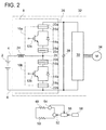
- FIG. 2 shows an electric power conversion equipment, a bidirectional converter and joint layers in an electric automobile.
- a bidirectional converter 8 comprises two semiconductor devices 10a and 10b and a reactor 24.
- the two semiconductor devices 10a and 10b are the same as each other, and in the present specification, when common matters are described, which the devices 10a and 10b share, alphabet subscripts (i.e., a and b) are omitted.
- Each semiconductor device 10 includes a switching element 12, a diode 14 connected in parallel to the switching element 12 and a pair of electrodes (for example, a high potential electrode 16 and a low potential electrode 18).
- the semiconductor device on one side (the first semiconductor device 10a in the present specification) is connected to a high potential wiring 26 (the wiring to which a voltage obtained by boosting a voltage of a battery 2 is applied).
- the semiconductor device on the other side (the second semiconductor device 10b in the present specification) is connected to a low potential wiring 6 (the wiring which is connected to a low potential terminal of the battery 2).
- the first semiconductor device 10a and the second semiconductor device 10b are connected in series between the high potential wiring 26 and the low potential wiring 6, and a connection point 25 between the first semiconductor device 10a and the second semiconductor device 10b is connected via the reactor 24 and a wiring 4 to a high potential terminal of the battery 2.
- Reference numeral 28 represents a capacitor that smoothes out the voltage of the high potential wiring 26
- reference numeral 30 represents an inverter that performs conversion into drive power supplied to a motor 34 and reference numeral 32 represents an electric power conversion equipment.
- Reference numerals 20 and 22 represent joint layers (for example, solder layers) that are connected to the pair of electrodes 16 and 18.
- the joint layer 20a connects one electrode 16a of the first semiconductor device 10a to the high potential wiring 26.
- the joint layer 22a connects the other electrode 18a of the first semiconductor device 10a to the reactor 24 and the second semiconductor device 10b.
- the joint layer 20b connects one electrode 16b of the second semiconductor device 10b to the reactor 24 and the first semiconductor device 10a.
- the joint layer 22b connects the other electrode 18b of the second semiconductor device 10b to the low potential wiring 6.
- the joint layer 20a is a high potential joint layer of the first semiconductor device 10a, and corresponds to the high potential joint layer in the present specification.
- the joint layer 22b is a low potential joint layer of the second semiconductor device 10b, and corresponds to the low potential joint layer in the present specification. As shown in FIG. 5 , which will be described later, there is a case where both the joint layers 22a and 20b are not present.
- FIGS. 3(1) and 3(2) show directions of current flowing at the power running (at the time of voltage boosting) in which a potential obtained by boosting a potential of the wiring 4 is applied to the high potential wiring 26 by the bidirectional converter 8.
- current flowing from the high potential wiring 26 toward the low potential wiring 6 is referred to as "forward current”
- current flowing from the low potential wiring 6 toward the high potential wiring 26 is referred to as "reverse current”.
- the potential of the low potential wiring 6 can be temporarily increased as compared with the potential of the high potential wiring 26 and the reverse current accordingly flows.
- a magnitude relationship of potentials may be reversed.
- FIG. 3(1) shows a state where the forward current flows through the low potential joint layer 22b
- FIG. 3(2) shows a state where the reverse current flows through the high potential joint layer 20a.
- the state of FIG. 3(1) and the state of FIG. 3(2) are alternately switched.
- FIGS. 3(3) and 3(4) show directions of current flowing at the regeneration (at the time of voltage reduction) in which a voltage obtained by reducing a voltage applied to the high potential wiring 26 is applied to the wiring 4 by the bidirectional converter 8.
- FIG. 3(3) shows a state where the forward current flows through the high potential joint layer 20a
- FIG. 3(4) shows a state where the reverse current flows through the low potential joint layer 22b.
- the state of FIG. 3(3) and the state of FIG. 3(4) are alternately switched.
- the semiconductor device 10 of FIG. 1(1) can configure both the semiconductor device 10a that forms an upper arm of the bidirectional converter 8 and the semiconductor device 10b that forms a lower arm thereof. It is found that the bidirectional converter 8 can be configured even with the semiconductor device 10 ⁇ of FIG. 1(2) that is also bidirectional. It is also found that the bidirectional converter 8 can be configured even with the bidirectional semiconductor device 10 ⁇ of FIG. 1(3) . It is found that in any one of FIGS. 1(1), 1(2) and 1(3) , states where the forward current flows through the joint layers 20, 22, 20a, 22 ⁇ , 20 ⁇ and 22 ⁇ and states where the reverse current flows through the joint layers 20, 22, 20 ⁇ , 22 ⁇ , 20 ⁇ and 22 ⁇ are switched, respectively.
- the progression degree of EM generated in the joint layer is affected by a total amount of current passed and a mobility of ions when current is passed. As the total amount of current passed is increased, the EM progresses, whereas as the mobility of ions is higher, the EM rapidly progresses.
- the mobility of ions mainly depends on the temperature of the joint layer.
- a direction in which ions causing EM move is changed depending on the direction in which current is passed.
- reverse current EM is generated after forward current EM is generated, the forward current EM is cancelled out by the reverse current EM, and the progression index of EM actually generated in the joint layer is accordingly reduced.
- forward current EM is generated after reverse current EM is generated, the reverse current EM is cancelled out by the forward current EM, and the progression index of EM actually generated in the joint layer is accordingly reduced.
- both the forward current EM progression index and the reverse current EM progression index are assumed to have a same positive or negative sign, a difference (imbalance amount) between them indicates the progression index of the EM actually generated in joint layer.
- the electric automobile described in the present specification includes the controller configured to compare the progression index of the EM generated by the forward current in the low potential joint layer 22b (i.e. state 1) with the progression index of the EM generated by the reverse current in the low potential joint layer 22b (i.e. state 4), and when the former is higher than the latter, the temperature of the joint layer during the regeneration is increased, whereas when the latter is higher than the former, the temperature of the joint layer during the power running is increased.
- the large EM is more often generated in the low potential joint layer than in the high potential joint layer.
- the imbalance amount of EM generated in the low potential joint layer can be maintained at a low level, this is extremely effective.
- the imbalance amount of EM generated in the joint layer 20b is equal to the imbalance amount of EM generated in the low potential joint layer 22b.
- the imbalance amount of EM generated in the joint layer 20b is also maintained at a low level.
- An electric vehicle comprises an electric power conversion equipment and a motor connected to the electric power conversion equipment.
- the electric power conversion equipment comprises a bidirectional converter including a voltage boosting function and a voltage reducing function.
- the bidirectional converter comprises a semiconductor device including a circuit in which units are connected in series. Each of the units includes a switching element and a diode connected to the switching element in parallel.
- a high potential electrode of the semiconductor device is connected to a high potential wiring via a high potential joint layer, and a low potential electrode of the semiconductor device is connected to a low potential wiring via a low potential joint layer.
- Current flowing from the high potential wiring to the low potential wiring is denoted as forward current, and current flowing from the low potential wiring to the high potential wiring is denoted as reverse current.
- An electric automobile as in feature 1 where an imbalance amount of EM is generated at a larger degree in the low potential joint layer than in the high potential joint layer may include a controller configured to compare a progression index of the EM generated by the forward current of FIG. 3(1) in the low potential joint layer with the progression index of the EM generated by the reverse current of FIG. 3(4) in the low potential joint layer, and when the former is higher than the latter, a temperature of the joint layer during the regeneration is increased whereas when the latter is higher than the former, the temperature of the joint layer during the power running is increased.
- An electric automobile as in feature 1 where the imbalance amount of EM is generated at a larger degree in the high potential joint layer than in the low potential joint layer may include a controller configured to compare a progression index of the EM generated by the reverse current of FIG. 3(2) in the high potential joint layer with a progression index of the EM generated by the forward current of FIG. 3(3) in the high potential joint layer, and when the former is higher than the latter, the temperature of the joint layer during the regeneration is increased whereas when the latter is higher than the former, the temperature of the joint layer during the power running is increased.
- An electric automobile as in feature 1 where it is impossible to predict a magnitude relationship between the imbalance amounts of the EM generated in the low potential joint layer and the EM generated in the high potential joint layer may cancel out the imbalance amount depending on the joint layer in which an absolute value of the imbalance amount is relatively higher.
- the technology of feature 2 is adopted and the imbalance amount generated in the low potential joint layer is reduced.
- the technology of feature 3 is adopted and the imbalance amount generated in the high potential joint layer is reduced.
- a hybrid automobile that comprises an electric power conversion equipment, a motor connected to the electric power conversion equipment, an engine and a power transfer mechanism that adjusts a transfer distribution of power between the motor, the engine and a drive wheel, during the power running operation, during which an output of the engine is in short, (state 1) a state where forward current flows through a low potential joint layer and (state 2) a state where reverse current flows through a high potential joint layer alternately occur, and during the regeneration operation during which the output of the engine in is excess, (state 3) a state where the forward current flows through the high potential joint layer and (state 4) a state where the reverse current flows through the low potential joint layer alternately occur.
- a hybrid automobile where the imbalance amount of EM is generated at a larger degree in the low potential joint layer than in the high potential joint layer may include a controller configured to compare the progression index of the EM generated by the forward current of FIG. 3(1) in the low potential joint layer with the progression index of the EM generated by the reverse current of FIG. 3(4) in the low potential joint layer.
- the controller increases an output of an engine to raise the frequency of the occurrence of the regeneration.
- the controller reduces the output of the engine to raise the frequency of the occurrence of the power running.
- a hybrid automobile where the imbalance amount of EM is generated at a larger degree in the high potential joint layer than in the low potential joint layer may include a controller configured to compare the progression index of the EM generated by the reverse current of FIG. 3(2) in the high potential joint layer with the progression index of the EM generated by the forward current of FIG. 3(3) in the high potential joint layer.
- the controller increases the output of an engine to raise the frequency of the occurrence of the regeneration.
- the controller reduces the output of the engine to raise the frequency of the occurrence of the power running.
- FIG. 2 shows the battery 2, the electric power conversion equipment 32 and the motor 34 included in an electric automobile.
- the electric automobile travels by rotating unillustrated drive wheels with the motor 34.
- the electric power conversion equipment 32 includes the bidirectional converter 8, the smoothing capacitor 28 and the inverter 30.
- the bidirectional converter 8 boosts the voltage of the battery 2 and applies the boosted voltage to the inverter 30.
- the inverter 30 converts direct current into three-phase alternating current, and supplies it to the motor 34.
- the motor 34 generates power by force applied from the driving wheels to the motor 34.
- Three-phase alternating current generated by the motor 34 is converted by the inverter 30 into direct current, the converted voltage is reduced by the bidirectional converter 8 and the reduced voltage charges the battery 2.
- the bidirectional converter 8 includes the reactor 24, the semiconductor device 10a and the semiconductor device 10b.
- the semiconductor devices 10a and 10b are the same as each other, and in the following discussion, a description regarding the devices 10a and 10b will be given as one same semiconductor device, with the subscripts (a, b) omitted.
- the semiconductor device 10 includes the switching element 12 and the diode 14 connected in parallel to the switching element 12.
- the switching element 12 switches current flowing from a high potential wiring 26 side toward a low potential wiring 6 side, and current flowing from the low potential wiring 6 side toward the high potential wiring 26 side cannot flow through the switching element 12.
- the current flowing from the low potential wiring 6 side toward the high potential wiring 26 side flows through the diode 14.
- the switching element 12 and the diode 14 are connected in parallel in opposite directions. Since the reactor 24 is present, current can transiently flow from the low potential wiring 6 side toward the the high potential wiring 26 side.
- the semiconductor device 10 (10a, 10b) includes the high potential electrode 16 (16a, 16b) and the low potential electrode 18 (18a, 18b).
- the high potential electrode 16a of the semiconductor device 10a is mechanically and electrically joined with the high potential joint layer 20a to the high potential wiring 26.
- the low potential electrode 18b of the semiconductor device 10b is mechanically and electrically joined with the low potential joint layer 22b to the low potential wiring 6.
- the low potential electrode 18a of the semiconductor device 10a is mechanically and electrically joined with the high potential side intermediate joint layer 22a to the reactor 24 and the semiconductor device 10b.
- the high potential electrode 16b of the semiconductor device 10b is mechanically and electrically joined with the low potential intermediate joint layer 20b to the reactor 24 and the semiconductor device 10a.
- Reference numeral 4 represents a wiring connected to the high potential terminal of the battery 2
- reference numeral 6 represents a low potential wiring
- reference numeral 26 represents the high potential wiring 26.
- FIGS. 3(1) and 3(2) show current paths along which current flows at the time of power running (at the time of voltage boosting).
- the forward current flows through the low potential joint layer 22b and the low potential side intermediate joint layer 20b
- the reverse current flows through the high potential joint layer 20a and the high potential side intermediate joint layer 22a.
- Situations as illustrated in FIGS. 3(1) and 3(2) alternately occur in power running.
- FIGS. 3(3) and 3(4) show current paths along which current flows at the time of regeneration (at the time of voltage reduction).
- the forward current flows through the high potential joint layer 20a and the high potential side intermediate joint layer 22a
- the reverse current flows through the low potential joint layer 22b and the low potential side intermediate joint layer 20b.
- Situations as illustrated in FIGS. 3(3) and 3(4) alternately occur in regeneration.
- An example that will be described below handles a case where a magnitude relationship between a magnitude of the imbalance amount of EM generated in the high potential joint layer 20a and a magnitude of the imbalance amount of EM generated in the low potential joint layer 22b is unknown and where it is unknown in which one of the high potential joint layer 20a and the low potential joint layer 22b a larger imbalance amount of EM is generated.
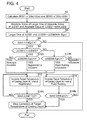
- FIG. 4 shows a control procedure cancelling out an imbalance amount of EM, i.e. for reducing the imbalance amount of EM generated in the joint layer or preventing the magnitude of the imbalance amount of EM from reaching an excessive level, in the electric automobile.
- the control procedure of FIG. 4 can be carried out by a controller (including a calculator) as denoted by reference numeral 58 in FIG. 2 .
- step S2 an index ⁇ EM1 that indicates the magnitude of the imbalance amount of EM generated in the high potential joint layer 20a and an index ⁇ EM2 that indicates the magnitude of the imbalance amount of EM generated in the low potential joint layer 22b are calculated.
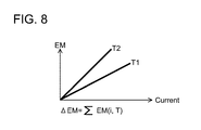
- the progression rate is changed depending on the temperature of the joint layer when current is passed. Specifically, when the temperature is a higher temperature (T2), the progression rate is larger whereas when the temperature is a lower temperature (T1), the progression rate is smaller.
- the electric automobile of the example collects, over time, data indicating the value of current passed and the temperature of the joint layer at that time, and has a function of calculating the progression index of EM in the joint layer. For example, in a two-dimensional map in which the horizontal axis represents the current value and the vertical axis represents the temperature of the joint layer, values indicating the progression rates of EM are stored. This map can be prepared in advance by actually measuring the current values, the temperatures and the progression rates of EM. The progression rates EM (i, T) corresponding to the current values and the temperatures are read and integrated over time, and thus the progression index of EM can be calculated. Both the progression index of EM caused by the forward current and the progression index of EM caused by the reverse current are calculated as having positive values.
- a progression index ⁇ EM indicating the magnitude of the imbalance amount of EM is calculated by the difference between the progression index of EM caused by the forward current and the progression index of EM caused by the reverse current.
- ⁇ EM is a positive value.
- step S4 of FIG. 4 an absolute value of ⁇ EM1 is compared with an absolute value of ⁇ EM2, and a larger absolute value is assumed to be MAX ⁇ EM.
- step S6 ⁇ EM (with positive or negative sign) having a larger absolute value between ⁇ EM1 and ⁇ EM2 is assumed to be ⁇ EM (with sign).
- step S8 the MAX ⁇ EM is compared with an allowable value C1.
- the allowable value C1 indicates an allowable value for the imbalance amount of EM, and when MAX ⁇ EM ⁇ C1, this case corresponds to a case where it is not necessary to perform control for the reduction of the imbalance amount of EM.
- MAX ⁇ EM ⁇ C1 No in step S8, the process does not proceed to processing in step S9 and subsequent steps.
- step S8 the magnitude of the imbalance amount of EM is larger than the allowable value C1, and this case corresponds to a case where it is necessary to perform control for the reduction of the imbalance amount of EM.
- step S9 the magnitude relationship between the absolute value of ⁇ EM1 and the absolute value of ⁇ EM2 is determined. That is, the magnitude of the imbalance amount of EM generated in the high potential joint layer 20a is compared with the magnitude of the imbalance amount of EM generated in the low potential joint layer 22b. Then, in step S10A/B, it is determined whether the ⁇ EM (with sign) is positive or negative.
- step S12 the target temperature of a cooling liquid at the time of regeneration is increased so as to increase the temperature of the joint layers.
- the semiconductor devices 10, the joint layers 20 and 22 and the like are cooled with the cooling liquid.
- reference numeral 48 represents a heat exchanger that exchanges heat between the semiconductor devices 10 (the joint layers 20, 22 and the like) and the cooling liquid.
- Reference numeral 50 represents a heat exchanger that exchanges heat between the cooling liquid and the atmosphere.
- Reference numeral 52 represents a cooling liquid pump. The cooling liquid is circulated by the pump 52, cools down the joint layers 20 and 22 while being heated there, and is cooled by the heat exchanger 50. The cooling liquid repeats this circulation.
- Reference numeral 54 represents a temperature sensor that detects a temperature of the cooling liquid, and a pump control device 56 performs feed-back control on a number of revolutions of the pump 52 to maintain the temperature of the cooling liquid at a target temperature.
- Reference numeral 58 represents a control device that has a function of calculating the forward current EM progression index, the reverse current EM progression index and the imbalance EM progression index and that performs the control procedure of FIG. 4 .
- step S12 the regeneration operation is performed in an environment in which the temperature of the joint layers 20 and 22 is high, and the power running operation is performed in an environment in which the temperature of the joint layers 20 and 22 is low.
- the EM rapidly progresses.
- step S12 is performed, as a result, in the regeneration operation following step S12, the imbalance amount of EM is reduced.
- step S14 the target temperature of the cooling liquid at the time of power running is increased so as to increase the temperature of the joint layers.
- the power running operation is performed in the environment in which the temperature of the joint layers 20 and 22 is high, and the regeneration operation is performed in the environment in which the temperature of the joint layers 20 and 22 is low.
- the EM rapidly progresses.
- step S 14 is performed, as a result, in the power running operation following step S 14, the imbalance amount of EM is reduced.
- step S16A YES is selected.
- C2 used in step S16A is sufficiently lower than the allowable value C1 used in step S8, and is such a small value by which it can be determined that the imbalance amount of EM bas become sufficiently low and that the processing for cancelling out the imbalance amount bas become unnecessary.
- NO is selected in step S16A, the processing in step S12 is continuously performed, and when it is determined in step S16A that the imbalance amount has been cancelled out, step S18 is performed to complete the processing for cancelling out the imbalance amount.
- step S16B YES is selected.
- C2 used in step S16B is sufficiently lower than the allowable value C1 used in step S8 and is such a small value by which it can be determined that the imbalance amount of EM has become sufficiently low and that the processing for cancelling out the imbalance amount has become unnecessary.
- NO is selected in step S16B, the processing in step S14 is continuously performed, and when it is determined in step S16B that the imbalance amount has been cancelled out, step S18 is performed to complete the processing for cancelling out the imbalance amount.
- the processing of FIG. 4 handles a case where a magnitude relationship between the imbalance amount of EM generated in the high potential joint layer 20a and the imbalance amount of EM generated in the low potential joint layer 22b is unknown.
- the processing of FIG. 4 corresponds to the technology of feature 4.
- step S8 to step S10B the technology of feature 2 corresponds to this case.
- imbalance amount of EM generated in the high potential joint layer 20a is larger than the imbalance amount of EM generated in the low potential joint layer 22b, and in that case, whether the power running or the regeneration is excessive may be determined depending on the high potential joint layer 20a having the larger imbalance amount.
- step S9 of FIG. 4 since the determination in step S9 of FIG. 4 is not needed, and the process may proceed from step S8 to step S10A, the technology of feature 3 corresponds to this case.
- the EM generated in the high potential joint layer 20a and the EM generated in the high potential side intermediate joint layer 22a are the same. Therefore, by performing processing for suppressing the EM generated in the high potential joint layer 20a, the imbalance amount of EM generated in the high potential side intermediate joint layer 22a is also suppressed.
- the EM generated in the low potential joint layer 22b and the EM generated in the low potential side intermediate joint layer 20b are the same. Therefore, by performing processing for suppressing the EM generated in the low potential joint layer 22b, the imbalance amount of EM generated in the low potential side intermediate joint layer 20b is also suppressed.
- the technology described in the example is not limited only to this example.
- the technology described in the example can be alternatively applied to a case where one semiconductor device is joined with two joint layers as shown in FIGS. 1(1) and 1(2) .
- same imbalance amounts of EM are generated in the two joint layers, and by performing the processing for cancelling out the imbalance amount of EM, both the imbalance amounts of EM in the two joint layers are commonly reduced.
- the processing procedure of FIG. 4 is simplified. Whether the power running or the regeneration is excessive can be determined by focusing on either one of the joint layers, and step S12 or step S14 can be selected by that determination result.
- the technology is also useful for a case where the bidirectional converter is configured of one semiconductor device without the presence of the high potential side intermediate joint layer 22a and the low potential side intermediate joint layer 20b.
- EM may also be generated in a reactor joint layer 38 with which a reactor 24 and a semiconductor device 10 are joined.
- a direction of current flowing through the reactor joint layer 38 is reversed depending on whether the power running is performed or the regeneration is performed.
- the imbalance amount of EM can be reduced by performing step S12 in FIG. 4 .
- the imbalance amount of EM generated in the reactor joint layer 38 can be reduced by performing step S14 of FIG. 4 .
- step S4 of FIG. 4 may be modified to a processing in which a maximum absolute value among the imbalance amounts of EM in the high potential joint layer 20, the low potential joint layer 22 and the reactor joint layer 38 is focused on.
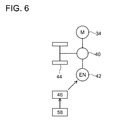
- a hybrid automobile includes an engine 42 in addition to the motor 34, and also includes a power distribution mechanism 40 that adjusts transmission distribution of power between the motor 34, the engine 42 and drive wheels 44.
- the motor 34 performs the power running operation to apply the necessary power to the drive wheels 44.
- the motor 34 performs the regeneration operation to generate power.
- Reference numeral 46 represents a device for adjusting the engine output
- reference numeral 58 represents a computer device that has a function of calculating the forward current EM progression index, the reverse current EM progression index and the imbalance EM progression index and is a controller for performing the control procedure of FIG. 7 .
- FIG. 7 is a control procedure cancelling out an imbalance amount of EM, i.e. for reducing the imbalance amount of EM generated in the joint layer or preventing the magnitude of the imbalance amount of EM from reaching an excessive level, in the hybrid automobile.
- the control procedure of FIG. 7 can be carried out by a controller (including a calculator) as denoted by reference numeral 58 in FIG. 6 . It is similar to the processing procedure of FIG. 4 , and thus description thereof that is common to FIG. 4 will not be repeated.
- steps 10A and 10B of FIG. 7 With processing until steps 10A and 10B of FIG. 7 , whether the power running is excessive or the regeneration is excessive is determined for the joint layer whose imbalance amount of EM is larger than the allowable value C1. The processing is the same as the processing of FIG. 4 until then.
- step S12a When the power running is excessive, a correction for increasing the engine output is performed in step S12a. Then, a frequency at which the motor 34 performs the regeneration operation is increased. It is possible to obtain a phenomenon in which the imbalance amount of EM generated by the excessive power running is shrunk by the regeneration operation.
- step S14a When the regeneration is excessive, a correction for reducing the engine output is performed in step S14a. Then, a frequency at which the motor 34 performs the power running operation is increased. It is possible to obtain a phenomenon in which the imbalance amount of EM generated by the excessive regeneration is shrunk by the power running operation.
- step S8 when it is found that the imbalance amount of EM generated in the low potential joint layer 22b is larger than the imbalance amount of EM generated in the high potential joint layer 20a, whether the power running or the regeneration is excessive may be determined depending on the low potential joint layer 22b having the larger imbalance amount.
- step S9 when YES is selected in step S8, step S9 may be omitted to proceed to a determination in step S10B.
- the technology of feature 6 corresponds to this case.
- the imbalance amount of EM generated in the high potential joint layer 20a is larger than the imbalance amount of EM generated in the low potential joint layer 22b
- whether the power running or the regeneration is excessive may be determined depending on the high potential joint layer 20a having the larger imbalance amount.
- step S9 may be omitted to proceed to a determination in step S10A.
- the technology of feature 7 corresponds to this case.
- the processing of FIG. 7 illustrates a technology that copes with the case where the magnitude relationship between the imbalance amount of EM generated in the high potential joint layer 20a and the imbalance amount of EM generated in the low potential joint layer 22b is unknown, and corresponds to the technology of feature 8.
- FIGS. 4 and 7 can be merged for a hybrid automobile.
- step S12a but also step S12 of FIG. 4 can also be performed.
- step S14a but also step S14 of FIG. 4 can also be performed.
- step S12, steps S12 and S12a or only step S12a may be performed.
- steps S 14 and S 14a or only step S 14a may be performed.
- the IGBT is utilized as the switching element, as an example.
- a MOS may be alternatively used, for example.
- the present technology can also be applied to a converter utilizing a MOS that performs a synchronous rectification operation.
- the present technology can also be applied to a converter utilizing a MOS incorporating a diode.
- an electronic equipment is provided with a semiconductor device including an electrode joined to an electric conductor via a joint layer, a calculator and a controller.
- the semiconductor device is configured to pass current bidirectionally.
- the calculator is configured to calculate an imbalance electromigration (EM) progression index.
- the imbalance EM progression index is a difference between a forward current EM progression index and a reverse current EM progression index.
- the controller is configured to: adopt a condition to speed up an increase rate of the reverse current EM progression index in at least a part of an excessive forward current EM period; and adopt a condition to speed up an increase rate of the forward current EM progression index in at least a part of an excessive reverse current EM period.
Landscapes
- Engineering & Computer Science (AREA)
- Life Sciences & Earth Sciences (AREA)
- Sustainable Development (AREA)
- Sustainable Energy (AREA)
- Power Engineering (AREA)
- Transportation (AREA)
- Mechanical Engineering (AREA)
- Electric Propulsion And Braking For Vehicles (AREA)
- Dc-Dc Converters (AREA)
- Hybrid Electric Vehicles (AREA)
- Inverter Devices (AREA)
Abstract
Description
- The present specification discloses an electronic equipment in which a semiconductor device having an electrode exposed on a surface of the semiconductor device is joined to an electric conductor via a joint layer, and also discloses an automobile on which the electronic equipment is mounted.
- A semiconductor device including an electrode exposed on a surface of the semiconductor device is used under a state where the electrode is joined to an electric conductor via a joint layer. Current flows through the joint layer. When current flows through the joint layer, a phenomenon occurs in which ions in the joint layer are moved. In the present specification, this phenomenon is called electromigration, and may be abbreviated as EM. Progression of EM leads to occurrence of a defect in the joint layer, and thus results in unstable operation of the semiconductor device or an electronic equipment including the semiconductor device. Japanese Patent Application Publication No.
2013-175578 2013-175578 - In the technology of adding the metal layer, an extra metal layer is needed, and this causes costs to be increased. Moreover, the technology needs a lot of processes since it is necessary to change a type of metal depending on a direction along which current is passed.
- With regard to the above, an object of the present specification is to provide a technology that suppresses the progression of EM without the addition of a metal layer.
- In order to achieve this object, the present specification discloses an electronic equipment and various vehicles including such electronic equipment, as defined in the claims. Features, advantages, and technical and industrial significance of exemplary embodiments of the present specification will be described below with reference to the accompanying drawings.
- In the electronic equipment disclosed in the present specification, a semiconductor device passes current bidirectionally, and a direction of current is switched over time between a state in which forward current flows through a joint layer and a state in which reverse current flows through the joint layer.
-
-
FIGS. 1(1) to 1(3) show examples of circuit configurations of a semiconductor device; -
FIG. 2 shows an electric power conversion equipment, a bidirectional converter and joint layers in an electric automobile; -
FIGS. 3(1) to 3(4) show directions of current flowing through the joint layers; -
FIG. 4 shows a control procedure for cancelling out an imbalance amount of EM in the electric automobile; -
FIG. 5 shows a case where one semiconductor device incorporates a circuit in which a pair of units are connected in series and each of the units includes a switching element and a diode connected in parallel to the switching element; -
FIG. 6 shows a drive mechanism of a hybrid automobile; -
FIG. 7 shows a control procedure for cancelling an imbalance amount of EM in the hybrid automobile; and -
FIG. 8 schematically shows a relationship between a degree of progression of EM, a current value and a temperature. - The technology described in the present specification is useful for an electric automobile which includes a motor and a drive wheel and travels by rotating the drive wheel with the motor. The "electric automobile" described here includes an electric automobile in which power is supplied from a battery to a motor, a fuel battery automobile in which power is supplied from a fuel battery to a motor, an automobile in which power is supplied from a generator driven by an engine to a motor, and a hybrid automobile which includes an engine in addition to a motor and in which a drive wheel is rotated by the motor and/or the engine.
- The electric automobile in which the drive wheel is driven by the motor includes an electric power conversion equipment that is connected to the motor. Among electric automobiles, an automobile is known which includes a bidirectional converter, having both a voltage boosting function and a voltage reducing function, boosts a battery voltage, supplies the boosted voltage to a motor, reduces a voltage generated by the motor operating as a generator and charges the battery by the reduced voltage. The bidirectional converter is part of the electric power conversion equipment. In the present specification, a case where power is supplied to the motor to rotate the drive wheel is referred to as "power running" or "power running operation", and a case where the drive wheel applies torque to the motor and thus the motor generates power is referred to as "regeneration" or "regeneration operation". The electric power conversion equipment at the time of power running boosts a battery voltage to convert it into a motor drive current, and the electric power conversion equipment at the time of regeneration converts power generated by the motor into a charge current of the battery. Although the motor in this context may be referred to as a "motor generator" by focusing attention on the fact that the motor serves as a motor or a generator, in the present specification the motor is simply referred to as a motor. In a case of a hybrid automobile, a motor or both the motor and the drive wheel can be rotated by an engine. This is also the regeneration.
- Before describing specific exemplary embodiments, the basic principles of the technology of the present specification are outlined below.
- In the electronic equipment disclosed in the present specification, a semiconductor device passes current bidirectionally, and a direction of current is switched over time between a state in which forward current flows through a joint layer and a state in which reverse current flows through the joint layer.
- For example, in a
semiconductor device 10 shown inFIG. 1(1) , anIGBT 12 and adiode 14 are connected in parallel, and a highpotential electrode 16 and alow potential electrode 18 are exposed on a surface of thesemiconductor device 10, respectively. The highpotential electrode 16 is connected via a highpotential joint layer 20 to an unillustrated high potential electric conductor, and thelow potential electrode 18 is connected via a lowpotential joint layer 22 to an unillustrated low potential electric conductor. Thesemiconductor device 10 is bidirectional, and in thesemiconductor device 10, as shown by arrows (a), current may flow from the highpotential electrode 16 toward thelow potential electrode 18 via theIGBT 12, or as shown by arrows (b), current may flow from thelow potential electrode 18 toward the highpotential electrode 16 via thediode 14. In a transient state or the like, a potential of thelow potential electrode 18 may be temporarily higher than that of the highpotential electrode 16, and thus reverse current may flow. In the present specification, the current flowing from the highpotential electrode 16 toward thelow potential electrode 18 is referred to as forward current, and the current flowing from thelow potential electrode 18 toward the highpotential electrode 16 in a transient state or the like is referred to as reverse current. Thesemiconductor device 10 ofFIG. 1(1) passes current bidirectionally, and the direction of the current is switched over time between a state in which the forward current flows and a state in which the reverse current flows. Accordingly, the direction of the current is switched over time between a state where the forward current flows through thejoint layers joint layers - The electronic equipment disclosed in the present specification comprises a calculator and a controller. The calculator is configured to calculate an imbalance EM progression index. The imbalance EM progression index is a difference between a progression index (in the present specification, referred to as a forward current EM progression index) of EM generated in the joint layer due to the flowing of the forward current through the joint layer and a progression index (referred to as a reverse current EM progression index) of EM generated in the joint layer due to the flowing of the reverse current through the joint layer. The controller is configured to cause phenomena that suppress the progression of the EM by cancelling out the forward current EM with the reverse current EM and alternatively by cancelling out the reverse current EM with the forward current EM. The controller is configured to (adopt a condition to) speed up an increase rate of the reverse current EM progression index in at least a part of an excessive forward current EM period during which the forward current EM progression index is larger than the reverse current EM progression index. Also, the controller is configured to (adopt a condition to) speed up an increase rate of the forward current EM progression index in at least a part of an excessive reverse current EM period during which the reverse current EM progression index is larger than the forward current EM progression index.
- In a case of
FIG. 1(1) , while the forward current shown by arrows (a) is passed, the forward current EM progresses in thejoint layers 20 and 22 (that is, there occurs a forward current EM progression with a certain forward current EM progression index, rate or degree indicating a (temporal) increase amount of forward current EM progression), and while the reverse current shown by arrows (b) is passed, the reverse current EM progresses in thejoint layers joint layers joint layers joint layers - When the progression index (the forward current EM progression index) of the EM generated in the joint layer due to the flow of the forward current through the joint layer is larger than the progression index (the reverse current EM progression index) of the EM generated in the joint layer due to the flow of the reverse current through the joint layer, it can be said that the forward current EM is excessive. In this case, the controller is configured to (adopt the condition to) speed up the increase rate of the reverse current EM progression index. Thus, when the EM caused by the forward current is excessive, thereafter the controller is configured to (adopt the condition to) speed up the increase rate of the progression index of the EM caused by the reverse current. Hence, the excessive EM generated by the forward current is cancelled out by the subsequent reverse current, and thereby the imbalance amount of EM is reduced.
- By contrast, when the forward current EM progression index is smaller than the reverse current EM progression index, it can be said that the reverse current EM is excessive. In this case, the controller is configured to (adopt the condition to) speed up the increase rate of the forward current EM progression index. Hence, the excessive EM generated by the reverse current is cancelled out by the subsequent forward current, and thereby the imbalance amount of EM is reduced.
- With the technology described above, it is possible to suppress the EM that actually is being generated (the imbalance amount of the forward current EM and the reverse current EM = an absolute value of a difference between the forward current EM progression index and the reverse current EM progression index) from developing to be a large absolute value.
- In the case of
FIG. 1(1) , since a current of a same intensity flows in a same direction through thejoint layer 20 and thejoint layer 22, it can be assumed that the EM generated in thejoint layer 20 is the same as the EM generated in thejoint layer 22. When attention is focused on the imbalance amount of EM generated in thejoint layer 20 and the imbalance amount of EM generated in thejoint layer 20 is controlled so as to be reduced, the imbalance amount of EM generated in thejoint layer 22 is also reduced. Likewise, when attention is focused on the imbalance amount of EM generated in thejoint layer 22 and the imbalance amount of EM generated in thejoint layer 22 is controlled so as to be reduced, the imbalance amount of EM generated in thejoint layer 20 is also reduced. In the technology described in the present specification, in a case where a plurality of joint layers are present, an advantageous effect may thus be obtained even by applying the technology to one of the joint layers. In a case where a semiconductor device is joined to an electric conductor via a plurality of joint layers, a technology of the present specification need not be applied to all the joint layers, and the advantageous effect may also be obtained by applying the technology to one of the joint layers. - The
semiconductor device 10 ofFIG. 1(1) is simply an example, and may not be limited to this example. For example,FIG. 1(2) shows a semiconductor device 10α that incorporates a MOS, and even in the semiconductor device 10α, a direction of current is switched over time between a state in which forward current flows through joint layers 20α and 22α and a state in which a reverse current flows through joint layers 20α and 22α. The technology described in the present specification is also useful for the semiconductor device shown inFIG. 1(2) . - In a case of a semiconductor device 10β of
FIG. 1(3) , parallel circuits, each formed of anIGBT 12 and adiode 14, are connected in series. Even in this device, a direction of current is switched over time between a state in which forward current flows through joint layers 20β and 22β and a state in which reverse current flows through the joint layers 20β and 22β. As will be described in detail later, in the case ofFIG. 1(3) , the direction of the current is switched over time among a direction shown by an arrow (a2) indicating a state where the forward current flows through the joint layer 22β, a direction shown by an arrow (b1) indicating a state where the reverse current flows through the joint layer 20β, a direction shown by an arrow (a1) indicating a state where the forward current flows through the joint layer 20β and a direction shown by an arrow (b2) indicating a state where the reverse current flows through the joint layer 22β. In this case, the state where the forward current flows through the joint layer 20β and the state where the forward current flows through the joint layer 22β occur at different times, and the state where the reverse current flows through the joint layer 20β and the state where the reverse current flows through the joint layer 22β occur at different times. A magnitude of the current flowing through the joint layer 20β differs from a magnitude of the current flowing through the joint layer 22β. The technology described in the present specification can be applied to the semiconductor device shown inFIG. 1(3) , that is, the equipment having two or more joint layers 20β and 22β that differ in the direction of the current being passed and a value of the current being passed. As will be described later, the technology can also be applied to an electronic equipment that has three or more joint layers 20β, 22β and 38β. As indicated above, the semiconductor device 10β ofFIG. 1(3), FIG. 1(2) can equally incorporate a MOS in each of the parallel circuits as well. - The semiconductor devices shown in
FIGS. 1(1) and 1(2) may form an upper arm or a lower arm in a bidirectional converter (having both a voltage boosting function and a voltage reducing function) mounted on an electric automobile. The semiconductor device shown inFIG. 1(3) may form a bidirectional converter mounted on an electric automobile. The technology described in the present specification can be applied to any joint layer via which a semiconductor device configuring a bidirectional converter mounted on an electric automobile is joined to an electric conductor. - The controller may increase a temperature of the joint layer when the reverse current flows in the at least part of the excessive forward current EM period, and may increase the temperature of the joint layer when the forward current flows in the at least part of the excessive reverse current EM period. When the temperature of the joint layer is increased, the progression rate of the EM is increased. In other words, the increase rate of the progression index of the EM is speeded up. When the temperature of the joint layer is increased when the reverse current flows in the excessive forward current EM period, the increase rate of the progression index of the EM caused by the reverse current is speeded up. Therefore, the imbalance amount in which the forward current EM is excessive is reduced while the reverse current is being passed. As a result, the EM actually being generated in the joint layer is reduced. Likewise, when the temperature of the joint layer is increased when the forward current flows in the excessive reverse current EM period, the increase rate of the progression index of the EM caused by the forward current is speeded up. Therefore, the imbalance amount in which the reverse current EM is excessive is reduced while the forward current is being passed. As a result, the EM actually being generated in the joint layer is reduced.
- The controller may increase occasions at which the reverse current flows during the excessive forward current EM period, and may increase occasions at which the forward current flows during the excessive reverse current EM period. As will be described in detail later, there is a case where adjusting a voltage supplied to an electronic equipment may allow to control whether the forward current or the reverse current flows through the semiconductor device. When such control can be performed, the occasions at which the reverse current flows can be increased during the excessive forward current EM period, and thus it is possible to reduce the imbalance amount of EM generated in the joint layer, and the occasions at which the forward current flows can be increased during the excessive reverse current EM period, and thus it is possible to reduce the imbalance amount of EM generated in the joint layer.
- In a case where the forward current and the reverse current alternately flow within a predetermined time, the increasing of the occasions at which the forward current flows leads to raising a degree of increase in the progression index of EM caused by the forward current within the predetermined time. The increasing of the temperature of the joint layer when the forward current is passed and/or the increasing of the occasions at which the forward current flows are equivalent to adopting or switching to the condition to speed up the increase rate of the progression index of the EM caused by the forward current. In order to achieve the speeding up, both the increasing of the temperature of the joint layer and the increasing of the occasions at which the forward current flows may be implemented together. Likewise, the increasing of the temperature of the joint layer when the reverse current is passed and/or the increasing of the occasions at which the reverse current flows are equivalent to adopting or switching to the condition to speed up the increase rate of the progression index of the EM caused by the reverse current. Both the increasing of the temperature of the joint layer and the increasing of the occasions at which the reverse current flows may be implemented together.
- When a condition to speed up the increase rate of the progression index of the EM caused by the reverse current is adopted in the excessive forward current EM period, the progression index of the EM generated by the reverse current in the joint layer is increased. As a result, the progression index of the EM generated by the forward current in the joint layer and the progression index of the EM generated by the reverse current in the joint layer are balanced. By contrast, when a condition to speed up the increase rate of the progression index of the EM caused by the forward current is adopted in the excessive reverse current EM period, the progression index of the EM generated by the forward current in the joint layer is increased. As a result, the progression index of the EM generated by the forward current in the joint layer and the progression index of the EM generated by the reverse current in the joint layer are balanced. When both of the progression indices are balanced, the adoption of any one of the conditions to speed up the respective increase rate may be stopped.
- What is meant by "the forward current EM progression index is larger than the reverse current EM progression index" is that a difference obtained by subtracting the reverse current EM progression index from the forward current EM progression index is a first predetermined value or more. What is meant by "the reverse current EM progression index is larger than the forward current EM progression index" is that a difference obtained by subtracting the forward current EM progression index from the reverse current EM progression index is the first predetermined value or more. What is meant by "the forward current EM progression index and the reverse current EM progression index are balanced" is that the absolute value of a difference between the forward current EM progression index and the reverse current EM progression index is (reduced to) a second predetermined value or less. A relationship is set such that the first predetermined value is smaller than the second predetermined value. When the absolute value of the imbalance amount of EM is or reaches the first predetermined value or more, processing for cancelling out the imbalance is performed, whereas when the absolute value of the imbalance amount of EM is or reaches the second predetermined value or less, the processing for cancelling out the imbalance is terminated. A magnitude of the imbalance amount of EM refers to the absolute value of the difference (imbalance EM progression index) between the forward current EM progression index and the reverse current EM progression index. The cancelling out of the imbalance amount of EM means reducing the absolute value of the difference.
-
FIG. 2 shows an electric power conversion equipment, a bidirectional converter and joint layers in an electric automobile. As shown inFig. 2 , a technology is known in which abidirectional converter 8 comprises twosemiconductor devices reactor 24. The twosemiconductor devices devices semiconductor device 10 includes a switchingelement 12, adiode 14 connected in parallel to the switchingelement 12 and a pair of electrodes (for example, a highpotential electrode 16 and a low potential electrode 18). - The semiconductor device on one side (the
first semiconductor device 10a in the present specification) is connected to a high potential wiring 26 (the wiring to which a voltage obtained by boosting a voltage of abattery 2 is applied). The semiconductor device on the other side (thesecond semiconductor device 10b in the present specification) is connected to a low potential wiring 6 (the wiring which is connected to a low potential terminal of the battery 2). Thefirst semiconductor device 10a and thesecond semiconductor device 10b are connected in series between the highpotential wiring 26 and the lowpotential wiring 6, and aconnection point 25 between thefirst semiconductor device 10a and thesecond semiconductor device 10b is connected via thereactor 24 and awiring 4 to a high potential terminal of thebattery 2.Reference numeral 28 represents a capacitor that smoothes out the voltage of the highpotential wiring 26,reference numeral 30 represents an inverter that performs conversion into drive power supplied to amotor 34 andreference numeral 32 represents an electric power conversion equipment. -
Reference numerals electrodes joint layer 20a connects oneelectrode 16a of thefirst semiconductor device 10a to the highpotential wiring 26. Thejoint layer 22a connects theother electrode 18a of thefirst semiconductor device 10a to thereactor 24 and thesecond semiconductor device 10b. Thejoint layer 20b connects oneelectrode 16b of thesecond semiconductor device 10b to thereactor 24 and thefirst semiconductor device 10a. Thejoint layer 22b connects theother electrode 18b of thesecond semiconductor device 10b to the lowpotential wiring 6. - The
joint layer 20a is a high potential joint layer of thefirst semiconductor device 10a, and corresponds to the high potential joint layer in the present specification. Thejoint layer 22b is a low potential joint layer of thesecond semiconductor device 10b, and corresponds to the low potential joint layer in the present specification. As shown inFIG. 5 , which will be described later, there is a case where both thejoint layers -
FIGS. 3(1) and 3(2) show directions of current flowing at the power running (at the time of voltage boosting) in which a potential obtained by boosting a potential of thewiring 4 is applied to the highpotential wiring 26 by thebidirectional converter 8. In the present specification, current flowing from the highpotential wiring 26 toward the lowpotential wiring 6 is referred to as "forward current", and current flowing from the lowpotential wiring 6 toward the highpotential wiring 26 is referred to as "reverse current". In a transient period, which will be described later, due to the presence of thereactor 24, the potential of the lowpotential wiring 6 can be temporarily increased as compared with the potential of the highpotential wiring 26 and the reverse current accordingly flows. In the transient period, a magnitude relationship of potentials may be reversed. -
FIG. 3(1) shows a state where the forward current flows through the low potentialjoint layer 22b, andFIG. 3(2) shows a state where the reverse current flows through the high potentialjoint layer 20a. At the time of power running, the state ofFIG. 3(1) and the state ofFIG. 3(2) are alternately switched. -
FIGS. 3(3) and 3(4) show directions of current flowing at the regeneration (at the time of voltage reduction) in which a voltage obtained by reducing a voltage applied to the highpotential wiring 26 is applied to thewiring 4 by thebidirectional converter 8. -
FIG. 3(3) shows a state where the forward current flows through the high potentialjoint layer 20a, andFIG. 3(4) shows a state where the reverse current flows through the low potentialjoint layer 22b. At the time of regeneration, the state ofFIG. 3(3) and the state ofFIG. 3(4) are alternately switched. - It is found that the
semiconductor device 10 ofFIG. 1(1) can configure both thesemiconductor device 10a that forms an upper arm of thebidirectional converter 8 and thesemiconductor device 10b that forms a lower arm thereof. It is found that thebidirectional converter 8 can be configured even with the semiconductor device 10α ofFIG. 1(2) that is also bidirectional. It is also found that thebidirectional converter 8 can be configured even with the bidirectional semiconductor device 10β ofFIG. 1(3) . It is found that in any one ofFIGS. 1(1), 1(2) and 1(3) , states where the forward current flows through thejoint layers joint layers - In the following, the technology of the present specification is described when being applied to a converter of an electric automobile. In a case of the electric power conversion equipment described below, as shown in
FIG. 3 , following two states alternately occur at the time of power running: (state 1) a state where forward current flows through a low potential joint layer and (state 2) a state where reverse current flows through a high potential joint layer, and following two states alternately occur at the time of regeneration: (state 3) a state where the forward current flows through the high potential joint layer, and (state 4) a state where the reverse current flows through the low potential joint layer. - The progression degree of EM generated in the joint layer is affected by a total amount of current passed and a mobility of ions when current is passed. As the total amount of current passed is increased, the EM progresses, whereas as the mobility of ions is higher, the EM rapidly progresses. The mobility of ions mainly depends on the temperature of the joint layer. By collecting over time, data indicating the current passed and the temperature of the joint layer at that timing, an index indicating the progression degree of EM can be calculated. The electric automobile disclosed in the present specification has a function of collecting, over time, data indicating a magnitude of the current passed and the temperature of the joint layer at that time to calculate the progression index of EM.
- A direction in which ions causing EM move is changed depending on the direction in which current is passed. When reverse current EM is generated after forward current EM is generated, the forward current EM is cancelled out by the reverse current EM, and the progression index of EM actually generated in the joint layer is accordingly reduced. Likewise, when forward current EM is generated after reverse current EM is generated, the reverse current EM is cancelled out by the forward current EM, and the progression index of EM actually generated in the joint layer is accordingly reduced. When both the forward current EM progression index and the reverse current EM progression index are assumed to have a same positive or negative sign, a difference (imbalance amount) between them indicates the progression index of the EM actually generated in joint layer.
- In a case of an electric automobile, large EM is more often generated in the low potential
joint layer 22b than in the high potentialjoint layer 20a. If the imbalance amount of EM generated in the low potentialjoint layer 20a can be maintained at a low level, this is extremely effective. Hence, the electric automobile described in the present specification includes the controller configured to compare the progression index of the EM generated by the forward current in the low potentialjoint layer 22b (i.e. state 1) with the progression index of the EM generated by the reverse current in the low potentialjoint layer 22b (i.e. state 4), and when the former is higher than the latter, the temperature of the joint layer during the regeneration is increased, whereas when the latter is higher than the former, the temperature of the joint layer during the power running is increased. - Hence, when the progression index of the EM of the low potential
joint layer 22b generated by the forward current ofFIG. 3(1) at the time of power running is higher than the progression index of the EM of the low potentialjoint layer 22b generated by the reverse current ofFIG. 3(4) at the time of regeneration, the temperature of the joint layer during the regeneration is increased. As a result, the EM is made to rapidly progress in the subsequent regeneration and thus the imbalance amount of EM is cancelled out. By contrast, when the progression index of the EM of the low potentialjoint layer 22b generated by the forward current ofFIG. 3(1) at the time of power running is lower than the progression index of the EM for the low potentialjoint layer 22b generated by the reverse current ofFIG. 3(4) at the time of regeneration, the temperature of the joint layer during the power running is increased. As a result, the EM is made to rapidly progress in the subsequent power running and thus the imbalance amount of EM is cancelled out. In this way, it is possible to maintain the imbalance amount of EM generated in the low potentialjoint layer 22b at a low level. - As described above, in the case of an electric automobile, the large EM is more often generated in the low potential joint layer than in the high potential joint layer. Thus, if the imbalance amount of EM generated in the low potential joint layer can be maintained at a low level, this is extremely effective.
- As described above, the imbalance amount of EM generated in the
joint layer 20b is equal to the imbalance amount of EM generated in the low potentialjoint layer 22b. When a control technology for maintaining the imbalance amount of EM at a low level is adopted to the low potentialjoint layer 22b, the imbalance amount of EM generated in thejoint layer 20b is also maintained at a low level. - The technology described in the present specification can be practiced in various types of aspects, and may have one or more of the following technological features (each including a set of sub-features or properties which are not necessarily linked together but could be (at least partly) separated, as a skilled person would readily understand).
- (Feature 1) An electric vehicle comprises an electric power conversion equipment and a motor connected to the electric power conversion equipment. The electric power conversion equipment comprises a bidirectional converter including a voltage boosting function and a voltage reducing function. The bidirectional converter comprises a semiconductor device including a circuit in which units are connected in series. Each of the units includes a switching element and a diode connected to the switching element in parallel. A high potential electrode of the semiconductor device is connected to a high potential wiring via a high potential joint layer, and a low potential electrode of the semiconductor device is connected to a low potential wiring via a low potential joint layer. Current flowing from the high potential wiring to the low potential wiring is denoted as forward current, and current flowing from the low potential wiring to the high potential wiring is denoted as reverse current. A state in which the forward current flows through the low potential joint layer and a state in which the reverse current flows through the high potential joint layer alternately occur during a power running operation. A state in which the forward current flows through the high potential joint layer and a state in which the reverse current flows through the low potential joint layer alternately occur during a regeneration operation.
- (Feature 2) An electric automobile as in
feature 1 where an imbalance amount of EM is generated at a larger degree in the low potential joint layer than in the high potential joint layer may include a controller configured to compare a progression index of the EM generated by the forward current ofFIG. 3(1) in the low potential joint layer with the progression index of the EM generated by the reverse current ofFIG. 3(4) in the low potential joint layer, and when the former is higher than the latter, a temperature of the joint layer during the regeneration is increased whereas when the latter is higher than the former, the temperature of the joint layer during the power running is increased. - (Feature 3) An electric automobile as in
feature 1 where the imbalance amount of EM is generated at a larger degree in the high potential joint layer than in the low potential joint layer may include a controller configured to compare a progression index of the EM generated by the reverse current ofFIG. 3(2) in the high potential joint layer with a progression index of the EM generated by the forward current ofFIG. 3(3) in the high potential joint layer, and when the former is higher than the latter, the temperature of the joint layer during the regeneration is increased whereas when the latter is higher than the former, the temperature of the joint layer during the power running is increased. - (Feature 4) An electric automobile as in
feature 1 where it is impossible to predict a magnitude relationship between the imbalance amounts of the EM generated in the low potential joint layer and the EM generated in the high potential joint layer may cancel out the imbalance amount depending on the joint layer in which an absolute value of the imbalance amount is relatively higher. When an absolute value of the imbalance amount of EM generated in the low potential joint layer is higher than an absolute value of the imbalance amount of EM generated in the high potential joint layer, the technology offeature 2 is adopted and the imbalance amount generated in the low potential joint layer is reduced. Whereas when the absolute value of the imbalance amount of EM generated in the high potential joint layer is higher than the absolute value of the imbalance amount of EM generated in the low potential joint layer, the technology offeature 3 is adopted and the imbalance amount generated in the high potential joint layer is reduced. - In a hybrid automobile, it is possible to control whether the power running operation or the regeneration operation is performed by adjusting a magnitude relationship between power necessary for rotating a drive wheel and an output of an engine. For example, when the power necessary for rotating the drive wheel cannot be sufficiently provided by the output of the engine (i.e. an output of the engine is "in short"), the motor performs the power running operation. By contrast, when the engine produces an output that is greater than the power necessary for rotating the drive wheel (i.e. an output of the engine is "in excess"), the motor performs the regeneration operation. By utilizing such control, it is possible to cancel out the imbalance amount of the EM generated in the joint layer. When the EM caused by the power running is predominant, it is thus possible to cancel out the imbalance amount by making an adjustment to increase a frequency of occurrence of the regeneration operation. Whereas, when the EM caused by the regeneration is predominant, it is thus possible to cancel out the imbalance amount by making an adjustment to increase a frequency of occurrence of the power running.
- (Feature 5) In a hybrid automobile that comprises an electric power conversion equipment, a motor connected to the electric power conversion equipment, an engine and a power transfer mechanism that adjusts a transfer distribution of power between the motor, the engine and a drive wheel,
during the power running operation, during which an output of the engine is in short, (state 1) a state where forward current flows through a low potential joint layer and (state 2) a state where reverse current flows through a high potential joint layer alternately occur, and
during the regeneration operation during which the output of the engine in is excess, (state 3) a state where the forward current flows through the high potential joint layer and (state 4) a state where the reverse current flows through the low potential joint layer alternately occur. - (Feature 6) A hybrid automobile where the imbalance amount of EM is generated at a larger degree in the low potential joint layer than in the high potential joint layer may include a controller configured to compare the progression index of the EM generated by the forward current of
FIG. 3(1) in the low potential joint layer with the progression index of the EM generated by the reverse current ofFIG. 3(4) in the low potential joint layer. When the former is higher than the latter, the controller increases an output of an engine to raise the frequency of the occurrence of the regeneration. When the latter is higher than the former, the controller reduces the output of the engine to raise the frequency of the occurrence of the power running. - (Feature 7) A hybrid automobile where the imbalance amount of EM is generated at a larger degree in the high potential joint layer than in the low potential joint layer may include a controller configured to compare the progression index of the EM generated by the reverse current of
FIG. 3(2) in the high potential joint layer with the progression index of the EM generated by the forward current ofFIG. 3(3) in the high potential joint layer. When the former is higher than the latter, the controller increases the output of an engine to raise the frequency of the occurrence of the regeneration. When the latter is higher than the former, the controller reduces the output of the engine to raise the frequency of the occurrence of the power running. - (Feature 8) In a hybrid automobile where it is impossible to predict a high-low relationship between imbalance amounts of the EM generated in a low potential joint layer and a high potential joint layer, the imbalance amount is reduced depending on the joint layer in which an absolute value of the imbalance amount is higher. When the absolute value of the imbalance amount of EM generated in the low potential joint layer is higher than the absolute value of the imbalance amount of EM generated in the high potential joint layer, the technology of
feature 6 is adopted to reduce the imbalance amount generated in the low potential joint layer, whereas when the absolute value of the imbalance amount of EM generated in the high potential joint layer is higher than the absolute value of the imbalance amount of EM generated in the low potential joint layer, the technology of feature 7 is adopted to reduce the imbalance amount generated in the high potential joint layer. - (Feature 9) In a case where the temperature of the joint layer has been increased to reduce the imbalance amount of EM and/or in a case where the output of an engine has been adjusted to adjust the frequency of the occurrence of the power running or the regeneration so as to reduce the imbalance amount of EM, the increasing of the temperature and/or the adjustment of the engine output are stopped when the absolute value of the imbalance amount that has been reduced reaches a predetermined value.
-
FIG. 2 shows thebattery 2, the electricpower conversion equipment 32 and themotor 34 included in an electric automobile. The electric automobile travels by rotating unillustrated drive wheels with themotor 34. - The electric
power conversion equipment 32 includes thebidirectional converter 8, the smoothingcapacitor 28 and theinverter 30. At the time of power running, thebidirectional converter 8 boosts the voltage of thebattery 2 and applies the boosted voltage to theinverter 30. Theinverter 30 converts direct current into three-phase alternating current, and supplies it to themotor 34. At the time of regeneration, themotor 34 generates power by force applied from the driving wheels to themotor 34. Three-phase alternating current generated by themotor 34 is converted by theinverter 30 into direct current, the converted voltage is reduced by thebidirectional converter 8 and the reduced voltage charges thebattery 2. - The
bidirectional converter 8 includes thereactor 24, thesemiconductor device 10a and thesemiconductor device 10b. Thesemiconductor devices devices - The
semiconductor device 10 includes the switchingelement 12 and thediode 14 connected in parallel to the switchingelement 12. The switchingelement 12 switches current flowing from a highpotential wiring 26 side toward a lowpotential wiring 6 side, and current flowing from the lowpotential wiring 6 side toward the highpotential wiring 26 side cannot flow through the switchingelement 12. The current flowing from the lowpotential wiring 6 side toward the highpotential wiring 26 side flows through thediode 14. The switchingelement 12 and thediode 14 are connected in parallel in opposite directions. Since thereactor 24 is present, current can transiently flow from the lowpotential wiring 6 side toward the the highpotential wiring 26 side. - The semiconductor device 10 (10a, 10b) includes the high potential electrode 16 (16a, 16b) and the low potential electrode 18 (18a, 18b). The high
potential electrode 16a of thesemiconductor device 10a is mechanically and electrically joined with the high potentialjoint layer 20a to the highpotential wiring 26. The lowpotential electrode 18b of thesemiconductor device 10b is mechanically and electrically joined with the low potentialjoint layer 22b to the lowpotential wiring 6. The lowpotential electrode 18a of thesemiconductor device 10a is mechanically and electrically joined with the high potential side intermediatejoint layer 22a to thereactor 24 and thesemiconductor device 10b. The highpotential electrode 16b of thesemiconductor device 10b is mechanically and electrically joined with the low potential intermediatejoint layer 20b to thereactor 24 and thesemiconductor device 10a. -
Reference numeral 4 represents a wiring connected to the high potential terminal of thebattery 2,reference numeral 6 represents a low potential wiring andreference numeral 26 represents the highpotential wiring 26. -
FIGS. 3(1) and 3(2) show current paths along which current flows at the time of power running (at the time of voltage boosting). InFIG. 3(1) , the forward current flows through the low potentialjoint layer 22b and the low potential side intermediatejoint layer 20b, and inFIG. 3(2) , the reverse current flows through the high potentialjoint layer 20a and the high potential side intermediatejoint layer 22a. Situations as illustrated inFIGS. 3(1) and 3(2) alternately occur in power running. -
FIGS. 3(3) and 3(4) show current paths along which current flows at the time of regeneration (at the time of voltage reduction). InFIG. 3(3) , the forward current flows through the high potentialjoint layer 20a and the high potential side intermediatejoint layer 22a, and inFIG. 3(4) , the reverse current flows through the low potentialjoint layer 22b and the low potential side intermediatejoint layer 20b. Situations as illustrated inFIGS. 3(3) and 3(4) alternately occur in regeneration. - When attention is focused on the high potential
joint layer 20a, it is found that at the time of power running, the reverse current ofFIG. 3(2) flows, and at the time of regeneration, the forward current ofFIG. 3(3) flows. In the high potentialjoint layer 20a, the EM caused by the reverse current ofFIG. 3(2) and the EM caused by the forward current ofFIG. 3(3) progress in opposite directions. However, since in a conventional technology, such a control in which the EM ofFIG. 3(2) is adjusted to be cancelled out by the EM ofFIG. 3(3) is not made, the difference between the EM ofFIG. 3(2) and the EM ofFIG. 3(3) is accumulated and thus the imbalance amount of EM generated in the high potentialjoint layer 20a may reach a large value (or excessive level). - When attention is focused on the low potential
joint layer 22b, it is found that at the time of power running, the forward current ofFIG. 3(1) flows, and at the time of regeneration, the reverse current ofFIG. 3(4) flows. In the low potentialjoint layer 22b, the EM caused by the forward current ofFIG. 3(1) and the EM caused by the reverse current ofFIG. 3(4) progress in opposite directions. However, since in the conventional technology, such a control in which the EM ofFIG. 3(1) is adjusted to be cancelled out by the EM ofFIG. 3(4) is not made, the difference between the EM ofFIG. 3(1) and the EM ofFIG. 3(4) is accumulated and thus the imbalance amount of EM generated in the low potentialjoint layer 22b may reach a large value (or excessive level). - An example that will be described below handles a case where a magnitude relationship between a magnitude of the imbalance amount of EM generated in the high potential
joint layer 20a and a magnitude of the imbalance amount of EM generated in the low potentialjoint layer 22b is unknown and where it is unknown in which one of the high potentialjoint layer 20a and the low potentialjoint layer 22b a larger imbalance amount of EM is generated. -
FIG. 4 shows a control procedure cancelling out an imbalance amount of EM, i.e. for reducing the imbalance amount of EM generated in the joint layer or preventing the magnitude of the imbalance amount of EM from reaching an excessive level, in the electric automobile. The control procedure ofFIG. 4 can be carried out by a controller (including a calculator) as denoted byreference numeral 58 inFIG. 2 . - In step S2, an index ΔEM1 that indicates the magnitude of the imbalance amount of EM generated in the high potential
joint layer 20a and an index ΔEM2 that indicates the magnitude of the imbalance amount of EM generated in the low potentialjoint layer 22b are calculated. - As schematically shown in
FIG. 8 , a progression amount (= a progression rate, as ploted on the vertical axis) of EM generated in a joint layer per unit time is increased with an amount of charge (= a current value, as plotted on the horizontal axis) that is passed through the joint layer per unit time. Even when the current value is the same, the progression rate is changed depending on the temperature of the joint layer when current is passed. Specifically, when the temperature is a higher temperature (T2), the progression rate is larger whereas when the temperature is a lower temperature (T1), the progression rate is smaller. The electric automobile of the example collects, over time, data indicating the value of current passed and the temperature of the joint layer at that time, and has a function of calculating the progression index of EM in the joint layer. For example, in a two-dimensional map in which the horizontal axis represents the current value and the vertical axis represents the temperature of the joint layer, values indicating the progression rates of EM are stored. This map can be prepared in advance by actually measuring the current values, the temperatures and the progression rates of EM. The progression rates EM (i, T) corresponding to the current values and the temperatures are read and integrated over time, and thus the progression index of EM can be calculated. Both the progression index of EM caused by the forward current and the progression index of EM caused by the reverse current are calculated as having positive values. A progression index ΔEM indicating the magnitude of the imbalance amount of EM is calculated by the difference between the progression index of EM caused by the forward current and the progression index of EM caused by the reverse current. When the EM caused by the forward current is predominant over the EM caused by the reverse current, ΔEM is a positive value. - In step S4 of
FIG. 4 , an absolute value of ΔEM1 is compared with an absolute value of ΔEM2, and a larger absolute value is assumed to be MAXΔEM. - In step S6, ΔEM (with positive or negative sign) having a larger absolute value between ΔEM1 and ΔEM2 is assumed to be ΔEM (with sign).
- In step S8, the MAXΔEM is compared with an allowable value C1. The allowable value C1 indicates an allowable value for the imbalance amount of EM, and when MAXΔEM < C1, this case corresponds to a case where it is not necessary to perform control for the reduction of the imbalance amount of EM. When MAXΔEM < C1 (No in step S8), the process does not proceed to processing in step S9 and subsequent steps.
- When MAXΔEM ≥ C1 (Yes in step S8), the magnitude of the imbalance amount of EM is larger than the allowable value C1, and this case corresponds to a case where it is necessary to perform control for the reduction of the imbalance amount of EM. In such a case, in step S9, the magnitude relationship between the absolute value of ΔEM1 and the absolute value of ΔEM2 is determined. That is, the magnitude of the imbalance amount of EM generated in the high potential
joint layer 20a is compared with the magnitude of the imbalance amount of EM generated in the low potentialjoint layer 22b. Then, in step S10A/B, it is determined whether the ΔEM (with sign) is positive or negative. When the absolute value of ΔEM1 is larger than the absolute value of ΔEM2 and the EM (with sign) is positive, it is found that the passage of current shown inFIG. 3(3) is predominant and the regeneration is excessive (i.e. it is an excessive forward current electromigration period). When the absolute value of ΔEM1 is larger than the absolute value of ΔEM2 and the ΔEM (with sign) is negative, it is found that the passage of current shown inFIG. 3(2) is predominant and the power running is excessive (i.e. it is an excessive reverse current electromigration period). When the absolute value of ΔEM1 is equal to or smaller than the absolute value of ΔEM2 and the EM (with sign) is positive, it is found that the passage of current shown inFIG. 3(1) is predominant and the power running is excessive (i.e. it is an excessive forward current electromigration period). When the absolute value of ΔEM1 is equal to or smaller than the absolute value of ΔEM2 and the ΔEM (with sign) is negative, it is found that the passage of current shown inFIG. 3(4) is predominant and the regeneration is excessive (i.e. it is an excessive reverse current electromigration period). - When the power running is excessive, in step S12, the target temperature of a cooling liquid at the time of regeneration is increased so as to increase the temperature of the joint layers. In the present example, the
semiconductor devices 10, thejoint layers FIG. 2 ,reference numeral 48 represents a heat exchanger that exchanges heat between the semiconductor devices 10 (thejoint layers Reference numeral 50 represents a heat exchanger that exchanges heat between the cooling liquid and the atmosphere.Reference numeral 52 represents a cooling liquid pump. The cooling liquid is circulated by thepump 52, cools down thejoint layers heat exchanger 50. The cooling liquid repeats this circulation.Reference numeral 54 represents a temperature sensor that detects a temperature of the cooling liquid, and apump control device 56 performs feed-back control on a number of revolutions of thepump 52 to maintain the temperature of the cooling liquid at a target temperature.Reference numeral 58 represents a control device that has a function of calculating the forward current EM progression index, the reverse current EM progression index and the imbalance EM progression index and that performs the control procedure ofFIG. 4 . When step S12 is performed, the target temperature of the cooling liquid in the regeneration operation is increased. In the regeneration operation, thepump 52 is stopped until the temperature of the cooling liquid reaches the increased target temperature. After step S12 is performed, the regeneration operation is performed in an environment in which the temperature of thejoint layers joint layers joint layers - When the regeneration is excessive, in step S14, the target temperature of the cooling liquid at the time of power running is increased so as to increase the temperature of the joint layers. After
step S 14 is performed, the power running operation is performed in the environment in which the temperature of thejoint layers joint layers joint layers step S 14 is performed, as a result, in the power running operation followingstep S 14, the imbalance amount of EM is reduced. - Even if the EM caused by the power running was predominant when step S10A/B was performed, when step S12 is performed, the EM rapidly progresses in the subsequent regeneration operation, and the EM in the power running is cancelled out by the EM in the regeneration. When this processing is continuously performed, in step S16A, YES is selected. C2 used in step S16A is sufficiently lower than the allowable value C1 used in step S8, and is such a small value by which it can be determined that the imbalance amount of EM bas become sufficiently low and that the processing for cancelling out the imbalance amount bas become unnecessary. While NO is selected in step S16A, the processing in step S12 is continuously performed, and when it is determined in step S16A that the imbalance amount has been cancelled out, step S18 is performed to complete the processing for cancelling out the imbalance amount.
- Even if the EM caused by the regeneration is predominant when step S10A/B is performed, when step S14 is performed, the EM rapidly progresses in the subsequent power running operation, and the EM in the regeneration is cancelled out by the EM in the power running. When this processing is continuously performed, in step S16B, YES is selected. C2 used in step S16B is sufficiently lower than the allowable value C1 used in step S8 and is such a small value by which it can be determined that the imbalance amount of EM has become sufficiently low and that the processing for cancelling out the imbalance amount has become unnecessary. While NO is selected in step S16B, the processing in step S14 is continuously performed, and when it is determined in step S16B that the imbalance amount has been cancelled out, step S18 is performed to complete the processing for cancelling out the imbalance amount.
- The processing of
FIG. 4 handles a case where a magnitude relationship between the imbalance amount of EM generated in the high potentialjoint layer 20a and the imbalance amount of EM generated in the low potentialjoint layer 22b is unknown. The processing ofFIG. 4 corresponds to the technology offeature 4. Depending on an electric automobile, there is a case where it is known in advance that the imbalance amount of EM generated in the low potentialjoint layer 22b is larger than the imbalance amount of EM generated in the high potentialjoint layer 20a, and in that case, whether the power running or the regeneration is excessive may be determined depending on the low potentialjoint layer 22b having the larger imbalance amount. In this case, since the determination in step S9 ofFIG. 4 is not needed, and the process may proceed from step S8 to step S10B, the technology offeature 2 corresponds to this case. By contrast, there is a case where imbalance amount of EM generated in the high potentialjoint layer 20a is larger than the imbalance amount of EM generated in the low potentialjoint layer 22b, and in that case, whether the power running or the regeneration is excessive may be determined depending on the high potentialjoint layer 20a having the larger imbalance amount. Also in this case, since the determination in step S9 ofFIG. 4 is not needed, and the process may proceed from step S8 to step S10A, the technology offeature 3 corresponds to this case. - As is clear from
FIGS. 3(2) and 3(3) , the EM generated in the high potentialjoint layer 20a and the EM generated in the high potential side intermediatejoint layer 22a are the same. Therefore, by performing processing for suppressing the EM generated in the high potentialjoint layer 20a, the imbalance amount of EM generated in the high potential side intermediatejoint layer 22a is also suppressed. Likewise, as is clear fromFIGS. 3(1) and 3(4) , the EM generated in the low potentialjoint layer 22b and the EM generated in the low potential side intermediatejoint layer 20b are the same. Therefore, by performing processing for suppressing the EM generated in the low potentialjoint layer 22b, the imbalance amount of EM generated in the low potential side intermediatejoint layer 20b is also suppressed. - Although the example described above describes the case where the two
semiconductor devices joint layers FIGS. 1(1) and 1(2) . In this case, same imbalance amounts of EM are generated in the two joint layers, and by performing the processing for cancelling out the imbalance amount of EM, both the imbalance amounts of EM in the two joint layers are commonly reduced. Hence, the processing procedure ofFIG. 4 is simplified. Whether the power running or the regeneration is excessive can be determined by focusing on either one of the joint layers, and step S12 or step S14 can be selected by that determination result. As shown inFIG. 1(3) orFIG. 5 , the technology is also useful for a case where the bidirectional converter is configured of one semiconductor device without the presence of the high potential side intermediatejoint layer 22a and the low potential side intermediatejoint layer 20b. - As shown in
FIG. 5 , EM may also be generated in a reactorjoint layer 38 with which areactor 24 and asemiconductor device 10 are joined. A direction of current flowing through the reactorjoint layer 38 is reversed depending on whether the power running is performed or the regeneration is performed. When EM generated in the past power running has become predominant by being larger than the allowable value C1 in step S8 ofFIG. 4 , the imbalance amount of EM can be reduced by performing step S12 inFIG. 4 . When EM generated in the past regeneration has become predominant by being larger than the allowable value C1 in step S8 ofFIG. 4 , the imbalance amount of EM generated in the reactorjoint layer 38 can be reduced by performing step S14 ofFIG. 4 . When a magnitude relationship between the imbalance amounts of EM generated in a high potentialjoint layer 20, a low potentialjoint layer 22 and the reactorjoint layer 38 is unknown, the processing in step S4 ofFIG. 4 may be modified to a processing in which a maximum absolute value among the imbalance amounts of EM in the high potentialjoint layer 20, the low potentialjoint layer 22 and the reactorjoint layer 38 is focused on. - As shown in
FIG. 6 , a hybrid automobile includes anengine 42 in addition to themotor 34, and also includes apower distribution mechanism 40 that adjusts transmission distribution of power between themotor 34, theengine 42 and drivewheels 44. In this case, when the output of the engine is insufficient (i.e. "in short") as compared with the power necessary for the driving of thedrive wheels 44, themotor 34 performs the power running operation to apply the necessary power to thedrive wheels 44. By contrast, when the output of the engine is excessive (i.e. "in excess") as compared with the power necessary for the driving of thedrive wheels 44, themotor 34 performs the regeneration operation to generate power. In the case of the hybrid automobile, by adjusting the output of the engine, it is possible to select whether the power running operation is performed or the regeneration operation is performed by themotor 34.Reference numeral 46 represents a device for adjusting the engine output, andreference numeral 58 represents a computer device that has a function of calculating the forward current EM progression index, the reverse current EM progression index and the imbalance EM progression index and is a controller for performing the control procedure ofFIG. 7 . - In the case of the hybrid automobile, when the EM that was generated in the past was caused by the power running, thereafter it is possible to reduce the imbalance amount of EM by increasing the frequency of the occurrence of the regeneration operation. Whereas when the EM that was generated in the past was caused by the regeneration, thereafter it is possible to reduce the imbalance amount of EM by increasing the frequency of the occurrence of the power running operation.
-
FIG. 7 is a control procedure cancelling out an imbalance amount of EM, i.e. for reducing the imbalance amount of EM generated in the joint layer or preventing the magnitude of the imbalance amount of EM from reaching an excessive level, in the hybrid automobile. The control procedure ofFIG. 7 can be carried out by a controller (including a calculator) as denoted byreference numeral 58 inFIG. 6 . It is similar to the processing procedure ofFIG. 4 , and thus description thereof that is common toFIG. 4 will not be repeated. With processing until steps 10A and 10B ofFIG. 7 , whether the power running is excessive or the regeneration is excessive is determined for the joint layer whose imbalance amount of EM is larger than the allowable value C1. The processing is the same as the processing ofFIG. 4 until then. When the power running is excessive, a correction for increasing the engine output is performed in step S12a. Then, a frequency at which themotor 34 performs the regeneration operation is increased. It is possible to obtain a phenomenon in which the imbalance amount of EM generated by the excessive power running is shrunk by the regeneration operation. When the regeneration is excessive, a correction for reducing the engine output is performed in step S14a. Then, a frequency at which themotor 34 performs the power running operation is increased. It is possible to obtain a phenomenon in which the imbalance amount of EM generated by the excessive regeneration is shrunk by the power running operation. - Even in the processing of
FIG. 7 , when it is found that the imbalance amount of EM generated in the low potentialjoint layer 22b is larger than the imbalance amount of EM generated in the high potentialjoint layer 20a, whether the power running or the regeneration is excessive may be determined depending on the low potentialjoint layer 22b having the larger imbalance amount. In this case, when YES is selected in step S8, step S9 may be omitted to proceed to a determination in step S10B. The technology offeature 6 corresponds to this case. By contrast, when it is found that the imbalance amount of EM generated in the high potentialjoint layer 20a is larger than the imbalance amount of EM generated in the low potentialjoint layer 22b, whether the power running or the regeneration is excessive may be determined depending on the high potentialjoint layer 20a having the larger imbalance amount. In this case, when YES is selected in step S8, step S9 may be omitted to proceed to a determination in step S10A. The technology of feature 7 corresponds to this case. The processing ofFIG. 7 illustrates a technology that copes with the case where the magnitude relationship between the imbalance amount of EM generated in the high potentialjoint layer 20a and the imbalance amount of EM generated in the low potentialjoint layer 22b is unknown, and corresponds to the technology offeature 8. - Also, the processings of
FIGS. 4 and7 can be merged for a hybrid automobile. In the case of the hybrid automobile, not only step S12a but also step S12 ofFIG. 4 can also be performed. Moreover, not only step S14a but also step S14 ofFIG. 4 can also be performed. In the case of the hybrid automobile, only step S12, steps S12 and S12a or only step S12a may be performed. Likewise, only stepS 14, steps S 14 andS 14a or onlystep S 14a may be performed. - In the above description, the IGBT is utilized as the switching element, as an example. Instead of the IGBT, a MOS may be alternatively used, for example. The present technology can also be applied to a converter utilizing a MOS that performs a synchronous rectification operation. The present technology can also be applied to a converter utilizing a MOS incorporating a diode.
- In the above, exemplary embodiments have been described in detail. However, these are only examples and do not limit the subject-matter defined in the claims. The subject-matter defined in the claims includes various modifications and changes of the concrete examples presented above. The technical elements explained in the present description or drawings exert technical utility independently or in combination of some of them, and the combination is not limited to one described in the claims. Moreover, the technology exemplified in the present description or drawings achieves at least one of a plurality of objects at the same time, and has technical utility by achieving one of such objects.
- As evident from the above, the present specification encompasses, for example, an electronic equipment is provided with a semiconductor device including an electrode joined to an electric conductor via a joint layer, a calculator and a controller. The semiconductor device is configured to pass current bidirectionally. The calculator is configured to calculate an imbalance electromigration (EM) progression index. The imbalance EM progression index is a difference between a forward current EM progression index and a reverse current EM progression index. The controller is configured to: adopt a condition to speed up an increase rate of the reverse current EM progression index in at least a part of an excessive forward current EM period; and adopt a condition to speed up an increase rate of the forward current EM progression index in at least a part of an excessive reverse current EM period.
Claims (7)
- An electronic equipment, comprising:a semiconductor device (10a) including an electrode (16a) joined to an electric conductor (26) via a joint layer (20a), the semiconductor device (10a) being configured to pass current bidirectionally with respect to the electric conductor (26), a direction of the current being switched over time between a state in which forward current flows in one direction through the joint layer (20a) and a state in which reverse current flows in an opposite direction through the joint layer (20a);a calculator (58) configured to calculate an imbalance electromigration progression index, the imbalance electromigration progression index being a difference between a forward current electromigration progression index of electromigration generated in the joint layer (20a) due to the forward current and a reverse current electromigration progression index of electromigration generated in the joint layer (20a) due to the reverse current; anda controller (58) configured to:speed up an increase rate of the reverse current electromigration progression index in at least a part of an excessive forward current electromigration period during which the forward current electromigration progression index is larger than the reverse current electromigration progression index; andspeed up an increase rate of the forward current electromigration progression index in at least a part of an excessive reverse current EM period during which the reverse current electromigration progression index is larger than the forward current electromigration progression index.
- The electronic equipment of claim 1, wherein the controller (58) is configured to:increase a temperature of the joint layer (20a) when the reverse current flows in the at least part of the excessive forward current EM period; andincrease the temperature of the joint layer (20a) when the forward current flows in the at least part of the excessive reverse current EM period.
- The electronic equipment of claim 1 or 2, wherein the controller (58) is configured to:increase occasions at which the reverse current flows during the excessive forward current EM period; andincrease occasions at which the forward current flows during the excessive reverse current EM period.
- The electronic equipment of any of claims 1 to 3, wherein the controller (58) is configured not to speed up the increase rates when the forward current electromigration progression index and the reverse current electromigration progression index are balanced.
- An electric or hybrid vehicle in which the electronic equipment of any of claims 1 to 4 is mounted.
- An electric vehicle, comprising an electric power conversion equipment (32) and a motor (34) connected to the electric power conversion equipment (32), wherein
the electric power conversion equipment (32) comprises a converter (8) including a voltage boosting function and a voltage reducing function,
the converter (8) comprises a semiconductor device including a circuit in which units (10a, 10b) are connected in series, each of the units (10a, 10b) including a switching element (12a, 12b) and a diode (14a, 14b) connected to the switching element (10a, 10b) in parallel,
a high potential electrode (16a) of the semiconductor device is connected to a high potential wiring (26) via a high potential joint layer (20a),
a low potential electrode (18b) of the semiconductor device is connected to a low potential wiring (6) via a low potential joint layer (22b),
when current flowing from the high potential wiring (26) to the low potential wiring (6) is denoted as forward current, and current flowing from the low potential wiring (6) to the high potential wiring (26) is denoted as reverse current:a state in which the forward current flows through the low potential joint layer (22b) and a state in which the reverse current flows through the high potential joint layer (20a) alternately occur during a power running operation; anda state in which the forward current flows through the high potential joint layer (20a) and a state in which the reverse current flows through the low potential joint layer (22b) alternately occur during a regeneration operation,the electric vehicle comprises a calculator (58) and a controller (58),
the calculator (58) is configured to calculate an imbalance electromigration progression index of the high potential joint layer (20a) and an imbalance electromigration progression index of the low potential joint layer (22b), wherein each of the imbalance electromigration progression indices is a difference between a forward current electromigration progression index of electromigration generated in the corresponding joint layer (20a, 22b) due to the forward current and a reverse current electromigration progression index of electromigration generated in the corresponding joint layer (20a, 22b) due to the reverse current,
in a case where an absolute value of the imbalance electromigration progression index of the low potential joint layer (22b) is larger than an absolute value of the imbalance electromigration progression index of the high potential joint layer (20a), the controller (58) is configured toincrease a temperature of the low potential joint layer (22b) during the regeneration operation when the forward current electromigration progression index of the low potential joint layer (22b) is larger than the reverse current electromigration progression index of the low potential joint layer (22b); andincrease the temperature of the low potential joint layer (22b) during the power running operation when the reverse current electromigration progression index of the low potential joint (22b) layer is larger than the forward current electromigration progression index of the low potential joint layer (22b), andin a case where the absolute value of the imbalance electromigration progression index of the high potential joint layer (20a) is larger than the absolute value of the imbalance electromigration progression index of the low potential joint layer (22b), the controller (58) is configured to:increase a temperature of the high potential joint layer (20a) during the power running operation when the forward current electromigration progression index of the high potential joint layer (20a) is larger than the reverse current electromigration progression index of the high potential joint layer (20a); andincrease the temperature of the high potential joint layer (20a) during the regeneration operation when the reverse current electromigration progression index of the high potential joint layer (20a) is larger than the forward current electromigration progression index of the high potential joint layer (20a). - A hybrid vehicle, comprising an electric power conversion equipment (32), a motor (34) connected to the electric power conversion equipment (32), an engine (42), and a power distribution mechanism (40) configured to adjust a transfer distribution of power between the motor (34), the engine (42), and a drive wheel (44),
wherein
the electric power conversion equipment (32) comprises a converter (8) including a voltage boosting function and a voltage reducing function,
the converter (8) comprises a semiconductor device including a circuit in which units (10a, 10b) are connected in series, each of the units (10a, 10b) including a switching element (12a, 12b) and a diode (14a, 14b) connected to the switching element (12a, 12b) in parallel,
a high potential electrode (16a) of the semiconductor device is connected to a high potential wiring (26) via a high potential joint layer (20a),
a low potential electrode (18b) of the semiconductor device is connected to a low potential wiring (6) via a low potential joint layer (22b),
when current flowing from the high potential wiring (26) to the low potential wiring (6) is denoted as forward current, and current flowing from the low potential wiring (6) to the high potential wiring (26) is denoted as reverse current:a state in which the forward current flows through the low potential joint layer (22b) and a state in which the reverse current flows through the high potential joint layer (20a) alternately occur during a power running operation, during which an output of the engine (42) is in short,a state in which the forward current flows through the high potential joint layer (20a) and a state in which the reverse current flows through the low potential joint layer (22b) alternately occur during a regeneration operation, during which the output of the engine (42) is in excess,the hybrid vehicle comprises a calculator (58) and a controller (58),
the calculator (58) is configured to calculate an imbalance electromigration progression index of the high potential joint layer (20a) and an imbalance electromigration progression index of the low potential joint layer (22b), wherein each of the imbalance electromigration progression indices is a difference between a forward current electromigration progression index of electromigration generated in the corresponding joint layer (20a, 22b) due to the forward current and a reverse current electromigration progression index of electromigration generated in the corresponding joint layer (20a, 22b) due to the reverse current,
in a case where an absolute value of the imbalance electromigration progression index of the low potential joint layer (22b) is larger than an absolute value of the imbalance electromigration progression index of the high potential joint layer (20a), the controller (58) is configured to:increase the output of the engine (42) so as to increase a frequency of occurrence of the regeneration operation when the forward current electromigration progression index of the low potential joint layer (22b) is larger than the reverse current electromigration progression index of the low potential joint layer (22b); anddecrease the output of the engine (42) so as to increase a frequency of occurrence of the power running operation when the reverse current electromigration progression index of the low potential joint layer (22b) is larger than the forward current electromigration progression index of the low potential joint layer (22b), andin a case where the absolute value of the imbalance electromigration progression index of the high potential joint layer (20a) is larger than the absolute value of the imbalance electromigration progression index of the low potential joint layer (22b), the controller (58) is configured to:decrease the output of the engine (42) so as to increase the frequency of occurrence of the power running operation when the forward current electromigration progression index of the high potential joint layer (20a) is larger than the reverse current electromigration progression index of the high potential joint layer (20a); andincrease the output of the engine (42) so as to increase the frequency of occurrence of the regeneration operation when the reverse current electromigration progression index of the high potential joint layer (20a) is larger than the forward current electromigration progression index of the high potential joint layer (20a).
Applications Claiming Priority (1)
| Application Number | Priority Date | Filing Date | Title |
|---|---|---|---|
| JP2015012502A JP6152859B2 (en) | 2015-01-26 | 2015-01-26 | An electronic device and a vehicle on which the electronic device is mounted |
Publications (2)
| Publication Number | Publication Date |
|---|---|
| EP3048728A1 true EP3048728A1 (en) | 2016-07-27 |
| EP3048728B1 EP3048728B1 (en) | 2017-10-18 |
Family
ID=55442625
Family Applications (1)
| Application Number | Title | Priority Date | Filing Date |
|---|---|---|---|
| EP16152176.0A Not-in-force EP3048728B1 (en) | 2015-01-26 | 2016-01-21 | Electronic equipment and automobile mounting the same |
Country Status (4)
| Country | Link |
|---|---|
| US (1) | US10044352B2 (en) |
| EP (1) | EP3048728B1 (en) |
| JP (1) | JP6152859B2 (en) |
| CN (1) | CN105826284B (en) |
Families Citing this family (2)
| Publication number | Priority date | Publication date | Assignee | Title |
|---|---|---|---|---|
| KR101875996B1 (en) * | 2015-06-17 | 2018-07-06 | 현대자동차주식회사 | Device and method for controlling bidirectional converter of eco-friendly vehicle |
| US12054061B2 (en) * | 2018-06-29 | 2024-08-06 | Volvo Technology Corporation | Electric propulsion system for a vehicle |
Citations (3)
| Publication number | Priority date | Publication date | Assignee | Title |
|---|---|---|---|---|
| US20110174799A1 (en) * | 2010-01-21 | 2011-07-21 | Ali Syed Zeeshan | Micro-hotplates |
| EP2424090A2 (en) * | 2010-08-30 | 2012-02-29 | Intersil Americas Inc. | Soft start method and apparatus for a bidirectional DC to DC converter |
| JP2013175578A (en) | 2012-02-24 | 2013-09-05 | Kyocera Corp | Wiring board and semiconductor device |
Family Cites Families (7)
| Publication number | Priority date | Publication date | Assignee | Title |
|---|---|---|---|---|
| DE60040052D1 (en) | 1999-12-28 | 2008-10-09 | Nissan Motor | Semiconductor protection control unit for controlling output transistors connected to an inductive load |
| JP3602418B2 (en) | 2000-07-14 | 2004-12-15 | シャープ株式会社 | Preheating method of air conditioner |
| US7339390B2 (en) * | 2005-05-31 | 2008-03-04 | International Business Machines Corporation | Systems and methods for controlling of electro-migration |
| JP2008054420A (en) * | 2006-08-24 | 2008-03-06 | Toyota Motor Corp | Motor drive device |
| US7851237B2 (en) * | 2007-02-23 | 2010-12-14 | Infineon Technologies Ag | Semiconductor device test structures and methods |
| JP5985282B2 (en) * | 2012-07-12 | 2016-09-06 | ルネサスエレクトロニクス株式会社 | Semiconductor device |
| JP5987777B2 (en) * | 2013-04-25 | 2016-09-07 | トヨタ自動車株式会社 | Power converter |
-
2015
- 2015-01-26 JP JP2015012502A patent/JP6152859B2/en active Active
- 2015-12-28 US US14/981,564 patent/US10044352B2/en active Active
-
2016
- 2016-01-21 EP EP16152176.0A patent/EP3048728B1/en not_active Not-in-force
- 2016-01-26 CN CN201610051335.5A patent/CN105826284B/en not_active Expired - Fee Related
Patent Citations (3)
| Publication number | Priority date | Publication date | Assignee | Title |
|---|---|---|---|---|
| US20110174799A1 (en) * | 2010-01-21 | 2011-07-21 | Ali Syed Zeeshan | Micro-hotplates |
| EP2424090A2 (en) * | 2010-08-30 | 2012-02-29 | Intersil Americas Inc. | Soft start method and apparatus for a bidirectional DC to DC converter |
| JP2013175578A (en) | 2012-02-24 | 2013-09-05 | Kyocera Corp | Wiring board and semiconductor device |
Non-Patent Citations (1)
| Title |
|---|
| TAO J ET AL: "Metal electromigration damage healing under bidirectional current stress", IEEE ELECTRON DEVICE LETTERS, IEEE SERVICE CENTER, NEW YORK, NY, US, vol. 14, no. 12, 1 December 1993 (1993-12-01), pages 554 - 556, XP011409893, ISSN: 0741-3106, DOI: 10.1109/55.260787 * |
Also Published As
| Publication number | Publication date |
|---|---|
| CN105826284A (en) | 2016-08-03 |
| JP6152859B2 (en) | 2017-06-28 |
| JP2016140151A (en) | 2016-08-04 |
| US20160218706A1 (en) | 2016-07-28 |
| EP3048728B1 (en) | 2017-10-18 |
| CN105826284B (en) | 2018-08-31 |
| US10044352B2 (en) | 2018-08-07 |
Similar Documents
| Publication | Publication Date | Title |
|---|---|---|
| US20150108929A1 (en) | Power controller | |
| JP6274077B2 (en) | Motor control device | |
| JP6260502B2 (en) | Motor control device | |
| JP4333802B1 (en) | Inverter drive | |
| US9571027B2 (en) | Power conversion device control device and power conversion device control method | |
| WO2012124073A1 (en) | Inverter overheat-protection control device and inverter overheat-protection control method | |
| JP7303910B2 (en) | Control device | |
| DE112013007577B4 (en) | Protection device for vehicle inverters | |
| WO2019219214A1 (en) | Method for operating an electrical machine | |
| US9853566B2 (en) | System for driving inverters in parallel | |
| EP3048728B1 (en) | Electronic equipment and automobile mounting the same | |
| DE102017209111A1 (en) | Method and device for controlling a drive, and drive | |
| EP3108578B1 (en) | Motor control system | |
| JP2019201444A (en) | Inverter controller and inverter control method | |
| JP5482484B2 (en) | Power converter control device | |
| JP2017050924A (en) | Electric vehicle | |
| WO2020030341A1 (en) | Method for operating a dc-ac converter, control device for a dc-ac converter, and dc-ac converter | |
| JP2012166593A (en) | Drive device for hybrid vehicle and control method | |
| JP2016208686A (en) | Electric vehicle | |
| JP7322636B2 (en) | motor controller | |
| JP2005086919A (en) | LOAD DRIVE DEVICE AND COMPUTER-READABLE RECORDING MEDIUM RECORDING PROGRAM FOR CAUSING COMPUTER TO EXECUTE THE SAME | |
| DE102021106237A1 (en) | Method for controlling an electric machine of an electric drive train of a vehicle and electric drive train | |
| JP6221824B2 (en) | Control device for power converter | |
| JP2016059124A (en) | vehicle | |
| CN120034084A (en) | Motor torque control method, computer readable storage medium and motor drive system |
Legal Events
| Date | Code | Title | Description |
|---|---|---|---|
| PUAI | Public reference made under article 153(3) epc to a published international application that has entered the european phase |
Free format text: ORIGINAL CODE: 0009012 |
|
| 17P | Request for examination filed |
Effective date: 20160121 |
|
| AK | Designated contracting states |
Kind code of ref document: A1 Designated state(s): AL AT BE BG CH CY CZ DE DK EE ES FI FR GB GR HR HU IE IS IT LI LT LU LV MC MK MT NL NO PL PT RO RS SE SI SK SM TR |
|
| AX | Request for extension of the european patent |
Extension state: BA ME |
|
| GRAP | Despatch of communication of intention to grant a patent |
Free format text: ORIGINAL CODE: EPIDOSNIGR1 |
|
| RIC1 | Information provided on ipc code assigned before grant |
Ipc: H03K 19/003 20060101ALN20170608BHEP Ipc: H03K 17/687 20060101ALI20170608BHEP Ipc: H02M 3/158 20060101ALN20170608BHEP Ipc: H03K 17/567 20060101AFI20170608BHEP |
|
| INTG | Intention to grant announced |
Effective date: 20170703 |
|
| GRAS | Grant fee paid |
Free format text: ORIGINAL CODE: EPIDOSNIGR3 |
|
| GRAA | (expected) grant |
Free format text: ORIGINAL CODE: 0009210 |
|
| AK | Designated contracting states |
Kind code of ref document: B1 Designated state(s): AL AT BE BG CH CY CZ DE DK EE ES FI FR GB GR HR HU IE IS IT LI LT LU LV MC MK MT NL NO PL PT RO RS SE SI SK SM TR |
|
| REG | Reference to a national code |
Ref country code: GB Ref legal event code: FG4D |
|
| REG | Reference to a national code |
Ref country code: CH Ref legal event code: EP |
|
| REG | Reference to a national code |
Ref country code: AT Ref legal event code: REF Ref document number: 938765 Country of ref document: AT Kind code of ref document: T Effective date: 20171115 Ref country code: IE Ref legal event code: FG4D |
|
| REG | Reference to a national code |
Ref country code: DE Ref legal event code: R096 Ref document number: 602016000554 Country of ref document: DE |
|
| REG | Reference to a national code |
Ref country code: NL Ref legal event code: MP Effective date: 20171018 |
|
| REG | Reference to a national code |
Ref country code: LT Ref legal event code: MG4D |
|
| REG | Reference to a national code |
Ref country code: AT Ref legal event code: MK05 Ref document number: 938765 Country of ref document: AT Kind code of ref document: T Effective date: 20171018 |
|
| PG25 | Lapsed in a contracting state [announced via postgrant information from national office to epo] |
Ref country code: NL Free format text: LAPSE BECAUSE OF FAILURE TO SUBMIT A TRANSLATION OF THE DESCRIPTION OR TO PAY THE FEE WITHIN THE PRESCRIBED TIME-LIMIT Effective date: 20171018 |
|
| PG25 | Lapsed in a contracting state [announced via postgrant information from national office to epo] |
Ref country code: NO Free format text: LAPSE BECAUSE OF FAILURE TO SUBMIT A TRANSLATION OF THE DESCRIPTION OR TO PAY THE FEE WITHIN THE PRESCRIBED TIME-LIMIT Effective date: 20180118 Ref country code: FI Free format text: LAPSE BECAUSE OF FAILURE TO SUBMIT A TRANSLATION OF THE DESCRIPTION OR TO PAY THE FEE WITHIN THE PRESCRIBED TIME-LIMIT Effective date: 20171018 Ref country code: ES Free format text: LAPSE BECAUSE OF FAILURE TO SUBMIT A TRANSLATION OF THE DESCRIPTION OR TO PAY THE FEE WITHIN THE PRESCRIBED TIME-LIMIT Effective date: 20171018 Ref country code: LT Free format text: LAPSE BECAUSE OF FAILURE TO SUBMIT A TRANSLATION OF THE DESCRIPTION OR TO PAY THE FEE WITHIN THE PRESCRIBED TIME-LIMIT Effective date: 20171018 Ref country code: SE Free format text: LAPSE BECAUSE OF FAILURE TO SUBMIT A TRANSLATION OF THE DESCRIPTION OR TO PAY THE FEE WITHIN THE PRESCRIBED TIME-LIMIT Effective date: 20171018 |
|
| PG25 | Lapsed in a contracting state [announced via postgrant information from national office to epo] |
Ref country code: HR Free format text: LAPSE BECAUSE OF FAILURE TO SUBMIT A TRANSLATION OF THE DESCRIPTION OR TO PAY THE FEE WITHIN THE PRESCRIBED TIME-LIMIT Effective date: 20171018 Ref country code: GR Free format text: LAPSE BECAUSE OF FAILURE TO SUBMIT A TRANSLATION OF THE DESCRIPTION OR TO PAY THE FEE WITHIN THE PRESCRIBED TIME-LIMIT Effective date: 20180119 Ref country code: LV Free format text: LAPSE BECAUSE OF FAILURE TO SUBMIT A TRANSLATION OF THE DESCRIPTION OR TO PAY THE FEE WITHIN THE PRESCRIBED TIME-LIMIT Effective date: 20171018 Ref country code: AT Free format text: LAPSE BECAUSE OF FAILURE TO SUBMIT A TRANSLATION OF THE DESCRIPTION OR TO PAY THE FEE WITHIN THE PRESCRIBED TIME-LIMIT Effective date: 20171018 Ref country code: IS Free format text: LAPSE BECAUSE OF FAILURE TO SUBMIT A TRANSLATION OF THE DESCRIPTION OR TO PAY THE FEE WITHIN THE PRESCRIBED TIME-LIMIT Effective date: 20180218 Ref country code: RS Free format text: LAPSE BECAUSE OF FAILURE TO SUBMIT A TRANSLATION OF THE DESCRIPTION OR TO PAY THE FEE WITHIN THE PRESCRIBED TIME-LIMIT Effective date: 20171018 Ref country code: BG Free format text: LAPSE BECAUSE OF FAILURE TO SUBMIT A TRANSLATION OF THE DESCRIPTION OR TO PAY THE FEE WITHIN THE PRESCRIBED TIME-LIMIT Effective date: 20180118 |
|
| REG | Reference to a national code |
Ref country code: DE Ref legal event code: R097 Ref document number: 602016000554 Country of ref document: DE |
|
| PG25 | Lapsed in a contracting state [announced via postgrant information from national office to epo] |
Ref country code: DK Free format text: LAPSE BECAUSE OF FAILURE TO SUBMIT A TRANSLATION OF THE DESCRIPTION OR TO PAY THE FEE WITHIN THE PRESCRIBED TIME-LIMIT Effective date: 20171018 Ref country code: SK Free format text: LAPSE BECAUSE OF FAILURE TO SUBMIT A TRANSLATION OF THE DESCRIPTION OR TO PAY THE FEE WITHIN THE PRESCRIBED TIME-LIMIT Effective date: 20171018 Ref country code: CZ Free format text: LAPSE BECAUSE OF FAILURE TO SUBMIT A TRANSLATION OF THE DESCRIPTION OR TO PAY THE FEE WITHIN THE PRESCRIBED TIME-LIMIT Effective date: 20171018 Ref country code: EE Free format text: LAPSE BECAUSE OF FAILURE TO SUBMIT A TRANSLATION OF THE DESCRIPTION OR TO PAY THE FEE WITHIN THE PRESCRIBED TIME-LIMIT Effective date: 20171018 |
|
| PLBE | No opposition filed within time limit |
Free format text: ORIGINAL CODE: 0009261 |
|
| STAA | Information on the status of an ep patent application or granted ep patent |
Free format text: STATUS: NO OPPOSITION FILED WITHIN TIME LIMIT |
|
| PG25 | Lapsed in a contracting state [announced via postgrant information from national office to epo] |
Ref country code: PL Free format text: LAPSE BECAUSE OF FAILURE TO SUBMIT A TRANSLATION OF THE DESCRIPTION OR TO PAY THE FEE WITHIN THE PRESCRIBED TIME-LIMIT Effective date: 20171018 Ref country code: RO Free format text: LAPSE BECAUSE OF FAILURE TO SUBMIT A TRANSLATION OF THE DESCRIPTION OR TO PAY THE FEE WITHIN THE PRESCRIBED TIME-LIMIT Effective date: 20171018 Ref country code: IT Free format text: LAPSE BECAUSE OF FAILURE TO SUBMIT A TRANSLATION OF THE DESCRIPTION OR TO PAY THE FEE WITHIN THE PRESCRIBED TIME-LIMIT Effective date: 20171018 Ref country code: SM Free format text: LAPSE BECAUSE OF FAILURE TO SUBMIT A TRANSLATION OF THE DESCRIPTION OR TO PAY THE FEE WITHIN THE PRESCRIBED TIME-LIMIT Effective date: 20171018 |
|
| REG | Reference to a national code |
Ref country code: DE Ref legal event code: R084 Ref document number: 602016000554 Country of ref document: DE |
|
| 26N | No opposition filed |
Effective date: 20180719 |
|
| PG25 | Lapsed in a contracting state [announced via postgrant information from national office to epo] |
Ref country code: FR Free format text: LAPSE BECAUSE OF NON-PAYMENT OF DUE FEES Effective date: 20180131 Ref country code: LU Free format text: LAPSE BECAUSE OF NON-PAYMENT OF DUE FEES Effective date: 20180121 |
|
| REG | Reference to a national code |
Ref country code: IE Ref legal event code: MM4A |
|
| REG | Reference to a national code |
Ref country code: FR Ref legal event code: ST Effective date: 20180928 |
|
| REG | Reference to a national code |
Ref country code: BE Ref legal event code: MM Effective date: 20180131 |
|
| PG25 | Lapsed in a contracting state [announced via postgrant information from national office to epo] |
Ref country code: BE Free format text: LAPSE BECAUSE OF NON-PAYMENT OF DUE FEES Effective date: 20180131 Ref country code: SI Free format text: LAPSE BECAUSE OF FAILURE TO SUBMIT A TRANSLATION OF THE DESCRIPTION OR TO PAY THE FEE WITHIN THE PRESCRIBED TIME-LIMIT Effective date: 20171018 |
|
| PG25 | Lapsed in a contracting state [announced via postgrant information from national office to epo] |
Ref country code: IE Free format text: LAPSE BECAUSE OF NON-PAYMENT OF DUE FEES Effective date: 20180121 |
|
| PG25 | Lapsed in a contracting state [announced via postgrant information from national office to epo] |
Ref country code: MC Free format text: LAPSE BECAUSE OF FAILURE TO SUBMIT A TRANSLATION OF THE DESCRIPTION OR TO PAY THE FEE WITHIN THE PRESCRIBED TIME-LIMIT Effective date: 20171018 |
|
| REG | Reference to a national code |
Ref country code: CH Ref legal event code: PL |
|
| PG25 | Lapsed in a contracting state [announced via postgrant information from national office to epo] |
Ref country code: LI Free format text: LAPSE BECAUSE OF NON-PAYMENT OF DUE FEES Effective date: 20190131 Ref country code: CH Free format text: LAPSE BECAUSE OF NON-PAYMENT OF DUE FEES Effective date: 20190131 |
|
| PG25 | Lapsed in a contracting state [announced via postgrant information from national office to epo] |
Ref country code: MT Free format text: LAPSE BECAUSE OF NON-PAYMENT OF DUE FEES Effective date: 20180121 |
|
| PG25 | Lapsed in a contracting state [announced via postgrant information from national office to epo] |
Ref country code: TR Free format text: LAPSE BECAUSE OF FAILURE TO SUBMIT A TRANSLATION OF THE DESCRIPTION OR TO PAY THE FEE WITHIN THE PRESCRIBED TIME-LIMIT Effective date: 20171018 |
|
| PG25 | Lapsed in a contracting state [announced via postgrant information from national office to epo] |
Ref country code: PT Free format text: LAPSE BECAUSE OF FAILURE TO SUBMIT A TRANSLATION OF THE DESCRIPTION OR TO PAY THE FEE WITHIN THE PRESCRIBED TIME-LIMIT Effective date: 20171018 |
|
| PG25 | Lapsed in a contracting state [announced via postgrant information from national office to epo] |
Ref country code: CY Free format text: LAPSE BECAUSE OF FAILURE TO SUBMIT A TRANSLATION OF THE DESCRIPTION OR TO PAY THE FEE WITHIN THE PRESCRIBED TIME-LIMIT Effective date: 20171018 Ref country code: HU Free format text: LAPSE BECAUSE OF FAILURE TO SUBMIT A TRANSLATION OF THE DESCRIPTION OR TO PAY THE FEE WITHIN THE PRESCRIBED TIME-LIMIT; INVALID AB INITIO Effective date: 20160121 Ref country code: MK Free format text: LAPSE BECAUSE OF NON-PAYMENT OF DUE FEES Effective date: 20171018 |
|
| PG25 | Lapsed in a contracting state [announced via postgrant information from national office to epo] |
Ref country code: AL Free format text: LAPSE BECAUSE OF FAILURE TO SUBMIT A TRANSLATION OF THE DESCRIPTION OR TO PAY THE FEE WITHIN THE PRESCRIBED TIME-LIMIT Effective date: 20171018 |
|
| GBPC | Gb: european patent ceased through non-payment of renewal fee |
Effective date: 20200121 |
|
| PG25 | Lapsed in a contracting state [announced via postgrant information from national office to epo] |
Ref country code: GB Free format text: LAPSE BECAUSE OF NON-PAYMENT OF DUE FEES Effective date: 20200121 |
|
| PGFP | Annual fee paid to national office [announced via postgrant information from national office to epo] |
Ref country code: DE Payment date: 20211130 Year of fee payment: 7 |
|
| REG | Reference to a national code |
Ref country code: DE Ref legal event code: R119 Ref document number: 602016000554 Country of ref document: DE |
|
| PG25 | Lapsed in a contracting state [announced via postgrant information from national office to epo] |
Ref country code: DE Free format text: LAPSE BECAUSE OF NON-PAYMENT OF DUE FEES Effective date: 20230801 |