EP3045105A1 - Imaging unit, and endoscope device - Google Patents
Imaging unit, and endoscope device Download PDFInfo
- Publication number
- EP3045105A1 EP3045105A1 EP14847039.6A EP14847039A EP3045105A1 EP 3045105 A1 EP3045105 A1 EP 3045105A1 EP 14847039 A EP14847039 A EP 14847039A EP 3045105 A1 EP3045105 A1 EP 3045105A1
- Authority
- EP
- European Patent Office
- Prior art keywords
- image sensor
- solid state
- state image
- imaging unit
- inner lead
- Prior art date
- Legal status (The legal status is an assumption and is not a legal conclusion. Google has not performed a legal analysis and makes no representation as to the accuracy of the status listed.)
- Withdrawn
Links
- 238000003384 imaging method Methods 0.000 title claims abstract description 81
- 239000007787 solid Substances 0.000 claims abstract description 95
- 238000003780 insertion Methods 0.000 claims abstract description 25
- 230000037431 insertion Effects 0.000 claims abstract description 25
- 239000000463 material Substances 0.000 claims abstract description 24
- 238000006243 chemical reaction Methods 0.000 claims abstract description 6
- 230000003287 optical effect Effects 0.000 claims description 12
- 239000000758 substrate Substances 0.000 abstract description 69
- 230000003247 decreasing effect Effects 0.000 abstract description 6
- 239000004020 conductor Substances 0.000 description 13
- 238000005520 cutting process Methods 0.000 description 10
- 230000002093 peripheral effect Effects 0.000 description 10
- 238000010586 diagram Methods 0.000 description 9
- 239000000853 adhesive Substances 0.000 description 8
- 230000001070 adhesive effect Effects 0.000 description 8
- 238000012986 modification Methods 0.000 description 7
- 230000004048 modification Effects 0.000 description 7
- 238000005286 illumination Methods 0.000 description 6
- 238000007789 sealing Methods 0.000 description 6
- 239000011521 glass Substances 0.000 description 5
- 238000000034 method Methods 0.000 description 5
- 230000003014 reinforcing effect Effects 0.000 description 5
- 229920005989 resin Polymers 0.000 description 5
- 239000011347 resin Substances 0.000 description 5
- 239000000523 sample Substances 0.000 description 5
- 229910000679 solder Inorganic materials 0.000 description 4
- 230000000694 effects Effects 0.000 description 3
- 238000004519 manufacturing process Methods 0.000 description 3
- 239000004840 adhesive resin Substances 0.000 description 2
- 229920006223 adhesive resin Polymers 0.000 description 2
- 238000001727 in vivo Methods 0.000 description 2
- 230000036961 partial effect Effects 0.000 description 2
- 230000001681 protective effect Effects 0.000 description 2
- 238000005476 soldering Methods 0.000 description 2
- RYGMFSIKBFXOCR-UHFFFAOYSA-N Copper Chemical compound [Cu] RYGMFSIKBFXOCR-UHFFFAOYSA-N 0.000 description 1
- 238000005452 bending Methods 0.000 description 1
- 239000003990 capacitor Substances 0.000 description 1
- 239000011889 copper foil Substances 0.000 description 1
- 238000009109 curative therapy Methods 0.000 description 1
- 230000002950 deficient Effects 0.000 description 1
- 230000005611 electricity Effects 0.000 description 1
- 238000005530 etching Methods 0.000 description 1
- 239000011888 foil Substances 0.000 description 1
- 239000002184 metal Substances 0.000 description 1
- 229910052751 metal Inorganic materials 0.000 description 1
- 238000003825 pressing Methods 0.000 description 1
- 230000002829 reductive effect Effects 0.000 description 1
- 230000003068 static effect Effects 0.000 description 1
- 239000000126 substance Substances 0.000 description 1
Images





Classifications
-
- A—HUMAN NECESSITIES
- A61—MEDICAL OR VETERINARY SCIENCE; HYGIENE
- A61B—DIAGNOSIS; SURGERY; IDENTIFICATION
- A61B1/00—Instruments for performing medical examinations of the interior of cavities or tubes of the body by visual or photographical inspection, e.g. endoscopes; Illuminating arrangements therefor
- A61B1/00064—Constructional details of the endoscope body
- A61B1/00071—Insertion part of the endoscope body
- A61B1/0008—Insertion part of the endoscope body characterised by distal tip features
-
- A—HUMAN NECESSITIES
- A61—MEDICAL OR VETERINARY SCIENCE; HYGIENE
- A61B—DIAGNOSIS; SURGERY; IDENTIFICATION
- A61B1/00—Instruments for performing medical examinations of the interior of cavities or tubes of the body by visual or photographical inspection, e.g. endoscopes; Illuminating arrangements therefor
- A61B1/00112—Connection or coupling means
- A61B1/00114—Electrical cables in or with an endoscope
-
- A—HUMAN NECESSITIES
- A61—MEDICAL OR VETERINARY SCIENCE; HYGIENE
- A61B—DIAGNOSIS; SURGERY; IDENTIFICATION
- A61B1/00—Instruments for performing medical examinations of the interior of cavities or tubes of the body by visual or photographical inspection, e.g. endoscopes; Illuminating arrangements therefor
- A61B1/005—Flexible endoscopes
-
- A—HUMAN NECESSITIES
- A61—MEDICAL OR VETERINARY SCIENCE; HYGIENE
- A61B—DIAGNOSIS; SURGERY; IDENTIFICATION
- A61B1/00—Instruments for performing medical examinations of the interior of cavities or tubes of the body by visual or photographical inspection, e.g. endoscopes; Illuminating arrangements therefor
- A61B1/04—Instruments for performing medical examinations of the interior of cavities or tubes of the body by visual or photographical inspection, e.g. endoscopes; Illuminating arrangements therefor combined with photographic or television appliances
- A61B1/05—Instruments for performing medical examinations of the interior of cavities or tubes of the body by visual or photographical inspection, e.g. endoscopes; Illuminating arrangements therefor combined with photographic or television appliances characterised by the image sensor, e.g. camera, being in the distal end portion
- A61B1/051—Details of CCD assembly
-
- H—ELECTRICITY
- H04—ELECTRIC COMMUNICATION TECHNIQUE
- H04N—PICTORIAL COMMUNICATION, e.g. TELEVISION
- H04N23/00—Cameras or camera modules comprising electronic image sensors; Control thereof
- H04N23/50—Constructional details
- H04N23/54—Mounting of pick-up tubes, electronic image sensors, deviation or focusing coils
-
- H—ELECTRICITY
- H04—ELECTRIC COMMUNICATION TECHNIQUE
- H04N—PICTORIAL COMMUNICATION, e.g. TELEVISION
- H04N23/00—Cameras or camera modules comprising electronic image sensors; Control thereof
- H04N23/50—Constructional details
- H04N23/55—Optical parts specially adapted for electronic image sensors; Mounting thereof
-
- H—ELECTRICITY
- H04—ELECTRIC COMMUNICATION TECHNIQUE
- H04N—PICTORIAL COMMUNICATION, e.g. TELEVISION
- H04N23/00—Cameras or camera modules comprising electronic image sensors; Control thereof
- H04N23/50—Constructional details
- H04N23/555—Constructional details for picking-up images in sites, inaccessible due to their dimensions or hazardous conditions, e.g. endoscopes or borescopes
-
- A—HUMAN NECESSITIES
- A61—MEDICAL OR VETERINARY SCIENCE; HYGIENE
- A61B—DIAGNOSIS; SURGERY; IDENTIFICATION
- A61B1/00—Instruments for performing medical examinations of the interior of cavities or tubes of the body by visual or photographical inspection, e.g. endoscopes; Illuminating arrangements therefor
- A61B1/00064—Constructional details of the endoscope body
- A61B1/00071—Insertion part of the endoscope body
- A61B1/0008—Insertion part of the endoscope body characterised by distal tip features
- A61B1/00097—Sensors
Definitions
- the present invention relates to an imaging unit and an endoscope apparatus, the imaging unit being provided at a distal end of an insertion unit of an endoscope that is configured to be inserted into a subject to image the inside of the subject.
- Endoscope apparatuses have been widely used to perform various examinations in a medical field and an industrial field.
- a medical endoscope apparatus is widely used because an in-vivo image of a body cavity can be acquired without making an incision on a subject such as a patient by inserting an elongated, flexible insertion unit provided with an image sensor at a distal end thereof into the body cavity of the subject and, at the same time, a curative treatment can be performed as needed by projecting a treatment tool from the distal end of the insertion unit.
- an imaging unit including a solid state image sensor and a flexible printed circuit board (hereinafter referred to as an FPC board) employing Tape Automated Bonding (TAB) or the like and populated with electronic components such as a capacitor and an IC chip constituting a drive circuit of the solid state image sensor, where a signal cable is soldered to the FPC board of the imaging unit.
- TAB Tape Automated Bonding
- An inner lead exposed from an end face of the FPC board is bent along a side of a light-receiving surface of the solid state image sensor from a side face thereof, and is connected to an electrode pad formed in the solid state image sensor.
- Patent Literature 1 As a technique of connecting the inner lead and the electrode pad, there is disclosed a technique in which an insulating carrier tape material of an FPC board is arranged on the side of a solid state image sensor, the FPC board being formed of the carrier tape material and a wiring layer including an inner lead formed from metal foil such as copper foil adhering to the carrier tape material (refer to Patent Literature 1, for example).
- Patent Literature 1 also discloses a technique in which the inner lead extending from a wiring pattern on the back side of a base material (back side of a surface on which an electronic component is mounted) of the FPC board is connected to the electrode pad of the solid state image sensor, the FPC board including the wiring pattern formed on both sides of the base material.
- Patent Literature 1 Japanese Patent Application Publication No. 2001-257937
- the present invention has been made in view of the foregoing, and an object of the invention is to provide an imaging unit and an endoscope apparatus that prevent an increase in size of the unit and thereby decrease a diameter of a distal end of an insertion unit.
- an imaging unit includes: a solid state image sensor configured to receive light and to perform photoelectric conversion on the received light to generate an electrical signal; a flexible printed circuit board having an inner lead connected to an electrode pad of the solid state image sensor and extending from the solid state image sensor in a direction opposite to where a light-receiving surface of the solid state image sensor is provided; and one or more electronic components mounted on a first surface of the flexible printed circuit board, the first surface being on a side where the solid state image sensor is provided.
- the flexible printed circuit board includes an insulating base material, a first surface-side wiring layer on the base material on a side of the first surface, and a first surface-side electrical insulating film for insulating the first surface-side wiring layer, and the inner lead extends from the first surface-side wiring layer.
- the flexible printed circuit board further includes a second surface-side wiring layer on the base material on a side of a second surface opposite to the first surface, and a second surface-side electrical insulating film for insulating the second surface-side wiring layer.
- the inner lead is bent from a side of the solid state image sensor having a rectangular parallelepiped shape along the light-receiving surface.
- the solid state image sensor includes a notch or an opening for exposing the electrode pad on a side of the flexible printed circuit board, and an oblique electrode to be connected to the electrode pad through the notch or the opening, and the inner lead is connected to the oblique electrode.
- the inner lead is bent in such a way that the flexible printed circuit board is parallel to an optical axis direction of the solid state image sensor.
- the flexible printed circuit board and the one or more electronic components are housed within a projected area on a surface orthogonal to an optical axis direction of the solid state image sensor.
- a recognition mark used for mounting the one or more electronic components is formed on the first surface-side wiring layer.
- An endoscope apparatus includes an insertion unit, at a distal end of which the imaging unit according to the above-described invention is provided.
- the inner lead is connected to the electrode pad by arranging the base material of the flexible printed circuit board on the outer side, whereby the imaging unit and the endoscope apparatus can be smaller in size.
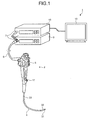
- FIG. 1 is a diagram schematically illustrating an overall configuration of an endoscope system according to an embodiment of the present invention.
- an endoscope apparatus 1 includes an endoscope 2, a universal cord 6, a connector 7, a light source device 9, a processor (control device) 10, and a display device 13.
- the endoscope 2 images an in-vivo image of a subject by inserting an insertion unit 4 into a body cavity of the subject and outputs an imaging signal.
- An electric cable bundle inside the universal cord 6 extends to a distal end of the insertion unit 4 of the endoscope 2 and is connected to an imaging apparatus provided at a distal end portion 31 of the insertion unit 4.
- the connector 7 is provided at a proximal end of the universal cord 6 and connected to the light source device 9 and the processor 10 to perform predetermined signal processing on an imaging signal output by the imaging apparatus at the distal end portion 31 connected to the universal cord 6, perform analog-digital conversion (A/D conversion) on the imaging signal, and output the signal as an image signal.
- A/D conversion analog-digital conversion
- the light source device 9 is formed of a white LED, for example. Pulsed white light illuminated by the light source device 9 passes through the connector 7 and the universal cord 6 to become illumination light radiated from the distal end of the insertion unit 4 of the endoscope 2 toward a subject.
- the processor 10 performs predetermined image processing on the image signal output from the connector 7 and controls the entire endoscope apparatus 1.
- the display device 13 displays the image signal processed by the processor 10.
- An operating unit 5 provided with various buttons and knobs to operate an endoscopic function is connected to a proximal end side of the insertion unit 4 of the endoscope 2.
- the operating unit 5 is provided with a treatment tool insertion port 17 from which a treatment tool such as forceps, an electric knife, or an examination probe is inserted into the body cavity of the subject.
- the insertion unit 4 is formed of the distal end portion 31 provided with the imaging apparatus, a bend portion 32 that is continuously connected to a proximal end side of the distal end portion 31 and freely bent in a plurality of directions, and a flexible tube 33 that is continuously connected to a proximal end side of the bend portion 32.
- the bend portion 32 is bent by an operation on a bend operation knob provided in the operating unit 5, and is freely bent in four directions including upward, downward, left and right directions according to traction and slackening of a bend wire inserted through the interior of the insertion unit 4.
- a light guide bundle (not shown) transmitting the illumination light from the light source device 9 is arranged in the endoscope 2, and an illumination lens (not shown) is arranged at an end to which the illumination light from the light guide bundle is emitted.
- the illumination lens is provided at the distal end portion 31 of the insertion unit 4 so that the illumination light is radiated toward the subject.
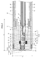
- FIG. 2 is a partial cross-sectional view of the distal end of the endoscope 2.
- FIG. 2 is a cross-sectional view obtained when the distal end is sectioned by a plane that is orthogonal to a substrate surface of an imaging unit provided at the distal end portion 31 of the endoscope 2 and is parallel to an optical axis direction of the imaging unit.
- FIG. 2 illustrates the distal end portion 31 and a part of the bend portion 32 of the insertion unit 4 of the endoscope 2.
- the bend portion 32 is freely bent in the four directions including the upward, downward, left and right directions according to traction and slackening of a bend wire 82 inserted through the interior of a bend tube 81 that is arranged on the inner side of a cover tube 42 to be described.
- An imaging apparatus 35 is provided inside the distal end portion 31 extending on the distal end side of the bend portion 32.
- the imaging apparatus 35 includes a lens unit 43 and an imaging unit 40 arranged on the proximal end side of the lens unit 43, and adheres to the inner side of a distal end body 41 by an adhesive 41a.
- the distal end body 41 is made of a rigid member that forms an inner space that accommodates the imaging apparatus 35.
- the outer periphery of the proximal end of the distal end body 41 is covered by the flexible cover tube 42.
- a member arranged on the proximal end side relative to the distal end body 41 is formed of a flexible member to allow the bend portion 32 to be bent.
- the distal end portion 31 where the distal end body 41 is arranged corresponds to a rigid portion of the insertion unit 4.
- a length La of the rigid portion corresponds to the length from the distal end of the insertion unit 4 to the proximal end of the distal end body 41.
- a length Lb corresponds to an outer diameter of the distal end of the insertion unit 4.
- the lens unit 43 includes a plurality of objective lenses 43a-1 to 43a-4 and a lens holder 43b holding the objective lenses 43a-1 to 43a-4, where a distal end of the lens holder 43b is fixed to the distal end body 41 by fitted and fixed to the interior of the distal end body 41.
- the imaging unit 40 includes a solid state image sensor 44 such as a CCD or CMOS which generates an electrical signal by performing photoelectric conversion on light received, an FPC board 45 (hereinafter referred to as an "FPC board 45") which extends in the optical axis direction from the solid state image sensor 44, a multi-layer substrate 46 which includes a plurality of conductor layers formed on a surface of the FPC board 45, and a glass lid 49 which adheres to the solid state image sensor 44 while covering a light-receiving surface of the solid state image sensor 44.
- electronic components 55 to 58 are mounted that constitute a drive circuit of the solid state image sensor 44.
- the multi-layer substrate 46 includes via holes 71 and 73 to establish electrical conduction among the plurality of conductor layers. Moreover, a distal end of each signal cable 48 of an electric cable bundle 47 is connected to a proximal end of the multi-layer substrate 46. An electronic component other than the electronic components constituting the drive circuit of the solid state image sensor 44 may be mounted on or in the multi-layer substrate 46 as well.
- each signal cable 48 extends in a proximal end direction of the insertion unit 4.
- the electric cable bundle 47 is inserted/arranged in the insertion unit 4 and extends up to the connector 7 through the operating unit 5 and the universal cord 6 illustrated in FIG. 1 .
- a subject image formed by the objective lenses 43a-1 to 43a-4 of the lens unit 43 is detected by the solid state image sensor 44 arranged at image-forming positions of the objective lenses 43a-1 to 43a-4 and converted into the imaging signal.
- the imaging signal is output to the processor 10 via the signal cable 48 connected to the FPC board 45 and the multi-layer substrate 46 as well as the connector 7.
- the solid state image sensor 44 adheres to the FPC board 45 and the multi-layer substrate 46.
- the solid state image sensor 44 and a connection portion between the solid state image sensor 44 and the FPC board 45 are covered by a metallic reinforcing member 52.
- the reinforcing member 52 is installed away from the solid state image sensor 44, the FPC board 45 and the multi-layer substrate 46.
- An outer periphery of a distal end portion of each of the imaging unit 40 and the electric cable bundle 47 is covered by a heat-shrinkable tube 50 in order to increase tolerance.
- An adhesive resin 51 fills a gap among components inside the heat-shrinkable tube 50.
- a solid state image sensor holder 53 holds the solid state image sensor 44 adhering to the glass lid 49 by fitting an outer peripheral surface of the glass lid 49 into an inner peripheral surface on the proximal end side of the solid state image sensor holder 53.
- An outer peripheral surface on the proximal end side of the solid state image sensor holder 53 is fitted to an inner peripheral surface on the distal end side of the reinforcing member 52.
- An outer peripheral surface on the proximal end side of the lens holder 43b is fitted to an inner peripheral surface on the distal end side of the solid state image sensor holder 53.
- the outer peripheral surface of the lens holder 43b, the outer peripheral surface of the solid state image sensor holder 53 and an outer peripheral surface on the distal end side of the heat-shrinkable tube 50 are fixed to an inner peripheral surface of the distal end of the distal end body 41 by the adhesive 41a.
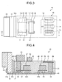
- FIG. 3 is a plan view of the imaging unit 40 as seen in planar view along a layered direction.
- FIG. 4 is a cross-sectional view taken along line A-A of FIG. 3 and obtained when the imaging unit 40 is sectioned by a plane perpendicular to the surface of the FPC board 45 and parallel to the optical axis direction of the solid state image sensor 44.
- the FPC board 45 extends toward the optical axis direction of the solid state image sensor 44 from a side opposite to the light-receiving surface of the solid state image sensor 44.
- the multi-layer substrate 46 formed by stacking a plurality of layers is formed on the surface of the FPC board 45 and is electrically and mechanically connected to the FPC board 45.
- a back side of the solid state image sensor 44 and a side face of the multi-layer substrate 46 on the side of the solid state image sensor adhere to each other by an adhesive 54b.
- the FPC board 45 will be described in detail later on.
- FIGS. 3 and 4 illustrate an example where, among the plurality of electronic components 55 to 58, the two electronic components 55 and 56 are mounted on the top surface of the multi-layer substrate 46. Also, among the plurality of electronic components 55 to 58, the two electronic components 57 and 58 are embedded inside the multi-layer substrate 46.
- connection lands 61 Formed on the multi-layer substrate 46 are two connection lands 61 to which the electronic component 55 is electrically connected, two connection lands 62 to which the electronic component 56 is connected, and a cable connection land 63 to which a conductor at the distal end of the signal cable 48 is electrically and mechanically connected.
- FIG. 3 illustrates an example where six cable connection lands 63 are provided to allow six signal cables 48 to be connected to the lands through solder or the like.
- a plurality of connection lands 64, 65A, 65B and 66 electrically connected to the FPC board 45 is formed on a bottom surface of the multi-layer substrate 46.
- a plurality of conductor layers is stacked inside the multi-layer substrate 46.
- Conductor layers 67, 68 and 69 are illustrated in the cross section in FIG. 4 .
- a plurality of via holes 71 to 76 is formed inside the multi-layer substrate 46.
- Each of the plurality of conductor layers including the conductor layers 67 to 69 is formed to be electrically connected to any of the plurality of via holes 71 to 76.
- the electronic components 57 and 58 embedded inside the multi-layer substrate 46 are mounted on the conductor layers 67 and 68, respectively, which are second layers from the outermost layer being the bottom surface of the multi-layer substrate 46.
- the electronic component is mounted or embedded on or in the conductor layer formed in the outermost layer (such as a layer at the same level as the connection lands 64, 65A, 65B and 66 or a layer at the same level as the connection lands 61 and 62)
- the electronic components 57 and 58 are possibly disconnected by heat generated in mounting the electronic components 55 and 56 and connecting the signal cable 48 to the surface of the multi-layer substrate 46 or connecting the FPC board 45 and the multi-layer substrate 46, whereby the conductor layers 67 and 68 to which the electronic components 57 and 58 are connected are preferably formed on the second layer or inward from the outermost layer.
- the thickness of the multi-layer substrate 46 is increased when the conductor layers are formed on a third layer or inward so that, in order to achieve connection reliability and reduce the thickness of the multi-layer substrate 46, the conductor layers are more preferably formed on the second layer from the outermost layer.
- FIG. 5 is an enlarged view of the connection portion between the solid state image sensor 44 and the FPC board 45 of the imaging unit 40 illustrated in FIG. 4 .
- the FPC board 45 includes an insulating base material 45a, a first surface-side wiring layer 45b formed on the side of a first surface of the base material 45a nearer the solid state image sensor 44, a first surface-side electrical insulating film 45c insulating the first surface-side wiring layer 45b, a second surface-side wiring layer 45d formed on the side of a second surface of the base material 45a being a back side of the first surface nearer the solid state image sensor 44, and a second surface-side electrical insulating film 45e insulating the second surface-side wiring layer 45d.
- the FPC board 45 further includes an inner lead 45f that is connected to an electrode pad (not shown) formed in the solid state image sensor 44 and is formed from the first surface-side wiring layer 45b. It is preferable that a wiring pattern on the first surface side, a connection land to be connected to the multi-layer substrate 46 and an alignment recognition mark used in connecting the multi-layer substrate 46 are formed on the first surface-side wiring layer 45b.
- the recognition mark provided in the first surface-side wiring layer 45b to perform alignment at the time of connecting the multi-layer substrate, the position of the multi-layer substrate relative to the connection portion of the solid state image sensor 44 and the inner lead 45f varies less.
- the first surface-side electrical insulating film 45c is made open at a position corresponding to the recognition mark, whereby the accuracy of recognition can be increased.
- the inner lead 45f is bent about 90° along the side of the light-receiving surface of the rectangular parallelepiped solid state image sensor 44 from the side face thereof, and is electrically connected to an electrode pad 44a formed on the side of the light-receiving surface of the solid state image sensor 44 through a bump 44b or the like.
- the periphery of a connection portion between the inner lead 45f and the electrode pad 44a is covered by an insulating sealing resin 54a.
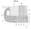
- FIG. 6 illustrates a cross-sectional view of a conventional FPC board.
- a conventional FPC board 45' is adapted such that an inner lead 45f is formed from a second surface-side wiring layer 45d, and a base material 45a is located in a direction in which the inner lead 45f is bent.
- the FPC board 45 and the FPC board 45' having a layered structure there is a variation in layer thicknesses d1, d2, d3, d4, and d5.
- the length of the inner lead 45f is determined in consideration of a distance from the inner lead 45f to the side face of the solid state image sensor 44, a position at which each of the FPC boards 45, 45' and the solid state image sensor 44 are connected, and a position (height) of the electrode pad 44a of the solid state image sensor 44, where the inner lead 45f becomes shorter or longer than a predetermined length when the distance from the inner lead 45f to the side face of the solid state image sensor 44 varies considerably so that connection to the electrode pad 44a becomes less reliable in some cases.
- the variation in the distance from the inner lead 45f to the side face of the solid state image sensor 44 is caused by only the thickness d1 of the first surface-side electrical insulating film 45c in the first embodiment
- the variation increases in a conventional example as the variation is caused by the thicknesses d1 + d2 + d3 of the base material 45a, the first surface-side wiring layer 45b and the first surface-side electrical insulating film 45c added together so that the connection possibly becomes less reliable.
- the variation in the distance from the inner lead 45f to the side face of the solid state image sensor 44 can be decreased to thus be able to maintain the connection reliability.
- the inner lead 45f is bent about 90° along the side of the light-receiving surface of the solid state image sensor 44 from the side face thereof and connected to the electrode pad 44a, so that the inner lead does not easily bulge out when bent to thus be able to prevent an increase in size of the imaging unit 40.
- the multi-layer substrate 46 is connected to a connection land of the first surface-side wiring layer 45b from which the inner lead 45f extends, so that a relative position between the connection portion of the inner lead 45f and the electrode pad 44a and the multi-layer substrate 46 varies less and, as a result, the imaging unit 40 can have a decreased width and a shorter rigid portion to thus be reduced in size.
- the position gap between the first surface-side wiring layer 45b and the second surface-side wiring layer 45d causes the increase in variation of the relative position between the connection portion of the inner lead 45f and the electrode pad 44a and the multi-layer substrate 46.
- FIG. 7 is an enlarged cross-sectional view illustrating a connection portion between a connection land 65A of the multi-layer substrate 46 and a connection land 45g of the FPC board 45.
- the connection land 65A of the multi-layer substrate 46 and the connection land 45g of the FPC board 45 are electrically connected by a bump 45h-1 such as an Au stud bump or a solder bump.
- connection portion of the connection land 65A of the multi-layer substrate 46 is covered by an insulating film 46a such as a solder resist, whereas the surface excluding the connection portion of the connection land 45g of the FPC board 45 is covered by a first surface-side electrical insulating film 45c such as a solder resist.
- the sum of a thickness r1 of the first surface-side electrical insulating film 45c and a thickness r2 of the insulating film 46a is preferably smaller than the sum of a thickness r3 of the connection land 45g, a height r4 of the bump 45h-1 and a thickness r5 of the connection land 65A.
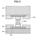
- the bump used in connection may be employed in a way that two bumps 45h-2 that are small in height are placed on top of each other, or the bump 45h-2 small in height is disposed on each of the connection land 45g and the connection land 65A.
- the sum of the thickness of the first surface-side electrical insulating film 45c and the thickness of the insulating film 46a is preferably smaller than the sum of the thickness of the connection land 45g, the total height of the bump 45h-2 and the thickness of the connection land 65A.
- a connector terminal 37 used for examination is formed on an FPC board 45A (refer to FIG. 10 ) before cut-out in order to inspect an electrical property at the time of connecting the FPC board 45 and the solid state image sensor 44 and connecting the FPC board 45 and the multi-layer substrate 46.
- the number of the connector terminals 37 corresponds to the number of the inner leads 45f, and the electrical property is inspected by bringing a terminal of an examination device into contact with the connector terminal 37.
- the connector terminal 37 can also be formed outside a product area indicated with a dotted line in FIG. 10 to extract an output signal of the electronic component mounted on or in the multi-layer substrate 46.
- the connector terminal 37 is used to be able to inspect connection quality in each process after connecting the inner lead 45f of the FPC board 45 and the electrode pad of the solid state image sensor 44 (INNER LEAD BONDING: ILB), whereby a defective product can be detected early to thus be able to decrease a manufacturing cost.
- the FPC board 45A before cutting out a use area is connected to the multi-layer substrate 46 and the solid state image sensor 44 and thereafter cut in a connection area indicated with the dotted line in FIG. 10 .
- the FPC board 45A is conventionally cut at a predetermined cut position on the FPC board 45A where, when there is a large gap in the connection position between the FPC board 45A and the multi-layer substrate 46, the FPC board sometimes cannot be cut at the predetermined cut position or, when cut at the predetermined cut position, the outer shape of the imaging unit 40 is sometimes increased in size.
- the FPC board 45A is preferably cut with reference to the outer shape of the multi-layer substrate 46.
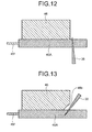
- the FPC board 45A may be cut by placing a cutting tool 38 along the multi-layer substrate 46 from the side of the multi-layer substrate 46 (refer to FIG. 11 ), placing the cutting tool 38 along the outer shape of the multi-layer substrate 46 seen through the FPC board from the side of the FPC board 45A (refer to FIG. 12 ), or forming a chamfered portion 46b at a bottom face of the multi-layer substrate 46, placing the cutting tool 38 along the chamfered portion 46b and cutting the FPC board 45A at a position inside the outer shape of the multi-layer substrate 46 (refer to FIG. 13 ).
- an effect similar to that of the first embodiment can also be obtained when one or more electronic components are directly mounted on the FPC board 45 or when a cavity-formed rigid substrate 60 having a recess (cavity) in which an electronic component is mounted is connected to the FPC board.
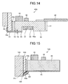
- FIG. 14 is a side view of an imaging unit according to a modification of the first embodiment.
- the cavity-formed rigid substrate 60 is connected to an FPC board 45.
- Electronic components 57 and 58 are mounted in a cavity 60a of the cavity-formed rigid substrate 60.
- the cavity 60a is preferably formed not at a rear end (end at which a signal cable 48 is connected) but at a center of the cavity-formed rigid substrate 60 in order to improve workability in connecting the signal cable 48 to a top surface of the cavity-formed rigid substrate 60.
- a height h1 of the rear end of the cavity-formed rigid substrate 60 is preferably roughly equal to the sum of a height h2 of a front end of the substrate and a thickness h3 of the FPC board 45 but, when the thickness h3 of the FPC board 45 is small, the height h1 of the rear end of the cavity-formed rigid substrate 60 may be formed to equal the height h2 of the front end.
- Such configuration allows the imaging unit 40 to be received and fixed on a flat surface at the time of soldering the cable 48, thereby facilitating the soldering work. The similar effect can be achieved when a bottom surface side of the imaging unit 40 is flat as with the first embodiment.
- An imaging unit according to a second embodiment is different from the first embodiment in that a solid state image sensor includes an oblique electrode, to which an inner lead of an FPC board is connected.
- FIG. 15 is a side view of the imaging unit according to the second embodiment.
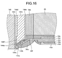
- FIG. 16 is an enlarged cross-sectional view of a connection portion between the solid state image sensor and the FPC board of the imaging unit illustrated in FIG. 15 .
- a solid state image sensor 144 includes a notch 145 from which an electrode pad 144a is exposed to the side of an FPC board 45.
- the notch 145 is formed to traverse the surface of the solid state image sensor 144 on the side of the FPC board 45 so that a plurality of electrode pads 144a is exposed to the side of the FPC board 45.
- the notch 145 is a slope formed at a predetermined angle with a light-receiving unit 144d by chemical or physical etching or mechanical cutting.
- the solid state image sensor 144 and a glass lid 149 adhere to each other by a bonding layer 54d made of a transparent adhesive or the like. Moreover, a protective film 144e is formed on a surface of a back side of the light-receiving unit 144d of a body 144c.
- An oblique electrode 144f connected to the electrode pad 144a is formed on the slope of the notch 145, and an inner lead 45f of the FPC board 45 is electrically connected to the oblique electrode 144f through a bump 144b.
- a connection portion between the inner lead 45f and the oblique electrode 144f is sealed by a sealing resin 54a.
- the notch 145 is formed so as to house the sealing resin 54a in the notch 145, thereby preventing an increase in size of the imaging unit due to the sealing resin 54a sticking out.
- an adhesive 54c reinforcing an interface between the FPC board 45 and a multi-layer substrate 46 seeps toward the inner lead, the base of which is then reinforced to be able to prevent deformation of the inner lead.
- the FPC board 45 When the inner lead 45f extending from the FPC board 45 is directly connected in parallel with the oblique electrode 144f, the FPC board 45 needs to be extended in length in order to prevent interference between a corner C2 of the multi-layer substrate 46 and a corner C1 of the solid state image sensor 144 as illustrated in FIG. 17 .
- the multi-layer substrate 46 and electronic components 55 and 56 lie outside a projected area on the surface orthogonal to an optical axis direction of the solid state image sensor 144, thereby hindering a diameter reduction of the imaging unit 140.
- the inner lead 45f can be bent to fit the multi-layer substrate 46 and the electronic components 55 and 56 within the projected area projected in the optical axis direction of the solid state image sensor 144 but, as illustrated in FIG. 17 , the length of a rigid portion of the imaging unit 140 (from the glass lid 149 to a rear end of the multi-layer substrate 46) is increased when the inner lead 45f is bent after connecting the FPC board 45 and the solid state image sensor 144.
- the length of the rigid portion of the imaging unit 140 can be decreased while preventing interference between the solid state image sensor 144 and the multi-layer substrate 46 by bending the inner lead 45f at a predetermined angle and then connecting it to the oblique electrode 144f.
- the bend angle of the inner lead 45f is adjusted to an angle such that the FPC board 45 is parallel to the optical axis direction of the solid state image sensor 144 after connecting the inner lead 45f and the oblique electrode 144f.
- FIG. 18 is a cross-sectional view illustrating the connection of the inner lead 45f to the oblique electrode 144f.
- the inner lead 45f is connected to the oblique electrode 144f while fixing the FPC board 45 by a tool and applying pressure to the connection portion by a bonding tool 146 where, when the bend angle ⁇ 1 is set smaller than or equal to the bend angle ⁇ 2 after connection (the inner lead indicated with a dotted line in FIG. 18 ), there is a possibility of a break in the lead because tensile stress applied to a lead bend C3 at the time of connection is larger than when the bend angle ⁇ 1 is set larger than the bend angle ⁇ 2 after connection (the inner lead indicated with a solid line in FIG. 18 ).
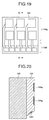
- an examination pad for the solid state image sensor 144 is formed at a back side of the light-receiving unit 144d of the solid state image sensor 144.
- FIG. 19 is a diagram illustrating the examination pad formed at the back side of a light-receiving surface of the solid state image sensor 144
- FIG. 20 is a cross-sectional view taken along line B-B of FIG. 19 illustrating the solid state image sensor 144.
- An examination pad 144g is formed at the back side of the solid state image sensor 144.
- a probe mark generated at the time of the examination is sometimes left on the oblique electrode.
- Flatness of the surface is deteriorated due to the probe mark when the bump 144b is formed on the oblique electrode on which the probe mark is left, whereby the bonding may possibly become less reliable.
- the examination pad 144g is preferably formed separately from the oblique electrode 144f. Note that a bonding pad different from the oblique electrode may be provided at the back side of the solid state image sensor 144 as well.
- a connection land to which the multi-layer substrate is mounted is formed in a first surface-side wiring layer in which the inner lead is formed, so that a position gap between the connection portion of the inner lead and the connection position of the multi-layer substrate can be decreased to thus be able to prevent the increase in length of the rigid portion.
- a base material of the FPC board is arranged at the back side of the inner lead to allow the height above the inner lead of the imaging unit to be decreased by the thickness of the base material, whereby a larger (taller) electronic component can be mounted within the projected area projected in the optical axis direction of the solid state image sensor. That is, the increase in size of the imaging unit can be prevented even when a tall electronic component is mounted.
- FIG. 21 is a cross-sectional view of a part of an imaging unit according to a modification of the second embodiment.
- a groove-like opening 147 is formed in a solid state image sensor 144 to expose an electrode pad 144a on the side of an FPC board 45, and an oblique electrode 144f is formed in the opening 147 to electrically connect with the electrode pad 144a. Similar to the notch 145, the opening 147 is formed to traverse the surface of the solid state image sensor 144 on the side of the FPC board 45 such that a plurality of electrode pads 144a is all exposed on the side of the FPC board 45.
- an adhesive 54b for sealing the connection between an inner lead 45f and the oblique electrode 144f is contained in the opening 147 with no possibility of leaking outside the solid state image sensor 144, whereby an increase in size of the imaging unit can be prevented.
Landscapes
- Health & Medical Sciences (AREA)
- Life Sciences & Earth Sciences (AREA)
- Surgery (AREA)
- Engineering & Computer Science (AREA)
- Biomedical Technology (AREA)
- Molecular Biology (AREA)
- Pathology (AREA)
- Radiology & Medical Imaging (AREA)
- Nuclear Medicine, Radiotherapy & Molecular Imaging (AREA)
- Biophysics (AREA)
- Physics & Mathematics (AREA)
- Heart & Thoracic Surgery (AREA)
- Medical Informatics (AREA)
- Optics & Photonics (AREA)
- Animal Behavior & Ethology (AREA)
- General Health & Medical Sciences (AREA)
- Public Health (AREA)
- Veterinary Medicine (AREA)
- Multimedia (AREA)
- Signal Processing (AREA)
- Endoscopes (AREA)
- Studio Devices (AREA)
- Instruments For Viewing The Inside Of Hollow Bodies (AREA)
Abstract
Description
- The present invention relates to an imaging unit and an endoscope apparatus, the imaging unit being provided at a distal end of an insertion unit of an endoscope that is configured to be inserted into a subject to image the inside of the subject.
- Endoscope apparatuses have been widely used to perform various examinations in a medical field and an industrial field. Among those apparatuses, a medical endoscope apparatus is widely used because an in-vivo image of a body cavity can be acquired without making an incision on a subject such as a patient by inserting an elongated, flexible insertion unit provided with an image sensor at a distal end thereof into the body cavity of the subject and, at the same time, a curative treatment can be performed as needed by projecting a treatment tool from the distal end of the insertion unit.
- Fitted to the distal end of the insertion unit of such endoscope apparatus is an imaging unit including a solid state image sensor and a flexible printed circuit board (hereinafter referred to as an FPC board) employing Tape Automated Bonding (TAB) or the like and populated with electronic components such as a capacitor and an IC chip constituting a drive circuit of the solid state image sensor, where a signal cable is soldered to the FPC board of the imaging unit. An inner lead exposed from an end face of the FPC board is bent along a side of a light-receiving surface of the solid state image sensor from a side face thereof, and is connected to an electrode pad formed in the solid state image sensor.
- As a technique of connecting the inner lead and the electrode pad, there is disclosed a technique in which an insulating carrier tape material of an FPC board is arranged on the side of a solid state image sensor, the FPC board being formed of the carrier tape material and a wiring layer including an inner lead formed from metal foil such as copper foil adhering to the carrier tape material (refer to
Patent Literature 1, for example).Patent Literature 1 also discloses a technique in which the inner lead extending from a wiring pattern on the back side of a base material (back side of a surface on which an electronic component is mounted) of the FPC board is connected to the electrode pad of the solid state image sensor, the FPC board including the wiring pattern formed on both sides of the base material. - Patent Literature 1:
Japanese Patent Application Publication No. 2001-257937 - However, when the inner lead is bent about 90° along the side of the light-receiving surface of the solid state image sensor from the side face thereof and connected thereto, the base material is formed on the inner side (in a bent direction) of the inner lead in the technique disclosed in
Patent Literature 1, thereby causing a problem that a bent portion of the inner lead is bulged out by the amount corresponding to the thickness of the base material to cause the imaging unit to increase in size. Moreover, when the electronic component is mounted in a layer different from the wiring layer in which the inner lead is formed, a position gap between the wiring layers causes an increased gap in a relative position between an inner lead connection portion and a mounted component in some cases where the imaging unit exceeds an allowable dimension. - The present invention has been made in view of the foregoing, and an object of the invention is to provide an imaging unit and an endoscope apparatus that prevent an increase in size of the unit and thereby decrease a diameter of a distal end of an insertion unit.
- In order to solve the above described problems and achieve the object, an imaging unit according to the invention includes: a solid state image sensor configured to receive light and to perform photoelectric conversion on the received light to generate an electrical signal; a flexible printed circuit board having an inner lead connected to an electrode pad of the solid state image sensor and extending from the solid state image sensor in a direction opposite to where a light-receiving surface of the solid state image sensor is provided; and one or more electronic components mounted on a first surface of the flexible printed circuit board, the first surface being on a side where the solid state image sensor is provided. The flexible printed circuit board includes an insulating base material, a first surface-side wiring layer on the base material on a side of the first surface, and a first surface-side electrical insulating film for insulating the first surface-side wiring layer, and the inner lead extends from the first surface-side wiring layer.
- In the imaging unit according to the above-described invention, the flexible printed circuit board further includes a second surface-side wiring layer on the base material on a side of a second surface opposite to the first surface, and a second surface-side electrical insulating film for insulating the second surface-side wiring layer.
- In the imaging unit according to the above-described invention, the inner lead is bent from a side of the solid state image sensor having a rectangular parallelepiped shape along the light-receiving surface.
- In the imaging unit according to the above-described invention, the solid state image sensor includes a notch or an opening for exposing the electrode pad on a side of the flexible printed circuit board, and an oblique electrode to be connected to the electrode pad through the notch or the opening, and the inner lead is connected to the oblique electrode.
- In the imaging unit according to the above-described invention, the inner lead is bent in such a way that the flexible printed circuit board is parallel to an optical axis direction of the solid state image sensor.
- In the imaging unit according to the above-described invention, the flexible printed circuit board and the one or more electronic components are housed within a projected area on a surface orthogonal to an optical axis direction of the solid state image sensor.
- In the imaging unit according to the above-described invention, a recognition mark used for mounting the one or more electronic components is formed on the first surface-side wiring layer.
- An endoscope apparatus includes an insertion unit, at a distal end of which the imaging unit according to the above-described invention is provided.
- According to the present invention, the inner lead is connected to the electrode pad by arranging the base material of the flexible printed circuit board on the outer side, whereby the imaging unit and the endoscope apparatus can be smaller in size.
-
-
FIG. 1 is a diagram schematically illustrating an overall configuration of an endoscope system according to an embodiment of the present invention. -
FIG. 2 is a partial cross-sectional view of a distal end of an endoscope illustrated inFIG. 1 . -
FIG. 3 is a plan view of an imaging unit illustrated inFIG. 2 as seen in planar view along a layered direction. -
FIG. 4 is a cross-sectional view taken along line A-A ofFIG. 3 . -
FIG. 5 is an enlarged view of a part of the imaging unit illustrated inFIG. 4 . -
FIG. 6 is a cross-sectional view illustrating an example of a conventional flexible printed circuit board. -
FIG. 7 is a cross-sectional view illustrating a connection portion between an FPC board and a multi-layer substrate. -
FIG. 8 is a cross-sectional view illustrating a connection portion between the FPC board and the multi-layer substrate. -
FIG. 9 is a cross-sectional view illustrating a connection portion between the FPC board and the multi-layer substrate. -
FIG. 10 is a diagram illustrating the FPC board before a use area is cut out. -
FIG. 11 is a diagram illustrating cutting of the FPC board illustrated inFIG. 10 . -
FIG. 12 is a diagram illustrating cutting of the FPC board illustrated inFIG. 10 . -
FIG. 13 is a diagram illustrating cutting of the FPC board illustrated inFIG. 10 . -
FIG. 14 is a side view of an imaging unit according to a modification of a first embodiment. -
FIG. 15 is a side view of an imaging unit according to a second embodiment. -
FIG. 16 is an enlarged cross-sectional view of a connection portion between a solid state image sensor and an FPC board of the imaging unit illustrated inFIG. 15 . -
FIG. 17 is a diagram illustrating an undesirable example of a method of manufacturing the imaging unit according to the second embodiment. -
FIG. 18 is a cross-sectional view illustrating connection of an inner lead to an oblique electrode. -
FIG. 19 is a diagram illustrating an examination pad and a bonding pad formed on a back side of a light-receiving surface of the solid state image sensor. -
FIG. 20 is a cross-sectional view taken along line B-B ofFIG. 19 illustrating the solid state image sensor. -
FIG. 21 is a cross-sectional view of a part of an imaging unit according to a modification of the second embodiment. - As modes for carrying out the invention (hereinafter referred to as "embodiment(s)"), an endoscope apparatus having an imaging module will be described below. The present invention is not to be limited by the embodiments. The same reference signs are used to designate the same elements throughout the drawings. The drawings being provided schematically, one needs to further keep in mind that the relationship between the thickness and width of each member as well as a ratio of each member are different from actual ones. Moreover, the dimension and ratio of some parts are different among the drawings.
-
FIG. 1 is a diagram schematically illustrating an overall configuration of an endoscope system according to an embodiment of the present invention. As illustrated inFIG. 1 , anendoscope apparatus 1 includes anendoscope 2, auniversal cord 6, a connector 7, alight source device 9, a processor (control device) 10, and adisplay device 13. - The
endoscope 2 images an in-vivo image of a subject by inserting aninsertion unit 4 into a body cavity of the subject and outputs an imaging signal. An electric cable bundle inside theuniversal cord 6 extends to a distal end of theinsertion unit 4 of theendoscope 2 and is connected to an imaging apparatus provided at adistal end portion 31 of theinsertion unit 4. - The connector 7 is provided at a proximal end of the
universal cord 6 and connected to thelight source device 9 and theprocessor 10 to perform predetermined signal processing on an imaging signal output by the imaging apparatus at thedistal end portion 31 connected to theuniversal cord 6, perform analog-digital conversion (A/D conversion) on the imaging signal, and output the signal as an image signal. - The
light source device 9 is formed of a white LED, for example. Pulsed white light illuminated by thelight source device 9 passes through the connector 7 and theuniversal cord 6 to become illumination light radiated from the distal end of theinsertion unit 4 of theendoscope 2 toward a subject. - The
processor 10 performs predetermined image processing on the image signal output from the connector 7 and controls theentire endoscope apparatus 1. Thedisplay device 13 displays the image signal processed by theprocessor 10. - An
operating unit 5 provided with various buttons and knobs to operate an endoscopic function is connected to a proximal end side of theinsertion unit 4 of theendoscope 2. Theoperating unit 5 is provided with a treatmenttool insertion port 17 from which a treatment tool such as forceps, an electric knife, or an examination probe is inserted into the body cavity of the subject. - The
insertion unit 4 is formed of thedistal end portion 31 provided with the imaging apparatus, abend portion 32 that is continuously connected to a proximal end side of thedistal end portion 31 and freely bent in a plurality of directions, and aflexible tube 33 that is continuously connected to a proximal end side of thebend portion 32. Thebend portion 32 is bent by an operation on a bend operation knob provided in theoperating unit 5, and is freely bent in four directions including upward, downward, left and right directions according to traction and slackening of a bend wire inserted through the interior of theinsertion unit 4. - A light guide bundle (not shown) transmitting the illumination light from the
light source device 9 is arranged in theendoscope 2, and an illumination lens (not shown) is arranged at an end to which the illumination light from the light guide bundle is emitted. The illumination lens is provided at thedistal end portion 31 of theinsertion unit 4 so that the illumination light is radiated toward the subject. - Next, the configuration of the
distal end portion 31 of theendoscope 2 will be described in detail.FIG. 2 is a partial cross-sectional view of the distal end of theendoscope 2.FIG. 2 is a cross-sectional view obtained when the distal end is sectioned by a plane that is orthogonal to a substrate surface of an imaging unit provided at thedistal end portion 31 of theendoscope 2 and is parallel to an optical axis direction of the imaging unit.FIG. 2 illustrates thedistal end portion 31 and a part of thebend portion 32 of theinsertion unit 4 of theendoscope 2. - As illustrated in
FIG. 2 , thebend portion 32 is freely bent in the four directions including the upward, downward, left and right directions according to traction and slackening of abend wire 82 inserted through the interior of abend tube 81 that is arranged on the inner side of acover tube 42 to be described. Animaging apparatus 35 is provided inside thedistal end portion 31 extending on the distal end side of thebend portion 32. - The
imaging apparatus 35 includes alens unit 43 and animaging unit 40 arranged on the proximal end side of thelens unit 43, and adheres to the inner side of adistal end body 41 by an adhesive 41a. Thedistal end body 41 is made of a rigid member that forms an inner space that accommodates theimaging apparatus 35. The outer periphery of the proximal end of thedistal end body 41 is covered by theflexible cover tube 42. A member arranged on the proximal end side relative to thedistal end body 41 is formed of a flexible member to allow thebend portion 32 to be bent. Thedistal end portion 31 where thedistal end body 41 is arranged corresponds to a rigid portion of theinsertion unit 4. A length La of the rigid portion corresponds to the length from the distal end of theinsertion unit 4 to the proximal end of thedistal end body 41. Note that a length Lb corresponds to an outer diameter of the distal end of theinsertion unit 4. - The
lens unit 43 includes a plurality ofobjective lenses 43a-1 to 43a-4 and alens holder 43b holding theobjective lenses 43a-1 to 43a-4, where a distal end of thelens holder 43b is fixed to thedistal end body 41 by fitted and fixed to the interior of thedistal end body 41. - The
imaging unit 40 includes a solidstate image sensor 44 such as a CCD or CMOS which generates an electrical signal by performing photoelectric conversion on light received, an FPC board 45 (hereinafter referred to as an "FPC board 45") which extends in the optical axis direction from the solidstate image sensor 44, amulti-layer substrate 46 which includes a plurality of conductor layers formed on a surface of theFPC board 45, and aglass lid 49 which adheres to the solidstate image sensor 44 while covering a light-receiving surface of the solidstate image sensor 44. On or in themulti-layer substrate 46 of theimaging unit 40,electronic components 55 to 58 are mounted that constitute a drive circuit of the solidstate image sensor 44. Themulti-layer substrate 46 includes viaholes signal cable 48 of anelectric cable bundle 47 is connected to a proximal end of themulti-layer substrate 46. An electronic component other than the electronic components constituting the drive circuit of the solidstate image sensor 44 may be mounted on or in themulti-layer substrate 46 as well. - A proximal end of each
signal cable 48 extends in a proximal end direction of theinsertion unit 4. Theelectric cable bundle 47 is inserted/arranged in theinsertion unit 4 and extends up to the connector 7 through theoperating unit 5 and theuniversal cord 6 illustrated inFIG. 1 . - A subject image formed by the
objective lenses 43a-1 to 43a-4 of thelens unit 43 is detected by the solidstate image sensor 44 arranged at image-forming positions of theobjective lenses 43a-1 to 43a-4 and converted into the imaging signal. The imaging signal is output to theprocessor 10 via thesignal cable 48 connected to theFPC board 45 and themulti-layer substrate 46 as well as the connector 7. - The solid
state image sensor 44 adheres to theFPC board 45 and themulti-layer substrate 46. The solidstate image sensor 44 and a connection portion between the solidstate image sensor 44 and theFPC board 45 are covered by a metallic reinforcingmember 52. In order to prevent the influence of external static electricity against theelectronic components 55 to 58 on theFPC board 45, the reinforcingmember 52 is installed away from the solidstate image sensor 44, theFPC board 45 and themulti-layer substrate 46. - An outer periphery of a distal end portion of each of the
imaging unit 40 and theelectric cable bundle 47 is covered by a heat-shrinkable tube 50 in order to increase tolerance. Anadhesive resin 51 fills a gap among components inside the heat-shrinkable tube 50. - A solid state
image sensor holder 53 holds the solidstate image sensor 44 adhering to theglass lid 49 by fitting an outer peripheral surface of theglass lid 49 into an inner peripheral surface on the proximal end side of the solid stateimage sensor holder 53. An outer peripheral surface on the proximal end side of the solid stateimage sensor holder 53 is fitted to an inner peripheral surface on the distal end side of the reinforcingmember 52. An outer peripheral surface on the proximal end side of thelens holder 43b is fitted to an inner peripheral surface on the distal end side of the solid stateimage sensor holder 53. While each member is fitted in this manner, the outer peripheral surface of thelens holder 43b, the outer peripheral surface of the solid stateimage sensor holder 53 and an outer peripheral surface on the distal end side of the heat-shrinkable tube 50 are fixed to an inner peripheral surface of the distal end of thedistal end body 41 by the adhesive 41a. - The
imaging unit 40 will now be described.FIG. 3 is a plan view of theimaging unit 40 as seen in planar view along a layered direction.FIG. 4 is a cross-sectional view taken along line A-A ofFIG. 3 and obtained when theimaging unit 40 is sectioned by a plane perpendicular to the surface of theFPC board 45 and parallel to the optical axis direction of the solidstate image sensor 44. - The
FPC board 45 extends toward the optical axis direction of the solidstate image sensor 44 from a side opposite to the light-receiving surface of the solidstate image sensor 44. Themulti-layer substrate 46 formed by stacking a plurality of layers is formed on the surface of theFPC board 45 and is electrically and mechanically connected to theFPC board 45. A back side of the solidstate image sensor 44 and a side face of themulti-layer substrate 46 on the side of the solid state image sensor adhere to each other by an adhesive 54b. TheFPC board 45 will be described in detail later on. - Among the plurality of
electronic components 55 to 58 constituting the drive circuit of the solidstate image sensor 44, one or more electronic components are mounted on a top surface of themulti-layer substrate 46 while one or more other electronic components are embedded inside themulti-layer substrate 46.FIGS. 3 and 4 illustrate an example where, among the plurality ofelectronic components 55 to 58, the twoelectronic components multi-layer substrate 46. Also, among the plurality ofelectronic components 55 to 58, the twoelectronic components multi-layer substrate 46. - Formed on the
multi-layer substrate 46 are two connection lands 61 to which theelectronic component 55 is electrically connected, two connection lands 62 to which theelectronic component 56 is connected, and acable connection land 63 to which a conductor at the distal end of thesignal cable 48 is electrically and mechanically connected.FIG. 3 illustrates an example where six cable connection lands 63 are provided to allow sixsignal cables 48 to be connected to the lands through solder or the like. A plurality of connection lands 64, 65A, 65B and 66 electrically connected to theFPC board 45 is formed on a bottom surface of themulti-layer substrate 46. - A plurality of conductor layers is stacked inside the
multi-layer substrate 46. Conductor layers 67, 68 and 69 are illustrated in the cross section inFIG. 4 . Moreover, a plurality of viaholes 71 to 76 is formed inside themulti-layer substrate 46. Each of the plurality of conductor layers including the conductor layers 67 to 69 is formed to be electrically connected to any of the plurality of viaholes 71 to 76. - As illustrated in
FIG. 4 , theelectronic components multi-layer substrate 46 are mounted on the conductor layers 67 and 68, respectively, which are second layers from the outermost layer being the bottom surface of themulti-layer substrate 46. When the electronic component is mounted or embedded on or in the conductor layer formed in the outermost layer (such as a layer at the same level as the connection lands 64, 65A, 65B and 66 or a layer at the same level as the connection lands 61 and 62), theelectronic components electronic components signal cable 48 to the surface of themulti-layer substrate 46 or connecting theFPC board 45 and themulti-layer substrate 46, whereby the conductor layers 67 and 68 to which theelectronic components multi-layer substrate 46 is increased when the conductor layers are formed on a third layer or inward so that, in order to achieve connection reliability and reduce the thickness of themulti-layer substrate 46, the conductor layers are more preferably formed on the second layer from the outermost layer. -
FIG. 5 is an enlarged view of the connection portion between the solidstate image sensor 44 and theFPC board 45 of theimaging unit 40 illustrated inFIG. 4 . TheFPC board 45 includes an insulatingbase material 45a, a first surface-side wiring layer 45b formed on the side of a first surface of thebase material 45a nearer the solidstate image sensor 44, a first surface-side electrical insulatingfilm 45c insulating the first surface-side wiring layer 45b, a second surface-side wiring layer 45d formed on the side of a second surface of thebase material 45a being a back side of the first surface nearer the solidstate image sensor 44, and a second surface-side electrical insulatingfilm 45e insulating the second surface-side wiring layer 45d. TheFPC board 45 further includes aninner lead 45f that is connected to an electrode pad (not shown) formed in the solidstate image sensor 44 and is formed from the first surface-side wiring layer 45b. It is preferable that a wiring pattern on the first surface side, a connection land to be connected to themulti-layer substrate 46 and an alignment recognition mark used in connecting themulti-layer substrate 46 are formed on the first surface-side wiring layer 45b. By using the recognition mark provided in the first surface-side wiring layer 45b to perform alignment at the time of connecting the multi-layer substrate, the position of the multi-layer substrate relative to the connection portion of the solidstate image sensor 44 and theinner lead 45f varies less. Moreover, the first surface-side electrical insulatingfilm 45c is made open at a position corresponding to the recognition mark, whereby the accuracy of recognition can be increased. - The
inner lead 45f is bent about 90° along the side of the light-receiving surface of the rectangular parallelepiped solidstate image sensor 44 from the side face thereof, and is electrically connected to anelectrode pad 44a formed on the side of the light-receiving surface of the solidstate image sensor 44 through abump 44b or the like. The periphery of a connection portion between theinner lead 45f and theelectrode pad 44a is covered by an insulatingsealing resin 54a. -
FIG. 6 illustrates a cross-sectional view of a conventional FPC board. A conventional FPC board 45' is adapted such that aninner lead 45f is formed from a second surface-side wiring layer 45d, and abase material 45a is located in a direction in which theinner lead 45f is bent. In theFPC board 45 and the FPC board 45' having a layered structure, there is a variation in layer thicknesses d1, d2, d3, d4, and d5. The length of theinner lead 45f is determined in consideration of a distance from theinner lead 45f to the side face of the solidstate image sensor 44, a position at which each of theFPC boards 45, 45' and the solidstate image sensor 44 are connected, and a position (height) of theelectrode pad 44a of the solidstate image sensor 44, where theinner lead 45f becomes shorter or longer than a predetermined length when the distance from theinner lead 45f to the side face of the solidstate image sensor 44 varies considerably so that connection to theelectrode pad 44a becomes less reliable in some cases. While the variation in the distance from theinner lead 45f to the side face of the solidstate image sensor 44 is caused by only the thickness d1 of the first surface-side electrical insulatingfilm 45c in the first embodiment, the variation increases in a conventional example as the variation is caused by the thicknesses d1 + d2 + d3 of thebase material 45a, the first surface-side wiring layer 45b and the first surface-side electrical insulatingfilm 45c added together so that the connection possibly becomes less reliable. In the first embodiment, the variation in the distance from theinner lead 45f to the side face of the solidstate image sensor 44 can be decreased to thus be able to maintain the connection reliability. - Moreover, in the first embodiment, the
inner lead 45f is bent about 90° along the side of the light-receiving surface of the solidstate image sensor 44 from the side face thereof and connected to theelectrode pad 44a, so that the inner lead does not easily bulge out when bent to thus be able to prevent an increase in size of theimaging unit 40. Furthermore, themulti-layer substrate 46 is connected to a connection land of the first surface-side wiring layer 45b from which theinner lead 45f extends, so that a relative position between the connection portion of theinner lead 45f and theelectrode pad 44a and themulti-layer substrate 46 varies less and, as a result, theimaging unit 40 can have a decreased width and a shorter rigid portion to thus be reduced in size. Conversely, when theinner lead 45f is formed of the extension from the second surface-side wiring layer 45d as with the conventional example, the position gap between the first surface-side wiring layer 45b and the second surface-side wiring layer 45d causes the increase in variation of the relative position between the connection portion of theinner lead 45f and theelectrode pad 44a and themulti-layer substrate 46. - Note that the
FPC board 45 and themulti-layer substrate 46 are connected by a bump in the first embodiment.FIG. 7 is an enlarged cross-sectional view illustrating a connection portion between aconnection land 65A of themulti-layer substrate 46 and aconnection land 45g of theFPC board 45. Theconnection land 65A of themulti-layer substrate 46 and theconnection land 45g of theFPC board 45 are electrically connected by abump 45h-1 such as an Au stud bump or a solder bump. The surface excluding the connection portion of theconnection land 65A of themulti-layer substrate 46 is covered by an insulatingfilm 46a such as a solder resist, whereas the surface excluding the connection portion of theconnection land 45g of theFPC board 45 is covered by a first surface-side electrical insulatingfilm 45c such as a solder resist. In order to increase the connection reliability in the connection portion, the sum of a thickness r1 of the first surface-side electrical insulatingfilm 45c and a thickness r2 of the insulatingfilm 46a is preferably smaller than the sum of a thickness r3 of theconnection land 45g, a height r4 of thebump 45h-1 and a thickness r5 of theconnection land 65A. - Alternatively, as illustrated in
FIGS. 8 and9 , the bump used in connection may be employed in a way that twobumps 45h-2 that are small in height are placed on top of each other, or thebump 45h-2 small in height is disposed on each of theconnection land 45g and theconnection land 65A. When using thebump 45h-2 illustrated inFIGS. 8 and9 as well, the sum of the thickness of the first surface-side electrical insulatingfilm 45c and the thickness of the insulatingfilm 46a is preferably smaller than the sum of the thickness of theconnection land 45g, the total height of thebump 45h-2 and the thickness of theconnection land 65A. - In the first embodiment, a
connector terminal 37 used for examination is formed on anFPC board 45A (refer toFIG. 10 ) before cut-out in order to inspect an electrical property at the time of connecting theFPC board 45 and the solidstate image sensor 44 and connecting theFPC board 45 and themulti-layer substrate 46. The number of theconnector terminals 37 corresponds to the number of theinner leads 45f, and the electrical property is inspected by bringing a terminal of an examination device into contact with theconnector terminal 37. Theconnector terminal 37 can also be formed outside a product area indicated with a dotted line inFIG. 10 to extract an output signal of the electronic component mounted on or in themulti-layer substrate 46. In a manufacturing process of theimaging unit 40, theconnector terminal 37 is used to be able to inspect connection quality in each process after connecting theinner lead 45f of theFPC board 45 and the electrode pad of the solid state image sensor 44 (INNER LEAD BONDING: ILB), whereby a defective product can be detected early to thus be able to decrease a manufacturing cost. - The
FPC board 45A before cutting out a use area is connected to themulti-layer substrate 46 and the solidstate image sensor 44 and thereafter cut in a connection area indicated with the dotted line inFIG. 10 . TheFPC board 45A is conventionally cut at a predetermined cut position on theFPC board 45A where, when there is a large gap in the connection position between theFPC board 45A and themulti-layer substrate 46, the FPC board sometimes cannot be cut at the predetermined cut position or, when cut at the predetermined cut position, the outer shape of theimaging unit 40 is sometimes increased in size. - Accordingly, as illustrated in
FIGS. 11 to 13 , theFPC board 45A is preferably cut with reference to the outer shape of themulti-layer substrate 46. TheFPC board 45A may be cut by placing acutting tool 38 along themulti-layer substrate 46 from the side of the multi-layer substrate 46 (refer toFIG. 11 ), placing thecutting tool 38 along the outer shape of themulti-layer substrate 46 seen through the FPC board from the side of theFPC board 45A (refer toFIG. 12 ), or forming a chamferedportion 46b at a bottom face of themulti-layer substrate 46, placing thecutting tool 38 along the chamferedportion 46b and cutting theFPC board 45A at a position inside the outer shape of the multi-layer substrate 46 (refer toFIG. 13 ). - While there has been described the
imaging unit 40 in which themulti-layer substrate 46 incorporating theelectronic components FPC board 45 in the first embodiment, an effect similar to that of the first embodiment can also be obtained when one or more electronic components are directly mounted on theFPC board 45 or when a cavity-formedrigid substrate 60 having a recess (cavity) in which an electronic component is mounted is connected to the FPC board. -
FIG. 14 is a side view of an imaging unit according to a modification of the first embodiment. According to animaging unit 40A of the modification, the cavity-formedrigid substrate 60 is connected to anFPC board 45.Electronic components cavity 60a of the cavity-formedrigid substrate 60. In theimaging unit 40A of the modification, thecavity 60a is preferably formed not at a rear end (end at which asignal cable 48 is connected) but at a center of the cavity-formedrigid substrate 60 in order to improve workability in connecting thesignal cable 48 to a top surface of the cavity-formedrigid substrate 60. Moreover, a height h1 of the rear end of the cavity-formedrigid substrate 60 is preferably roughly equal to the sum of a height h2 of a front end of the substrate and a thickness h3 of theFPC board 45 but, when the thickness h3 of theFPC board 45 is small, the height h1 of the rear end of the cavity-formedrigid substrate 60 may be formed to equal the height h2 of the front end. Such configuration allows theimaging unit 40 to be received and fixed on a flat surface at the time of soldering thecable 48, thereby facilitating the soldering work. The similar effect can be achieved when a bottom surface side of theimaging unit 40 is flat as with the first embodiment. - An imaging unit according to a second embodiment is different from the first embodiment in that a solid state image sensor includes an oblique electrode, to which an inner lead of an FPC board is connected.
FIG. 15 is a side view of the imaging unit according to the second embodiment.FIG. 16 is an enlarged cross-sectional view of a connection portion between the solid state image sensor and the FPC board of the imaging unit illustrated inFIG. 15 . - In an
imaging unit 140 according to the second embodiment, a solidstate image sensor 144 includes anotch 145 from which anelectrode pad 144a is exposed to the side of anFPC board 45. Thenotch 145 is formed to traverse the surface of the solidstate image sensor 144 on the side of theFPC board 45 so that a plurality ofelectrode pads 144a is exposed to the side of theFPC board 45. Thenotch 145 is a slope formed at a predetermined angle with a light-receivingunit 144d by chemical or physical etching or mechanical cutting. - The solid
state image sensor 144 and aglass lid 149 adhere to each other by abonding layer 54d made of a transparent adhesive or the like. Moreover, aprotective film 144e is formed on a surface of a back side of the light-receivingunit 144d of abody 144c. - An
oblique electrode 144f connected to theelectrode pad 144a is formed on the slope of thenotch 145, and aninner lead 45f of theFPC board 45 is electrically connected to theoblique electrode 144f through abump 144b. A connection portion between theinner lead 45f and theoblique electrode 144f is sealed by a sealingresin 54a. Thenotch 145 is formed so as to house the sealingresin 54a in thenotch 145, thereby preventing an increase in size of the imaging unit due to the sealingresin 54a sticking out. Moreover, an adhesive 54c reinforcing an interface between theFPC board 45 and amulti-layer substrate 46 seeps toward the inner lead, the base of which is then reinforced to be able to prevent deformation of the inner lead. - When the
inner lead 45f extending from theFPC board 45 is directly connected in parallel with theoblique electrode 144f, theFPC board 45 needs to be extended in length in order to prevent interference between a corner C2 of themulti-layer substrate 46 and a corner C1 of the solidstate image sensor 144 as illustrated inFIG. 17 . In such case, themulti-layer substrate 46 andelectronic components state image sensor 144, thereby hindering a diameter reduction of theimaging unit 140. - In order to reduce the diameter of the
imaging unit 140, theinner lead 45f can be bent to fit themulti-layer substrate 46 and theelectronic components state image sensor 144 but, as illustrated inFIG. 17 , the length of a rigid portion of the imaging unit 140 (from theglass lid 149 to a rear end of the multi-layer substrate 46) is increased when theinner lead 45f is bent after connecting theFPC board 45 and the solidstate image sensor 144. - Accordingly, the length of the rigid portion of the
imaging unit 140 can be decreased while preventing interference between the solidstate image sensor 144 and themulti-layer substrate 46 by bending theinner lead 45f at a predetermined angle and then connecting it to theoblique electrode 144f. The bend angle of theinner lead 45f is adjusted to an angle such that theFPC board 45 is parallel to the optical axis direction of the solidstate image sensor 144 after connecting theinner lead 45f and theoblique electrode 144f. - Note that a bend angle θ1 of the
inner lead 45f is preferably set larger than a bend angle θ2 after connection.FIG. 18 is a cross-sectional view illustrating the connection of theinner lead 45f to theoblique electrode 144f. - The
inner lead 45f is connected to theoblique electrode 144f while fixing theFPC board 45 by a tool and applying pressure to the connection portion by abonding tool 146 where, when the bend angle θ1 is set smaller than or equal to the bend angle θ2 after connection (the inner lead indicated with a dotted line inFIG. 18 ), there is a possibility of a break in the lead because tensile stress applied to a lead bend C3 at the time of connection is larger than when the bend angle θ1 is set larger than the bend angle θ2 after connection (the inner lead indicated with a solid line inFIG. 18 ). - Moreover, an examination pad for the solid
state image sensor 144 is formed at a back side of the light-receivingunit 144d of the solidstate image sensor 144.FIG. 19 is a diagram illustrating the examination pad formed at the back side of a light-receiving surface of the solidstate image sensor 144, andFIG. 20 is a cross-sectional view taken along line B-B ofFIG. 19 illustrating the solidstate image sensor 144. - An
examination pad 144g is formed at the back side of the solidstate image sensor 144. When an examination is performed by bringing an examination probe into contact with theoblique electrode 144f without forming theexamination pad 144g, a probe mark generated at the time of the examination is sometimes left on the oblique electrode. Flatness of the surface is deteriorated due to the probe mark when thebump 144b is formed on the oblique electrode on which the probe mark is left, whereby the bonding may possibly become less reliable. Accordingly, as illustrated inFIGS. 19 and 20 , theexamination pad 144g is preferably formed separately from theoblique electrode 144f. Note that a bonding pad different from the oblique electrode may be provided at the back side of the solidstate image sensor 144 as well. - As with the first embodiment, according to the second embodiment, a connection land to which the multi-layer substrate is mounted is formed in a first surface-side wiring layer in which the inner lead is formed, so that a position gap between the connection portion of the inner lead and the connection position of the multi-layer substrate can be decreased to thus be able to prevent the increase in length of the rigid portion. Moreover, a base material of the FPC board is arranged at the back side of the inner lead to allow the height above the inner lead of the imaging unit to be decreased by the thickness of the base material, whereby a larger (taller) electronic component can be mounted within the projected area projected in the optical axis direction of the solid state image sensor. That is, the increase in size of the imaging unit can be prevented even when a tall electronic component is mounted.
- While the second embodiment is adapted such that the
notch 145 is formed in the solidstate image sensor 144 to expose theelectrode pad 144a to the side of theFPC board 45 and that theoblique electrode 144f in conduction with theelectrode pad 144a is formed on thenotch 145, a groove-like opening instead of thenotch 145 may be formed to then form theoblique electrode 144f in conduction with theelectrode pad 144a in the opening.FIG. 21 is a cross-sectional view of a part of an imaging unit according to a modification of the second embodiment. - In a second modification of the second embodiment, a groove-
like opening 147 is formed in a solidstate image sensor 144 to expose anelectrode pad 144a on the side of anFPC board 45, and anoblique electrode 144f is formed in theopening 147 to electrically connect with theelectrode pad 144a. Similar to thenotch 145, theopening 147 is formed to traverse the surface of the solidstate image sensor 144 on the side of theFPC board 45 such that a plurality ofelectrode pads 144a is all exposed on the side of theFPC board 45. - Since the
opening 147 is a groove, an adhesive 54b for sealing the connection between aninner lead 45f and theoblique electrode 144f is contained in theopening 147 with no possibility of leaking outside the solidstate image sensor 144, whereby an increase in size of the imaging unit can be prevented. -
- 1 ENDOSCOPE APPARATUS
- 2 ENDOSCOPE
- 4 INSERTION UNIT
- 5 OPERATING UNIT
- 6 UNIVERSAL CORD
- 7 CONNECTOR
- 9 LIGHT SOURCE DEVICE
- 10 PROCESSOR
- 13 DISPLAY DEVICE
- 17 TREATMENT TOOL INSERTION PORT
- 31 DISTAL END PORTION
- 32 BEND PORTION
- 33 FLEXIBLE TUBE
- 35 IMAGING APPARATUS
- 37 CONNECTOR TERMINAL
- 38 CUTTING TOOL
- 40, 40A, 140 IMAGING UNIT
- 41 DISTAL END BODY
- 41a ADHESIVE
- 42 COVER TUBE
- 43 LENS UNIT
- 43a-1 to 43a-4 OBJECTIVE LENS
- 43b LENS HOLDER
- 44 SOLID STATE IMAGE SENSOR
- 44a, 144a ELECTRODE PAD
- 44b, 144b BUMP
- 45 FPC BOARD
- 45a BASE MATERIAL
- 45b FIRST SURFACE-SIDE WIRING LAYER
- 45c FIRST SURFACE-SIDE ELECTRICAL INSULATING FILM
- 45d SECOND SURFACE-SIDE WIRING LAYER
- 45e SECOND SURFACE-SIDE ELECTRICAL INSULATING FILM
- 45f INNER LEAD
- 46 MULTI-LAYER SUBSTRATE
- 47 ELECTRIC CABLE BUNDLE
- 48 SIGNAL CABLE
- 49 GLASS LID
- 50 HEAT-SHRINKABLE TUBE
- 51 ADHESIVE RESIN
- 52 REINFORCING MEMBER
- 53 SOLID STATE IMAGE SENSOR HOLDER
- 54a SEALING RESIN
- 54b ADHESIVE
- 54d BONDING LAYER
- 55 to 58 ELECTRONIC COMPONENT
- 60 CAVITY-FORMED RIGID SUBSTRATE
- 61 to 64, 65A, 65B, 66 CONNECTION LAND
- 67 to 69 CONDUCTOR LAYER
- 71 to 76 VIA HOLE
- 81 BEND TUBE
- 82 BEND WIRE
- 144c BODY
- 144d LIGHT-RECEIVING UNIT
- 144e PROTECTIVE FILM
- 144f OBLIQUE ELECTRODE
- 145 NOTCH
Claims (8)
- An imaging unit comprising:a solid state image sensor configured to receive light and to perform photoelectric conversion on the received light to generate an electrical signal;a flexible printed circuit board having an inner lead connected to an electrode pad of the solid state image sensor and extending from the solid state image sensor in a direction opposite to where a light-receiving surface of the solid state image sensor is provided; andone or more electronic components mounted on a first surface of the flexible printed circuit board, the first surface being on a side where the solid state image sensor is provided, whereinthe flexible printed circuit board includes an insulating base material, a first surface-side wiring layer on the base material on a side of the first surface, and a first surface-side electrical insulating film for insulating the first surface-side wiring layer, andthe inner lead extends from the first surface-side wiring layer.
- The imaging unit according to claim 1, wherein the flexible printed circuit board further includes a second surface-side wiring layer on the base material on a side of a second surface opposite to the first surface, and a second surface-side electrical insulating film for insulating the second surface-side wiring layer.
- The imaging unit according to claim 1 or 2, wherein the inner lead is bent from a side of the solid state image sensor having a rectangular parallelepiped shape along the light-receiving surface.
- The imaging unit according to claim 1 or 2, wherein
the solid state image sensor includes a notch or an opening for exposing the electrode pad on a side of the flexible printed circuit board, and an oblique electrode to be connected to the electrode pad through the notch or the opening, and
the inner lead is connected to the oblique electrode. - The imaging unit according to claim 4, wherein the inner lead is bent in such a way that the flexible printed circuit board is parallel to an optical axis direction of the solid state image sensor.
- The imaging unit according to claim 4 or 5, wherein the flexible printed circuit board and the one or more electronic components are housed within a projected area on a surface orthogonal to an optical axis direction of the solid state image sensor.
- The imaging unit according to any one of claims 1 to 6, wherein a recognition mark used for mounting the one or more electronic components is formed on the first surface-side wiring layer.
- An endoscope apparatus comprising an insertion unit, at a distal end of which the imaging unit according to any one of claims 1 to 7 is provided.
Applications Claiming Priority (2)
| Application Number | Priority Date | Filing Date | Title |
|---|---|---|---|
| JP2013204949A JP6396650B2 (en) | 2013-09-30 | 2013-09-30 | Imaging unit and endoscope apparatus |
| PCT/JP2014/070250 WO2015045616A1 (en) | 2013-09-30 | 2014-07-31 | Imaging unit, and endoscope device |
Publications (2)
| Publication Number | Publication Date |
|---|---|
| EP3045105A1 true EP3045105A1 (en) | 2016-07-20 |
| EP3045105A4 EP3045105A4 (en) | 2017-03-22 |
Family
ID=52742772
Family Applications (1)
| Application Number | Title | Priority Date | Filing Date |
|---|---|---|---|
| EP14847039.6A Withdrawn EP3045105A4 (en) | 2013-09-30 | 2014-07-31 | Imaging unit, and endoscope device |
Country Status (5)
| Country | Link |
|---|---|
| US (1) | US10574866B2 (en) |
| EP (1) | EP3045105A4 (en) |
| JP (1) | JP6396650B2 (en) |
| CN (1) | CN105578946B (en) |
| WO (1) | WO2015045616A1 (en) |
Families Citing this family (13)
| Publication number | Priority date | Publication date | Assignee | Title |
|---|---|---|---|---|
| EP3231347B1 (en) * | 2014-12-09 | 2020-04-29 | Olympus Corporation | Endoscope |
| WO2016189609A1 (en) * | 2015-05-25 | 2016-12-01 | オリンパス株式会社 | Three-dimensional wiring board and method for manufacturing three-dimensional wiring board |
| CN106793930B (en) * | 2015-06-16 | 2018-08-07 | 奥林巴斯株式会社 | The manufacturing method of photographing module, endoscopic system and photographing module |
| JPWO2016207979A1 (en) * | 2015-06-23 | 2018-04-12 | オリンパス株式会社 | Semiconductor device and manufacturing method of semiconductor device |
| CN108352387B (en) * | 2015-10-26 | 2022-05-31 | 京瓷株式会社 | Imaging device, vehicle, and housing |
| WO2017104055A1 (en) * | 2015-12-17 | 2017-06-22 | オリンパス株式会社 | Image pickup unit, endoscope, and manufacturing method for image pickup unit |
| JP6165395B1 (en) * | 2016-01-28 | 2017-07-19 | オリンパス株式会社 | Imaging unit, imaging module, and endoscope |
| WO2019138440A1 (en) | 2018-01-09 | 2019-07-18 | オリンパス株式会社 | Imaging device, endoscope, and manufacturing method for imaging device |
| WO2019163175A1 (en) * | 2018-02-20 | 2019-08-29 | オリンパス株式会社 | Image pickup unit and endoscope |
| WO2019176601A1 (en) * | 2018-03-14 | 2019-09-19 | オリンパス株式会社 | Imaging unit and oblique endoscope |
| CN111936029A (en) * | 2018-04-06 | 2020-11-13 | 松下i-PRO传感解决方案株式会社 | Camera module, camera, and cable connection method for camera module |
| DE102018132449B4 (en) * | 2018-12-17 | 2025-01-16 | Schölly Fiberoptic GmbH | research instrument |
| JP6792661B2 (en) * | 2019-03-27 | 2020-11-25 | Hoya株式会社 | Imaging module and endoscope |
Family Cites Families (16)
| Publication number | Priority date | Publication date | Assignee | Title |
|---|---|---|---|---|
| JPH02277280A (en) * | 1989-04-19 | 1990-11-13 | Sony Corp | Pattern recognition mark formation method for printed board |
| US5418566A (en) * | 1990-09-10 | 1995-05-23 | Kabushiki Kaisha Toshiba | Compact imaging apparatus for electronic endoscope with improved optical characteristics |
| JPH06113214A (en) * | 1992-09-28 | 1994-04-22 | Olympus Optical Co Ltd | Solid-state imaging device |
| JPH09223722A (en) * | 1996-02-15 | 1997-08-26 | Toshiba Microelectron Corp | Position recognition mark, TAB tape, semiconductor device, and printed circuit board |
| JP2000232957A (en) * | 1999-02-15 | 2000-08-29 | Olympus Optical Co Ltd | Endoscopic device |
| US6533722B2 (en) * | 1999-12-03 | 2003-03-18 | Pentax Corporation | Electronic endoscope having reduced diameter |
| JP2001257937A (en) | 2000-03-13 | 2001-09-21 | Olympus Optical Co Ltd | Solid-state image pickup device |
| JP3494948B2 (en) * | 2000-03-22 | 2004-02-09 | シャープ株式会社 | Solid-state imaging device and method of manufacturing the same |
| JP2003010111A (en) * | 2001-06-27 | 2003-01-14 | Olympus Optical Co Ltd | Imaging device |
| JP4855168B2 (en) * | 2006-07-27 | 2012-01-18 | オリンパス株式会社 | Solid-state imaging device |
| JP5154783B2 (en) * | 2006-11-14 | 2013-02-27 | オリンパス株式会社 | Manufacturing method of imaging module |
| JP4682158B2 (en) * | 2007-01-16 | 2011-05-11 | オリンパスメディカルシステムズ株式会社 | Imaging device |
| JP2009082503A (en) * | 2007-09-28 | 2009-04-23 | Fujifilm Corp | Imaging apparatus and endoscope provided with the imaging apparatus |
| JP2010005148A (en) * | 2008-06-27 | 2010-01-14 | Fujinon Corp | Endoscope and method of signal transmission of endoscope |
| WO2011092903A1 (en) * | 2010-02-01 | 2011-08-04 | オリンパスメディカルシステムズ株式会社 | Image pickup unit for endoscope |
| JP2012050756A (en) * | 2010-09-02 | 2012-03-15 | Fujifilm Corp | Endoscope apparatus, and method for radiating imaging element thereof |
-
2013
- 2013-09-30 JP JP2013204949A patent/JP6396650B2/en active Active
-
2014
- 2014-07-31 EP EP14847039.6A patent/EP3045105A4/en not_active Withdrawn
- 2014-07-31 WO PCT/JP2014/070250 patent/WO2015045616A1/en not_active Ceased
- 2014-07-31 CN CN201480053022.2A patent/CN105578946B/en active Active
-
2016
- 2016-03-23 US US15/078,062 patent/US10574866B2/en active Active
Non-Patent Citations (1)
| Title |
|---|
| See references of WO2015045616A1 * |
Also Published As
| Publication number | Publication date |
|---|---|
| WO2015045616A1 (en) | 2015-04-02 |
| EP3045105A4 (en) | 2017-03-22 |
| JP2015066300A (en) | 2015-04-13 |
| CN105578946A (en) | 2016-05-11 |
| US20160205296A1 (en) | 2016-07-14 |
| JP6396650B2 (en) | 2018-09-26 |
| CN105578946B (en) | 2018-05-04 |
| US10574866B2 (en) | 2020-02-25 |
Similar Documents
| Publication | Publication Date | Title |
|---|---|---|
| EP3045105A1 (en) | Imaging unit, and endoscope device | |
| US9345395B2 (en) | Imaging module and endoscope device | |
| CN109788892B (en) | Electronic circuit unit, imaging unit, and endoscope | |
| US10281710B2 (en) | Imaging module and endoscope apparatus each having a flexible substrate divided into different regions where a chip having a transmission buffer and a drive signal cable are connected to the different regions | |
| US10485404B2 (en) | Compact image sensor module and method of assembly for image sensor modules | |
| US20170255001A1 (en) | Imaging unit, endoscope, and method of manufacturing imaging unit | |
| US10617285B2 (en) | Imaging module with multi-layer substrate and endoscope apparatus | |
| US10610090B2 (en) | Electronic circuit unit, imaging unit, imaging module, and endoscope | |
| WO2014171482A1 (en) | Image capturing device and electronic endoscope | |
| EP3939493B1 (en) | Detection package structure and in vivo detection apparatus | |
| US8179428B2 (en) | Imaging apparatus for electronic endoscope and electronic endoscope | |
| US10734355B2 (en) | Electronic circuit board, laminated board, and method of manufacturing electronic circuit board | |
| US10191270B2 (en) | Imaging unit and endoscope apparatus | |
| JP6099541B2 (en) | Endoscope and endoscope manufacturing method | |
| JP7702341B2 (en) | Endoscope imaging device and endoscope | |
| US20210250473A1 (en) | Image pickup apparatus, endoscope and method for manufacturing image pickup apparatus | |
| WO2017187621A1 (en) | Cable connection structure, imaging device, and endoscope | |
| WO2017104055A1 (en) | Image pickup unit, endoscope, and manufacturing method for image pickup unit | |
| JPWO2016207979A1 (en) | Semiconductor device and manufacturing method of semiconductor device |
Legal Events
| Date | Code | Title | Description |
|---|---|---|---|
| PUAI | Public reference made under article 153(3) epc to a published international application that has entered the european phase |
Free format text: ORIGINAL CODE: 0009012 |
|
| 17P | Request for examination filed |
Effective date: 20160412 |
|
| AK | Designated contracting states |
Kind code of ref document: A1 Designated state(s): AL AT BE BG CH CY CZ DE DK EE ES FI FR GB GR HR HU IE IS IT LI LT LU LV MC MK MT NL NO PL PT RO RS SE SI SK SM TR |
|
| AX | Request for extension of the european patent |
Extension state: BA ME |
|
| DAX | Request for extension of the european patent (deleted) | ||
| RAP1 | Party data changed (applicant data changed or rights of an application transferred) |
Owner name: OLYMPUS CORPORATION |
|
| A4 | Supplementary search report drawn up and despatched |
Effective date: 20170216 |
|
| RIC1 | Information provided on ipc code assigned before grant |
Ipc: H04N 5/225 20060101ALI20170210BHEP Ipc: A61B 1/04 20060101AFI20170210BHEP Ipc: G02B 23/24 20060101ALI20170210BHEP |
|
| STAA | Information on the status of an ep patent application or granted ep patent |
Free format text: STATUS: THE APPLICATION IS DEEMED TO BE WITHDRAWN |
|
| 18D | Application deemed to be withdrawn |
Effective date: 20190201 |