EP3043463B1 - Synchronous rectifier tube driving apparatus and method - Google Patents
Synchronous rectifier tube driving apparatus and method Download PDFInfo
- Publication number
- EP3043463B1 EP3043463B1 EP14794972.1A EP14794972A EP3043463B1 EP 3043463 B1 EP3043463 B1 EP 3043463B1 EP 14794972 A EP14794972 A EP 14794972A EP 3043463 B1 EP3043463 B1 EP 3043463B1
- Authority
- EP
- European Patent Office
- Prior art keywords
- circuit
- synchronous rectifiers
- driving
- triode
- isolated driving
- Prior art date
- Legal status (The legal status is an assumption and is not a legal conclusion. Google has not performed a legal analysis and makes no representation as to the accuracy of the status listed.)
- Active
Links
Images

Classifications
-
- H—ELECTRICITY
- H02—GENERATION; CONVERSION OR DISTRIBUTION OF ELECTRIC POWER
- H02M—APPARATUS FOR CONVERSION BETWEEN AC AND AC, BETWEEN AC AND DC, OR BETWEEN DC AND DC, AND FOR USE WITH MAINS OR SIMILAR POWER SUPPLY SYSTEMS; CONVERSION OF DC OR AC INPUT POWER INTO SURGE OUTPUT POWER; CONTROL OR REGULATION THEREOF
- H02M3/00—Conversion of DC power input into DC power output
- H02M3/22—Conversion of DC power input into DC power output with intermediate conversion into AC
- H02M3/24—Conversion of DC power input into DC power output with intermediate conversion into AC by static converters
- H02M3/28—Conversion of DC power input into DC power output with intermediate conversion into AC by static converters using discharge tubes with control electrode or semiconductor devices with control electrode to produce the intermediate AC
- H02M3/325—Conversion of DC power input into DC power output with intermediate conversion into AC by static converters using discharge tubes with control electrode or semiconductor devices with control electrode to produce the intermediate AC using devices of a triode or a transistor type requiring continuous application of a control signal
- H02M3/335—Conversion of DC power input into DC power output with intermediate conversion into AC by static converters using discharge tubes with control electrode or semiconductor devices with control electrode to produce the intermediate AC using devices of a triode or a transistor type requiring continuous application of a control signal using semiconductor devices only
- H02M3/33538—Conversion of DC power input into DC power output with intermediate conversion into AC by static converters using discharge tubes with control electrode or semiconductor devices with control electrode to produce the intermediate AC using devices of a triode or a transistor type requiring continuous application of a control signal using semiconductor devices only of the forward type
- H02M3/33546—Conversion of DC power input into DC power output with intermediate conversion into AC by static converters using discharge tubes with control electrode or semiconductor devices with control electrode to produce the intermediate AC using devices of a triode or a transistor type requiring continuous application of a control signal using semiconductor devices only of the forward type with automatic control of the output voltage or current
-
- H—ELECTRICITY
- H02—GENERATION; CONVERSION OR DISTRIBUTION OF ELECTRIC POWER
- H02M—APPARATUS FOR CONVERSION BETWEEN AC AND AC, BETWEEN AC AND DC, OR BETWEEN DC AND DC, AND FOR USE WITH MAINS OR SIMILAR POWER SUPPLY SYSTEMS; CONVERSION OF DC OR AC INPUT POWER INTO SURGE OUTPUT POWER; CONTROL OR REGULATION THEREOF
- H02M7/00—Conversion of AC power input into DC power output; Conversion of DC power input into AC power output
- H02M7/02—Conversion of AC power input into DC power output without possibility of reversal
- H02M7/04—Conversion of AC power input into DC power output without possibility of reversal by static converters
- H02M7/12—Conversion of AC power input into DC power output without possibility of reversal by static converters using discharge tubes with control electrode or semiconductor devices with control electrode
- H02M7/21—Conversion of AC power input into DC power output without possibility of reversal by static converters using discharge tubes with control electrode or semiconductor devices with control electrode using devices of a triode or transistor type requiring continuous application of a control signal
- H02M7/217—Conversion of AC power input into DC power output without possibility of reversal by static converters using discharge tubes with control electrode or semiconductor devices with control electrode using devices of a triode or transistor type requiring continuous application of a control signal using semiconductor devices only
-
- H—ELECTRICITY
- H02—GENERATION; CONVERSION OR DISTRIBUTION OF ELECTRIC POWER
- H02M—APPARATUS FOR CONVERSION BETWEEN AC AND AC, BETWEEN AC AND DC, OR BETWEEN DC AND DC, AND FOR USE WITH MAINS OR SIMILAR POWER SUPPLY SYSTEMS; CONVERSION OF DC OR AC INPUT POWER INTO SURGE OUTPUT POWER; CONTROL OR REGULATION THEREOF
- H02M3/00—Conversion of DC power input into DC power output
- H02M3/22—Conversion of DC power input into DC power output with intermediate conversion into AC
- H02M3/24—Conversion of DC power input into DC power output with intermediate conversion into AC by static converters
- H02M3/28—Conversion of DC power input into DC power output with intermediate conversion into AC by static converters using discharge tubes with control electrode or semiconductor devices with control electrode to produce the intermediate AC
- H02M3/325—Conversion of DC power input into DC power output with intermediate conversion into AC by static converters using discharge tubes with control electrode or semiconductor devices with control electrode to produce the intermediate AC using devices of a triode or a transistor type requiring continuous application of a control signal
- H02M3/335—Conversion of DC power input into DC power output with intermediate conversion into AC by static converters using discharge tubes with control electrode or semiconductor devices with control electrode to produce the intermediate AC using devices of a triode or a transistor type requiring continuous application of a control signal using semiconductor devices only
- H02M3/33569—Conversion of DC power input into DC power output with intermediate conversion into AC by static converters using discharge tubes with control electrode or semiconductor devices with control electrode to produce the intermediate AC using devices of a triode or a transistor type requiring continuous application of a control signal using semiconductor devices only having several active switching elements
- H02M3/33576—Conversion of DC power input into DC power output with intermediate conversion into AC by static converters using discharge tubes with control electrode or semiconductor devices with control electrode to produce the intermediate AC using devices of a triode or a transistor type requiring continuous application of a control signal using semiconductor devices only having several active switching elements having at least one active switching element at the secondary side of an isolation transformer
- H02M3/33592—Conversion of DC power input into DC power output with intermediate conversion into AC by static converters using discharge tubes with control electrode or semiconductor devices with control electrode to produce the intermediate AC using devices of a triode or a transistor type requiring continuous application of a control signal using semiconductor devices only having several active switching elements having at least one active switching element at the secondary side of an isolation transformer having a synchronous rectifier circuit or a synchronous freewheeling circuit at the secondary side of an isolation transformer
-
- Y—GENERAL TAGGING OF NEW TECHNOLOGICAL DEVELOPMENTS; GENERAL TAGGING OF CROSS-SECTIONAL TECHNOLOGIES SPANNING OVER SEVERAL SECTIONS OF THE IPC; TECHNICAL SUBJECTS COVERED BY FORMER USPC CROSS-REFERENCE ART COLLECTIONS [XRACs] AND DIGESTS
- Y02—TECHNOLOGIES OR APPLICATIONS FOR MITIGATION OR ADAPTATION AGAINST CLIMATE CHANGE
- Y02B—CLIMATE CHANGE MITIGATION TECHNOLOGIES RELATED TO BUILDINGS, e.g. HOUSING, HOUSE APPLIANCES OR RELATED END-USER APPLICATIONS
- Y02B70/00—Technologies for an efficient end-user side electric power management and consumption
- Y02B70/10—Technologies improving the efficiency by using switched-mode power supplies [SMPS], i.e. efficient power electronics conversion e.g. power factor correction or reduction of losses in power supplies or efficient standby modes
Definitions
- the present disclosure relates to the field of power supplies for communications, and in particular to a driving apparatus for LLC resonant converter synchronous rectifier and a relevant driving method.
- a resonant converter is widely applied to a Direct Current (DC)-DC power converter.
- DC Direct Current
- a circuit composed of rectification diodes is replaced by a rectifier circuit composed of transistors, and the rectifier circuit is applied to the resonant converter.
- the circuit adopting the transistors for rectification can reduce a power loss.
- a conventional synchronous rectifier control method is as follows:
- CN 102263209 discloses a DC/DC power converter having active self-driving synchronous rectification.
- CN 101170280 discloses a setting method for self-closing of display power supply.
- CN 101902136 discloses a driving device and driving method for synchronous rectifying tube.
- EP 2200164 discloses a direct current converter power supply apparatus and method for improving direct current converter power supply apparatus.
- An embodiment of the present disclosure is intended to provide apparatus and a method for driving synchronous rectifiers, which may better solve the problem how to obtain isolated driving signals of the synchronous rectifiers simply and effectively.
- apparatus for driving synchronous rectifiers may include:
- the apparatus may include two synchronous rectifiers, each of the two synchronous rectifiers being connected to a secondary winding of the main transformer and one of the detection circuits.
- the isolated driving circuit may include two push-pull circuits and an isolated driving transformer, wherein an input end of each of the two push-pull circuits may be connected to one of the detection circuits; and a primary winding of the isolated driving transformer may be connected to output ends of the two push-pull circuits, and each of two secondary windings of the isolated driving transformer may be connected to a gate and source of one of synchronous rectifiers.
- the apparatus may include a full-bridge rectifier circuit formed by four synchronous rectifiers, input ends of the full-bridge rectifier circuit may be connected to the secondary windings of the main transformer, and a synchronous rectifier, of which the source is grounded, in the two synchronous rectifiers in each input branch circuit of the full-bridge rectifier circuit may be connected to one of the detection circuits.
- a full-bridge rectifier circuit formed by four synchronous rectifiers, input ends of the full-bridge rectifier circuit may be connected to the secondary windings of the main transformer, and a synchronous rectifier, of which the source is grounded, in the two synchronous rectifiers in each input branch circuit of the full-bridge rectifier circuit may be connected to one of the detection circuits.
- the isolated driving circuit may include two push-pull circuits and an isolated driving transformer, wherein an input end of each of the two push-pull circuits may be connected to the one of the detection circuit; and a primary winding of the isolated driving transformer may be connected to output ends of the two push-pull circuits, and each of four secondary windings of the isolated driving transformer may be connected to a gate and source of the one of the synchronous rectifier.
- each of the detection circuits may include:
- the comparison circuit may include a first comparison branch circuit and a second comparison branch circuit, and one end of the first comparison branch circuit and one end of the second comparison branch circuit may be connected to an auxiliary power supply via a first resistor, wherein the first comparison branch circuit may include:
- a method for driving synchronous rectifiers is provided, which may include that:
- the step that the detection signals for indicating the current directions in the synchronous rectifiers are obtained may include that:
- the step that the isolated driving signals for driving the synchronous rectifiers are generated may include that: the detection signals are output to an isolated driving transformer in a push-pull way by using a push-pull circuit, in order that the isolated driving transformer generates the isolated driving signals for driving the synchronous rectifiers.
- the embodiment of the present disclosure has beneficial effects as follows.
- the embodiment of the present disclosure can obtain the isolated driving signals of the synchronous rectifier simply and effectively, and has a superior protective feature in case of shoot-through and other abnormalities.
- Fig. 1 is a block diagram of apparatus for driving synchronous rectifiers provided by an embodiment of the present disclosure.
- the apparatus includes detection circuits, an isolated driving circuit, synchronous rectifiers and a main transformer.
- each detection circuit detects drain and source voltages of one of the synchronous rectifiers to obtain a detection signal for indicating a current direction in the one of the synchronous rectifiers;
- the isolated driving circuit generates isolated driving signals for driving the synchronous rectifiers according to the detection signals output by the detection circuits; and the synchronous rectifiers synchronously rectifies input signals from the main transformer by using the isolated driving signal.
- the main transformer of the apparatus is provided with two secondary windings.
- the apparatus includes two synchronous rectifiers, each being connected to the corresponding secondary winding of the main transformer and a detection circuit.
- the isolated driving circuit comprises two push-pull circuits and an isolated driving transformer, an input end of each of the two push-pull circuits is connected to a detection circuit, a primary winding of the isolated driving transformer is connected to output ends of the two push-pull circuits, and each of two secondary windings of the isolated driving transformer is connected to a gate and source of the corresponding synchronous rectifier.
- the main transformer of the apparatus is provided with a primary winding.
- the apparatus comprises a full-bridge rectifier circuit formed by four synchronous rectifiers, input ends of the full-bridge rectifier circuit are connected to the secondary windings of the main transformer, and the synchronous rectifier, of which the sound is grounded, in the two synchronous rectifiers of each input branch circuit is connected to a detection circuit.
- the isolated driving circuit comprises two push-pull circuits and an isolated driving transformer, an input end of each of the two push-pull circuits is connected to a detection circuit, a primary winding of the isolated driving transformer is connected to output ends of the two push-pull circuits, and each of four secondary windings of the isolated driving transformer is connected to a gate and source of a synchronous rectifier.
- the detection circuit includes:
- the comparison circuit includes a first comparison branch circuit and a second comparison branch circuit, and one end of the first comparison branch circuit and one end of the second comparison branch circuit are connected to an auxiliary power supply via a first resistor, wherein the first comparison branch circuit includes:
- Fig. 2 is a principal block diagram of a method for driving synchronous rectifiers provided by an embodiment of the present disclosure. As shown in Fig. 2 , the method includes the steps as follows.
- Step 201 drain and source voltages of each synchronous rectifier are detected to obtain a detection signal for indicating a current direction in the synchronous rectifier.
- the step that the detection signal for indicating the current direction in the synchronous rectifier is obtained includes that: the drain and source voltages of the synchronous rectifier are compared by using a comparison circuit; and an output of the comparison circuit is amplified by using an amplification circuit to obtain the detection signal for indicating the current direction in the synchronous rectifier.
- Step 202 an isolated driving signal for driving the synchronous rectifier is generated according to the obtained detection signal.
- the step that the isolated driving signal for driving the synchronous rectifier is generated includes that: the detection signal is output to an isolated driving transformer in a push-pull way by using a push-pull circuit, in order that the isolated driving transformer generates the isolated driving signal for driving the synchronous rectifier.
- Step 203 an input signal from a main transformer is synchronously rectified by using the isolated driving signal.
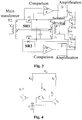
- Fig. 3 is a circuit principle diagram of synchronous rectifier driving apparatus provided by an embodiment of the present disclosure.
- the apparatus includes comparison circuits, amplification circuits and an isolated driving circuit, wherein the comparison circuits compare the magnitudes of source and drain voltages of a synchronous rectifier Metal Oxide Semiconductor (MOS) tube respectively, the amplification circuits amplify signals obtained by comparison to obtain detection signals respectively, and the isolated driving circuit generates an isolated driving signal according to the detection signals, and provides the isolated driving signal for gates and sources of a first synchronous rectifier SR1 and a second synchronous rectifier SR2.
- MOS Metal Oxide Semiconductor
- the direction of a current flowing through the synchronous rectifier MOS tube can be judged by detecting the source and drain voltages of the synchronous rectifier MOS tube, so that corresponding driving signals of the first synchronous rectifier SR1 and the second synchronous rectifier SR2 are generated.
- the first synchronous rectifier SR1 and the second synchronous rectifier SR2 perform respective half-wave rectification on a secondary side of the main transformer, and the comparison circuits and amplification circuits of the first synchronous rectifier SR1 and the second synchronous rectifier SR2 are identical.
- the comparison circuits are configured to compare the source and drain voltages of the first synchronous rectifier SR1 and the second synchronous rectifier SR2 respectively, and the comparison circuits corresponding to the first synchronous rectifier SR1 and the second synchronous rectifier SR2 are identical.
- the amplification circuits are configured to amplify signals generated by the comparison circuits of the first synchronous rectifier SR1 and the second synchronous rectifier SR2 to obtain detection signals, and the amplification circuits corresponding to the first synchronous rectifier SR1 and the second synchronous rectifier SR2 are identical.
- the isolated driving circuit is configured to output the detection signals generated by the amplification circuits of the first synchronous rectifier SR1 and the second synchronous rectifier SR2 in a push-pull way, and then the detection signals are input into first and second pins of a primary side of an isolated driving transformer T1, and two secondary windings of the isolated driving transformer perform isolated driving on gates and sources of the corresponding first synchronous rectifier SR1 and the corresponding second synchronous rectifier SR2 according to a phase relationship respectively.
- Each comparison circuit includes two triodes and two diodes. As shown in Fig. 4 or Fig. 5 , a base and collector of a triode T 1 are connected and then coupled to a drain of a synchronous rectifier MOS tube SR, an emitter of the triode T 1 is connected to a cathode of a diode D 1 , a base of a triode T 2 is coupled to a source of the synchronous rectifier MOS tube SR, a collector of the triode T 2 is coupled to an input end of the corresponding amplification circuit, an emitter of the triode T 2 is connected to a cathode of a diode D 2 , and anodes of the diode D 1 and the diode D 2 are coupled to an auxiliary power supply via a resistor R 1 .
- Each amplification circuit includes a triode, a diode and a resistor.
- an emitter of a triode T 3 is connected to a source of the synchronous rectifier MOS tube SR, a base of the triode T 3 and an anode of a diode D 3 are each connected to an output end of the corresponding comparison circuit, and a collector of the triode T 3 is connected to a cathode of the diode D 3 and is connected to the auxiliary power supply V cc via a resistor R 2 .
- each amplification circuit includes three triodes, a diode and a resistor. As shown in Fig.
- an emitter of a triode T 3 is connected to a source of the synchronous rectifier MOS tube SR, a base of the triode T 3 and an anode of a diode D 3 are connected to an output end of the corresponding comparison circuit respectively, a collector of the triode T 3 and a cathode of the diode D 3 are connected to a collector of a triode T 4 respectively, a base of the triode T 4 is connected to a base of a triode T 5 and a collector of the triode T 5 respectively and is connected to the source of the synchronous rectifier MOS tube SR via a resistor R 2 , and an emitter of the triode T 4 and an emitter of the triode T 5 are connected to the auxiliary power supply V cc .
- the isolated driving circuit includes two integrated driving chips and an isolated driving transformer, an input end of each integrated driving chip is coupled to an output end of the corresponding amplification circuit, an output end of the integrated driving chip corresponding to the first synchronous rectifier SR1 is coupled to a first pin of the isolated driving transformer T1, an output end of the integrated driving chip corresponding to the second synchronous rectifier SR2 is coupled to a second pin of the isolated driving transformer T1, third and fourth pins of the isolated driving transformer T1 are connected to the gate and source of the first synchronous rectifier SR1 respectively, and sixth and fifth pins of the isolated driving transformer T1 are connected to the gate and source of the second synchronous rectifier SR2 respectively.
- the isolated driving circuit includes two push-pull circuits and an isolated driving transformer, a triode VT7 and a triode VT8 corresponding to the first synchronous rectifier SR1 form a push-pull circuit, bases of the triode VT7 and the triode VT8 are coupled to the output end of the amplification circuit corresponding to the first synchronous rectifier SR1 respectively, and emitters of the triode VT7 and the triode VT8 are coupled to a first pin of the isolated driving transformer T1; and a triode VT9 and a triode VT10 corresponding to the second synchronous rectifier SR2 form another push-pull circuit, bases of the triode VT9 and the triode VT10 are coupled to the output end of the amplification circuit corresponding to the second synchronous rectifier SR2, emitters of the triode VT9 and the triode VT10 are coupled to a second pin of the isolated driving transformer T1, third and fourth pins of the isolated driving transformer T1 are connected to the gate and source of the
- the apparatus further includes a first parasitic diode connected between the drain and source of the first synchronous rectifier SR1, an anode of the first parasitic diode is connected to the source of the first synchronous rectifier SR1, and a cathode of the first parasitic diode is connected to the drain of the first synchronous rectifier SR1.
- the apparatus further includes a second parasitic diode connected between the drain and source of the second synchronous rectifier SR2, an anode of the second parasitic diode is connected to the source of the second synchronous rectifier SR2, and a cathode of the second parasitic diode is connected to the drain of the second synchronous rectifier SR2.
- the apparatus further includes a capacitor, one end of the capacitor is connected to a centre tap of the secondary winding of the main transformer, and the other end of the capacitor is connected to the source of the first synchronous rectifier SR1 and the source of the second synchronous rectifier SR2 respectively.
- the input ends of the each comparison circuit of the apparatus for driving the synchronous rectifier are coupled to the source and drain of the synchronous rectifier MOS tube, and the output end of the each comparison circuit is coupled to the input end of the amplification circuit; the output end of the amplification circuit is coupled to the input end of the isolated driving circuit; and outputs of the secondary side of the isolated driving transformer of the isolated driving circuit are coupled to the gates and sources of the first synchronous rectifier SR1 and the second synchronous rectifier SR2 respectively.
- the comparison circuits are configured to compare the source and drain voltages of the synchronous rectifier MOS tube, preferably, a circuit composed of an accurately-matched triode pair and an accurately-matched high-voltage diode pair is adopted, and a result reflects the direction of the current flowing through the synchronous rectifier MOS tube.
- the amplification circuit amplify the signal output by the comparison circuit.
- the isolated driving circuit is configured to generate an isolated driving signal according to an amplification result, and transmit the isolated driving signal to the gates and sources of the first synchronous rectifier SR1 and the second synchronous rectifier SR2.
- Fig. 4 is a first circuit principle diagram of a detection circuit provided by an embodiment of the present disclosure. As shown in Fig. 4 , the detection circuit includes a comparison circuit and an amplification circuit.
- the comparison circuit includes a triode T 1 , a triode T 2 , a diode D 1 and a diode D 2 .
- a base and collector of the triode T 1 are connected to a drain of a synchronous rectifier MOS tube SR, a base of the triode T 2 is connected to a source of the synchronous rectifier MOS tube SR, an emitter of the triode T 1 is connected to a cathode of the diode D 1 , an emitter of the triode T 2 is connected to a cathode of the diode D 2 , anodes of the diode D 1 and the diode D 2 are connected to an auxiliary power supply V cc via a resistor R 1 , and a collector of the triode T 2 and a base of the triode T 3 are connected to an anode of the diode D 3 .
- the amplification circuit includes a triode T 3 , a diode D 3 and a resistor R 2 .
- An emitter of the triode T 3 is connected to the source of the synchronous rectifier MOS tube SR, a base of the triode T 3 and an anode of the diode D 3 are connected to the collector of the triode T 2 , and a collector of the triode T 3 is connected to a cathode of the diode D 3 and is connected to the auxiliary power supply V cc via the resistor R 2 .
- the circuit composed of the accurately-matched triode pair T 1 and T 2 and the accurately-matched high-voltage diode pair D 1 and D 2 compares the drain and source voltages of the synchronous rectifier MOS tube SR, and transmits a signal obtained by comparison to the amplification circuit composed of the triode T 3 , the diode D 3 and the resistor R2, the signal is amplified and then is transmitted to the isolated driving circuit, and an isolated driving signal is generated by the isolated driving circuit and then is transmitted to a gate of the synchronous rectifier MOS tube SR.
- Fig. 5 is a second circuit principle diagram of a detection circuit provided by an embodiment of the present disclosure.
- the difference between the detection circuits shown by Fig. 5 and Fig. 4 is the amplification circuit.
- the amplification circuit includes a triode T 3 , a triode T 4 , a triode T 5 , a diode D 3 and a resistor R 2 .
- An emitter of the triode T 3 is connected to the source of the synchronous rectifier MOS tube SR, a base of the triode T 3 and an anode of the diode D 3 are connected to the collector of the triode T 2 respectively, a collector of the triode T 3 and a cathode of the diode D 3 are connected to a collector of the triode T 4 , a base of the triode T 4 is connected to a base of the triode T 5 and a collector of the triode T 5 respectively and is connected to the source of the synchronous rectifier MOS tube SR via the resistor R 2 , and an emitter of the triode T 4 and an emitter of the triode T 5 are connected to the auxiliary power supply V cc .
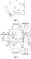
- Fig. 6 is a principle diagram of a full-bridge synchronous rectifier circuit provided by an embodiment of the present disclosure.
- the difference between the circuits shown by Fig. 6 and Fig. 3 is as follows.
- a secondary side of a main transformer T2 is a single winding
- the full-bridge synchronous rectifier circuit is composed of four synchronous rectifiers SR1, SR2, SR3 and SR4, and the isolated driving transformer is provided with four secondary windings for driving the four synchronous rectifiers respectively.
- the isolated driving transformer is provided with four secondary windings for driving the four synchronous rectifiers respectively.
- double tubes SR1 and SR2 form comparison circuits and amplification circuits
- an input end of the full-bridge synchronous rectifier circuit is connected to the single winding of the secondary side of the main transformer T2
- the drain and source voltages of the two synchronous rectifiers SR1 and SR2 on one of input branch circuits are compared by using the comparison circuits respectively
- comparison results are amplified by using the amplification circuits to obtain two detection signals corresponding to the synchronous rectifiers SR1 and SR2 respectively.
- the detection signal corresponding to the synchronous rectifier SR1 is output to a push-pull circuit composed of VT7 and VT8, the detection signal corresponding to the synchronous rectifier SR2 is output to a push-pull circuit composed of VT9 and VT10, and outputs of the two push-pull circuits are connected to first and second pins of a primary winding of the isolated driving transformer respectively.
- the secondary side of the isolated driving transformer adopts four windings.
- third and fourth pins of the isolated driving transformer T1 are connected to the gate and source of the synchronous rectifier SR1 respectively
- sixth and fifth pins of the isolated driving transformer T1 are connected to the gate and source of the synchronous rectifier SR2 respectively
- tenth and ninth pins of the isolated driving transformer T1 are connected to the gate and source of the synchronous rectifier SR3 respectively
- seventh and eighth pins of the isolated driving transformer T1 are connected to the gate and source of the synchronous rectifier SR4 respectively.
- circuits shown in Fig. 4 or Fig. 5 may be selected as the comparison circuit and the amplification circuit.
- the apparatus further includes four parasitic diodes, each parasitic diode is connected to the corresponding synchronous rectifier, an anode of each parasitic diode is connected to a source of the corresponding synchronous rectifier, and a cathode of this parasitic diode is connected to a drain of this synchronous rectifier.
- the apparatus further includes a capacitor, one end of the capacitor is connected to drains of the synchronous rectifiers SR3 and SR4 respectively, and the other end of the capacitor is connected to sources of the synchronous rectifiers SR1 and SR2 respectively.
- the direction of the current flowing through the synchronous rectifier is judged by detecting the source and drain voltages of the synchronous rectifier, so that the isolated driving signal of the corresponding synchronous rectifier is generated, thereby acquiring the isolated driving signals of the synchronous rectifier more simply and effectively.
- the apparatus and method for driving the synchronous rectifier provided by the embodiment of the present disclosure have the beneficial effects as follows.
- the direction of the current flowing through the synchronous rectifier is judged by detecting the source and drain voltages of the synchronous rectifier, so that the isolated driving signal of the corresponding synchronous rectifier is generated, thereby acquiring the isolated driving signal of the synchronous rectifier more simply and effectively.
Landscapes
- Engineering & Computer Science (AREA)
- Power Engineering (AREA)
- Rectifiers (AREA)
- Dc-Dc Converters (AREA)
Description
- The present disclosure relates to the field of power supplies for communications, and in particular to a driving apparatus for LLC resonant converter synchronous rectifier and a relevant driving method.
- In order to meet high-efficiency and high-power density requirements, a resonant converter is widely applied to a Direct Current (DC)-DC power converter. However, due to the fact that a secondary-side rectification diode may cause a quite high conduction loss, a circuit composed of rectification diodes is replaced by a rectifier circuit composed of transistors, and the rectifier circuit is applied to the resonant converter. Compared with a conversion circuit adopting the rectification diodes, the circuit adopting the transistors for rectification can reduce a power loss. A conventional synchronous rectifier control method is as follows:
- 1, a current flowing through a secondary-side synchronous rectifier parasitic diode is detected by using a current transformer, a synchronous rectifier is turned on when it is detected that the current flows, however, due to the fact that the current transformer has parasitic inductance, a current signal and a turn-on signal are likely to delay, and the current transformer is likely to be interfered, thereby increasing the cost and the size; and
- 2, a control signal of the synchronous rectifier is the same as or different from that of a main power mosfet, and a driving signal of a synchronous driving tube, serving as a control signal of the synchronous rectifier, is relatively easy to obtain, but when the synchronous rectifier works in a discontinuous current mode, the control signal of the synchronous rectifier is relatively difficult to acquire, and if a signal which is the same as or different from that of the main power mosfet is directly adopted, the problems of reverse current flowing and the like will be caused so as to seriously affect the working of the circuit.
-
CN 102263209 discloses a DC/DC power converter having active self-driving synchronous rectification.CN 101170280 discloses a setting method for self-closing of display power supply.CN 101902136 discloses a driving device and driving method for synchronous rectifying tube.EP 2200164 discloses a direct current converter power supply apparatus and method for improving direct current converter power supply apparatus. - An embodiment of the present disclosure is intended to provide apparatus and a method for driving synchronous rectifiers, which may better solve the problem how to obtain isolated driving signals of the synchronous rectifiers simply and effectively.
- According to one aspect of the embodiment of the present disclosure, apparatus for driving synchronous rectifiers is provided, which may include:
- detection circuits configured to detect drain and source voltages of the synchronous rectifiers to obtain detection signals for indicating current directions in the synchronous rectifiers;
- an isolated driving circuit configured to generate isolated driving signals for driving the synchronous rectifiers according to the detection signals output by the detection circuits; and
- the synchronous rectifiers configured to synchronously rectify input signals from a main transformer by using the isolated driving signals.
- Preferably, the apparatus may include two synchronous rectifiers, each of the two synchronous rectifiers being connected to a secondary winding of the main transformer and one of the detection circuits.
- Preferably, the isolated driving circuit may include two push-pull circuits and an isolated driving transformer, wherein
an input end of each of the two push-pull circuits may be connected to one of the detection circuits; and
a primary winding of the isolated driving transformer may be connected to output ends of the two push-pull circuits, and each of two secondary windings of the isolated driving transformer may be connected to a gate and source of one of synchronous rectifiers. - Preferably, the apparatus may include a full-bridge rectifier circuit formed by four synchronous rectifiers, input ends of the full-bridge rectifier circuit may be connected to the secondary windings of the main transformer, and a synchronous rectifier, of which the source is grounded, in the two synchronous rectifiers in each input branch circuit of the full-bridge rectifier circuit may be connected to one of the detection circuits.
- Preferably, the isolated driving circuit may include two push-pull circuits and an isolated driving transformer, wherein
an input end of each of the two push-pull circuits may be connected to the one of the detection circuit; and
a primary winding of the isolated driving transformer may be connected to output ends of the two push-pull circuits, and each of four secondary windings of the isolated driving transformer may be connected to a gate and source of the one of the synchronous rectifier. - Preferably, each of the detection circuits may include:
- a comparison circuit, an input end thereof being connected to a drain and source of the one of the synchronous rectifiers; and
- an amplification circuit, an input end thereof being connected to the comparison circuit, an output end thereof being connected to one of the two push-pull circuits.
- Preferably, the comparison circuit may include a first comparison branch circuit and a second comparison branch circuit, and one end of the first comparison branch circuit and one end of the second comparison branch circuit may be connected to an auxiliary power supply via a first resistor, wherein
the first comparison branch circuit may include: - a first triode, a base and collector thereof being connected to the drain of the one of the synchronous rectifiers;
- a first diode, a cathode thereof being connected to an emitter of the first triode, an anode thereof being connected to the first resistor;
- the second comparison branch circuit may include:
- a second triode, a base thereof being connected to the source of the one of the synchronous rectifiers, a collector thereof being connected to the amplification circuit; and
- a second diode, a cathode thereof being connected to an emitter of the second triode, an anode thereof being connected to the first resistor.
- According to another aspect of the embodiment of the present disclosure, a method for driving synchronous rectifiers is provided, which may include that:
- detection signals for indicating current directions in the synchronous rectifiers are obtained respectively by detecting drain and source voltages of the synchronous rectifiers;
- isolated driving signals for driving the synchronous rectifiers are generated according to the obtained detection signals; and
- input signals from a main transformer are synchronously rectified by using the isolated driving signals.
- Preferably, the step that the detection signals for indicating the current directions in the synchronous rectifiers are obtained may include that:
- the drain and source voltages of each of the synchronous rectifiers are compared by using a comparison circuit; and
- an output of the comparison circuit is amplified by using an amplification circuit to obtain the detection signal for indicating the current direction in the each of the synchronous rectifiers.
- Preferably, the step that the isolated driving signals for driving the synchronous rectifiers are generated may include that:
the detection signals are output to an isolated driving transformer in a push-pull way by using a push-pull circuit, in order that the isolated driving transformer generates the isolated driving signals for driving the synchronous rectifiers. - Compared with the traditional art, the embodiment of the present disclosure has beneficial effects as follows.
- The embodiment of the present disclosure can obtain the isolated driving signals of the synchronous rectifier simply and effectively, and has a superior protective feature in case of shoot-through and other abnormalities.
-
-
Fig. 1 is a block diagram of apparatus for driving synchronous rectifiers provided by an embodiment of the present disclosure; -
Fig. 2 is a principal block diagram of a method for driving synchronous rectifiers provided by an embodiment of the present disclosure; -
Fig. 3 is a circuit principle diagram of synchronous rectifier driving apparatus provided by an embodiment of the present disclosure; -
Fig. 4 is a first circuit principle diagram of a detection circuit provided by an embodiment of the present disclosure; -
Fig. 5 is a second circuit principle diagram of a detection circuit provided by an embodiment of the present disclosure; and -
Fig. 6 is a principle diagram of a full-bridge synchronous rectifier circuit provided by an embodiment of the present disclosure. - The preferred embodiments of the present disclosure are described below with reference to the drawings in detail. It should be understood that the preferred embodiments described below are only intended to describe and explain the present disclosure, and do not limit the present disclosure.
-
Fig. 1 is a block diagram of apparatus for driving synchronous rectifiers provided by an embodiment of the present disclosure. As shown inFig. 1 , the apparatus includes detection circuits, an isolated driving circuit, synchronous rectifiers and a main transformer. each detection circuit detects drain and source voltages of one of the synchronous rectifiers to obtain a detection signal for indicating a current direction in the one of the synchronous rectifiers; the isolated driving circuit generates isolated driving signals for driving the synchronous rectifiers according to the detection signals output by the detection circuits; and the synchronous rectifiers synchronously rectifies input signals from the main transformer by using the isolated driving signal. - Preferably, the main transformer of the apparatus is provided with two secondary windings.
- The apparatus includes two synchronous rectifiers, each being connected to the corresponding secondary winding of the main transformer and a detection circuit. At this time, the isolated driving circuit comprises two push-pull circuits and an isolated driving transformer, an input end of each of the two push-pull circuits is connected to a detection circuit, a primary winding of the isolated driving transformer is connected to output ends of the two push-pull circuits, and each of two secondary windings of the isolated driving transformer is connected to a gate and source of the corresponding synchronous rectifier.
- Preferably, the main transformer of the apparatus is provided with a primary winding.
- The apparatus comprises a full-bridge rectifier circuit formed by four synchronous rectifiers, input ends of the full-bridge rectifier circuit are connected to the secondary windings of the main transformer, and the synchronous rectifier, of which the sound is grounded, in the two synchronous rectifiers of each input branch circuit is connected to a detection circuit. At this time, the isolated driving circuit comprises two push-pull circuits and an isolated driving transformer, an input end of each of the two push-pull circuits is connected to a detection circuit, a primary winding of the isolated driving transformer is connected to output ends of the two push-pull circuits, and each of four secondary windings of the isolated driving transformer is connected to a gate and source of a synchronous rectifier.
- The detection circuit includes:
- a comparison circuit, an input end thereof being connected to a drain and source of the synchronous rectifier; and
- an amplification circuit, an input end thereof being connected to the comparison circuit, an output end thereof being connected to the two push-pull circuits.
- Preferably, the comparison circuit includes a first comparison branch circuit and a second comparison branch circuit, and one end of the first comparison branch circuit and one end of the second comparison branch circuit are connected to an auxiliary power supply via a first resistor, wherein
the first comparison branch circuit includes: - a first triode, a base and collector thereof being connected to the drain of the synchronous rectifier;
- a first diode, a cathode thereof being connected to an emitter of the first triode, an anode thereof being connected to the first resistor;
- the second comparison branch circuit includes:
- a second triode, a base thereof being connected to the source of the synchronous rectifier, a collector thereof being connected to the amplification circuit; and
- a second diode, a cathode thereof being connected to an emitter of the second triode, an anode thereof being connected to the first resistor.
-
Fig. 2 is a principal block diagram of a method for driving synchronous rectifiers provided by an embodiment of the present disclosure. As shown inFig. 2 , the method includes the steps as follows. - Step 201: drain and source voltages of each synchronous rectifier are detected to obtain a detection signal for indicating a current direction in the synchronous rectifier.
- The step that the detection signal for indicating the current direction in the synchronous rectifier is obtained includes that: the drain and source voltages of the synchronous rectifier are compared by using a comparison circuit; and an output of the comparison circuit is amplified by using an amplification circuit to obtain the detection signal for indicating the current direction in the synchronous rectifier.
- Step 202: an isolated driving signal for driving the synchronous rectifier is generated according to the obtained detection signal.
- The step that the isolated driving signal for driving the synchronous rectifier is generated includes that: the detection signal is output to an isolated driving transformer in a push-pull way by using a push-pull circuit, in order that the isolated driving transformer generates the isolated driving signal for driving the synchronous rectifier.
- Step 203: an input signal from a main transformer is synchronously rectified by using the isolated driving signal.
-
Fig. 3 is a circuit principle diagram of synchronous rectifier driving apparatus provided by an embodiment of the present disclosure. As shown inFig. 3 , the apparatus includes comparison circuits, amplification circuits and an isolated driving circuit, wherein the comparison circuits compare the magnitudes of source and drain voltages of a synchronous rectifier Metal Oxide Semiconductor (MOS) tube respectively, the amplification circuits amplify signals obtained by comparison to obtain detection signals respectively, and the isolated driving circuit generates an isolated driving signal according to the detection signals, and provides the isolated driving signal for gates and sources of a first synchronous rectifier SR1 and a second synchronous rectifier SR2. The direction of a current flowing through the synchronous rectifier MOS tube can be judged by detecting the source and drain voltages of the synchronous rectifier MOS tube, so that corresponding driving signals of the first synchronous rectifier SR1 and the second synchronous rectifier SR2 are generated. - Specifically, the first synchronous rectifier SR1 and the second synchronous rectifier SR2 perform respective half-wave rectification on a secondary side of the main transformer, and the comparison circuits and amplification circuits of the first synchronous rectifier SR1 and the second synchronous rectifier SR2 are identical. The comparison circuits are configured to compare the source and drain voltages of the first synchronous rectifier SR1 and the second synchronous rectifier SR2 respectively, and the comparison circuits corresponding to the first synchronous rectifier SR1 and the second synchronous rectifier SR2 are identical. The amplification circuits are configured to amplify signals generated by the comparison circuits of the first synchronous rectifier SR1 and the second synchronous rectifier SR2 to obtain detection signals, and the amplification circuits corresponding to the first synchronous rectifier SR1 and the second synchronous rectifier SR2 are identical. The isolated driving circuit is configured to output the detection signals generated by the amplification circuits of the first synchronous rectifier SR1 and the second synchronous rectifier SR2 in a push-pull way, and then the detection signals are input into first and second pins of a primary side of an isolated driving transformer T1, and two secondary windings of the isolated driving transformer perform isolated driving on gates and sources of the corresponding first synchronous rectifier SR1 and the corresponding second synchronous rectifier SR2 according to a phase relationship respectively.
- Each comparison circuit includes two triodes and two diodes. As shown in
Fig. 4 orFig. 5 , a base and collector of a triode T1 are connected and then coupled to a drain of a synchronous rectifier MOS tube SR, an emitter of the triode T1 is connected to a cathode of a diode D1, a base of a triode T2 is coupled to a source of the synchronous rectifier MOS tube SR, a collector of the triode T2 is coupled to an input end of the corresponding amplification circuit, an emitter of the triode T2 is connected to a cathode of a diode D2, and anodes of the diode D1 and the diode D2 are coupled to an auxiliary power supply via a resistor R1. - Each amplification circuit includes a triode, a diode and a resistor. As shown in
Fig. 4 , an emitter of a triode T3 is connected to a source of the synchronous rectifier MOS tube SR, a base of the triode T3 and an anode of a diode D3 are each connected to an output end of the corresponding comparison circuit, and a collector of the triode T3 is connected to a cathode of the diode D3 and is connected to the auxiliary power supply Vcc via a resistor R2. Or, each amplification circuit includes three triodes, a diode and a resistor. As shown inFig. 5 , an emitter of a triode T3 is connected to a source of the synchronous rectifier MOS tube SR, a base of the triode T3 and an anode of a diode D3 are connected to an output end of the corresponding comparison circuit respectively, a collector of the triode T3 and a cathode of the diode D3 are connected to a collector of a triode T4 respectively, a base of the triode T4 is connected to a base of a triode T5 and a collector of the triode T5 respectively and is connected to the source of the synchronous rectifier MOS tube SR via a resistor R2, and an emitter of the triode T4 and an emitter of the triode T5 are connected to the auxiliary power supply Vcc. - The isolated driving circuit includes two integrated driving chips and an isolated driving transformer, an input end of each integrated driving chip is coupled to an output end of the corresponding amplification circuit, an output end of the integrated driving chip corresponding to the first synchronous rectifier SR1 is coupled to a first pin of the isolated driving transformer T1, an output end of the integrated driving chip corresponding to the second synchronous rectifier SR2 is coupled to a second pin of the isolated driving transformer T1, third and fourth pins of the isolated driving transformer T1 are connected to the gate and source of the first synchronous rectifier SR1 respectively, and sixth and fifth pins of the isolated driving transformer T1 are connected to the gate and source of the second synchronous rectifier SR2 respectively. Or, the isolated driving circuit includes two push-pull circuits and an isolated driving transformer, a triode VT7 and a triode VT8 corresponding to the first synchronous rectifier SR1 form a push-pull circuit, bases of the triode VT7 and the triode VT8 are coupled to the output end of the amplification circuit corresponding to the first synchronous rectifier SR1 respectively, and emitters of the triode VT7 and the triode VT8 are coupled to a first pin of the isolated driving transformer T1; and a triode VT9 and a triode VT10 corresponding to the second synchronous rectifier SR2 form another push-pull circuit, bases of the triode VT9 and the triode VT10 are coupled to the output end of the amplification circuit corresponding to the second synchronous rectifier SR2, emitters of the triode VT9 and the triode VT10 are coupled to a second pin of the isolated driving transformer T1, third and fourth pins of the isolated driving transformer T1 are connected to the gate and source of the first synchronous rectifier SR1 respectively, and sixth and fifth pins of the isolated driving transformer T1 are connected to the gate and source of the second synchronous rectifier SR2 respectively.
- Preferably, the apparatus further includes a first parasitic diode connected between the drain and source of the first synchronous rectifier SR1, an anode of the first parasitic diode is connected to the source of the first synchronous rectifier SR1, and a cathode of the first parasitic diode is connected to the drain of the first synchronous rectifier SR1. The apparatus further includes a second parasitic diode connected between the drain and source of the second synchronous rectifier SR2, an anode of the second parasitic diode is connected to the source of the second synchronous rectifier SR2, and a cathode of the second parasitic diode is connected to the drain of the second synchronous rectifier SR2. The apparatus further includes a capacitor, one end of the capacitor is connected to a centre tap of the secondary winding of the main transformer, and the other end of the capacitor is connected to the source of the first synchronous rectifier SR1 and the source of the second synchronous rectifier SR2 respectively.
- As mentioned above, the input ends of the each comparison circuit of the apparatus for driving the synchronous rectifier are coupled to the source and drain of the synchronous rectifier MOS tube, and the output end of the each comparison circuit is coupled to the input end of the amplification circuit; the output end of the amplification circuit is coupled to the input end of the isolated driving circuit; and outputs of the secondary side of the isolated driving transformer of the isolated driving circuit are coupled to the gates and sources of the first synchronous rectifier SR1 and the second synchronous rectifier SR2 respectively. The comparison circuits are configured to compare the source and drain voltages of the synchronous rectifier MOS tube, preferably, a circuit composed of an accurately-matched triode pair and an accurately-matched high-voltage diode pair is adopted, and a result reflects the direction of the current flowing through the synchronous rectifier MOS tube. The amplification circuit amplify the signal output by the comparison circuit. The isolated driving circuit is configured to generate an isolated driving signal according to an amplification result, and transmit the isolated driving signal to the gates and sources of the first synchronous rectifier SR1 and the second synchronous rectifier SR2.
-
Fig. 4 is a first circuit principle diagram of a detection circuit provided by an embodiment of the present disclosure. As shown inFig. 4 , the detection circuit includes a comparison circuit and an amplification circuit. - The comparison circuit includes a triode T1, a triode T2, a diode D1 and a diode D2. A base and collector of the triode T1 are connected to a drain of a synchronous rectifier MOS tube SR, a base of the triode T2 is connected to a source of the synchronous rectifier MOS tube SR, an emitter of the triode T1 is connected to a cathode of the diode D1, an emitter of the triode T2 is connected to a cathode of the diode D2, anodes of the diode D1 and the diode D2 are connected to an auxiliary power supply Vcc via a resistor R1, and a collector of the triode T2 and a base of the triode T3 are connected to an anode of the diode D3.
- The amplification circuit includes a triode T3, a diode D3 and a resistor R2. An emitter of the triode T3 is connected to the source of the synchronous rectifier MOS tube SR, a base of the triode T3 and an anode of the diode D3 are connected to the collector of the triode T2, and a collector of the triode T3 is connected to a cathode of the diode D3 and is connected to the auxiliary power supply Vcc via the resistor R2.
- The circuit composed of the accurately-matched triode pair T1 and T2 and the accurately-matched high-voltage diode pair D1 and D2 compares the drain and source voltages of the synchronous rectifier MOS tube SR, and transmits a signal obtained by comparison to the amplification circuit composed of the triode T3, the diode D3 and the resistor R2, the signal is amplified and then is transmitted to the isolated driving circuit, and an isolated driving signal is generated by the isolated driving circuit and then is transmitted to a gate of the synchronous rectifier MOS tube SR.
-
Fig. 5 is a second circuit principle diagram of a detection circuit provided by an embodiment of the present disclosure. The difference between the detection circuits shown byFig. 5 andFig. 4 is the amplification circuit. As shown inFig. 5 , the amplification circuit includes a triode T3, a triode T4, a triode T5, a diode D3 and a resistor R2. An emitter of the triode T3 is connected to the source of the synchronous rectifier MOS tube SR, a base of the triode T3 and an anode of the diode D3 are connected to the collector of the triode T2 respectively, a collector of the triode T3 and a cathode of the diode D3 are connected to a collector of the triode T4, a base of the triode T4 is connected to a base of the triode T5 and a collector of the triode T5 respectively and is connected to the source of the synchronous rectifier MOS tube SR via the resistor R2, and an emitter of the triode T4 and an emitter of the triode T5 are connected to the auxiliary power supply Vcc. -
Fig. 6 is a principle diagram of a full-bridge synchronous rectifier circuit provided by an embodiment of the present disclosure. The difference between the circuits shown byFig. 6 andFig. 3 is as follows. In the embodiment, a secondary side of a main transformer T2 is a single winding, the full-bridge synchronous rectifier circuit is composed of four synchronous rectifiers SR1, SR2, SR3 and SR4, and the isolated driving transformer is provided with four secondary windings for driving the four synchronous rectifiers respectively. As shown inFig. 6 , in the embodiment, double tubes SR1 and SR2 form comparison circuits and amplification circuits, an input end of the full-bridge synchronous rectifier circuit is connected to the single winding of the secondary side of the main transformer T2, the drain and source voltages of the two synchronous rectifiers SR1 and SR2 on one of input branch circuits are compared by using the comparison circuits respectively, and comparison results are amplified by using the amplification circuits to obtain two detection signals corresponding to the synchronous rectifiers SR1 and SR2 respectively. The detection signal corresponding to the synchronous rectifier SR1 is output to a push-pull circuit composed of VT7 and VT8, the detection signal corresponding to the synchronous rectifier SR2 is output to a push-pull circuit composed of VT9 and VT10, and outputs of the two push-pull circuits are connected to first and second pins of a primary winding of the isolated driving transformer respectively. The secondary side of the isolated driving transformer adopts four windings. According to polarity situations of primary and secondary sides, third and fourth pins of the isolated driving transformer T1 are connected to the gate and source of the synchronous rectifier SR1 respectively, sixth and fifth pins of the isolated driving transformer T1 are connected to the gate and source of the synchronous rectifier SR2 respectively, tenth and ninth pins of the isolated driving transformer T1 are connected to the gate and source of the synchronous rectifier SR3 respectively, and seventh and eighth pins of the isolated driving transformer T1 are connected to the gate and source of the synchronous rectifier SR4 respectively. - The circuits shown in
Fig. 4 orFig. 5 may be selected as the comparison circuit and the amplification circuit. - Preferably, the apparatus further includes four parasitic diodes, each parasitic diode is connected to the corresponding synchronous rectifier, an anode of each parasitic diode is connected to a source of the corresponding synchronous rectifier, and a cathode of this parasitic diode is connected to a drain of this synchronous rectifier. The apparatus further includes a capacitor, one end of the capacitor is connected to drains of the synchronous rectifiers SR3 and SR4 respectively, and the other end of the capacitor is connected to sources of the synchronous rectifiers SR1 and SR2 respectively.
- As mentioned above, in the embodiment of the present disclosure, the direction of the current flowing through the synchronous rectifier is judged by detecting the source and drain voltages of the synchronous rectifier, so that the isolated driving signal of the corresponding synchronous rectifier is generated, thereby acquiring the isolated driving signals of the synchronous rectifier more simply and effectively.
- Although the present disclosure is described above in detail, the present disclosure is not limited thereto. Those skilled in the art can make various modifications according to the principle of the present disclosure. Thus, the modifications made according to the principle of the present disclosure shall fall within the protection scope of the present disclosure.
- As mentioned above, the apparatus and method for driving the synchronous rectifier provided by the embodiment of the present disclosure have the beneficial effects as follows. In the embodiment of the present disclosure, the direction of the current flowing through the synchronous rectifier is judged by detecting the source and drain voltages of the synchronous rectifier, so that the isolated driving signal of the corresponding synchronous rectifier is generated, thereby acquiring the isolated driving signal of the synchronous rectifier more simply and effectively.
Claims (10)
- Apparatus for driving synchronous rectifiers (SR1, SR2, SR3, SR4), characterized in that it comprises:detection circuits, wherein each of the detection circuits is configured to detect drain and source voltages of one of the synchronous rectifiers (SR1, SR2, SR3, SR4)to obtain a detection signal for indicating a current direction in the one of the synchronous rectifiers (SR1, SR2, SR3, SR4);an isolated driving circuit configured to generate isolated driving signals for driving the synchronous rectifiers (SR1, SR2, SR3, SR4) according to the detection signals output by the detection circuits; andthe synchronous rectifiers (SR1, SR2, SR3, SR4) configured to synchronously rectify input signals from a main transformer by using the isolated driving signals.
- The apparatus according to claim 1, wherein the apparatus comprises two synchronous rectifiers (SR1, SR2), each of the two synchronous rectifiers being connected to a secondary winding of the main transformer and one of the detection circuits respectively.
- The apparatus according to claim 2, wherein the isolated driving circuit comprises two push-pull circuits and an isolated driving transformer, wherein
an input end of each of the two push-pull circuits is connected to one of the detection circuits; and
a primary winding of the isolated driving transformer is connected to output ends of the two push-pull circuits, and each of two secondary windings of the isolated driving transformer is connected to a gate and source of one of the two synchronous rectifiers (SR1, SR2). - The apparatus according to claim 1, wherein the apparatus comprises a full-bridge rectifier circuit formed by four synchronous rectifiers (SR1, SR2, SR3, SR4); input ends of the full-bridge rectifier circuit are connected to the secondary windings of the main transformer; and a synchronous rectifier, of which the source is grounded, in the two synchronous rectifiers in each input branch circuit of the full-bridge rectifier circuit is connected to one of the detection circuits.
- The apparatus according to claim 4, wherein the isolated driving circuit comprises two push-pull circuits and an isolated driving transformer, wherein
an input end of each of the two push-pull circuits is connected to the one of the detection circuits; and
a primary winding of the isolated driving transformer is connected to output ends of the two push-pull circuits, and each of four secondary windings of the isolated driving transformer is connected to a gate and source of the one of the synchronous rectifiers. - The apparatus according to claim 3 or 5, wherein each of the detection circuits comprise:a comparison circuit, wherein an input end of the comparison circuit is connected to a drain and source of the one of the synchronous rectifiers; andan amplification circuit, wherein an input end of the amplification circuit is connected to the comparison circuit, an output end of the amplification circuit is connected to one of the two push-pull circuits.
- The apparatus according to claim 6, wherein each of the comparison circuits comprises a first comparison branch circuit and a second comparison branch circuit; one end of the first comparison branch circuit and one end of the second comparison branch circuit are connected to an auxiliary power supply via a first resisto R1r;
the first comparison branch circuit comprises:a first triode T1, wherein a base and collector of the first triode T1 are connected to the drain of the one of the synchronous rectifiers;a first diode D1, wherein a cathode of the first diode D1 is connected to an emitter of the first triode T1, an anode of the first diode D1 is connected to the first resistor R1;the second comparison branch circuit comprises:a second triode T2, wherein a base of the second triode T2 is connected to the source of the one of the synchronous rectifiers, a collector of the second triode T2 is connected to the amplification circuit; anda second diode D2, wherein a cathode of the second diode D2 is connected to an emitter of the second triode T2, an anode of the second diode D2 is connected to the first resistor R1. - A method for driving synchronous rectifiers, characterized in that it comprises:• [201] detecting drain and source voltages of each of the synchronous rectifiers (SR1, SR2, SR3, SR4) to obtain detection signals for indicating current directions in the synchronous rectifiers;• [202] generating isolated driving signals for driving the synchronous rectifiers (SR1, SR2, SR3, SR4) according to the obtained detection signals; and• [203] synchronously rectifying input signals from a main transformer by using the isolated driving signals.
- The method according to claim 8, wherein obtaining the detection signals for indicating the current directions in the synchronous rectifiers (SR1, SR2, SR3, SR4) comprises:comparing the drain and source voltages of one of the synchronous rectifiers (SR1, SR2, SR3, SR4) by using a comparison circuit; andamplifying an output of the comparison circuit by using an amplification circuit to obtain the detection signal for indicating the current direction in the one of the synchronous rectifiers (SR1, SR2, SR3, SR4).
- The method according to claim 8 or 9, wherein generating the isolated driving signals for driving the synchronous rectifiers comprises (SR1, SR2, SR3, SR4):
outputting the detection signals to an isolated driving transformer in a push-pull way by using a push-pull circuit, in order that the isolated driving transformer generates the isolated driving signals for driving the synchronous rectifiers (SR1, SR2, SR3, SR4).
Applications Claiming Priority (2)
| Application Number | Priority Date | Filing Date | Title |
|---|---|---|---|
| CN201310395156.XA CN104426397A (en) | 2013-09-03 | 2013-09-03 | Driving device and method for synchronous rectifier tube |
| PCT/CN2014/076975 WO2014180314A1 (en) | 2013-09-03 | 2014-05-07 | Synchronous rectifier tube driving apparatus and method |
Publications (3)
| Publication Number | Publication Date |
|---|---|
| EP3043463A1 EP3043463A1 (en) | 2016-07-13 |
| EP3043463A4 EP3043463A4 (en) | 2016-11-02 |
| EP3043463B1 true EP3043463B1 (en) | 2018-10-17 |
Family
ID=51866728
Family Applications (1)
| Application Number | Title | Priority Date | Filing Date |
|---|---|---|---|
| EP14794972.1A Active EP3043463B1 (en) | 2013-09-03 | 2014-05-07 | Synchronous rectifier tube driving apparatus and method |
Country Status (4)
| Country | Link |
|---|---|
| US (1) | US9991807B2 (en) |
| EP (1) | EP3043463B1 (en) |
| CN (1) | CN104426397A (en) |
| WO (1) | WO2014180314A1 (en) |
Families Citing this family (10)
| Publication number | Priority date | Publication date | Assignee | Title |
|---|---|---|---|---|
| CN104703356B (en) * | 2015-03-23 | 2017-08-15 | 深圳市稳先微电子有限公司 | A kind of non-isolated voltage-dropping type LED drive circuit of intelligent synchronization rectification |
| CN105307305B (en) * | 2015-11-18 | 2017-12-19 | 深圳创维-Rgb电子有限公司 | A kind of LED power control device and television set |
| US10063159B1 (en) | 2017-06-30 | 2018-08-28 | Dialog Semiconductor Inc. | Adaptive synchronous rectifier sensing deglitch |
| US10256744B2 (en) | 2017-09-12 | 2019-04-09 | Infineon Technologies Austria Ag | Controller device with adaptive synchronous rectification |
| CN110492768A (en) * | 2019-08-13 | 2019-11-22 | 苏州格远电气有限公司 | Rectifier circuit |
| US12074516B2 (en) * | 2020-01-31 | 2024-08-27 | Panasonic Intellectual Property Management Co., Ltd. | Class-D power converter |
| US11621645B2 (en) * | 2020-06-04 | 2023-04-04 | Stmicroelectronics International N.V. | Methods and device to drive a transistor for synchronous rectification |
| CN113472206A (en) * | 2021-05-25 | 2021-10-01 | 中国电子科技集团公司第四十一研究所 | Self-driven synchronous rectification circuit |
| CN114337282B (en) * | 2021-12-30 | 2024-12-13 | 上海易咖智车科技有限公司 | A vehicle and a switch control circuit thereof |
| CN117081407A (en) * | 2022-11-21 | 2023-11-17 | 南京户能电子科技有限公司 | An adaptive synchronous rectification circuit |
Family Cites Families (8)
| Publication number | Priority date | Publication date | Assignee | Title |
|---|---|---|---|---|
| US20060002160A1 (en) * | 2004-07-01 | 2006-01-05 | Nalbant Mehmet K | Secondary side synchronous rectifier driver integrated circuits with adaptive turn-off for transformer coupled power supplies |
| US7269038B2 (en) * | 2005-09-12 | 2007-09-11 | Fairchild Semiconductor Corporation | Vrms and rectified current sense full-bridge synchronous-rectification integrated with PFC |
| CN101399498B (en) | 2007-09-26 | 2013-08-28 | 华为技术有限公司 | DC conversion power source device and method for improving DC conversion power source device |
| CN101170280B (en) * | 2007-10-17 | 2010-06-02 | 吴壬华 | A realization method of switching tube drive circuit and its circuit |
| CN102217181B (en) * | 2008-11-14 | 2014-09-03 | 伟创力国际美国公司 | Driver for a synchronous rectifier and power converter employing the same |
| CN101527525A (en) * | 2009-04-08 | 2009-09-09 | 李成勇 | Synchronous rectification external drive proposal |
| CN101902136B (en) * | 2009-05-26 | 2013-07-31 | 艾默生网络能源系统北美公司 | Driving device and driving method for synchronous rectifying tube |
| US20110286245A1 (en) * | 2010-05-24 | 2011-11-24 | Intersil Americas Inc. | Dc/dc power converter having active self driving synchronous rectification |
-
2013
- 2013-09-03 CN CN201310395156.XA patent/CN104426397A/en active Pending
-
2014
- 2014-05-07 US US14/916,086 patent/US9991807B2/en active Active
- 2014-05-07 EP EP14794972.1A patent/EP3043463B1/en active Active
- 2014-05-07 WO PCT/CN2014/076975 patent/WO2014180314A1/en not_active Ceased
Also Published As
| Publication number | Publication date |
|---|---|
| CN104426397A (en) | 2015-03-18 |
| EP3043463A1 (en) | 2016-07-13 |
| EP3043463A4 (en) | 2016-11-02 |
| WO2014180314A1 (en) | 2014-11-13 |
| US9991807B2 (en) | 2018-06-05 |
| US20160218634A1 (en) | 2016-07-28 |
Similar Documents
| Publication | Publication Date | Title |
|---|---|---|
| US9991807B2 (en) | Apparatus and method for driving synchronous rectifier | |
| CN105846695B (en) | Self-power supply for synchronous rectifiers | |
| US9866100B2 (en) | Dynamic sharing average current mode control for active-reset and self-driven synchronous rectification for power converters | |
| US8369118B2 (en) | Synchronous rectifying drive circuit with energy feedback for voltage doubler rectifer | |
| CN101902136B (en) | Driving device and driving method for synchronous rectifying tube | |
| US8243475B2 (en) | Resonance converting apparatus and synchronous rectification circuit | |
| US8077481B2 (en) | Primary sampling current controlled synchronous rectifying drive circuit | |
| TWI448064B (en) | Smart driver for flyback converts | |
| CN106300921B (en) | Synchronous rectifier tube driving method, synchronous rectifier tube circuit and switching power supply | |
| CN113809926A (en) | Synchronous rectification control circuit | |
| CN103795257A (en) | Synchronous rectifier circuit | |
| CN101488719B (en) | Synchronous rectifying driver circuit suitable for voltage-multiplying rectifying | |
| US10432187B2 (en) | Coupling structure of gate driver in power supply device | |
| EP1551097A1 (en) | Power conversion device with synchronous rectifier driving and voltage oscillation limitation during a discontinuous operating mode | |
| CN108667304A (en) | Synchronous rectification inverse-excitation type DC-DC power conversion equipment and control method | |
| CN105207457A (en) | Synchronous rectification circuit and LLC resonance converter possessing the synchronous rectification circuit | |
| CN102263509A (en) | DC/DC Power Converter with Active Self-Driven Synchronous Rectification | |
| CN201466997U (en) | A current control synchronous rectification drive circuit | |
| CN111193410B (en) | Synchronous rectifying tube control circuit, voltage conversion circuit and control method thereof | |
| US20240128884A1 (en) | Switching control unit, electric power conversion apparatus, and electric power supply system | |
| CN216056818U (en) | Synchronous rectification control circuit | |
| CN103051214A (en) | Synchronous rectifier driving circuit, operating method thereof and power converter merged into synchronous rectifier driving circuit and operating method | |
| KR101287803B1 (en) | Synchronize rectifier driver circuit for llc resonant half bridge converter and driving method thereof | |
| CN114301304B (en) | Control method and control circuit of synchronous rectifying tube and switching power supply circuit | |
| CN201466998U (en) | Synchronous rectification driving circuit suitable for voltage doubler rectification |
Legal Events
| Date | Code | Title | Description |
|---|---|---|---|
| PUAI | Public reference made under article 153(3) epc to a published international application that has entered the european phase |
Free format text: ORIGINAL CODE: 0009012 |
|
| 17P | Request for examination filed |
Effective date: 20160331 |
|
| AK | Designated contracting states |
Kind code of ref document: A1 Designated state(s): AL AT BE BG CH CY CZ DE DK EE ES FI FR GB GR HR HU IE IS IT LI LT LU LV MC MK MT NL NO PL PT RO RS SE SI SK SM TR |
|
| AX | Request for extension of the european patent |
Extension state: BA ME |
|
| A4 | Supplementary search report drawn up and despatched |
Effective date: 20160930 |
|
| RIC1 | Information provided on ipc code assigned before grant |
Ipc: H02M 7/217 20060101AFI20160926BHEP |
|
| DAX | Request for extension of the european patent (deleted) | ||
| GRAP | Despatch of communication of intention to grant a patent |
Free format text: ORIGINAL CODE: EPIDOSNIGR1 |
|
| STAA | Information on the status of an ep patent application or granted ep patent |
Free format text: STATUS: GRANT OF PATENT IS INTENDED |
|
| GRAJ | Information related to disapproval of communication of intention to grant by the applicant or resumption of examination proceedings by the epo deleted |
Free format text: ORIGINAL CODE: EPIDOSDIGR1 |
|
| GRAP | Despatch of communication of intention to grant a patent |
Free format text: ORIGINAL CODE: EPIDOSNIGR1 |
|
| GRAJ | Information related to disapproval of communication of intention to grant by the applicant or resumption of examination proceedings by the epo deleted |
Free format text: ORIGINAL CODE: EPIDOSDIGR1 |
|
| INTG | Intention to grant announced |
Effective date: 20180319 |
|
| GRAP | Despatch of communication of intention to grant a patent |
Free format text: ORIGINAL CODE: EPIDOSNIGR1 |
|
| GRAJ | Information related to disapproval of communication of intention to grant by the applicant or resumption of examination proceedings by the epo deleted |
Free format text: ORIGINAL CODE: EPIDOSDIGR1 |
|
| INTG | Intention to grant announced |
Effective date: 20180328 |
|
| GRAP | Despatch of communication of intention to grant a patent |
Free format text: ORIGINAL CODE: EPIDOSNIGR1 |
|
| INTG | Intention to grant announced |
Effective date: 20180412 |
|
| INTG | Intention to grant announced |
Effective date: 20180423 |
|
| INTG | Intention to grant announced |
Effective date: 20180503 |
|
| GRAS | Grant fee paid |
Free format text: ORIGINAL CODE: EPIDOSNIGR3 |
|
| GRAA | (expected) grant |
Free format text: ORIGINAL CODE: 0009210 |
|
| STAA | Information on the status of an ep patent application or granted ep patent |
Free format text: STATUS: THE PATENT HAS BEEN GRANTED |
|
| AK | Designated contracting states |
Kind code of ref document: B1 Designated state(s): AL AT BE BG CH CY CZ DE DK EE ES FI FR GB GR HR HU IE IS IT LI LT LU LV MC MK MT NL NO PL PT RO RS SE SI SK SM TR |
|
| REG | Reference to a national code |
Ref country code: GB Ref legal event code: FG4D |
|
| REG | Reference to a national code |
Ref country code: CH Ref legal event code: EP |
|
| REG | Reference to a national code |
Ref country code: IE Ref legal event code: FG4D |
|
| REG | Reference to a national code |
Ref country code: DE Ref legal event code: R096 Ref document number: 602014034333 Country of ref document: DE Ref country code: AT Ref legal event code: REF Ref document number: 1055158 Country of ref document: AT Kind code of ref document: T Effective date: 20181115 |
|
| REG | Reference to a national code |
Ref country code: NL Ref legal event code: MP Effective date: 20181017 |
|
| REG | Reference to a national code |
Ref country code: LT Ref legal event code: MG4D |
|
| REG | Reference to a national code |
Ref country code: AT Ref legal event code: MK05 Ref document number: 1055158 Country of ref document: AT Kind code of ref document: T Effective date: 20181017 |
|
| PG25 | Lapsed in a contracting state [announced via postgrant information from national office to epo] |
Ref country code: NL Free format text: LAPSE BECAUSE OF FAILURE TO SUBMIT A TRANSLATION OF THE DESCRIPTION OR TO PAY THE FEE WITHIN THE PRESCRIBED TIME-LIMIT Effective date: 20181017 |
|
| PG25 | Lapsed in a contracting state [announced via postgrant information from national office to epo] |
Ref country code: NO Free format text: LAPSE BECAUSE OF FAILURE TO SUBMIT A TRANSLATION OF THE DESCRIPTION OR TO PAY THE FEE WITHIN THE PRESCRIBED TIME-LIMIT Effective date: 20190117 Ref country code: LT Free format text: LAPSE BECAUSE OF FAILURE TO SUBMIT A TRANSLATION OF THE DESCRIPTION OR TO PAY THE FEE WITHIN THE PRESCRIBED TIME-LIMIT Effective date: 20181017 Ref country code: FI Free format text: LAPSE BECAUSE OF FAILURE TO SUBMIT A TRANSLATION OF THE DESCRIPTION OR TO PAY THE FEE WITHIN THE PRESCRIBED TIME-LIMIT Effective date: 20181017 Ref country code: IS Free format text: LAPSE BECAUSE OF FAILURE TO SUBMIT A TRANSLATION OF THE DESCRIPTION OR TO PAY THE FEE WITHIN THE PRESCRIBED TIME-LIMIT Effective date: 20190217 Ref country code: ES Free format text: LAPSE BECAUSE OF FAILURE TO SUBMIT A TRANSLATION OF THE DESCRIPTION OR TO PAY THE FEE WITHIN THE PRESCRIBED TIME-LIMIT Effective date: 20181017 Ref country code: LV Free format text: LAPSE BECAUSE OF FAILURE TO SUBMIT A TRANSLATION OF THE DESCRIPTION OR TO PAY THE FEE WITHIN THE PRESCRIBED TIME-LIMIT Effective date: 20181017 Ref country code: BG Free format text: LAPSE BECAUSE OF FAILURE TO SUBMIT A TRANSLATION OF THE DESCRIPTION OR TO PAY THE FEE WITHIN THE PRESCRIBED TIME-LIMIT Effective date: 20190117 Ref country code: HR Free format text: LAPSE BECAUSE OF FAILURE TO SUBMIT A TRANSLATION OF THE DESCRIPTION OR TO PAY THE FEE WITHIN THE PRESCRIBED TIME-LIMIT Effective date: 20181017 Ref country code: PL Free format text: LAPSE BECAUSE OF FAILURE TO SUBMIT A TRANSLATION OF THE DESCRIPTION OR TO PAY THE FEE WITHIN THE PRESCRIBED TIME-LIMIT Effective date: 20181017 Ref country code: AT Free format text: LAPSE BECAUSE OF FAILURE TO SUBMIT A TRANSLATION OF THE DESCRIPTION OR TO PAY THE FEE WITHIN THE PRESCRIBED TIME-LIMIT Effective date: 20181017 |
|
| PG25 | Lapsed in a contracting state [announced via postgrant information from national office to epo] |
Ref country code: PT Free format text: LAPSE BECAUSE OF FAILURE TO SUBMIT A TRANSLATION OF THE DESCRIPTION OR TO PAY THE FEE WITHIN THE PRESCRIBED TIME-LIMIT Effective date: 20190217 Ref country code: RS Free format text: LAPSE BECAUSE OF FAILURE TO SUBMIT A TRANSLATION OF THE DESCRIPTION OR TO PAY THE FEE WITHIN THE PRESCRIBED TIME-LIMIT Effective date: 20181017 Ref country code: GR Free format text: LAPSE BECAUSE OF FAILURE TO SUBMIT A TRANSLATION OF THE DESCRIPTION OR TO PAY THE FEE WITHIN THE PRESCRIBED TIME-LIMIT Effective date: 20190118 Ref country code: AL Free format text: LAPSE BECAUSE OF FAILURE TO SUBMIT A TRANSLATION OF THE DESCRIPTION OR TO PAY THE FEE WITHIN THE PRESCRIBED TIME-LIMIT Effective date: 20181017 Ref country code: SE Free format text: LAPSE BECAUSE OF FAILURE TO SUBMIT A TRANSLATION OF THE DESCRIPTION OR TO PAY THE FEE WITHIN THE PRESCRIBED TIME-LIMIT Effective date: 20181017 |
|
| REG | Reference to a national code |
Ref country code: DE Ref legal event code: R097 Ref document number: 602014034333 Country of ref document: DE |
|
| PG25 | Lapsed in a contracting state [announced via postgrant information from national office to epo] |
Ref country code: IT Free format text: LAPSE BECAUSE OF FAILURE TO SUBMIT A TRANSLATION OF THE DESCRIPTION OR TO PAY THE FEE WITHIN THE PRESCRIBED TIME-LIMIT Effective date: 20181017 Ref country code: DK Free format text: LAPSE BECAUSE OF FAILURE TO SUBMIT A TRANSLATION OF THE DESCRIPTION OR TO PAY THE FEE WITHIN THE PRESCRIBED TIME-LIMIT Effective date: 20181017 Ref country code: CZ Free format text: LAPSE BECAUSE OF FAILURE TO SUBMIT A TRANSLATION OF THE DESCRIPTION OR TO PAY THE FEE WITHIN THE PRESCRIBED TIME-LIMIT Effective date: 20181017 |
|
| PLBE | No opposition filed within time limit |
Free format text: ORIGINAL CODE: 0009261 |
|
| STAA | Information on the status of an ep patent application or granted ep patent |
Free format text: STATUS: NO OPPOSITION FILED WITHIN TIME LIMIT |
|
| PG25 | Lapsed in a contracting state [announced via postgrant information from national office to epo] |
Ref country code: SK Free format text: LAPSE BECAUSE OF FAILURE TO SUBMIT A TRANSLATION OF THE DESCRIPTION OR TO PAY THE FEE WITHIN THE PRESCRIBED TIME-LIMIT Effective date: 20181017 Ref country code: RO Free format text: LAPSE BECAUSE OF FAILURE TO SUBMIT A TRANSLATION OF THE DESCRIPTION OR TO PAY THE FEE WITHIN THE PRESCRIBED TIME-LIMIT Effective date: 20181017 Ref country code: EE Free format text: LAPSE BECAUSE OF FAILURE TO SUBMIT A TRANSLATION OF THE DESCRIPTION OR TO PAY THE FEE WITHIN THE PRESCRIBED TIME-LIMIT Effective date: 20181017 Ref country code: SM Free format text: LAPSE BECAUSE OF FAILURE TO SUBMIT A TRANSLATION OF THE DESCRIPTION OR TO PAY THE FEE WITHIN THE PRESCRIBED TIME-LIMIT Effective date: 20181017 |
|
| 26N | No opposition filed |
Effective date: 20190718 |
|
| PG25 | Lapsed in a contracting state [announced via postgrant information from national office to epo] |
Ref country code: SI Free format text: LAPSE BECAUSE OF FAILURE TO SUBMIT A TRANSLATION OF THE DESCRIPTION OR TO PAY THE FEE WITHIN THE PRESCRIBED TIME-LIMIT Effective date: 20181017 |
|
| REG | Reference to a national code |
Ref country code: CH Ref legal event code: PL |
|
| PG25 | Lapsed in a contracting state [announced via postgrant information from national office to epo] |
Ref country code: MC Free format text: LAPSE BECAUSE OF FAILURE TO SUBMIT A TRANSLATION OF THE DESCRIPTION OR TO PAY THE FEE WITHIN THE PRESCRIBED TIME-LIMIT Effective date: 20181017 Ref country code: CH Free format text: LAPSE BECAUSE OF NON-PAYMENT OF DUE FEES Effective date: 20190531 Ref country code: LI Free format text: LAPSE BECAUSE OF NON-PAYMENT OF DUE FEES Effective date: 20190531 |
|
| REG | Reference to a national code |
Ref country code: BE Ref legal event code: MM Effective date: 20190531 |
|
| PG25 | Lapsed in a contracting state [announced via postgrant information from national office to epo] |
Ref country code: LU Free format text: LAPSE BECAUSE OF NON-PAYMENT OF DUE FEES Effective date: 20190507 |
|
| PG25 | Lapsed in a contracting state [announced via postgrant information from national office to epo] |
Ref country code: TR Free format text: LAPSE BECAUSE OF FAILURE TO SUBMIT A TRANSLATION OF THE DESCRIPTION OR TO PAY THE FEE WITHIN THE PRESCRIBED TIME-LIMIT Effective date: 20181017 |
|
| PG25 | Lapsed in a contracting state [announced via postgrant information from national office to epo] |
Ref country code: IE Free format text: LAPSE BECAUSE OF NON-PAYMENT OF DUE FEES Effective date: 20190507 |
|
| PG25 | Lapsed in a contracting state [announced via postgrant information from national office to epo] |
Ref country code: BE Free format text: LAPSE BECAUSE OF NON-PAYMENT OF DUE FEES Effective date: 20190531 |
|
| PG25 | Lapsed in a contracting state [announced via postgrant information from national office to epo] |
Ref country code: FR Free format text: LAPSE BECAUSE OF NON-PAYMENT OF DUE FEES Effective date: 20190531 |
|
| PG25 | Lapsed in a contracting state [announced via postgrant information from national office to epo] |
Ref country code: CY Free format text: LAPSE BECAUSE OF FAILURE TO SUBMIT A TRANSLATION OF THE DESCRIPTION OR TO PAY THE FEE WITHIN THE PRESCRIBED TIME-LIMIT Effective date: 20181017 |
|
| PG25 | Lapsed in a contracting state [announced via postgrant information from national office to epo] |
Ref country code: MT Free format text: LAPSE BECAUSE OF FAILURE TO SUBMIT A TRANSLATION OF THE DESCRIPTION OR TO PAY THE FEE WITHIN THE PRESCRIBED TIME-LIMIT Effective date: 20181017 Ref country code: HU Free format text: LAPSE BECAUSE OF FAILURE TO SUBMIT A TRANSLATION OF THE DESCRIPTION OR TO PAY THE FEE WITHIN THE PRESCRIBED TIME-LIMIT; INVALID AB INITIO Effective date: 20140507 |
|
| PG25 | Lapsed in a contracting state [announced via postgrant information from national office to epo] |
Ref country code: MK Free format text: LAPSE BECAUSE OF FAILURE TO SUBMIT A TRANSLATION OF THE DESCRIPTION OR TO PAY THE FEE WITHIN THE PRESCRIBED TIME-LIMIT Effective date: 20181017 |
|
| PGFP | Annual fee paid to national office [announced via postgrant information from national office to epo] |
Ref country code: GB Payment date: 20260312 Year of fee payment: 13 |
|
| PGFP | Annual fee paid to national office [announced via postgrant information from national office to epo] |
Ref country code: DE Payment date: 20260310 Year of fee payment: 13 |