EP3043462A1 - Filter device - Google Patents
Filter device Download PDFInfo
- Publication number
- EP3043462A1 EP3043462A1 EP14842865.9A EP14842865A EP3043462A1 EP 3043462 A1 EP3043462 A1 EP 3043462A1 EP 14842865 A EP14842865 A EP 14842865A EP 3043462 A1 EP3043462 A1 EP 3043462A1
- Authority
- EP
- European Patent Office
- Prior art keywords
- filter
- reactor
- air
- booster
- casing
- Prior art date
- Legal status (The legal status is an assumption and is not a legal conclusion. Google has not performed a legal analysis and makes no representation as to the accuracy of the status listed.)
- Granted
Links
Images





Classifications
-
- H—ELECTRICITY
- H01—ELECTRIC ELEMENTS
- H01F—MAGNETS; INDUCTANCES; TRANSFORMERS; SELECTION OF MATERIALS FOR THEIR MAGNETIC PROPERTIES
- H01F27/00—Details of transformers or inductances, in general
- H01F27/08—Cooling; Ventilating
-
- H—ELECTRICITY
- H01—ELECTRIC ELEMENTS
- H01F—MAGNETS; INDUCTANCES; TRANSFORMERS; SELECTION OF MATERIALS FOR THEIR MAGNETIC PROPERTIES
- H01F27/00—Details of transformers or inductances, in general
- H01F27/02—Casings
-
- H—ELECTRICITY
- H01—ELECTRIC ELEMENTS
- H01F—MAGNETS; INDUCTANCES; TRANSFORMERS; SELECTION OF MATERIALS FOR THEIR MAGNETIC PROPERTIES
- H01F27/00—Details of transformers or inductances, in general
- H01F27/02—Casings
- H01F27/025—Constructional details relating to cooling
-
- H—ELECTRICITY
- H01—ELECTRIC ELEMENTS
- H01F—MAGNETS; INDUCTANCES; TRANSFORMERS; SELECTION OF MATERIALS FOR THEIR MAGNETIC PROPERTIES
- H01F27/00—Details of transformers or inductances, in general
- H01F27/08—Cooling; Ventilating
- H01F27/085—Cooling by ambient air
-
- H—ELECTRICITY
- H01—ELECTRIC ELEMENTS
- H01F—MAGNETS; INDUCTANCES; TRANSFORMERS; SELECTION OF MATERIALS FOR THEIR MAGNETIC PROPERTIES
- H01F27/00—Details of transformers or inductances, in general
- H01F27/24—Magnetic cores
-
- H—ELECTRICITY
- H01—ELECTRIC ELEMENTS
- H01F—MAGNETS; INDUCTANCES; TRANSFORMERS; SELECTION OF MATERIALS FOR THEIR MAGNETIC PROPERTIES
- H01F27/00—Details of transformers or inductances, in general
- H01F27/28—Coils; Windings; Conductive connections
-
- H—ELECTRICITY
- H01—ELECTRIC ELEMENTS
- H01F—MAGNETS; INDUCTANCES; TRANSFORMERS; SELECTION OF MATERIALS FOR THEIR MAGNETIC PROPERTIES
- H01F27/00—Details of transformers or inductances, in general
- H01F27/28—Coils; Windings; Conductive connections
- H01F27/32—Insulating of coils, windings, or parts thereof
- H01F27/324—Insulation between coil and core, between different winding sections, around the coil; Other insulation structures
-
- H—ELECTRICITY
- H02—GENERATION; CONVERSION OR DISTRIBUTION OF ELECTRIC POWER
- H02J—ELECTRIC POWER NETWORKS; CIRCUIT ARRANGEMENTS OR SYSTEMS FOR SUPPLYING OR DISTRIBUTING ELECTRIC POWER; SYSTEMS FOR STORING ELECTRIC ENERGY
- H02J3/00—Circuit arrangements for AC mains or AC distribution networks
- H02J3/01—Arrangements for reducing harmonics or ripples
-
- H—ELECTRICITY
- H02—GENERATION; CONVERSION OR DISTRIBUTION OF ELECTRIC POWER
- H02M—APPARATUS FOR CONVERSION BETWEEN AC AND AC, BETWEEN AC AND DC, OR BETWEEN DC AND DC, AND FOR USE WITH MAINS OR SIMILAR POWER SUPPLY SYSTEMS; CONVERSION OF DC OR AC INPUT POWER INTO SURGE OUTPUT POWER; CONTROL OR REGULATION THEREOF
- H02M1/00—Details of apparatus for conversion
- H02M1/12—Arrangements for reducing harmonics from AC input or output
- H02M1/126—Arrangements for reducing harmonics from AC input or output using passive filters
-
- H—ELECTRICITY
- H02—GENERATION; CONVERSION OR DISTRIBUTION OF ELECTRIC POWER
- H02M—APPARATUS FOR CONVERSION BETWEEN AC AND AC, BETWEEN AC AND DC, OR BETWEEN DC AND DC, AND FOR USE WITH MAINS OR SIMILAR POWER SUPPLY SYSTEMS; CONVERSION OF DC OR AC INPUT POWER INTO SURGE OUTPUT POWER; CONTROL OR REGULATION THEREOF
- H02M5/00—Conversion of AC power input into AC power output, e.g. for change of voltage, for change of frequency, for change of number of phases
- H02M5/40—Conversion of AC power input into AC power output, e.g. for change of voltage, for change of frequency, for change of number of phases with intermediate conversion into DC
- H02M5/42—Conversion of AC power input into AC power output, e.g. for change of voltage, for change of frequency, for change of number of phases with intermediate conversion into DC by static converters
-
- H—ELECTRICITY
- H03—ELECTRONIC CIRCUITRY
- H03H—IMPEDANCE NETWORKS, e.g. RESONANT CIRCUITS; RESONATORS
- H03H7/00—Multiple-port networks comprising only passive electrical elements as network components
- H03H7/01—Frequency selective two-port networks
- H03H7/17—Structural details of sub-circuits of frequency selective networks
-
- H—ELECTRICITY
- H02—GENERATION; CONVERSION OR DISTRIBUTION OF ELECTRIC POWER
- H02M—APPARATUS FOR CONVERSION BETWEEN AC AND AC, BETWEEN AC AND DC, OR BETWEEN DC AND DC, AND FOR USE WITH MAINS OR SIMILAR POWER SUPPLY SYSTEMS; CONVERSION OF DC OR AC INPUT POWER INTO SURGE OUTPUT POWER; CONTROL OR REGULATION THEREOF
- H02M7/00—Conversion of AC power input into DC power output; Conversion of DC power input into AC power output
- H02M7/003—Constructional details, e.g. physical layout, assembly, wiring or busbar connections
-
- Y—GENERAL TAGGING OF NEW TECHNOLOGICAL DEVELOPMENTS; GENERAL TAGGING OF CROSS-SECTIONAL TECHNOLOGIES SPANNING OVER SEVERAL SECTIONS OF THE IPC; TECHNICAL SUBJECTS COVERED BY FORMER USPC CROSS-REFERENCE ART COLLECTIONS [XRACs] AND DIGESTS
- Y02—TECHNOLOGIES OR APPLICATIONS FOR MITIGATION OR ADAPTATION AGAINST CLIMATE CHANGE
- Y02E—REDUCTION OF GREENHOUSE GAS [GHG] EMISSIONS, RELATED TO ENERGY GENERATION, TRANSMISSION OR DISTRIBUTION
- Y02E40/00—Technologies for an efficient electrical power generation, transmission or distribution
- Y02E40/40—Arrangements for reducing harmonics
Definitions
- Patent Literature 1 For the purpose of reducing the number of installation spaces and the wiring workload, a configuration in which a filter reactor and the like are incorporated in a single module has been proposed (see Patent Literature 1, for example).
- Patent Literature 1 Japanese Patent Application Publication No. 2005-287183
- a filter device is a filter device, which is electrically connected between a power supply and a power converter that includes a converter unit for rectifying inputs and an inverter unit for inversely converting outputs of the converter unit, the filter device being configured such that a filter reactor for removing a high-frequency component and a booster reactor for boosting a voltage of a current having passed through the filter reactor are stored in a casing, wherein the booster reactor configures an air passage for air introduced into the casing, between an inner circumferential portion and an outer circumferential portion of a coil by wrapping the coil around an iron core, with spacers interposed appropriately, and is stored in the casing in such a manner that air that has passed through the air passage passes through a periphery of the filter reactor disposed immediately above the booster reactor.
- the filter device according to the present invention is also characterized in further having a filter resistor member for allowing the passage of a current with a high-frequency component that is removed by the filter reactor, wherein the filter resistor member is disposed in a passage region of the air that has passed through the periphery of the filter reactor.
- the filter device is characterized in further having a filter capacitor for accumulating a current with a high-frequency component that has passed through the filter resistor member, wherein the filter capacitor is disposed in a chamber partitioned from a chamber in which the filter reactor and the booster reactor are stored.
- the booster reactor configures an air passage for air introduced into the casing, between the inner circumferential portion and the outer circumferential portion of a coil by wrapping the coil around an iron core, with spacers interposed appropriately, and is stored in the casing in such a manner that air that has passed through the air passage passes through the periphery of the filter reactor disposed immediately above the booster reactor.
- the booster reactor is stored in the casing in a vertical arrangement with respect to the filter reactor. Accordingly, the width of the place where the filter reactor and the booster reactor are installed can be reduced sufficiently, resulting in a reduction of the width of the casing.
- the booster reactor allows the passage of air to the air passage configured by the booster reactor, the area of contact between the air passage and the air can be expanded, increasing the heat dissipation area. Therefore, while reducing the size of the entire filter device, the effect of favorably cooling the filter reactor and the booster reactor can be realized.
- Fig. 1 is a connection diagram to which a filter device according to an embodiment of the present invention is applied.
- a filter device 10 is electrically connected between an AC power supply 1 and a power converter 2.
- the power converter 2 has a converter unit 3 that converts an AC current into a DC current and an inverter unit 4 that converts the DC current output from the converter unit 3 into an AC current to drive a load 5 such as a motor.
- the converter unit 3 and the inverter unit 4 are stored in separate, dedicated casings.
- the filter device 10 has a filter main body 20 as a casing for storing filter reactors 11, booster reactors 12, filter resistor members 13, and filter capacitors 14.
- the filter reactors 11 remove a specific high-frequency component.
- the booster reactors 12 boost the voltage of a current that has passed through the filter reactors 11.
- the filter resistor members 13 allow the passage of a current having a high-frequency component that is removed by the filter reactors 11.
- the filter capacitors 14 accumulate the current having a high-frequency component that has passed through the filter resistor members 13.
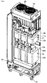
- Fig. 2 is a perspective view showing the exterior of the filter device shown in Fig. 1 .
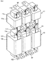
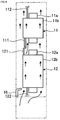
- Figs. 3 and 4 are each a perspective view showing the internal structure of the filter device.
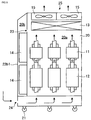
- Fig. 5 is a schematic diagram schematically showing a configuration of the filter device.
- the filter main body 20 can be moved on wheels 21 attached to the lower end portion of the filter main body 20, and has two separate chambers 22a, 22b.
- the filter reactors 11, booster reactors 12, and filter resistor members 13 are disposed in the chamber 22a (also referred to as “rear chamber 22a,” hereinafter), while the filter capacitors 14 are disposed in the chamber 22b (also referred to as "front chamber 22b,” hereinafter).
- These two chambers 22a, 22b communicate with each other by an upper opening 23.
- the filter main body 20 is also provided with an inlet 24 and an outlet 25.
- the inlet 24 is formed in the lower portion of a front cover 22b1 that closes the front chamber 22b in which the filter capacitors 14 are disposed, and communicates with the rear chamber 22a in which the filter reactors 11 and the like are disposed.
- the outlet 25 is an opening formed in an upper surface of the rear chamber 22a and is configured with cooling fans 15.
- each of the cooling fans 15 When driven in response to a drive command, each of the cooling fans 15 functions as the air blowing means for drawing external air into the filter main body 20 through the inlet 24 and blowing the air, which has passed through the filter main body 20, to the outside through the outlet 25.
- Fig. 6 is a perspective view showing the filter reactors and booster reactors that are shown in Fig. 1 .
- the filter reactors 11 and the booster reactors 12 are disposed, in which those filter reactors and boosting reactors that are electrically connected to each other by a common wiring system are disposed in vertical arrangement. More specifically, support plates 30 and support bars 31 are provided in such a manner that the filter reactors 11 are supported immediately above the booster reactors 12.
- the booster reactors 12 are disposed below the respective filter reactors 11 because the booster reactors 12 are heavier than the filter reactors 11.
- each of the booster reactors 12 configures an air passage 125 for air introduced to the filter main body 20, between the iron core 12a and the coil 12b as well as between the inner circumferential portion and the outer circumferential portion of the coil 12b by wrapping the coil 12b around the iron core 12a, with spacers 123 made of an insulating material being interposed appropriately.
- the guide member 16 formed by appropriately bending a steel plate or an insulating material, guides the air entering the filter main body 20 through the inlet 24 to the air passage 125 as the cooling fans 15 are driven.
- the filter reactors 11 may each configure an air passage (not shown) for the air introduced into the filter main body 20, between the iron core 11a and the coil 11b by wrapping the coil 11b around the iron core 11a, with spacers (not shown) made of an insulating material being interposed appropriately.
- the filter resistor members 13 are disposed above the filter reactors 11 and below the cooling fans 15. The filter resistor members 13 generate the most heat and are therefore disposed at the furthest downstream side of the flow of the air passing through the filter main body 20.
- the filter resistor members 13 are each configured by arranging a plurality of flat members 13a horizontally, in which a pathway 13b through which the air passes through are formed between the flat members 13a, as shown in Fig. 9 .
- One end 131 is electrically connected to each filter reactor 11, and the other end 132 is electrically connected to each filter capacitor 14.
- a wiring system that is electrically connected to the filter capacitor 14 passes through the upper opening 23.
- the filter capacitors 14 are disposed in the front chamber 22b, different from the chamber for storing the filter reactors 11, booster reactors 12, and filter resistor members 13. This is because the filter capacitors 14 generate less heat than the filter reactors 11, booster reactors 12, and filter resistor members 13, and because the filter capacitors 14 need to be unaffected by the heat generated by the filter reactors 11, booster reactors 12, and filter resistor members 13.
- the external air enters the filter main body 20 through the inlet 24, as shown in Fig. 5 .
- the air that enters the filter main body 20 passes through the inside of the filter main body 20 toward the outlet 25 and is guided to the air passage 125 of each booster reactor 12 by the guide member 16 as shown in Fig. 8 to pass through the air passage 125 of each booster reactor 12.
- the air After passing through the air passages 125 of the booster reactors 12, the air passes through the periphery of each filter reactor 11, then passes through the periphery of each filter resistor member 13, and is blown out of the outlet 25 to the outside.
- the booster reactors 12 are cooled by the passage of the air through the air passages 125, and the filter reactors 11 are cooled by the passage of the air through the booster reactors 12.
- the filter resistor members 13 are cooled by the passage of the air through the filter reactors 11.
- each of the booster reactors 12 configures the air passage 125 between the inner circumferential portion and the outer circumferential portion of the coil 12b by wrapping the coil 12b around the iron core 12a, with the spacers 123 being interposed appropriately.
- the booster reactors 12 are stored in the filter device 10 in such a manner that the air that has passed through the air passages 125 passes through the periphery of each of the filter reactors 11 disposed immediately above the booster reactors 12.
- the booster reactors 12 are stored in a vertical arrangement with respect to the filter reactors 11.
- Such a configuration can sufficiently reduce the width of the place where the filter reactors 11 and booster reactors 12 are disposed, as well as the width of the filter main body 20.
- the booster reactors 12 allow the passage of the air through the air passages 125 configured by the booster reactors 12, increasing the area of contact between the air passages and the air and hence the heat dissipation area. Therefore, while reducing the size of the entire device, favorable cooling of the filter reactors 11 and the booster reactors 12 can be realized.
- the filter resistor members 13 are disposed in the region where the air, which has passed through the peripheries of the filter reactors 11, passes through. Therefore, the air that has passed through the filter resistor members 13 generating the most heat does not pass through the peripheries of the filter reactors 11 and the like, achieving favorable cooling of the filter reactors 11 and booster reactors 12.
- the guide member 16 is disposed below the booster reactors 12.
- a guide member for guiding, to the air passages of the filter reactors 11, the air that has passed through the booster reactors 12 may be disposed below the filter reactors 11.
- the cooling fans 15 are disposed above the rear chamber 22a as components of the outlet 25.
- the air blowing means may be disposed anywhere in the casing.
Landscapes
- Engineering & Computer Science (AREA)
- Power Engineering (AREA)
- Inverter Devices (AREA)
- Transformer Cooling (AREA)
- Coils Of Transformers For General Uses (AREA)
- Power Conversion In General (AREA)
Abstract
Description
- The present invention relates to a filter device.
- There has been known a technique for suppressing the high-frequency currents by electrically connecting a filter reactor and a booster reactor between a power supply and a power converter having a converter unit for rectifying the inputs and an inverter unit for inversely converting the outputs of the converter unit. Such filter reactor and booster reactor are typically disposed separately in the vicinity of the place where the power converter is installed.
- For the purpose of reducing the number of installation spaces and the wiring workload, a configuration in which a filter reactor and the like are incorporated in a single module has been proposed (see Patent Literature 1, for example).
- Patent Literature 1: Japanese Patent Application Publication No.
2005-287183 - Although Patent Literature 1 describes that a filter reactor and the like are incorporated in a single module, a specific configuration thereof is not described therein. In addition, when placing the filter reactor and the like within a casing, it is preferred that the casing be small in view of the transport thereof and that the reactor and the like be cooled favorably.
- In view of the forgoing circumstances, an object of the present invention is to provide a filter device that is configured to accomplish size reduction of the entire device and to favorably cool a filter reactor and a booster reactor therein.
- In order to achieve the foregoing object, a filter device according to the present invention is a filter device, which is electrically connected between a power supply and a power converter that includes a converter unit for rectifying inputs and an inverter unit for inversely converting outputs of the converter unit, the filter device being configured such that a filter reactor for removing a high-frequency component and a booster reactor for boosting a voltage of a current having passed through the filter reactor are stored in a casing, wherein the booster reactor configures an air passage for air introduced into the casing, between an inner circumferential portion and an outer circumferential portion of a coil by wrapping the coil around an iron core, with spacers interposed appropriately, and is stored in the casing in such a manner that air that has passed through the air passage passes through a periphery of the filter reactor disposed immediately above the booster reactor.
- The filter device according to the present invention is also characterized in having air blowing means for drawing external air into the casing through an inlet formed in the casing and blowing the air that has passed through the inside of the casing to the outside through an outlet formed in the casing, and a guide member that is disposed inside the casing and guides, to the air passage, the air that is drawn through the inlet.
- The filter device according to the present invention is also characterized in further having a filter resistor member for allowing the passage of a current with a high-frequency component that is removed by the filter reactor, wherein the filter resistor member is disposed in a passage region of the air that has passed through the periphery of the filter reactor.
- The filter device according to the present invention is characterized in further having a filter capacitor for accumulating a current with a high-frequency component that has passed through the filter resistor member, wherein the filter capacitor is disposed in a chamber partitioned from a chamber in which the filter reactor and the booster reactor are stored.
- According to the present invention, the booster reactor configures an air passage for air introduced into the casing, between the inner circumferential portion and the outer circumferential portion of a coil by wrapping the coil around an iron core, with spacers interposed appropriately, and is stored in the casing in such a manner that air that has passed through the air passage passes through the periphery of the filter reactor disposed immediately above the booster reactor. This means that the booster reactor is stored in the casing in a vertical arrangement with respect to the filter reactor. Accordingly, the width of the place where the filter reactor and the booster reactor are installed can be reduced sufficiently, resulting in a reduction of the width of the casing. Moreover, because the booster reactor allows the passage of air to the air passage configured by the booster reactor, the area of contact between the air passage and the air can be expanded, increasing the heat dissipation area. Therefore, while reducing the size of the entire filter device, the effect of favorably cooling the filter reactor and the booster reactor can be realized.
-
-
Fig. 1 is a connection diagram to which a filter device according to an embodiment of the present invention is applied; -
Fig. 2 is a perspective view showing the exterior of the filter device shown inFig. 1 ; -
Fig. 3 is a perspective view showing an internal structure of the filter device; -
Fig. 4 is a perspective view showing the internal structure of the filter device; -
Fig. 5 is a schematic diagram schematically showing a configuration of the filter device; -
Fig. 6 is a perspective view showing filter reactors and booster reactors that are shown inFig. 1 ; -
Fig. 7 is a plan view showing an internal structure of the booster reactor; -
Fig. 8 is a schematic diagram schematically showing the back of the internal structure of a filter main body; and -
Fig. 9 is a plan view showing a configuration of a filter resistor member. - A preferred embodiment of the filter device according to the present invention is described hereinafter in detail with reference to the accompanying drawings.
-
Fig. 1 is a connection diagram to which a filter device according to an embodiment of the present invention is applied. As shown inFig. 1 , afilter device 10 is electrically connected between an AC power supply 1 and apower converter 2. Thepower converter 2 has a converter unit 3 that converts an AC current into a DC current and an inverter unit 4 that converts the DC current output from the converter unit 3 into an AC current to drive a load 5 such as a motor. The converter unit 3 and the inverter unit 4 are stored in separate, dedicated casings. - The
filter device 10 has a filtermain body 20 as a casing for storingfilter reactors 11,booster reactors 12,filter resistor members 13, andfilter capacitors 14. - The
filter reactors 11 remove a specific high-frequency component. Thebooster reactors 12 boost the voltage of a current that has passed through thefilter reactors 11. Thefilter resistor members 13 allow the passage of a current having a high-frequency component that is removed by thefilter reactors 11. Thefilter capacitors 14 accumulate the current having a high-frequency component that has passed through thefilter resistor members 13. -
Fig. 2 is a perspective view showing the exterior of the filter device shown inFig. 1 .Figs. 3 and4 are each a perspective view showing the internal structure of the filter device.Fig. 5 is a schematic diagram schematically showing a configuration of the filter device. - As shown in
Figs. 2 to 5 , the filtermain body 20 can be moved onwheels 21 attached to the lower end portion of the filtermain body 20, and has twoseparate chambers main body 20, thefilter reactors 11,booster reactors 12, andfilter resistor members 13 are disposed in thechamber 22a (also referred to as "rear chamber 22a," hereinafter), while thefilter capacitors 14 are disposed in thechamber 22b (also referred to as "front chamber 22b," hereinafter). These twochambers upper opening 23. - The filter
main body 20 is also provided with aninlet 24 and anoutlet 25. Theinlet 24 is formed in the lower portion of a front cover 22b1 that closes thefront chamber 22b in which thefilter capacitors 14 are disposed, and communicates with therear chamber 22a in which thefilter reactors 11 and the like are disposed. Theoutlet 25 is an opening formed in an upper surface of therear chamber 22a and is configured withcooling fans 15. - When driven in response to a drive command, each of the
cooling fans 15 functions as the air blowing means for drawing external air into the filtermain body 20 through theinlet 24 and blowing the air, which has passed through the filtermain body 20, to the outside through theoutlet 25. -
Fig. 6 is a perspective view showing the filter reactors and booster reactors that are shown inFig. 1 . Thefilter reactors 11 and thebooster reactors 12 are disposed, in which those filter reactors and boosting reactors that are electrically connected to each other by a common wiring system are disposed in vertical arrangement. More specifically,support plates 30 andsupport bars 31 are provided in such a manner that thefilter reactors 11 are supported immediately above thebooster reactors 12. Here, thebooster reactors 12 are disposed below therespective filter reactors 11 because thebooster reactors 12 are heavier than thefilter reactors 11. - The
filter reactors 11 and thebooster reactors 12 are each configured by wrapping acoil iron core conductor bar 111 provided at one end of thecoil 11b of thecorresponding filter reactor 11 is coupled to aconductor bar 121 provided at one end of thecoil 12b of thecorresponding booster reactor 12, thereby electrically connecting thefilter reactor 11 to thebooster reactor 12. Aconductor bar 112 is brazed to the other end of thecoil 11b of thecorresponding filter reactor 11, and is electrically connected to the correspondingfilter resistor member 13. Aconductor bar 122 is brazed to the other end of thecoil 12b of thecorresponding booster reactor 12, and is electrically connected to the converter unit 3 of thepower converter 2 by an output terminal, not shown. - Incidentally, the
booster reactors 12 are designed as follows. Specifically, as shown inFig. 7 , each of thebooster reactors 12 configures anair passage 125 for air introduced to the filtermain body 20, between theiron core 12a and thecoil 12b as well as between the inner circumferential portion and the outer circumferential portion of thecoil 12b by wrapping thecoil 12b around theiron core 12a, withspacers 123 made of an insulating material being interposed appropriately. - Below the
booster reactors 12 is aguide member 16. Theguide member 16, formed by appropriately bending a steel plate or an insulating material, guides the air entering the filtermain body 20 through theinlet 24 to theair passage 125 as thecooling fans 15 are driven. - As with the
booster reactors 12, thefilter reactors 11 may each configure an air passage (not shown) for the air introduced into the filtermain body 20, between theiron core 11a and thecoil 11b by wrapping thecoil 11b around theiron core 11a, with spacers (not shown) made of an insulating material being interposed appropriately. - The
filter resistor members 13 are disposed above thefilter reactors 11 and below thecooling fans 15. Thefilter resistor members 13 generate the most heat and are therefore disposed at the furthest downstream side of the flow of the air passing through the filtermain body 20. Thefilter resistor members 13 are each configured by arranging a plurality offlat members 13a horizontally, in which apathway 13b through which the air passes through are formed between theflat members 13a, as shown inFig. 9 . Oneend 131 is electrically connected to eachfilter reactor 11, and theother end 132 is electrically connected to eachfilter capacitor 14. A wiring system that is electrically connected to thefilter capacitor 14 passes through theupper opening 23. - The
filter capacitors 14 are disposed in thefront chamber 22b, different from the chamber for storing thefilter reactors 11,booster reactors 12, and filterresistor members 13. This is because thefilter capacitors 14 generate less heat than thefilter reactors 11,booster reactors 12, and filterresistor members 13, and because thefilter capacitors 14 need to be unaffected by the heat generated by thefilter reactors 11,booster reactors 12, and filterresistor members 13. - In the
filter device 10 having the foregoing configuration, when the coolingfans 15 are driven, the external air enters the filtermain body 20 through theinlet 24, as shown inFig. 5 . The air that enters the filtermain body 20 passes through the inside of the filtermain body 20 toward theoutlet 25 and is guided to theair passage 125 of eachbooster reactor 12 by theguide member 16 as shown inFig. 8 to pass through theair passage 125 of eachbooster reactor 12. After passing through theair passages 125 of thebooster reactors 12, the air passes through the periphery of eachfilter reactor 11, then passes through the periphery of eachfilter resistor member 13, and is blown out of theoutlet 25 to the outside. - The
booster reactors 12 are cooled by the passage of the air through theair passages 125, and thefilter reactors 11 are cooled by the passage of the air through thebooster reactors 12. Thefilter resistor members 13 are cooled by the passage of the air through thefilter reactors 11. - Incidentally, in the
front chamber 22b in which thefilter capacitors 14 are disposed, driving the coolingfans 15 draws the internal air into the coolingfans 15 through theupper opening 23 and blows the air to the outside. As a result, thefilter capacitors 14 that generate less heat than thebooster reactors 12 and the like are also cooled by the passage of the air therethrough. - According to the
filter device 10 of the embodiment of the present invention described above, each of thebooster reactors 12 configures theair passage 125 between the inner circumferential portion and the outer circumferential portion of thecoil 12b by wrapping thecoil 12b around theiron core 12a, with thespacers 123 being interposed appropriately. Thebooster reactors 12 are stored in thefilter device 10 in such a manner that the air that has passed through theair passages 125 passes through the periphery of each of thefilter reactors 11 disposed immediately above thebooster reactors 12. In other words, thebooster reactors 12 are stored in a vertical arrangement with respect to thefilter reactors 11. Such a configuration can sufficiently reduce the width of the place where thefilter reactors 11 andbooster reactors 12 are disposed, as well as the width of the filtermain body 20. Moreover, thebooster reactors 12 allow the passage of the air through theair passages 125 configured by thebooster reactors 12, increasing the area of contact between the air passages and the air and hence the heat dissipation area. Therefore, while reducing the size of the entire device, favorable cooling of thefilter reactors 11 and thebooster reactors 12 can be realized. - According to the
filter device 10, when the coolingfans 15 are driven, the coolingfans 15 draw the external air into the filtermain body 20 through theinlet 24 and blow the air, which has passed through the inside of the filtermain body 20, to the outside through theoutlet 25, in which theguide member 16 disposed in the filtermain body 20 guides the air drawn through theinlet 24 to theair passages 125. Therefore, the air that is drawn from the outside can be guided to theair passages 125 efficiently. In addition, the efficiency of cooling thefilter reactors 11 and thebooster reactors 12 can be improved by increasing the amount of air passing through theair passages 125. - According to the
filter device 10, thefilter resistor members 13 are disposed in the region where the air, which has passed through the peripheries of thefilter reactors 11, passes through. Therefore, the air that has passed through thefilter resistor members 13 generating the most heat does not pass through the peripheries of thefilter reactors 11 and the like, achieving favorable cooling of thefilter reactors 11 andbooster reactors 12. - According to the
filter device 10, thefilter capacitors 14 are disposed in thefront chamber 22b that is partitioned from therear chamber 22a for storing thefilter reactors 11 and thebooster reactors 12. This configuration can prevent thefilter capacitors 14 from being affected negatively by the heat generated by the heat generating elements of thefilter reactors 11 and the like. - A preferred embodiment of the present invention was described above. However, the present invention is not limited thereto, and various changes can be made to the present invention.
- According to the foregoing embodiment, the
guide member 16 is disposed below thebooster reactors 12. In the present invention, however, a guide member for guiding, to the air passages of thefilter reactors 11, the air that has passed through thebooster reactors 12 may be disposed below thefilter reactors 11. - According to the foregoing embodiment, the cooling
fans 15 are disposed above therear chamber 22a as components of theoutlet 25. In the present invention, however, the air blowing means may be disposed anywhere in the casing. -
- 1
- AC power supply
- 2
- Power converter
- 3
- Converter unit
- 4
- Inverter unit
- 10
- Filter device
- 11
- Filter reactor
- 11 a
- Iron core
- 11b
- Coil
- 12
- Booster reactor
- 12a
- Iron core
- 12b
- Coil
- 123
- Spacer
- 125
- Air passage
- 13
- Filter resistor member
- 14
- Filter capacitor
- 15
- Cooling fan
- 16
- Guide member
- 20
- Filter main body
- 21
- Wheel
- 22a
- Rear chamber
- 22b
- Front chamber
- 23
- Upper opening
- 24
- Inlet
- 25
- Outlet
Claims (5)
- A filter device, which is electrically connected between a power supply and a power converter that includes a converter unit for rectifying inputs and an inverter unit for inversely converting outputs of the converter unit, the filter device being configured such that a filter reactor for removing a high-frequency component and a booster reactor for boosting a voltage of a current having passed through the filter reactor are stored in a casing,
wherein the booster reactor configures an air passage for air introduced into the casing, between an inner circumferential portion and an outer circumferential portion of a coil by wrapping the coil around an iron core, with spacers interposed appropriately, and is stored in the casing in such a manner that air that has passed through the air passage passes through a periphery of the filter reactor disposed immediately above the booster reactor. - The filter device, comprising:air blowing means for drawing external air into the casing through an inlet formed in the casing and blowing the air that has passed through the inside of the casing to the outside through an outlet formed in the casing; anda guide member that is disposed inside the casing and guides, to the air passage, the air that is drawn through the inlet.
- The filter device according to claim 1, further comprising a filter resistor member for allowing the passage of a current with a high-frequency component that is removed by the filter reactor,
wherein the filter resistor member is disposed in a passage region of the air that has passed through the periphery of the filter reactor. - The filter device according to claim 2, further comprising a filter resistor member for allowing the passage of a current with a high-frequency component that is removed by the filter reactor,
wherein the filter resistor member is disposed in a passage region of the air that has passed through the periphery of the filter reactor. - The filter device according to any one of claims 1 to 4, further comprising a filter capacitor for accumulating a current with a high-frequency component that has passed through the filter resistor member,
wherein the filter capacitor is disposed in a chamber partitioned from a chamber in which the filter reactor and the booster reactor are stored.
Applications Claiming Priority (2)
| Application Number | Priority Date | Filing Date | Title |
|---|---|---|---|
| JP2013185255 | 2013-09-06 | ||
| PCT/JP2014/070120 WO2015033710A1 (en) | 2013-09-06 | 2014-07-30 | Filter device |
Publications (3)
| Publication Number | Publication Date |
|---|---|
| EP3043462A1 true EP3043462A1 (en) | 2016-07-13 |
| EP3043462A4 EP3043462A4 (en) | 2017-07-12 |
| EP3043462B1 EP3043462B1 (en) | 2020-04-22 |
Family
ID=52628195
Family Applications (1)
| Application Number | Title | Priority Date | Filing Date |
|---|---|---|---|
| EP14842865.9A Active EP3043462B1 (en) | 2013-09-06 | 2014-07-30 | Filter device |
Country Status (5)
| Country | Link |
|---|---|
| US (1) | US9691535B2 (en) |
| EP (1) | EP3043462B1 (en) |
| JP (1) | JP6086156B2 (en) |
| CN (1) | CN105027410B (en) |
| WO (1) | WO2015033710A1 (en) |
Families Citing this family (13)
| Publication number | Priority date | Publication date | Assignee | Title |
|---|---|---|---|---|
| US9241430B2 (en) * | 2013-03-15 | 2016-01-19 | Eaton Corporation | Power pole isolated heat pipe inverter assembly |
| JP6382657B2 (en) * | 2014-09-18 | 2018-08-29 | 株式会社東芝 | Power converter |
| JP6693177B2 (en) * | 2016-03-03 | 2020-05-13 | 富士電機株式会社 | Filter unit for converter |
| DE202016102587U1 (en) * | 2016-05-13 | 2016-06-10 | Schaffner Emv Ag | filter |
| KR102257074B1 (en) * | 2016-12-26 | 2021-05-27 | 미쓰비시덴키 가부시키가이샤 | Filter device and power conversion device |
| TWM541152U (en) * | 2017-01-12 | 2017-05-01 | Chyng Hong Electronic Co Ltd | Choke module for high power density DC to DC power converter |
| US10374421B2 (en) | 2017-03-24 | 2019-08-06 | Abb Schweiz Ag | Systems and methods for line voltage drop compensation |
| JP6692499B2 (en) * | 2017-07-21 | 2020-05-13 | 三菱電機株式会社 | Station building power supply |
| EP3701604B1 (en) * | 2017-10-23 | 2024-04-03 | Eaton Intelligent Power Limited | Electrical cabinet with vortex-entrained airflow |
| DE102017126599A1 (en) * | 2017-11-13 | 2019-05-16 | Schmidbauer Transformatoren und Gerätebau GmbH | inductance |
| JP2021119584A (en) * | 2020-01-30 | 2021-08-12 | 株式会社明電舎 | Cooling structure of board |
| JP7312332B2 (en) * | 2020-08-24 | 2023-07-20 | 日立三菱水力株式会社 | Modular multilevel power converters and modular multilevel power conversion systems |
| JP7291433B1 (en) | 2022-03-02 | 2023-06-15 | 株式会社左尾電機 | Reactor mounting structure |
Family Cites Families (12)
| Publication number | Priority date | Publication date | Assignee | Title |
|---|---|---|---|---|
| JPS574216U (en) * | 1980-06-09 | 1982-01-09 | ||
| JPS5744521U (en) * | 1980-08-26 | 1982-03-11 | ||
| JPH0888490A (en) * | 1994-09-20 | 1996-04-02 | Hitachi Ltd | Cooling device for vehicle control device |
| DE29800567U1 (en) * | 1998-01-14 | 1998-04-09 | Siemens AG, 80333 München | Damping filter arrangement for converters with regulated voltage intermediate circuit and sinusoidal phase currents |
| JP2005287183A (en) * | 2004-03-30 | 2005-10-13 | Yaskawa Electric Corp | Semiconductor power converter |
| US7746020B2 (en) * | 2007-01-22 | 2010-06-29 | Johnson Controls Technology Company | Common mode & differential mode filter for variable speed drive |
| JP5025405B2 (en) * | 2007-09-28 | 2012-09-12 | 株式会社東芝 | Cooling system for railway vehicles |
| US8575479B2 (en) * | 2009-06-30 | 2013-11-05 | TECO—Westinghouse Motor Company | Providing a transformer for an inverter |
| US8325500B2 (en) * | 2010-07-13 | 2012-12-04 | Eaton Corporation | Inverter filter including differential mode and common mode, and system including the same |
| JP5483209B2 (en) * | 2011-03-30 | 2014-05-07 | 株式会社安川電機 | Power converter |
| US9318253B2 (en) * | 2014-05-02 | 2016-04-19 | Hamilton Sundstrand Corporation | Hybrid planar common-mode choke |
| JP5877875B2 (en) * | 2014-05-30 | 2016-03-08 | ファナック株式会社 | LC filter with a function to cool the AC reactor |
-
2014
- 2014-07-30 WO PCT/JP2014/070120 patent/WO2015033710A1/en not_active Ceased
- 2014-07-30 JP JP2015535385A patent/JP6086156B2/en active Active
- 2014-07-30 CN CN201480012967.XA patent/CN105027410B/en active Active
- 2014-07-30 EP EP14842865.9A patent/EP3043462B1/en active Active
-
2015
- 2015-09-08 US US14/847,696 patent/US9691535B2/en active Active
Non-Patent Citations (1)
| Title |
|---|
| See references of WO2015033710A1 * |
Also Published As
| Publication number | Publication date |
|---|---|
| JPWO2015033710A1 (en) | 2017-03-02 |
| US9691535B2 (en) | 2017-06-27 |
| EP3043462B1 (en) | 2020-04-22 |
| CN105027410B (en) | 2017-12-22 |
| US20150380147A1 (en) | 2015-12-31 |
| WO2015033710A1 (en) | 2015-03-12 |
| JP6086156B2 (en) | 2017-03-01 |
| CN105027410A (en) | 2015-11-04 |
| EP3043462A4 (en) | 2017-07-12 |
Similar Documents
| Publication | Publication Date | Title |
|---|---|---|
| EP3043462B1 (en) | Filter device | |
| US10629396B2 (en) | Arc flash resistant enclosure with segregated cooling | |
| US10658939B2 (en) | Power conversion apparatus and noise filter | |
| JP5549120B2 (en) | Power conversion device for railway vehicles | |
| US20170238445A1 (en) | Inverter and method for cooling an inverter | |
| CN102398503A (en) | Vehicle with a steering wheel | |
| CN105939117B (en) | Power conversion device | |
| KR20140117634A (en) | Main circuit system for electric rolling stock | |
| JP5382874B2 (en) | Power control unit | |
| JP7015642B2 (en) | filter | |
| KR101655515B1 (en) | Power converting apparatus for vehicle | |
| CN102791090A (en) | Automotive electrical box module | |
| EP2672618A1 (en) | Modular motor inverter arrangement with cooling sections forming inner duct ring capacitor on the outside | |
| CN104868702A (en) | Converter power cabinet | |
| CN111884527A (en) | Power conversion device | |
| CN204316303U (en) | A kind of current transformer power cabinet | |
| US20150351278A1 (en) | Lc filter having a function to cool ac reactor | |
| JP2010200433A (en) | Power converter | |
| CN206099764U (en) | Double - circuit BUCK power structure | |
| JP2013074722A (en) | Power conversion device | |
| CN105450043A (en) | Traction inversion module and traction inverter | |
| JP6458529B2 (en) | Power converter | |
| JP2013085399A (en) | Quick charger | |
| JP2016220343A (en) | Power conversion device | |
| JP2009056816A (en) | Electric car |
Legal Events
| Date | Code | Title | Description |
|---|---|---|---|
| PUAI | Public reference made under article 153(3) epc to a published international application that has entered the european phase |
Free format text: ORIGINAL CODE: 0009012 |
|
| 17P | Request for examination filed |
Effective date: 20150828 |
|
| AK | Designated contracting states |
Kind code of ref document: A1 Designated state(s): AL AT BE BG CH CY CZ DE DK EE ES FI FR GB GR HR HU IE IS IT LI LT LU LV MC MK MT NL NO PL PT RO RS SE SI SK SM TR |
|
| AX | Request for extension of the european patent |
Extension state: BA ME |
|
| DAX | Request for extension of the european patent (deleted) | ||
| A4 | Supplementary search report drawn up and despatched |
Effective date: 20170613 |
|
| RIC1 | Information provided on ipc code assigned before grant |
Ipc: H02M 1/12 20060101ALI20170607BHEP Ipc: H03H 7/01 20060101ALI20170607BHEP Ipc: H02M 5/42 20060101ALI20170607BHEP Ipc: H01F 27/28 20060101ALI20170607BHEP Ipc: H02M 7/00 20060101ALI20170607BHEP Ipc: H01F 27/02 20060101ALI20170607BHEP Ipc: H01F 37/00 20060101ALI20170607BHEP Ipc: H02M 7/06 20060101AFI20170607BHEP Ipc: H01F 27/08 20060101ALI20170607BHEP Ipc: H02J 3/01 20060101ALI20170607BHEP |
|
| GRAP | Despatch of communication of intention to grant a patent |
Free format text: ORIGINAL CODE: EPIDOSNIGR1 |
|
| STAA | Information on the status of an ep patent application or granted ep patent |
Free format text: STATUS: GRANT OF PATENT IS INTENDED |
|
| INTG | Intention to grant announced |
Effective date: 20191129 |
|
| GRAS | Grant fee paid |
Free format text: ORIGINAL CODE: EPIDOSNIGR3 |
|
| GRAA | (expected) grant |
Free format text: ORIGINAL CODE: 0009210 |
|
| STAA | Information on the status of an ep patent application or granted ep patent |
Free format text: STATUS: THE PATENT HAS BEEN GRANTED |
|
| AK | Designated contracting states |
Kind code of ref document: B1 Designated state(s): AL AT BE BG CH CY CZ DE DK EE ES FI FR GB GR HR HU IE IS IT LI LT LU LV MC MK MT NL NO PL PT RO RS SE SI SK SM TR |
|
| REG | Reference to a national code |
Ref country code: CH Ref legal event code: EP |
|
| REG | Reference to a national code |
Ref country code: IE Ref legal event code: FG4D |
|
| REG | Reference to a national code |
Ref country code: DE Ref legal event code: R096 Ref document number: 602014064265 Country of ref document: DE |
|
| REG | Reference to a national code |
Ref country code: AT Ref legal event code: REF Ref document number: 1261466 Country of ref document: AT Kind code of ref document: T Effective date: 20200515 |
|
| REG | Reference to a national code |
Ref country code: LT Ref legal event code: MG4D |
|
| REG | Reference to a national code |
Ref country code: NL Ref legal event code: MP Effective date: 20200422 |
|
| PG25 | Lapsed in a contracting state [announced via postgrant information from national office to epo] |
Ref country code: LT Free format text: LAPSE BECAUSE OF FAILURE TO SUBMIT A TRANSLATION OF THE DESCRIPTION OR TO PAY THE FEE WITHIN THE PRESCRIBED TIME-LIMIT Effective date: 20200422 Ref country code: PT Free format text: LAPSE BECAUSE OF FAILURE TO SUBMIT A TRANSLATION OF THE DESCRIPTION OR TO PAY THE FEE WITHIN THE PRESCRIBED TIME-LIMIT Effective date: 20200824 Ref country code: NL Free format text: LAPSE BECAUSE OF FAILURE TO SUBMIT A TRANSLATION OF THE DESCRIPTION OR TO PAY THE FEE WITHIN THE PRESCRIBED TIME-LIMIT Effective date: 20200422 Ref country code: FI Free format text: LAPSE BECAUSE OF FAILURE TO SUBMIT A TRANSLATION OF THE DESCRIPTION OR TO PAY THE FEE WITHIN THE PRESCRIBED TIME-LIMIT Effective date: 20200422 Ref country code: NO Free format text: LAPSE BECAUSE OF FAILURE TO SUBMIT A TRANSLATION OF THE DESCRIPTION OR TO PAY THE FEE WITHIN THE PRESCRIBED TIME-LIMIT Effective date: 20200722 Ref country code: GR Free format text: LAPSE BECAUSE OF FAILURE TO SUBMIT A TRANSLATION OF THE DESCRIPTION OR TO PAY THE FEE WITHIN THE PRESCRIBED TIME-LIMIT Effective date: 20200723 Ref country code: SE Free format text: LAPSE BECAUSE OF FAILURE TO SUBMIT A TRANSLATION OF THE DESCRIPTION OR TO PAY THE FEE WITHIN THE PRESCRIBED TIME-LIMIT Effective date: 20200422 Ref country code: IS Free format text: LAPSE BECAUSE OF FAILURE TO SUBMIT A TRANSLATION OF THE DESCRIPTION OR TO PAY THE FEE WITHIN THE PRESCRIBED TIME-LIMIT Effective date: 20200822 |
|
| REG | Reference to a national code |
Ref country code: AT Ref legal event code: MK05 Ref document number: 1261466 Country of ref document: AT Kind code of ref document: T Effective date: 20200422 |
|
| PG25 | Lapsed in a contracting state [announced via postgrant information from national office to epo] |
Ref country code: LV Free format text: LAPSE BECAUSE OF FAILURE TO SUBMIT A TRANSLATION OF THE DESCRIPTION OR TO PAY THE FEE WITHIN THE PRESCRIBED TIME-LIMIT Effective date: 20200422 Ref country code: RS Free format text: LAPSE BECAUSE OF FAILURE TO SUBMIT A TRANSLATION OF THE DESCRIPTION OR TO PAY THE FEE WITHIN THE PRESCRIBED TIME-LIMIT Effective date: 20200422 Ref country code: HR Free format text: LAPSE BECAUSE OF FAILURE TO SUBMIT A TRANSLATION OF THE DESCRIPTION OR TO PAY THE FEE WITHIN THE PRESCRIBED TIME-LIMIT Effective date: 20200422 Ref country code: BG Free format text: LAPSE BECAUSE OF FAILURE TO SUBMIT A TRANSLATION OF THE DESCRIPTION OR TO PAY THE FEE WITHIN THE PRESCRIBED TIME-LIMIT Effective date: 20200722 |
|
| PG25 | Lapsed in a contracting state [announced via postgrant information from national office to epo] |
Ref country code: AL Free format text: LAPSE BECAUSE OF FAILURE TO SUBMIT A TRANSLATION OF THE DESCRIPTION OR TO PAY THE FEE WITHIN THE PRESCRIBED TIME-LIMIT Effective date: 20200422 |
|
| REG | Reference to a national code |
Ref country code: DE Ref legal event code: R097 Ref document number: 602014064265 Country of ref document: DE |
|
| PG25 | Lapsed in a contracting state [announced via postgrant information from national office to epo] |
Ref country code: IT Free format text: LAPSE BECAUSE OF FAILURE TO SUBMIT A TRANSLATION OF THE DESCRIPTION OR TO PAY THE FEE WITHIN THE PRESCRIBED TIME-LIMIT Effective date: 20200422 Ref country code: ES Free format text: LAPSE BECAUSE OF FAILURE TO SUBMIT A TRANSLATION OF THE DESCRIPTION OR TO PAY THE FEE WITHIN THE PRESCRIBED TIME-LIMIT Effective date: 20200422 Ref country code: RO Free format text: LAPSE BECAUSE OF FAILURE TO SUBMIT A TRANSLATION OF THE DESCRIPTION OR TO PAY THE FEE WITHIN THE PRESCRIBED TIME-LIMIT Effective date: 20200422 Ref country code: CZ Free format text: LAPSE BECAUSE OF FAILURE TO SUBMIT A TRANSLATION OF THE DESCRIPTION OR TO PAY THE FEE WITHIN THE PRESCRIBED TIME-LIMIT Effective date: 20200422 Ref country code: DK Free format text: LAPSE BECAUSE OF FAILURE TO SUBMIT A TRANSLATION OF THE DESCRIPTION OR TO PAY THE FEE WITHIN THE PRESCRIBED TIME-LIMIT Effective date: 20200422 Ref country code: SM Free format text: LAPSE BECAUSE OF FAILURE TO SUBMIT A TRANSLATION OF THE DESCRIPTION OR TO PAY THE FEE WITHIN THE PRESCRIBED TIME-LIMIT Effective date: 20200422 Ref country code: EE Free format text: LAPSE BECAUSE OF FAILURE TO SUBMIT A TRANSLATION OF THE DESCRIPTION OR TO PAY THE FEE WITHIN THE PRESCRIBED TIME-LIMIT Effective date: 20200422 Ref country code: AT Free format text: LAPSE BECAUSE OF FAILURE TO SUBMIT A TRANSLATION OF THE DESCRIPTION OR TO PAY THE FEE WITHIN THE PRESCRIBED TIME-LIMIT Effective date: 20200422 |
|
| REG | Reference to a national code |
Ref country code: DE Ref legal event code: R119 Ref document number: 602014064265 Country of ref document: DE |
|
| PG25 | Lapsed in a contracting state [announced via postgrant information from national office to epo] |
Ref country code: SK Free format text: LAPSE BECAUSE OF FAILURE TO SUBMIT A TRANSLATION OF THE DESCRIPTION OR TO PAY THE FEE WITHIN THE PRESCRIBED TIME-LIMIT Effective date: 20200422 Ref country code: MC Free format text: LAPSE BECAUSE OF FAILURE TO SUBMIT A TRANSLATION OF THE DESCRIPTION OR TO PAY THE FEE WITHIN THE PRESCRIBED TIME-LIMIT Effective date: 20200422 Ref country code: PL Free format text: LAPSE BECAUSE OF FAILURE TO SUBMIT A TRANSLATION OF THE DESCRIPTION OR TO PAY THE FEE WITHIN THE PRESCRIBED TIME-LIMIT Effective date: 20200422 |
|
| PLBE | No opposition filed within time limit |
Free format text: ORIGINAL CODE: 0009261 |
|
| REG | Reference to a national code |
Ref country code: CH Ref legal event code: PL |
|
| STAA | Information on the status of an ep patent application or granted ep patent |
Free format text: STATUS: NO OPPOSITION FILED WITHIN TIME LIMIT |
|
| 26N | No opposition filed |
Effective date: 20210125 |
|
| GBPC | Gb: european patent ceased through non-payment of renewal fee |
Effective date: 20200730 |
|
| REG | Reference to a national code |
Ref country code: BE Ref legal event code: MM Effective date: 20200731 |
|
| PG25 | Lapsed in a contracting state [announced via postgrant information from national office to epo] |
Ref country code: LU Free format text: LAPSE BECAUSE OF NON-PAYMENT OF DUE FEES Effective date: 20200730 Ref country code: LI Free format text: LAPSE BECAUSE OF NON-PAYMENT OF DUE FEES Effective date: 20200731 Ref country code: GB Free format text: LAPSE BECAUSE OF NON-PAYMENT OF DUE FEES Effective date: 20200730 Ref country code: CH Free format text: LAPSE BECAUSE OF NON-PAYMENT OF DUE FEES Effective date: 20200731 |
|
| PG25 | Lapsed in a contracting state [announced via postgrant information from national office to epo] |
Ref country code: DE Free format text: LAPSE BECAUSE OF NON-PAYMENT OF DUE FEES Effective date: 20210202 Ref country code: BE Free format text: LAPSE BECAUSE OF NON-PAYMENT OF DUE FEES Effective date: 20200731 Ref country code: SI Free format text: LAPSE BECAUSE OF FAILURE TO SUBMIT A TRANSLATION OF THE DESCRIPTION OR TO PAY THE FEE WITHIN THE PRESCRIBED TIME-LIMIT Effective date: 20200422 |
|
| PG25 | Lapsed in a contracting state [announced via postgrant information from national office to epo] |
Ref country code: IE Free format text: LAPSE BECAUSE OF NON-PAYMENT OF DUE FEES Effective date: 20200730 |
|
| PG25 | Lapsed in a contracting state [announced via postgrant information from national office to epo] |
Ref country code: TR Free format text: LAPSE BECAUSE OF FAILURE TO SUBMIT A TRANSLATION OF THE DESCRIPTION OR TO PAY THE FEE WITHIN THE PRESCRIBED TIME-LIMIT Effective date: 20200422 Ref country code: MT Free format text: LAPSE BECAUSE OF FAILURE TO SUBMIT A TRANSLATION OF THE DESCRIPTION OR TO PAY THE FEE WITHIN THE PRESCRIBED TIME-LIMIT Effective date: 20200422 Ref country code: CY Free format text: LAPSE BECAUSE OF FAILURE TO SUBMIT A TRANSLATION OF THE DESCRIPTION OR TO PAY THE FEE WITHIN THE PRESCRIBED TIME-LIMIT Effective date: 20200422 |
|
| PG25 | Lapsed in a contracting state [announced via postgrant information from national office to epo] |
Ref country code: MK Free format text: LAPSE BECAUSE OF FAILURE TO SUBMIT A TRANSLATION OF THE DESCRIPTION OR TO PAY THE FEE WITHIN THE PRESCRIBED TIME-LIMIT Effective date: 20200422 |
|
| PGFP | Annual fee paid to national office [announced via postgrant information from national office to epo] |
Ref country code: FR Payment date: 20250610 Year of fee payment: 12 |