EP3043376A1 - Silicon carbide semiconductor element and method for manufacturing silicon carbide semiconductor element - Google Patents
Silicon carbide semiconductor element and method for manufacturing silicon carbide semiconductor element Download PDFInfo
- Publication number
- EP3043376A1 EP3043376A1 EP14842165.4A EP14842165A EP3043376A1 EP 3043376 A1 EP3043376 A1 EP 3043376A1 EP 14842165 A EP14842165 A EP 14842165A EP 3043376 A1 EP3043376 A1 EP 3043376A1
- Authority
- EP
- European Patent Office
- Prior art keywords
- silicon carbide
- film
- carbide semiconductor
- infrared ray
- ray absorbing
- Prior art date
- Legal status (The legal status is an assumption and is not a legal conclusion. Google has not performed a legal analysis and makes no representation as to the accuracy of the status listed.)
- Granted
Links
Images




Classifications
-
- H—ELECTRICITY
- H10—SEMICONDUCTOR DEVICES; ELECTRIC SOLID-STATE DEVICES NOT OTHERWISE PROVIDED FOR
- H10D—INORGANIC ELECTRIC SEMICONDUCTOR DEVICES
- H10D12/00—Bipolar devices controlled by the field effect, e.g. insulated-gate bipolar transistors [IGBT]
- H10D12/01—Manufacture or treatment
- H10D12/031—Manufacture or treatment of IGBTs
-
- H—ELECTRICITY
- H10—SEMICONDUCTOR DEVICES; ELECTRIC SOLID-STATE DEVICES NOT OTHERWISE PROVIDED FOR
- H10D—INORGANIC ELECTRIC SEMICONDUCTOR DEVICES
- H10D30/00—Field-effect transistors [FET]
- H10D30/01—Manufacture or treatment
- H10D30/021—Manufacture or treatment of FETs having insulated gates [IGFET]
-
- H—ELECTRICITY
- H10—SEMICONDUCTOR DEVICES; ELECTRIC SOLID-STATE DEVICES NOT OTHERWISE PROVIDED FOR
- H10D—INORGANIC ELECTRIC SEMICONDUCTOR DEVICES
- H10D30/00—Field-effect transistors [FET]
- H10D30/01—Manufacture or treatment
- H10D30/021—Manufacture or treatment of FETs having insulated gates [IGFET]
- H10D30/028—Manufacture or treatment of FETs having insulated gates [IGFET] of double-diffused metal oxide semiconductor [DMOS] FETs
- H10D30/0291—Manufacture or treatment of FETs having insulated gates [IGFET] of double-diffused metal oxide semiconductor [DMOS] FETs of vertical DMOS [VDMOS] FETs
-
- H—ELECTRICITY
- H10—SEMICONDUCTOR DEVICES; ELECTRIC SOLID-STATE DEVICES NOT OTHERWISE PROVIDED FOR
- H10D—INORGANIC ELECTRIC SEMICONDUCTOR DEVICES
- H10D30/00—Field-effect transistors [FET]
- H10D30/60—Insulated-gate field-effect transistors [IGFET]
- H10D30/64—Double-diffused metal-oxide semiconductor [DMOS] FETs
- H10D30/66—Vertical DMOS [VDMOS] FETs
-
- H—ELECTRICITY
- H10—SEMICONDUCTOR DEVICES; ELECTRIC SOLID-STATE DEVICES NOT OTHERWISE PROVIDED FOR
- H10D—INORGANIC ELECTRIC SEMICONDUCTOR DEVICES
- H10D62/00—Semiconductor bodies, or regions thereof, of devices having potential barriers
- H10D62/80—Semiconductor bodies, or regions thereof, of devices having potential barriers characterised by the materials
- H10D62/83—Semiconductor bodies, or regions thereof, of devices having potential barriers characterised by the materials being Group IV materials, e.g. B-doped Si or undoped Ge
- H10D62/832—Semiconductor bodies, or regions thereof, of devices having potential barriers characterised by the materials being Group IV materials, e.g. B-doped Si or undoped Ge being Group IV materials comprising two or more elements, e.g. SiGe
- H10D62/8325—Silicon carbide
-
- H—ELECTRICITY
- H10—SEMICONDUCTOR DEVICES; ELECTRIC SOLID-STATE DEVICES NOT OTHERWISE PROVIDED FOR
- H10D—INORGANIC ELECTRIC SEMICONDUCTOR DEVICES
- H10D64/00—Electrodes of devices having potential barriers
- H10D64/01—Manufacture or treatment
- H10D64/011—Manufacture or treatment of electrodes ohmically coupled to a semiconductor
- H10D64/0111—Manufacture or treatment of electrodes ohmically coupled to a semiconductor to Group IV semiconductors
- H10D64/0115—Manufacture or treatment of electrodes ohmically coupled to a semiconductor to Group IV semiconductors to silicon carbide
-
- H—ELECTRICITY
- H10—SEMICONDUCTOR DEVICES; ELECTRIC SOLID-STATE DEVICES NOT OTHERWISE PROVIDED FOR
- H10D—INORGANIC ELECTRIC SEMICONDUCTOR DEVICES
- H10D64/00—Electrodes of devices having potential barriers
- H10D64/60—Electrodes characterised by their materials
- H10D64/62—Electrodes ohmically coupled to a semiconductor
-
- H—ELECTRICITY
- H10—SEMICONDUCTOR DEVICES; ELECTRIC SOLID-STATE DEVICES NOT OTHERWISE PROVIDED FOR
- H10P—GENERIC PROCESSES OR APPARATUS FOR THE MANUFACTURE OR TREATMENT OF DEVICES COVERED BY CLASS H10
- H10P14/00—Formation of materials, e.g. in the shape of layers or pillars
- H10P14/40—Formation of materials, e.g. in the shape of layers or pillars of conductive or resistive materials
-
- H—ELECTRICITY
- H10—SEMICONDUCTOR DEVICES; ELECTRIC SOLID-STATE DEVICES NOT OTHERWISE PROVIDED FOR
- H10P—GENERIC PROCESSES OR APPARATUS FOR THE MANUFACTURE OR TREATMENT OF DEVICES COVERED BY CLASS H10
- H10P95/00—Generic processes or apparatus for manufacture or treatments not covered by the other groups of this subclass
- H10P95/90—Thermal treatments, e.g. annealing or sintering
Definitions
- the present invention relates to a silicon carbide semiconductor device that uses silicon carbide (SiC) as a semiconductor material and in particular, causes electric current to flow from a front face of a semiconductor substrate to a back face thereof, and a method of manufacturing a silicon carbide semiconductor device.
- SiC silicon carbide
- a silicon carbide semiconductor has a wider band gap compared to that of a silicon (Si) semiconductor and has therefore high breakdown electric field strength.
- "On-resistivity" which is resistivity in the conduction state, is inversely proportional to the cube of the breakdown electric field strength and therefore, in silicon carbide semiconductors (a four-layer-cycle hexagonal crystal: 4H-SiC) that are widely used and called 4-H types, the on-resistivity can be suppressed to be several-hundredths of that of a silicon semiconductor.
- silicon carbide semiconductor With its property of high thermal conductivity that facilitates heat dissipation in addition to the above, the silicon carbide semiconductor is therefore expected to become a next-generation low-loss power semiconductor device.
- Silicon carbide semiconductor devices having various structures have been developed using the silicon carbide semiconductor such as, for example, a Schottky barrier diode, a MOSFET (an insulated gate field-effect transistor), a PN diode, an IGBT (an insulated gate bipolar transistor), and a GTO (a gate turnoff thyristor).
- Non-Patent Literature 1 Ito, Kazuhiro, et al, "Simultaneous Formation of Ni/Al Ohmic Contacts to Both n-and p-Type 4H-SiC", Journal of ELECTRONIC MATERIALS, Vol. 37, No. 11, 2008, pp. 1674-1680
- An ohmic electrode is generally formed by forming a metal film on a silicon carbide semiconductor layer and thereafter, performing annealing under reduced pressure or in an inert gas atmosphere to produce a metal silicide.
- the annealing is generally performed at about 1000 degrees C.
- an alloy is produced between the metals without the formation of metal silicide between the silicon carbide semiconductor layer and the metal. A problem therefore arises in that this does not function as an ohmic electrode.
- a rapid annealing (RTA: Rapid Thermal Annealing) method is a method of efficiently producing a metal silicide.
- the RTA method is based on a mechanism that uses an infrared ray lamp to heat the substrate by a high heating rate, where the object to be heated is generally placed on a carbon susceptor because this annealing also efficiently heats materials having low infrared ray emissivity such as, for example, metal and synthetic quartz materials.
- This uneven formation of the metal silicide causes variance in the contact resistivity and variance in the properties and the reliability of the device.
- one object of the present invention is to enable uniform formation of metal silicide, while minimizing the difference in the contact resistivity between the n-type region and the p-type region and obtaining long-term operating reliability.
- a method of manufacturing a silicon carbide semiconductor device is characterized in that the method includes selectively forming an infrared ray absorbing film on a surface of a silicon carbide semiconductor substrate; sequentially forming on the silicon carbide semiconductor substrate, an aluminum film and a nickel film in an area excluding an area in which the infrared ray absorbing film is formed; and uniformly forming an electrode by a rapid annealing process with a predetermined heating rate on the silicon carbide semiconductor substrate.
- the method is further characterized in that at the rapid annealing process, the silicon carbide semiconductor substrate is placed on a carbon susceptor and heating is performed at an increasing temperature of at least 1 degree C per second with respect to a temperature measurement of the carbon susceptor.
- the method is characterized in that the method further includes roughening a surface of the infrared ray absorbing film.
- a silicon carbide semiconductor device is characterized in that the silicon carbide semiconductor device includes an infrared ray absorbing film selectively formed on a surface of a silicon carbide semiconductor substrate; an aluminum film and a nickel film sequentially formed on the silicon carbide semiconductor substrate, in an area excluding an area in which the infrared ray absorbing film is formed; and an electrode uniformly formed on the silicon carbide semiconductor substrate, by a rapid annealing process with a predetermined heating rate.
- the silicon carbide semiconductor device is further characterized in that the infrared ray absorbing film is formed by at least one of titanium nitride, molybdenum nitride, tungsten nitride, chromium nitride, and a multi-layered film thereof.
- the silicon carbide semiconductor device is characterized in that the infrared ray absorbing film is formed by any one of a multi-layered film of titanium nitride and titanium, a multi-layered film of molybdenum nitride and molybdenum, a multi-layered film of tungsten nitride and tungsten, and a multi-layered film of chromium nitride and chromium.
- the silicon carbide semiconductor device is characterized in that the infrared ray absorbing film is formed having a thickness of at least 10 nm and no more than 300 nm.
- the silicon carbide semiconductor device is characterized in that the aluminum film is formed having a thickness of at least 10 nm and no more than 100 nm.
- the silicon carbide semiconductor device is characterized in that the nickel film is formed having a thickness of at least 20 nm and no more than 100 nm.
- the silicon carbide semiconductor device is characterized in that the infrared ray absorbing film is formed in an active region excluding a source contact electrode portion of a chip area.
- the silicon carbide semiconductor device is characterized in that the infrared ray absorbing film is formed in a chip area overall.
- the silicon carbide semiconductor device is characterized in that the infrared ray absorbing film is formed in an area excluding a chip area of a wafer.
- the silicon carbide semiconductor device is characterized in that the infrared ray absorbing film is formed in an area excluding an opening exposing an n-type region and a p-type region, among openings of an interlayer insulating film.
- the silicon carbide semiconductor device is characterized in that the nickel film is formed on the n-type region, and the aluminum film and the nickel film are stacked on the p-type region.
- metal silicide can be formed uniformly by using the infrared ray absorbing film and setting the heating rate in the RTA method to be a predetermined rate, and a higher performance silicon carbide semiconductor device can thereby be provided.
- metal silicide can formed uniformly, the difference in the contact resistivity between the n-type region and the p-type region can be made small, and long-term operating reliability can be obtained.
- n or p layers and regions prefixed with n or p mean that majority carriers are electrons or holes. Additionally, + or - appended to n or p means that the impurity concentration is higher or lower, respectively, than layers and regions without + or -.
- identical constituent elements will be given the same reference numerals and will not repeatedly be described.
- FIG. 1 is a cross-sectional view of the silicon carbide semiconductor device having an infrared ray absorbing film disposed therein according to the first embodiment of the present invention.
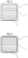
- Figs. 2 to 4 are plan views of a position of the infrared ray absorbing film according to the first embodiment of the present invention.
- n - -type silicon carbide substrate 1 an n - -type silicon carbide single crystal semiconductor substrate (hereinafter, referred to as "n - -type silicon carbide substrate") 1 is first prepared, that is formed from a silicon carbide four-layer-cycle hexagonal crystal (4H-SiC) and has an n - -type silicon carbide epitaxial layer deposited on one principal surface.
- n - -type silicon carbide substrate silicon carbide four-layer-cycle hexagonal crystal (4H-SiC) and has an n - -type silicon carbide epitaxial layer deposited on one principal surface.
- a p-type well region 2, and a p-type contact region 3 and an n-type source region 4 inside the p-type well region 2 are formed in the n - -type silicon carbide substrate (a surface layer of the n - -type silicon carbide epitaxial layer) 1 by ion implantation.
- the n -type silicon carbide substrate 1 having formed thereon an ion implantation mask of a silicon oxide film and the like that includes openings corresponding to the regions is introduced into an ion implanting apparatus to perform the above ion implantation.
- An n-type region is formed by implanting phosphorus ions or nitrogen ions.
- a p-type region is formed by implanting aluminum ions and the like.
- the n-type or the p-type regions are thereby formed in the openings of the ion implantation mask in the n - -type silicon carbide substrate 1.
- the p-type well region 2, the p-type contact region 3, and the n-type source region 4 are formed.
- a p-type breakdown voltage ring portion 13 is formed to surround an active region that has p-type well regions concentrated therein (see Fig. 2 ).
- An area up to the region that has the p-type breakdown voltage ring portion 13 disposed therein constitutes an area of one silicon carbide semiconductor device (a MOSFET device), and plural devices are arranged on the single n - -type silicon carbide substrate 1.
- activation annealing is performed at a temperature of about 1700 degrees C in an inert atmosphere such as argon.
- a gate insulating film 5 is grown on a surface of the n - -type silicon carbide substrate 1 by thermal oxidation, and a polysilicon film is formed thereon using a chemical vapor deposition (CVD) method.
- a gate electrode 6 is formed in an area extending over adjacent p-type well regions 2, using a photolithography process.
- a patterned silicon oxide film may be formed in advance on portions in which the gate insulating film 5 is unnecessary such as on the p-type breakdown voltage ring portion 13.
- An interlayer insulating film 7 formed of a silicon oxide film is formed using the CVD method, and openings are disposed in the interlayer insulating film 7 on the n-type source region 4 and the p-type contact region 3 using a photolithography process.
- the openings of the interlayer insulating film 7 are also disposed on junction regions (not depicted) between the gate electrode 6 and an outlet electrode 11 of the gate electrode 6.
- An infrared ray absorbing film 8 is disposed on the interlayer insulating film 7.
- a material having infrared ray emissivity of 0.5 or higher for near infrared rays having wavelengths of about 0.8 ⁇ m to about 2.5 ⁇ m is used as a material used for the infrared ray absorbing film 8.
- titanium nitride, molybdenum nitride, tungsten nitride, chromium nitride, and carbon can be used.
- a structure in which a metal material and metal nitride are stacked on each other may be used to maintain the adhesiveness between the infrared ray absorbing film 8 and the interlayer insulating film 7 and to suppress generation of cracks in the infrared ray absorbing film.
- titanium is deposited on the interlayer insulating film 7 using Ar as a sputtering gas and thereafter, the sputtering gas is changed to a mixture gas of nitrogen and Ar and sputtering is performed to thereby deposit titanium nitride.
- the thickness of the infrared ray absorbing film 8 is a film thickness that enables the infrared ray absorbing film 8 to absorb the infrared rays, inhibits deformation such as cracking consequent heating, and is, preferably, about 10 nm to about 300 nm.
- the film can be deposited using a reactive sputtering method that uses a titanium (Ti) target and a mixture gas of argon (Ar) and nitrogen, a sputtering method that uses a titanium nitride target, a CVD method that uses titanium tetra chloride and an ammonia gas, and the like.
- the infrared ray absorbing film 8 is patterned to be formed in all or a portion of an area excluding a source contact electrode portion (an opening to expose the n-type source region 4 and the p-type contact region 3 inside an opening of the interlayer insulating film 7) 16, a gate contact electrode portion (an opening (not depicted) to dispose the junction region between the gate electrode 6 and the outlet electrode 11 of the gate electrode 6 in the opening of the interlayer insulating film 7), and a gap portion to maintain insulation between these electrodes.
- the junction region between the gate electrode 6 and the outlet electrode 11 of the gate electrode 6 is formed near an interface of the active region and the p-type breakdown voltage ring portion 13.
- the infrared ray absorbing film 8 is disposed in an active region excluding the source contact electrode portion 16 (see Fig. 1 ) (an active region inside the p-type breakdown voltage ring portion 13). As depicted in Fig. 3 , the infrared ray absorbing film 8 may be disposed on the chip region 14 overall excluding the source contact electrode portion 16. In addition, as depicted in Fig. 4 , the n - -type silicon carbide substrate 1 can also be heated evenly by using the infrared ray absorbing film 8 for the portions that cannot be used as the device (the chip region 14) such as the outer peripheral portions of a wafer 15 (shaded portions in Fig. 4 ).
- the patterning for the infrared ray absorbing film 8 can be performed by a photolithography process using wet etching or dry etching.
- a metal nitride film can be processed with high dimensional precision by dry etching using chlorine gas, four hydrogen fluoride (4HF), and the like.
- the infrared ray emissivity can be improved by roughening the surface (the front face) of the infrared ray absorbing film 8.
- the surface of the infrared ray absorbing film 8 can be made uneven by patterning the infrared ray absorbing film 8, removing thereafter the resist mask used in the patterning of the infrared ray absorbing film 8, and inserting again the wafer 15 into the dry etching apparatus to etch the wafer 15 for a short time.
- the surface of the infrared ray absorbing film 8 can be made uneven by roughening in advance the surface of the interlayer insulating film 7 disposed beneath the infrared ray absorbing film 8.
- the surface can be made uneven by patterning the interlayer insulating film 7, removing thereafter the resist mask used in the patterning of the interlayer insulating film 7, and inserting again the wafer 15 into the dry etching apparatus to etch the wafer 15 for a short time.
- the p-type contact film is formed using a sputtering method and the like, and a p-type contact pattern 9 is disposed on the p-type contact region 3 using photolithography.
- a Group 3B element such as boron (B) or indium (In) is can be used as a material of the p-type contact, preferably, Al is used because of ease of Al pattern formation.
- the thickness of the Al film exceeds 100 nm, alloying with the Ni film mainly occurs, obstructing the formation of the silicide.
- Ni film of 50 nm is deposited using a sputtering method and the like, and a Ni pattern 10 is formed using photolithography in an area covering the n-type source region 4 and the p-type contact region 3.
- the thickness of the Ni film is a thickness that enables the silicide to be formed with high efficiency and that provides excellent control of the dimensions by the patterning; a thickness of about 20 to about 100 nm is used.
- the wafer 15 is heated at about 1000 degrees C in an inert gas atmosphere or in a reduced-pressure atmosphere using an RTA method and Ni silicide of the Ni pattern 10 is thereby produced on the p-type contact region 3 and the n-type source region 4 to form the source contact electrode portion 16.
- the heating rate is 1 degree C per minute or higher.
- the heating rate is lower than 1 degree C per minute, the alloying of the Al film and the Ni film preferentially occurs, obstructing the formation of the silicide. Rates of temperature increases exceeding 25 degrees C per second are difficult to realize because the sample is affected by thermal shock, cracking occurs, and the like.
- the outlet electrode 11 of Al having a thickness of 5 ⁇ m is formed by patterning to cover the source contact electrode portion 16.
- the outlet electrode 11 is also disposed on the gate electrode 6 away from the source region and, the gate and the outlet electrodes 11 are driven independently.
- a multi-layered film of Ti and Ni is disposed on the back face of the n - -type silicon carbide substrate 1 to be used as a drain electrode (a back face electrode) 12 and the silicon carbide semiconductor device (the MOSFET device) is thereby fabricated.
- a double implantation MOSFET was fabricated according to the method of manufacturing a silicon carbide semiconductor device of the first embodiment.
- an n - -silicon carbide substrate 1 was prepared having an epitaxially grown high resistivity layer of an n-type doping concentration of 2 ⁇ 10 15 cm -3 and a thickness of 15 ⁇ m.
- An ion implantation mask made from a silicon oxide film having a thickness of 1.5 ⁇ m was formed and the p-type well region 2 was formed by implanting Al ions at a temperature of 500 degrees C.
- the doping concentration was set to be 1 ⁇ 10 16 cm -3 and the implantation depth was set to be 1 ⁇ m.
- An ion implantation mask was formed from a silicon oxide film having an opening in a center of the p-type well region 2 and Al ions were implanted to thereby form the p-type contact region 3.
- the doping concentration was set to be 1 ⁇ 10 18 cm -3 .
- a TLM (Transmission Line Model) pattern region to measure the contact resistivity of the p-type contact region 3 was formed near the device.
- the n - -type silicon carbide substrate 1 was inserted into an annealing furnace to perform an activation process for five minutes at 1700 degrees C in an Ar atmosphere.
- An ion implantation mask was formed from a silicon oxide film having an opening on the side of the p-type contact region 3 in the p-type well region 2 and phosphorus ions were implanted to thereby form the n-type source region 4 having a doping concentration of 1 ⁇ 10 19 cm -3 .
- the n - -type silicon carbide substrate 1 was again inserted into the annealing furnace to perform an activation process for 5 minutes at 1700 degrees C in an Ar atmosphere.
- the n - -type silicon carbide substrate 1 was inserted into a quartz tube to perform a thermal oxidation process at 1200 degrees C in an atmosphere caused to contain water vapor by causing oxygen to flow through pure water, and a silicon oxide film to be the gate insulating film 5 was grown on the surface of the n - -type silicon carbide substrate 1 (the surface of the n - -type silicon carbide epitaxial layer).
- the thickness of the silicon oxide film was set to be 700 A.
- a polysilicon film having a thickness of 0.5 ⁇ m and having phosphorus doped therein was formed using a CVD method and the polysilicon film was patterned by photolithography to form the gate electrode 6.
- the gate electrode 6 was formed extending from an area that extends over the p-type well region 2 adjacent thereto to an area between the n - -type silicon carbide substrate 1 and the n-type source region 4 of the p-type well region 2.
- a PSG (Phosphorus Silicon Glass) film having a thickness of 1 ⁇ m was disposed using the CVD method and the PSG film was patterned using photolithography to form the interlayer insulating film 7 in an area covering the gate electrode 6.
- the process steps of depositing the interlayer insulating film 7 ⁇ patterning to form the openings of the interlayer insulating film 7 ⁇ depositing the infrared ray absorbing film 8 ⁇ patterning of the infrared ray absorbing film 8 were performs as described above.
- a titanium nitride film, a molybdenum nitride film, a tungsten nitride film, a chromium nitride film, and a carbon film were disposed each having a thickness of 0.1 ⁇ m and as the infrared ray absorbing film 8.
- Sputtering was performed for each of the nitrides using an Ar gas and a sputtering target formed by firing a metal nitride. Sputtering was also performed for the carbon film using an Ar gas and the carbon target.
- Patterning was performed for each of the nitride films using chlorine and for the carbon film, using four hydrogen fluoride (4HF) as the etching gas, and the infrared ray absorbing film 8 was formed at positions excluding the source contact electrode portion 16, the gate contact electrode portion, and the TLM pattern region (exposed in the other opening of the interlayer insulting film 7 and not depicted).
- 4HF hydrogen fluoride
- Al film having a thickness of 15 nm was formed using a sputtering method and the Al film was patterned to remain on the p-type contact region 3 and the TLM pattern region, to become the p-type contact pattern 9 and an Al electrode pattern for the TLM measurement, respectively.
- the Al electrode patterns for the TLM measurement were each shaped into a rectangle of 100x200 ⁇ m and were arranged having gaps of 1 ⁇ m, 2 ⁇ m, 4 ⁇ m, 8 ⁇ m, and 32 ⁇ m.
- a Ni film of 60 nm was disposed using the sputtering method and the Ni film was patterned to remain on the source contact electrode portion 16 and the TLM pattern region, to become the Ni pattern 10 and the Ni electrode pattern for the TLM measurement, respectively.
- the Ni electrode pattern for the TLM measurement was set to be same as the Al electrode pattern for the TLM measurement.
- a Ni film was also disposed on the back side of the n - -type silicon carbide substrate 1 to have a thickness of 60 nm.
- n - -type silicon carbide substrate 1 was inserted into an RTA furnace, and silicide was formed using the Ni pattern 10 and the Ni electrode pattern for the TLM measurement by increasing the temperature to 1000 degrees C at 4 degrees C per second based on the measurement using a thermocouple installed on the carbon susceptor, in a nitrogen atmosphere and maintaining the temperature for 5 minutes to thereby form metal silicide films of Al and Ni.
- An Al film having a film thickness of 5 ⁇ m was disposed using a sputtering method to form a source contact pad, a gate contact pad, and an electrode pad for TLM (the outlet electrode) 11.
- a MOSFET device was produced according to the above process steps and measurement was conducted for the contact resistivity (the contact resistivity between the p-type contact region 3 and the p-type contact pattern 9) in the TLM pattern region.
- An average value was calculated from the measurements acquired in the wafer face, and a distribution of the contact resistivity was calculated using an equation, the maximum value ⁇ the minimum value / the maximum value + the minimum value .
- Fig. 5 is a comparison diagram of a case where the infrared ray absorbing film is disposed according to the first embodiment of the present invention and a case where no such infrared ray absorbing film is disposed.
- the contact resistivity was measured in the TLM region for the MOSFET device having the infrared ray absorbing film 8 disposed therein of the first embodiment and a MOSFET device produced according to the process steps identical those of the first embodiment and not having the infrared ray absorbing film 8 disposed therein.
- Fig. 5 the contact resistivity was measured in the TLM region for the MOSFET device having the infrared ray absorbing film 8 disposed therein of the first embodiment and a MOSFET device produced according to the process steps identical those of the first embodiment and not having the infrared ray absorbing film 8 disposed therein.
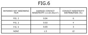
- Fig. 6 is a comparison diagram of the contact resistivity between a case where the infrared ray absorbing film is disposed according to a second embodiment of the present invention and a case where the infrared ray absorbing film is not disposed.
- titanium nitride films were disposed into the shapes (at the points) depicted in Fig. 2, Fig. 3 , and Fig. 4 , respectively as the infrared ray absorbing film 8.
- the dispersion of the contact resistivity of the p-type contact region 3 in the wafer face was measured using the TLM pattern region for measuring the contact resistivity near the device.
- a titanium nitride film to be the infrared ray absorbing film 8 was patterned into the shape depicted in Fig. 2 of the first embodiment, the n - -type silicon carbide substrate 1 was again inserted into the dry etching apparatus to perform dry etching for 5 seconds using a chlorine gas, and the surface of the infrared ray absorbing film 8 was thereby roughened. Using this wafer, the dispersion of the contact resistivity of the p-type contact region 3 in the wafer face was measured.
- the average value of the contact resistivity was further improved from that of the first embodiment to be 0.03 ⁇ 10 -2 cm 3 .
- a titanium nitride film to be the infrared ray absorbing film 8 was patterned into the shape depicted in Fig. 2 of the first embodiment.
- the heating rates were set to be 0.5 degrees C per second, 1.0 degree C per second, 4.0 degrees C per second, and 10 degrees C per second, and a cross-section of the source contact electrode portion 16 was cut off to check whether Ni silicide was formed.
- Figs. 7 and 8 are images of cross sections of the silicon carbide semiconductor device according to the fourth embodiment of the present invention.
- the silicon carbide semiconductor device depicted in Fig. 7 was produced with the heating rate of 0.5 degrees C per second and that in Fig. 8 was produced with the heating rate of 4.0 degrees C per second.
- a NiAl alloy was formed, divided into liquid-drop shapes on the n - -type silicon carbide substrate 1 (reference numeral "10" in Fig. 7 ).
- Compositional chemical analysis revealed that substantially no Ni silicide was formed therein, confirming this to be an example of poor Ni silicide formation.
- Fig. 9 is a table indicating presence/absence of Ni silicide formation according to heating rate, according to the fourth embodiment of the present invention. As depicted in Fig. 9 , a heating rate of 1 degree C per second or higher was necessary for the production of the Ni silicide.
- the metal silicide can be formed uniformly, dispersion of the contact resistivity can be prevented, and the properties and the reliability of the silicon carbide semiconductor device can be improved.
- the present invention is not limited to the above embodiments and various changes can be made thereto within a scope that does not depart from the spirit of the present invention.
- the present invention is further applicable when the p-type and the n-type are interchanged for each other or when the conductivity types of the silicon carbide substrate and the epitaxial layer grown on the principal surface of the silicon carbide substrate are set to be different from each other.
- a p-type contact pattern may be disposed to contact the p-type region to be the source region or the contact region
- a Ni pattern may be disposed to contact the n-type region to be the source region or the contact region.
- the semiconductor device according to the present invention is suitable for a vertical semiconductor apparatus in which electric current flows from the front face to the back face of the semiconductor substrate and is useful for, for example, a power semiconductor apparatus such as a power device and an industrial power semiconductor apparatus used for motor control or engine control.
Landscapes
- Electrodes Of Semiconductors (AREA)
Abstract
Description
- The present invention relates to a silicon carbide semiconductor device that uses silicon carbide (SiC) as a semiconductor material and in particular, causes electric current to flow from a front face of a semiconductor substrate to a back face thereof, and a method of manufacturing a silicon carbide semiconductor device.
- A silicon carbide semiconductor has a wider band gap compared to that of a silicon (Si) semiconductor and has therefore high breakdown electric field strength. "On-resistivity", which is resistivity in the conduction state, is inversely proportional to the cube of the breakdown electric field strength and therefore, in silicon carbide semiconductors (a four-layer-cycle hexagonal crystal: 4H-SiC) that are widely used and called 4-H types, the on-resistivity can be suppressed to be several-hundredths of that of a silicon semiconductor.
- With its property of high thermal conductivity that facilitates heat dissipation in addition to the above, the silicon carbide semiconductor is therefore expected to become a next-generation low-loss power semiconductor device. Silicon carbide semiconductor devices having various structures have been developed using the silicon carbide semiconductor such as, for example, a Schottky barrier diode, a MOSFET (an insulated gate field-effect transistor), a PN diode, an IGBT (an insulated gate bipolar transistor), and a GTO (a gate turnoff thyristor).
- On the other hand, concerning an ohmic electrode important in fabricating a silicon carbide semiconductor device, although it is clear that for an n-type region, excellent ohmic contact can be formed by using nickel (Ni) as the material of the ohmic electrode, for a p-type region, the material and a structure to form the ohmic contact are still under study. A multi-layered film of aluminum (Al) and Ni has been proposed as an example of an ohmic electrode in the p-type region (see, Non-Patent Literature 1).
- Non-Patent Literature 1: Ito, Kazuhiro, et al, "Simultaneous Formation of Ni/Al Ohmic Contacts to Both n-and p-Type 4H-SiC", Journal of ELECTRONIC MATERIALS, Vol. 37, No. 11, 2008, pp. 1674-1680
- An ohmic electrode is generally formed by forming a metal film on a silicon carbide semiconductor layer and thereafter, performing annealing under reduced pressure or in an inert gas atmosphere to produce a metal silicide. When a silicon carbide semiconductor device is produced, the annealing is generally performed at about 1000 degrees C. However, when annealing is performed for a multi-layered film of different metals such as the above film of Ni and Al, an alloy is produced between the metals without the formation of metal silicide between the silicon carbide semiconductor layer and the metal. A problem therefore arises in that this does not function as an ohmic electrode.
- A rapid annealing (RTA: Rapid Thermal Annealing) method is a method of efficiently producing a metal silicide. The RTA method is based on a mechanism that uses an infrared ray lamp to heat the substrate by a high heating rate, where the object to be heated is generally placed on a carbon susceptor because this annealing also efficiently heats materials having low infrared ray emissivity such as, for example, metal and synthetic quartz materials.
- When this mechanism is applied to the formation of a silicon carbide semiconductor device, a majority of the infrared rays from a halogen lamp used as the infrared ray lamp are absorbed by the carbon susceptor and not by the silicon carbide substrate because the silicon carbide semiconductor substrate does not absorb near-infrared rays of wavelengths up to about 2.5 µm. The silicon carbide substrate is heated by thermal conduction due to the contact with the susceptor. Temperature distributions occur on the front face of the silicon carbide substrate and at portions not in contact with the susceptor depending on the shape of the substrate and are the reason no metal silicide is formed.
- This uneven formation of the metal silicide causes variance in the contact resistivity and variance in the properties and the reliability of the device.
- In view of the above circumstances, one object of the present invention is to enable uniform formation of metal silicide, while minimizing the difference in the contact resistivity between the n-type region and the p-type region and obtaining long-term operating reliability.
- To achieve an object, a method of manufacturing a silicon carbide semiconductor device according to the present invention is characterized in that the method includes selectively forming an infrared ray absorbing film on a surface of a silicon carbide semiconductor substrate; sequentially forming on the silicon carbide semiconductor substrate, an aluminum film and a nickel film in an area excluding an area in which the infrared ray absorbing film is formed; and uniformly forming an electrode by a rapid annealing process with a predetermined heating rate on the silicon carbide semiconductor substrate.
- The method is further characterized in that at the rapid annealing process, the silicon carbide semiconductor substrate is placed on a carbon susceptor and heating is performed at an increasing temperature of at least 1 degree C per second with respect to a temperature measurement of the carbon susceptor.
- The method is characterized in that the method further includes roughening a surface of the infrared ray absorbing film.
- To achieve an object, a silicon carbide semiconductor device according to the present invention is characterized in that the silicon carbide semiconductor device includes an infrared ray absorbing film selectively formed on a surface of a silicon carbide semiconductor substrate; an aluminum film and a nickel film sequentially formed on the silicon carbide semiconductor substrate, in an area excluding an area in which the infrared ray absorbing film is formed; and an electrode uniformly formed on the silicon carbide semiconductor substrate, by a rapid annealing process with a predetermined heating rate.
- The silicon carbide semiconductor device is further characterized in that the infrared ray absorbing film is formed by at least one of titanium nitride, molybdenum nitride, tungsten nitride, chromium nitride, and a multi-layered film thereof.
- The silicon carbide semiconductor device is characterized in that the infrared ray absorbing film is formed by any one of a multi-layered film of titanium nitride and titanium, a multi-layered film of molybdenum nitride and molybdenum, a multi-layered film of tungsten nitride and tungsten, and a multi-layered film of chromium nitride and chromium.
- The silicon carbide semiconductor device is characterized in that the infrared ray absorbing film is formed having a thickness of at least 10 nm and no more than 300 nm.
- The silicon carbide semiconductor device is characterized in that the aluminum film is formed having a thickness of at least 10 nm and no more than 100 nm.
- The silicon carbide semiconductor device is characterized in that the nickel film is formed having a thickness of at least 20 nm and no more than 100 nm.
- The silicon carbide semiconductor device is characterized in that the infrared ray absorbing film is formed in an active region excluding a source contact electrode portion of a chip area.
- The silicon carbide semiconductor device is characterized in that the infrared ray absorbing film is formed in a chip area overall.
- The silicon carbide semiconductor device is characterized in that the infrared ray absorbing film is formed in an area excluding a chip area of a wafer.
- The silicon carbide semiconductor device is characterized in that the infrared ray absorbing film is formed in an area excluding an opening exposing an n-type region and a p-type region, among openings of an interlayer insulating film.
- The silicon carbide semiconductor device is characterized in that the nickel film is formed on the n-type region, and the aluminum film and the nickel film are stacked on the p-type region.
- According to the above configuration, metal silicide can be formed uniformly by using the infrared ray absorbing film and setting the heating rate in the RTA method to be a predetermined rate, and a higher performance silicon carbide semiconductor device can thereby be provided.
- According to the present invention, metal silicide can formed uniformly, the difference in the contact resistivity between the n-type region and the p-type region can be made small, and long-term operating reliability can be obtained.
-
-
Fig. 1 is a cross-sectional view of a silicon carbide semiconductor device having an infrared ray absorbing film disposed therein according to a first embodiment of the present invention; -
Fig. 2 is a plan view (part 1) of a position of the infrared ray absorbing film according to the first embodiment of the present invention; -
Fig. 3 is a plan view (part 2) of a position of the infrared ray absorbing film according to the first embodiment of the present invention; -
Fig. 4 is a plan view (part 3) of a position of the infrared ray absorbing film according to the first embodiment of the present invention; -
Fig. 5 is a comparison diagram of a case where the infrared ray absorbing film is disposed according to the first embodiment of the present invention and a case where no such infrared ray absorbing film is disposed; -
Fig. 6 is a comparison diagram of contact resistivity between a case where the infrared ray absorbing film is disposed according to a second embodiment of the present invention and a case where the infrared ray absorbing film is not disposed; -
Fig. 7 is an image of a cross-section of the silicon carbide semiconductor device according to a fourth embodiment of the present invention (example of poor Ni silicide formation); -
Fig. 8 is an image of a cross-section of the silicon carbide semiconductor device according to a fourth embodiment of the present invention (example of Ni silicide formation); and -
Fig. 9 is a table indicating presence/absence of Ni silicide formation according to heating rate, according to the fourth embodiment of the present invention. - Preferred embodiments of the present invention will be described in detail with reference to the accompanying drawings. In the present description and accompanying drawings, layers and regions prefixed with n or p mean that majority carriers are electrons or holes. Additionally, + or - appended to n or p means that the impurity concentration is higher or lower, respectively, than layers and regions without + or -. In the description of the embodiments below and the accompanying drawings, identical constituent elements will be given the same reference numerals and will not repeatedly be described.
- A method of manufacturing a silicon carbide semiconductor device according to a first embodiment of the present invention will be described taking an example of a case where a double implantation MOSFET (a DIMOSFET) is manufactured (produced) using a double implantation (Double Implante) process to form a p-type well region and an n-type source region by ion implantation.
Fig. 1 is a cross-sectional view of the silicon carbide semiconductor device having an infrared ray absorbing film disposed therein according to the first embodiment of the present invention.Figs. 2 to 4 are plan views of a position of the infrared ray absorbing film according to the first embodiment of the present invention. - For example, an n--type silicon carbide single crystal semiconductor substrate (hereinafter, referred to as "n--type silicon carbide substrate") 1 is first prepared, that is formed from a silicon carbide four-layer-cycle hexagonal crystal (4H-SiC) and has an n--type silicon carbide epitaxial layer deposited on one principal surface.
- A p-
type well region 2, and a p-type contact region 3 and an n-type source region 4 inside the p-type well region 2 are formed in the n--type silicon carbide substrate (a surface layer of the n--type silicon carbide epitaxial layer) 1 by ion implantation. When the p-type well region 2, the p-type contact region 3, and the n-type source region 4 are formed, the n--typesilicon carbide substrate 1 having formed thereon an ion implantation mask of a silicon oxide film and the like that includes openings corresponding to the regions is introduced into an ion implanting apparatus to perform the above ion implantation. An n-type region is formed by implanting phosphorus ions or nitrogen ions. A p-type region is formed by implanting aluminum ions and the like. The n-type or the p-type regions are thereby formed in the openings of the ion implantation mask in the n--typesilicon carbide substrate 1. By repeating this, the p-type well region 2, the p-type contact region 3, and the n-type source region 4 are formed. - A p-type breakdown
voltage ring portion 13 is formed to surround an active region that has p-type well regions concentrated therein (seeFig. 2 ). An area up to the region that has the p-type breakdownvoltage ring portion 13 disposed therein constitutes an area of one silicon carbide semiconductor device (a MOSFET device), and plural devices are arranged on the single n--typesilicon carbide substrate 1. - After removing the ion implantation mask, activation annealing is performed at a temperature of about 1700 degrees C in an inert atmosphere such as argon. A
gate insulating film 5 is grown on a surface of the n--typesilicon carbide substrate 1 by thermal oxidation, and a polysilicon film is formed thereon using a chemical vapor deposition (CVD) method. Agate electrode 6 is formed in an area extending over adjacent p-type well regions 2, using a photolithography process. A patterned silicon oxide film may be formed in advance on portions in which thegate insulating film 5 is unnecessary such as on the p-type breakdownvoltage ring portion 13. - An interlayer insulating
film 7 formed of a silicon oxide film is formed using the CVD method, and openings are disposed in theinterlayer insulating film 7 on the n-type source region 4 and the p-type contact region 3 using a photolithography process. The openings of theinterlayer insulating film 7 are also disposed on junction regions (not depicted) between thegate electrode 6 and anoutlet electrode 11 of thegate electrode 6. - An infrared
ray absorbing film 8 is disposed on theinterlayer insulating film 7. Preferably, a material having infrared ray emissivity of 0.5 or higher for near infrared rays having wavelengths of about 0.8 µm to about 2.5 µm is used as a material used for the infraredray absorbing film 8. For example, titanium nitride, molybdenum nitride, tungsten nitride, chromium nitride, and carbon can be used. - A structure in which a metal material and metal nitride are stacked on each other may be used to maintain the adhesiveness between the infrared
ray absorbing film 8 and theinterlayer insulating film 7 and to suppress generation of cracks in the infrared ray absorbing film. For example, titanium is deposited on theinterlayer insulating film 7 using Ar as a sputtering gas and thereafter, the sputtering gas is changed to a mixture gas of nitrogen and Ar and sputtering is performed to thereby deposit titanium nitride. - Preferably, the thickness of the infrared
ray absorbing film 8 is a film thickness that enables the infraredray absorbing film 8 to absorb the infrared rays, inhibits deformation such as cracking consequent heating, and is, preferably, about 10 nm to about 300 nm. For example, when titanium nitride is used as the infraredray absorbing film 8, the film can be deposited using a reactive sputtering method that uses a titanium (Ti) target and a mixture gas of argon (Ar) and nitrogen, a sputtering method that uses a titanium nitride target, a CVD method that uses titanium tetra chloride and an ammonia gas, and the like. - The infrared
ray absorbing film 8 is patterned to be formed in all or a portion of an area excluding a source contact electrode portion (an opening to expose the n-type source region 4 and the p-type contact region 3 inside an opening of the interlayer insulating film 7) 16, a gate contact electrode portion (an opening (not depicted) to dispose the junction region between thegate electrode 6 and theoutlet electrode 11 of thegate electrode 6 in the opening of the interlayer insulating film 7), and a gap portion to maintain insulation between these electrodes. The junction region between thegate electrode 6 and theoutlet electrode 11 of thegate electrode 6 is formed near an interface of the active region and the p-type breakdownvoltage ring portion 13. - As depicted in
Fig. 2 , in achip region 14, the infraredray absorbing film 8 is disposed in an active region excluding the source contact electrode portion 16 (seeFig. 1 ) (an active region inside the p-type breakdown voltage ring portion 13). As depicted inFig. 3 , the infraredray absorbing film 8 may be disposed on thechip region 14 overall excluding the sourcecontact electrode portion 16. In addition, as depicted inFig. 4 , the n--typesilicon carbide substrate 1 can also be heated evenly by using the infraredray absorbing film 8 for the portions that cannot be used as the device (the chip region 14) such as the outer peripheral portions of a wafer 15 (shaded portions inFig. 4 ). - The patterning for the infrared
ray absorbing film 8 can be performed by a photolithography process using wet etching or dry etching. For example, a metal nitride film can be processed with high dimensional precision by dry etching using chlorine gas, four hydrogen fluoride (4HF), and the like. - The infrared ray emissivity can be improved by roughening the surface (the front face) of the infrared
ray absorbing film 8. For example, the surface of the infraredray absorbing film 8 can be made uneven by patterning the infraredray absorbing film 8, removing thereafter the resist mask used in the patterning of the infraredray absorbing film 8, and inserting again thewafer 15 into the dry etching apparatus to etch thewafer 15 for a short time. - The surface of the infrared
ray absorbing film 8 can be made uneven by roughening in advance the surface of theinterlayer insulating film 7 disposed beneath the infraredray absorbing film 8. In this case, the surface can be made uneven by patterning theinterlayer insulating film 7, removing thereafter the resist mask used in the patterning of theinterlayer insulating film 7, and inserting again thewafer 15 into the dry etching apparatus to etch thewafer 15 for a short time. - Here, description with reference to
Fig. 1 is continued. The p-type contact film is formed using a sputtering method and the like, and a p-type contact pattern 9 is disposed on the p-type contact region 3 using photolithography. Although any Group 3B element such as boron (B) or indium (In) is can be used as a material of the p-type contact, preferably, Al is used because of ease of Al pattern formation. For example, in a case where Al is used and the thickness thereof is 5 nm or greater, lower contact resistivity with the p-type region is achieved compared to a case where only a Ni film is used, and when the thickness is 10 nm or greater, the dimensions of the Al pattern are more stable and the evenness of the contact resistivity in the wafer face is improved. When the thickness of the Al film exceeds 100 nm, alloying with the Ni film mainly occurs, obstructing the formation of the silicide. - An Ni film of 50 nm is deposited using a sputtering method and the like, and a
Ni pattern 10 is formed using photolithography in an area covering the n-type source region 4 and the p-type contact region 3. Preferably, the thickness of the Ni film is a thickness that enables the silicide to be formed with high efficiency and that provides excellent control of the dimensions by the patterning; a thickness of about 20 to about 100 nm is used. - The
wafer 15 is heated at about 1000 degrees C in an inert gas atmosphere or in a reduced-pressure atmosphere using an RTA method and Ni silicide of theNi pattern 10 is thereby produced on the p-type contact region 3 and the n-type source region 4 to form the sourcecontact electrode portion 16. Preferably, the heating rate is 1 degree C per minute or higher. When the heating rate is lower than 1 degree C per minute, the alloying of the Al film and the Ni film preferentially occurs, obstructing the formation of the silicide. Rates of temperature increases exceeding 25 degrees C per second are difficult to realize because the sample is affected by thermal shock, cracking occurs, and the like. - The
outlet electrode 11 of Al having a thickness of 5 µm is formed by patterning to cover the sourcecontact electrode portion 16. Theoutlet electrode 11 is also disposed on thegate electrode 6 away from the source region and, the gate and theoutlet electrodes 11 are driven independently. A multi-layered film of Ti and Ni is disposed on the back face of the n--typesilicon carbide substrate 1 to be used as a drain electrode (a back face electrode) 12 and the silicon carbide semiconductor device (the MOSFET device) is thereby fabricated. - A double implantation MOSFET was fabricated according to the method of manufacturing a silicon carbide semiconductor device of the first embodiment. For example, an n--
silicon carbide substrate 1 was prepared having an epitaxially grown high resistivity layer of an n-type doping concentration of 2×1015 cm-3 and a thickness of 15 µm. An ion implantation mask made from a silicon oxide film having a thickness of 1.5 µm was formed and the p-type well region 2 was formed by implanting Al ions at a temperature of 500 degrees C. The doping concentration was set to be 1×1016 cm-3 and the implantation depth was set to be 1 µm. - An ion implantation mask was formed from a silicon oxide film having an opening in a center of the p-
type well region 2 and Al ions were implanted to thereby form the p-type contact region 3. The doping concentration was set to be 1×1018 cm-3. Simultaneously, a TLM (Transmission Line Model) pattern region to measure the contact resistivity of the p-type contact region 3 was formed near the device. - The n--type
silicon carbide substrate 1 was inserted into an annealing furnace to perform an activation process for five minutes at 1700 degrees C in an Ar atmosphere. An ion implantation mask was formed from a silicon oxide film having an opening on the side of the p-type contact region 3 in the p-type well region 2 and phosphorus ions were implanted to thereby form the n-type source region 4 having a doping concentration of 1×1019 cm-3. - The n--type
silicon carbide substrate 1 was again inserted into the annealing furnace to perform an activation process for 5 minutes at 1700 degrees C in an Ar atmosphere. The n--typesilicon carbide substrate 1 was inserted into a quartz tube to perform a thermal oxidation process at 1200 degrees C in an atmosphere caused to contain water vapor by causing oxygen to flow through pure water, and a silicon oxide film to be thegate insulating film 5 was grown on the surface of the n--type silicon carbide substrate 1 (the surface of the n--type silicon carbide epitaxial layer). The thickness of the silicon oxide film was set to be 700 A. - A polysilicon film having a thickness of 0.5 µm and having phosphorus doped therein was formed using a CVD method and the polysilicon film was patterned by photolithography to form the
gate electrode 6. Thegate electrode 6 was formed extending from an area that extends over the p-type well region 2 adjacent thereto to an area between the n--typesilicon carbide substrate 1 and the n-type source region 4 of the p-type well region 2. - A PSG (Phosphorus Silicon Glass) film having a thickness of 1 µm was disposed using the CVD method and the PSG film was patterned using photolithography to form the
interlayer insulating film 7 in an area covering thegate electrode 6. The process steps of depositing theinterlayer insulating film 7 → patterning to form the openings of theinterlayer insulating film 7 → depositing the infraredray absorbing film 8 → patterning of the infraredray absorbing film 8 were performs as described above. - A titanium nitride film, a molybdenum nitride film, a tungsten nitride film, a chromium nitride film, and a carbon film were disposed each having a thickness of 0.1 µm and as the infrared
ray absorbing film 8. Sputtering was performed for each of the nitrides using an Ar gas and a sputtering target formed by firing a metal nitride. Sputtering was also performed for the carbon film using an Ar gas and the carbon target. Patterning was performed for each of the nitride films using chlorine and for the carbon film, using four hydrogen fluoride (4HF) as the etching gas, and the infraredray absorbing film 8 was formed at positions excluding the sourcecontact electrode portion 16, the gate contact electrode portion, and the TLM pattern region (exposed in the other opening of the interlayerinsulting film 7 and not depicted). - An Al film having a thickness of 15 nm was formed using a sputtering method and the Al film was patterned to remain on the p-
type contact region 3 and the TLM pattern region, to become the p-type contact pattern 9 and an Al electrode pattern for the TLM measurement, respectively. The Al electrode patterns for the TLM measurement were each shaped into a rectangle of 100x200 µm and were arranged having gaps of 1 µm, 2 µm, 4 µm, 8 µm, and 32 µm. - A Ni film of 60 nm was disposed using the sputtering method and the Ni film was patterned to remain on the source
contact electrode portion 16 and the TLM pattern region, to become theNi pattern 10 and the Ni electrode pattern for the TLM measurement, respectively. The Ni electrode pattern for the TLM measurement was set to be same as the Al electrode pattern for the TLM measurement. A Ni film was also disposed on the back side of the n--typesilicon carbide substrate 1 to have a thickness of 60 nm. - The n--type
silicon carbide substrate 1 was inserted into an RTA furnace, and silicide was formed using theNi pattern 10 and the Ni electrode pattern for the TLM measurement by increasing the temperature to 1000 degrees C at 4 degrees C per second based on the measurement using a thermocouple installed on the carbon susceptor, in a nitrogen atmosphere and maintaining the temperature for 5 minutes to thereby form metal silicide films of Al and Ni. - An Al film having a film thickness of 5 µm was disposed using a sputtering method to form a source contact pad, a gate contact pad, and an electrode pad for TLM (the outlet electrode) 11.
- A 100-nm Ti film and a 200-nm gold (Au) film, as a back-
face electrode 12, were deposited on the back face of the n--typesilicon carbide substrate 1 using a thermal vapor deposition method. - A MOSFET device was produced according to the above process steps and measurement was conducted for the contact resistivity (the contact resistivity between the p-
type contact region 3 and the p-type contact pattern 9) in the TLM pattern region. An average value was calculated from the measurements acquired in the wafer face, and a distribution of the contact resistivity was calculated using an equation,
-
Fig. 5 is a comparison diagram of a case where the infrared ray absorbing film is disposed according to the first embodiment of the present invention and a case where no such infrared ray absorbing film is disposed. As depicted inFig. 5 , the contact resistivity was measured in the TLM region for the MOSFET device having the infraredray absorbing film 8 disposed therein of the first embodiment and a MOSFET device produced according to the process steps identical those of the first embodiment and not having the infraredray absorbing film 8 disposed therein. As depicted inFig. 5 , it was confirmed that both the contact resistivity (the average value) and the contact resistivity distribution were reduced by disposing the infraredray absorbing film 8 using each of the various materials, as compared to the case where the infraredray absorbing film 8 was not disposed. -
Fig. 6 is a comparison diagram of the contact resistivity between a case where the infrared ray absorbing film is disposed according to a second embodiment of the present invention and a case where the infrared ray absorbing film is not disposed. In the second embodiment, at the process steps identical to those of the first embodiment, titanium nitride films were disposed into the shapes (at the points) depicted inFig. 2, Fig. 3 , andFig. 4 , respectively as the infraredray absorbing film 8. The dispersion of the contact resistivity of the p-type contact region 3 in the wafer face was measured using the TLM pattern region for measuring the contact resistivity near the device. - As depicted in
Fig. 6 , it was confirmed that both the contact resistivity (the average value) and the contact resistivity distribution were reduced by expanding the area of the infraredray absorbing film 8 irrespective of the point (inFigs. 2 to 4 ) where the infraredray absorbing film 8 is disposed. - In a third embodiment, at the process steps identical to those of the first embodiment, a titanium nitride film to be the infrared
ray absorbing film 8, was patterned into the shape depicted inFig. 2 of the first embodiment, the n--typesilicon carbide substrate 1 was again inserted into the dry etching apparatus to perform dry etching for 5 seconds using a chlorine gas, and the surface of the infraredray absorbing film 8 was thereby roughened. Using this wafer, the dispersion of the contact resistivity of the p-type contact region 3 in the wafer face was measured. - As a result, it was confirmed that the average value of the contact resistivity was further improved from that of the first embodiment to be 0.03×10⁻² cm3.
- In a fourth embodiment, at the process steps identical to those of the first embodiment, a titanium nitride film to be the infrared
ray absorbing film 8, was patterned into the shape depicted inFig. 2 of the first embodiment. In the RTA after the disposition of the Ni, samples were fabricated for which the heating rates were set to be 0.5 degrees C per second, 1.0 degree C per second, 4.0 degrees C per second, and 10 degrees C per second, and a cross-section of the sourcecontact electrode portion 16 was cut off to check whether Ni silicide was formed. -
Figs. 7 and8 are images of cross sections of the silicon carbide semiconductor device according to the fourth embodiment of the present invention. The silicon carbide semiconductor device depicted inFig. 7 was produced with the heating rate of 0.5 degrees C per second and that inFig. 8 was produced with the heating rate of 4.0 degrees C per second. In the case where the heating rate was low depicted inFig. 7 , a NiAl alloy was formed, divided into liquid-drop shapes on the n--type silicon carbide substrate 1 (reference numeral "10" inFig. 7 ). Compositional chemical analysis revealed that substantially no Ni silicide was formed therein, confirming this to be an example of poor Ni silicide formation. On the other hand, in the case where the heating rate was 4 degrees C per second as depicted inFig. 8 , it was confirmed that the Ni silicide was formed continuously in the entire source contact electrode portion 16 (reference numeral "10" inFig. 8 ). -
Fig. 9 is a table indicating presence/absence of Ni silicide formation according to heating rate, according to the fourth embodiment of the present invention. As depicted inFig. 9 , a heating rate of 1 degree C per second or higher was necessary for the production of the Ni silicide. - According to each of the above embodiments, the metal silicide can be formed uniformly, dispersion of the contact resistivity can be prevented, and the properties and the reliability of the silicon carbide semiconductor device can be improved.
- The present invention is not limited to the above embodiments and various changes can be made thereto within a scope that does not depart from the spirit of the present invention. For example, the present invention is further applicable when the p-type and the n-type are interchanged for each other or when the conductivity types of the silicon carbide substrate and the epitaxial layer grown on the principal surface of the silicon carbide substrate are set to be different from each other. In this case, a p-type contact pattern may be disposed to contact the p-type region to be the source region or the contact region, and a Ni pattern may be disposed to contact the n-type region to be the source region or the contact region.
- As described, the semiconductor device according to the present invention is suitable for a vertical semiconductor apparatus in which electric current flows from the front face to the back face of the semiconductor substrate and is useful for, for example, a power semiconductor apparatus such as a power device and an industrial power semiconductor apparatus used for motor control or engine control.
-
- 1
- n--type silicon carbide substrate
- 2
- p-type well region
- 3
- p-type contact region
- 4
- n-type source region
- 5
- gate insulating film
- 6
- gate electrode
- 7
- interlayer insulating film
- 8
- infrared ray absorbing film
- 9
- p-type contact pattern
- 10
- Ni pattern
- 11
- outlet electrode
- 12
- back face electrode
- 13
- p-type breakdown voltage ring portion
- 14
- chip region
- 15
- wafer
Claims (14)
- A method of manufacturing a silicon carbide semiconductor device, the method comprising:selectively forming an infrared ray absorbing film on a surface of a silicon carbide semiconductor substrate;sequentially forming on the silicon carbide semiconductor substrate, an aluminum film and a nickel film in an area excluding an area in which the infrared ray absorbing film is formed; anduniformly forming an electrode by a rapid annealing process with a predetermined heating rate on the silicon carbide semiconductor substrate.
- The method according to claim 1, wherein
at the rapid annealing process, the silicon carbide semiconductor substrate is placed on a carbon susceptor and heating is performed at an increasing temperature of at least 1 degree C per second with respect to a temperature measurement of the carbon susceptor. - The method according to claim 1 or 2, further comprising
roughening a surface of the infrared ray absorbing film. - A silicon carbide semiconductor device comprising:an infrared ray absorbing film selectively formed on a surface of a silicon carbide semiconductor substrate;an aluminum film and a nickel film sequentially formed on the silicon carbide semiconductor substrate, in an area excluding an area in which the infrared ray absorbing film is formed; andan electrode uniformly formed on the silicon carbide semiconductor substrate, by a rapid annealing process with a predetermined heating rate.
- The silicon carbide semiconductor device according to claim 4, wherein
the infrared ray absorbing film is formed by at least one of titanium nitride, molybdenum nitride, tungsten nitride, chromium nitride, and a multi-layered film thereof. - The silicon carbide semiconductor device according to claim 4, wherein
the infrared ray absorbing film is formed by any one of a multi-layered film of titanium nitride and titanium, a multi-layered film of molybdenum nitride and molybdenum, a multi-layered film of tungsten nitride and tungsten, and a multi-layered film of chromium nitride and chromium. - The silicon carbide semiconductor device according to claim 4, wherein
the infrared ray absorbing film is formed having a thickness of at least 10 nm and no more than 300 nm. - The silicon carbide semiconductor device according to claim 4, wherein
the aluminum film is formed having a thickness of at least 10 nm and no more than 100 nm. - The silicon carbide semiconductor device according to claim 4, wherein
the nickel film is formed having a thickness of at least 20 nm and no more than 100 nm. - The silicon carbide semiconductor device according to claim 4, wherein
the infrared ray absorbing film is formed in an active region excluding a source contact electrode portion of a chip area. - The silicon carbide semiconductor device according to claim 4, wherein
the infrared ray absorbing film is formed in a chip area overall. - The silicon carbide semiconductor device according to claim 4, wherein
the infrared ray absorbing film is formed in an area excluding a chip area of a wafer. - The silicon carbide semiconductor device according to any one of claims 4 to 12, wherein
the infrared ray absorbing film is formed in an area excluding an opening exposing an n-type region and a p-type region, among openings of an interlayer insulating film. - The silicon carbide semiconductor device according to claim 13, wherein
the nickel film is formed on the n-type region, and the aluminum film and the nickel film are stacked on the p-type region.
Applications Claiming Priority (2)
| Application Number | Priority Date | Filing Date | Title |
|---|---|---|---|
| JP2013184515 | 2013-09-05 | ||
| PCT/JP2014/071122 WO2015033740A1 (en) | 2013-09-05 | 2014-08-08 | Silicon carbide semiconductor element and method for manufacturing silicon carbide semiconductor element |
Publications (3)
| Publication Number | Publication Date |
|---|---|
| EP3043376A1 true EP3043376A1 (en) | 2016-07-13 |
| EP3043376A4 EP3043376A4 (en) | 2017-04-12 |
| EP3043376B1 EP3043376B1 (en) | 2021-03-03 |
Family
ID=52628223
Family Applications (1)
| Application Number | Title | Priority Date | Filing Date |
|---|---|---|---|
| EP14842165.4A Active EP3043376B1 (en) | 2013-09-05 | 2014-08-08 | Method for manufacturing silicon carbide semiconductor element |
Country Status (5)
| Country | Link |
|---|---|
| US (1) | US9923062B2 (en) |
| EP (1) | EP3043376B1 (en) |
| JP (1) | JP5885284B2 (en) |
| CN (1) | CN105493245B (en) |
| WO (1) | WO2015033740A1 (en) |
Families Citing this family (9)
| Publication number | Priority date | Publication date | Assignee | Title |
|---|---|---|---|---|
| JP6480860B2 (en) * | 2013-03-29 | 2019-03-13 | 富士電機株式会社 | Semiconductor device and method of manufacturing semiconductor device |
| JP6582537B2 (en) * | 2015-05-13 | 2019-10-02 | 富士電機株式会社 | Semiconductor device and manufacturing method of semiconductor device |
| JP6617546B2 (en) * | 2015-12-11 | 2019-12-11 | 富士電機株式会社 | Semiconductor device and manufacturing method of semiconductor device |
| JP6690333B2 (en) * | 2016-03-16 | 2020-04-28 | 富士電機株式会社 | Silicon carbide semiconductor device and method for manufacturing silicon carbide semiconductor device |
| US10466108B2 (en) * | 2017-08-24 | 2019-11-05 | United States Of America As Represented By The Administrator Of Nasa | Molybdenum nitride absorber coating for a detector |
| TWI693642B (en) * | 2017-12-22 | 2020-05-11 | 美商雷森公司 | Method for controlling the amount of radiation having a predetermined wavelength to be absorbed by a structure disposed on a semiconductor |
| JP2022047759A (en) * | 2020-09-14 | 2022-03-25 | 株式会社Screenホールディングス | Metal wiring formation method |
| CN115394647A (en) * | 2022-07-22 | 2022-11-25 | 浙江大学杭州国际科创中心 | Silicon carbide semiconductor ohmic contact annealing method |
| CN117684138B (en) * | 2023-12-08 | 2026-01-20 | 中国航发北京航空材料研究院 | Preparation method of ceramic oxide film thermocouple for aeroengine temperature measurement |
Family Cites Families (16)
| Publication number | Priority date | Publication date | Assignee | Title |
|---|---|---|---|---|
| US5580388A (en) * | 1993-01-21 | 1996-12-03 | Moore Epitaxial, Inc. | Multi-layer susceptor for rapid thermal process reactors |
| DE10051049B4 (en) * | 2000-10-14 | 2011-04-07 | Cree, Inc. | Aluminum-nickel contact metallization for p-doped SiC and manufacturing process therefor |
| US6794684B2 (en) * | 2001-02-01 | 2004-09-21 | Cree, Inc. | Reflective ohmic contacts for silicon carbide including a layer consisting essentially of nickel, methods of fabricating same, and light emitting devices including the same |
| FR2827855B1 (en) * | 2001-07-25 | 2004-07-02 | Saint Gobain | GLAZING PROVIDED WITH A STACK OF THIN FILMS REFLECTING INFRARED AND / OR SOLAR RADIATION |
| JP2003086534A (en) * | 2001-09-10 | 2003-03-20 | Nissan Motor Co Ltd | Ohmic electrode structure of silicon carbide semiconductor and method of manufacturing ohmic electrode of silicon carbide semiconductor |
| JP2003229565A (en) * | 2002-02-04 | 2003-08-15 | Mitsubishi Electric Corp | Semiconductor device and method of manufacturing the same |
| JP2007059646A (en) * | 2005-08-25 | 2007-03-08 | Denso Corp | Manufacturing method of semiconductor device |
| JP2007101213A (en) | 2005-09-30 | 2007-04-19 | Ricoh Co Ltd | Semiconductor device, infrared sensor, and method of manufacturing semiconductor device |
| JP2007149984A (en) * | 2005-11-28 | 2007-06-14 | Rohm Co Ltd | Manufacture of nitride semiconductor light-emitting element |
| JP2008204972A (en) * | 2007-02-16 | 2008-09-04 | Matsushita Electric Ind Co Ltd | Semiconductor device and manufacturing method thereof |
| FR2914488B1 (en) * | 2007-03-30 | 2010-08-27 | Soitec Silicon On Insulator | DOPE HEATING SUBSTRATE |
| CN101927976B (en) * | 2009-09-30 | 2013-09-25 | 浙江大立科技股份有限公司 | Infrared detector with micro-bridge structure and manufacturing method thereof |
| JPWO2011115294A1 (en) | 2010-03-16 | 2013-07-04 | 合同会社先端配線材料研究所 | Silicon carbide electrode, silicon carbide semiconductor element, silicon carbide semiconductor device, and method for forming silicon carbide electrode |
| JP5554126B2 (en) * | 2010-04-06 | 2014-07-23 | 三菱電機株式会社 | Method for manufacturing SiC semiconductor device |
| JP5756692B2 (en) * | 2011-07-05 | 2015-07-29 | 株式会社日立製作所 | Manufacturing method of semiconductor device |
| JP5728339B2 (en) * | 2011-09-08 | 2015-06-03 | 株式会社東芝 | Semiconductor device and manufacturing method of semiconductor device |
-
2014
- 2014-08-08 WO PCT/JP2014/071122 patent/WO2015033740A1/en not_active Ceased
- 2014-08-08 CN CN201480048187.0A patent/CN105493245B/en active Active
- 2014-08-08 EP EP14842165.4A patent/EP3043376B1/en active Active
- 2014-08-08 JP JP2015525333A patent/JP5885284B2/en active Active
-
2016
- 2016-03-01 US US15/058,139 patent/US9923062B2/en active Active
Non-Patent Citations (1)
| Title |
|---|
| See references of WO2015033740A1 * |
Also Published As
| Publication number | Publication date |
|---|---|
| WO2015033740A1 (en) | 2015-03-12 |
| JPWO2015033740A1 (en) | 2017-03-02 |
| US9923062B2 (en) | 2018-03-20 |
| CN105493245A (en) | 2016-04-13 |
| US20160181376A1 (en) | 2016-06-23 |
| EP3043376A4 (en) | 2017-04-12 |
| CN105493245B (en) | 2018-01-16 |
| EP3043376B1 (en) | 2021-03-03 |
| JP5885284B2 (en) | 2016-03-15 |
Similar Documents
| Publication | Publication Date | Title |
|---|---|---|
| EP3043376B1 (en) | Method for manufacturing silicon carbide semiconductor element | |
| US8697555B2 (en) | Method of producing semiconductor device and semiconductor device | |
| JP5525940B2 (en) | Semiconductor device and manufacturing method of semiconductor device | |
| JP4412335B2 (en) | Method for manufacturing silicon carbide semiconductor device | |
| US8367507B1 (en) | Manufacturing method of semiconductor device | |
| US8564017B2 (en) | Silicon carbide semiconductor device and method for manufacturing same | |
| US9543395B2 (en) | Normally-off power JFET and manufacturing method thereof | |
| US20120193643A1 (en) | Semiconductor device | |
| US8847238B2 (en) | Semiconductor device which can withstand high voltage or high current and method for fabricating the same | |
| US8476733B2 (en) | Semiconductor element and manufacturing method therefor | |
| US9613809B2 (en) | Method of manufacturing silicon carbide semiconductor device | |
| JP7047250B2 (en) | Manufacturing method of silicon carbide semiconductor device | |
| JP2011035322A (en) | Semiconductor device and method of manufacturing the same | |
| JP6208106B2 (en) | Semiconductor device and manufacturing method thereof | |
| US9978598B2 (en) | Silicon carbide semiconductor device and method of manufacturing silicon carbide semiconductor device | |
| JP2013058668A (en) | Semiconductor element and manufacturing method therefor | |
| US8796123B2 (en) | Method of manufacturing silicon carbide semiconductor device | |
| JP6441412B2 (en) | Semiconductor device | |
| EP3783661A1 (en) | Semiconductor device and method of manufacturing same | |
| JP6822088B2 (en) | Silicon Carbide Semiconductor Device and Method for Manufacturing Silicon Carbide Semiconductor Device | |
| US20250212444A1 (en) | Semiconductor device and method for manufacturing the same | |
| JP2024092776A (en) | Silicon carbide wafer and silicon carbide semiconductor device using same | |
| JP2023115046A (en) | SiC wafer and its manufacturing method | |
| JP2010027638A (en) | Fabrication process of semiconductor device and semiconductor device |
Legal Events
| Date | Code | Title | Description |
|---|---|---|---|
| PUAI | Public reference made under article 153(3) epc to a published international application that has entered the european phase |
Free format text: ORIGINAL CODE: 0009012 |
|
| 17P | Request for examination filed |
Effective date: 20160225 |
|
| AK | Designated contracting states |
Kind code of ref document: A1 Designated state(s): AL AT BE BG CH CY CZ DE DK EE ES FI FR GB GR HR HU IE IS IT LI LT LU LV MC MK MT NL NO PL PT RO RS SE SI SK SM TR |
|
| AX | Request for extension of the european patent |
Extension state: BA ME |
|
| RIN1 | Information on inventor provided before grant (corrected) |
Inventor name: OKAMOTO, MITSUO Inventor name: UTSUMI, MAKOTO Inventor name: FUKUDA, KENJI Inventor name: SAKAI, YOSHIYUKI Inventor name: HARADA, SHINSUKE |
|
| DAX | Request for extension of the european patent (deleted) | ||
| A4 | Supplementary search report drawn up and despatched |
Effective date: 20170309 |
|
| RIC1 | Information provided on ipc code assigned before grant |
Ipc: H01L 29/78 20060101ALI20170303BHEP Ipc: H01L 21/26 20060101ALI20170303BHEP Ipc: H01L 21/28 20060101AFI20170303BHEP Ipc: H01L 29/12 20060101ALI20170303BHEP Ipc: H01L 21/336 20060101ALI20170303BHEP Ipc: H01L 29/06 20060101ALI20170303BHEP |
|
| STAA | Information on the status of an ep patent application or granted ep patent |
Free format text: STATUS: EXAMINATION IS IN PROGRESS |
|
| 17Q | First examination report despatched |
Effective date: 20200130 |
|
| RIC1 | Information provided on ipc code assigned before grant |
Ipc: H01L 21/04 20060101ALI20200609BHEP Ipc: H01L 29/78 20060101ALI20200609BHEP Ipc: H01L 21/324 20060101ALI20200609BHEP Ipc: H01L 21/28 20060101AFI20200609BHEP Ipc: H01L 29/06 20060101ALI20200609BHEP Ipc: H01L 29/16 20060101ALI20200609BHEP Ipc: H01L 21/26 20060101ALI20200609BHEP Ipc: H01L 21/336 20060101ALI20200609BHEP |
|
| GRAP | Despatch of communication of intention to grant a patent |
Free format text: ORIGINAL CODE: EPIDOSNIGR1 |
|
| STAA | Information on the status of an ep patent application or granted ep patent |
Free format text: STATUS: GRANT OF PATENT IS INTENDED |
|
| INTG | Intention to grant announced |
Effective date: 20200915 |
|
| RIN1 | Information on inventor provided before grant (corrected) |
Inventor name: OKAMOTO, MITSUO Inventor name: SAKAI, YOSHIYUKI Inventor name: HARADA, SHINSUKE Inventor name: FUKUDA, KENJI Inventor name: UTSUMI, MAKOTO |
|
| GRAS | Grant fee paid |
Free format text: ORIGINAL CODE: EPIDOSNIGR3 |
|
| GRAA | (expected) grant |
Free format text: ORIGINAL CODE: 0009210 |
|
| STAA | Information on the status of an ep patent application or granted ep patent |
Free format text: STATUS: THE PATENT HAS BEEN GRANTED |
|
| RAP1 | Party data changed (applicant data changed or rights of an application transferred) |
Owner name: FUJI ELECTRIC CO., LTD. |
|
| AK | Designated contracting states |
Kind code of ref document: B1 Designated state(s): AL AT BE BG CH CY CZ DE DK EE ES FI FR GB GR HR HU IE IS IT LI LT LU LV MC MK MT NL NO PL PT RO RS SE SI SK SM TR |
|
| REG | Reference to a national code |
Ref country code: GB Ref legal event code: FG4D |
|
| REG | Reference to a national code |
Ref country code: AT Ref legal event code: REF Ref document number: 1368130 Country of ref document: AT Kind code of ref document: T Effective date: 20210315 Ref country code: CH Ref legal event code: EP |
|
| REG | Reference to a national code |
Ref country code: DE Ref legal event code: R096 Ref document number: 602014075427 Country of ref document: DE |
|
| REG | Reference to a national code |
Ref country code: IE Ref legal event code: FG4D |
|
| REG | Reference to a national code |
Ref country code: LT Ref legal event code: MG9D |
|
| PG25 | Lapsed in a contracting state [announced via postgrant information from national office to epo] |
Ref country code: NO Free format text: LAPSE BECAUSE OF FAILURE TO SUBMIT A TRANSLATION OF THE DESCRIPTION OR TO PAY THE FEE WITHIN THE PRESCRIBED TIME-LIMIT Effective date: 20210603 Ref country code: BG Free format text: LAPSE BECAUSE OF FAILURE TO SUBMIT A TRANSLATION OF THE DESCRIPTION OR TO PAY THE FEE WITHIN THE PRESCRIBED TIME-LIMIT Effective date: 20210603 Ref country code: GR Free format text: LAPSE BECAUSE OF FAILURE TO SUBMIT A TRANSLATION OF THE DESCRIPTION OR TO PAY THE FEE WITHIN THE PRESCRIBED TIME-LIMIT Effective date: 20210604 Ref country code: FI Free format text: LAPSE BECAUSE OF FAILURE TO SUBMIT A TRANSLATION OF THE DESCRIPTION OR TO PAY THE FEE WITHIN THE PRESCRIBED TIME-LIMIT Effective date: 20210303 Ref country code: HR Free format text: LAPSE BECAUSE OF FAILURE TO SUBMIT A TRANSLATION OF THE DESCRIPTION OR TO PAY THE FEE WITHIN THE PRESCRIBED TIME-LIMIT Effective date: 20210303 Ref country code: LT Free format text: LAPSE BECAUSE OF FAILURE TO SUBMIT A TRANSLATION OF THE DESCRIPTION OR TO PAY THE FEE WITHIN THE PRESCRIBED TIME-LIMIT Effective date: 20210303 |
|
| REG | Reference to a national code |
Ref country code: NL Ref legal event code: MP Effective date: 20210303 |
|
| REG | Reference to a national code |
Ref country code: AT Ref legal event code: MK05 Ref document number: 1368130 Country of ref document: AT Kind code of ref document: T Effective date: 20210303 |
|
| PG25 | Lapsed in a contracting state [announced via postgrant information from national office to epo] |
Ref country code: SE Free format text: LAPSE BECAUSE OF FAILURE TO SUBMIT A TRANSLATION OF THE DESCRIPTION OR TO PAY THE FEE WITHIN THE PRESCRIBED TIME-LIMIT Effective date: 20210303 Ref country code: RS Free format text: LAPSE BECAUSE OF FAILURE TO SUBMIT A TRANSLATION OF THE DESCRIPTION OR TO PAY THE FEE WITHIN THE PRESCRIBED TIME-LIMIT Effective date: 20210303 Ref country code: LV Free format text: LAPSE BECAUSE OF FAILURE TO SUBMIT A TRANSLATION OF THE DESCRIPTION OR TO PAY THE FEE WITHIN THE PRESCRIBED TIME-LIMIT Effective date: 20210303 Ref country code: PL Free format text: LAPSE BECAUSE OF FAILURE TO SUBMIT A TRANSLATION OF THE DESCRIPTION OR TO PAY THE FEE WITHIN THE PRESCRIBED TIME-LIMIT Effective date: 20210303 |
|
| PG25 | Lapsed in a contracting state [announced via postgrant information from national office to epo] |
Ref country code: NL Free format text: LAPSE BECAUSE OF FAILURE TO SUBMIT A TRANSLATION OF THE DESCRIPTION OR TO PAY THE FEE WITHIN THE PRESCRIBED TIME-LIMIT Effective date: 20210303 |
|
| PG25 | Lapsed in a contracting state [announced via postgrant information from national office to epo] |
Ref country code: EE Free format text: LAPSE BECAUSE OF FAILURE TO SUBMIT A TRANSLATION OF THE DESCRIPTION OR TO PAY THE FEE WITHIN THE PRESCRIBED TIME-LIMIT Effective date: 20210303 Ref country code: CZ Free format text: LAPSE BECAUSE OF FAILURE TO SUBMIT A TRANSLATION OF THE DESCRIPTION OR TO PAY THE FEE WITHIN THE PRESCRIBED TIME-LIMIT Effective date: 20210303 Ref country code: AT Free format text: LAPSE BECAUSE OF FAILURE TO SUBMIT A TRANSLATION OF THE DESCRIPTION OR TO PAY THE FEE WITHIN THE PRESCRIBED TIME-LIMIT Effective date: 20210303 Ref country code: SM Free format text: LAPSE BECAUSE OF FAILURE TO SUBMIT A TRANSLATION OF THE DESCRIPTION OR TO PAY THE FEE WITHIN THE PRESCRIBED TIME-LIMIT Effective date: 20210303 |
|
| PG25 | Lapsed in a contracting state [announced via postgrant information from national office to epo] |
Ref country code: PT Free format text: LAPSE BECAUSE OF FAILURE TO SUBMIT A TRANSLATION OF THE DESCRIPTION OR TO PAY THE FEE WITHIN THE PRESCRIBED TIME-LIMIT Effective date: 20210705 Ref country code: ES Free format text: LAPSE BECAUSE OF FAILURE TO SUBMIT A TRANSLATION OF THE DESCRIPTION OR TO PAY THE FEE WITHIN THE PRESCRIBED TIME-LIMIT Effective date: 20210303 Ref country code: SK Free format text: LAPSE BECAUSE OF FAILURE TO SUBMIT A TRANSLATION OF THE DESCRIPTION OR TO PAY THE FEE WITHIN THE PRESCRIBED TIME-LIMIT Effective date: 20210303 Ref country code: RO Free format text: LAPSE BECAUSE OF FAILURE TO SUBMIT A TRANSLATION OF THE DESCRIPTION OR TO PAY THE FEE WITHIN THE PRESCRIBED TIME-LIMIT Effective date: 20210303 Ref country code: IS Free format text: LAPSE BECAUSE OF FAILURE TO SUBMIT A TRANSLATION OF THE DESCRIPTION OR TO PAY THE FEE WITHIN THE PRESCRIBED TIME-LIMIT Effective date: 20210703 |
|
| REG | Reference to a national code |
Ref country code: DE Ref legal event code: R097 Ref document number: 602014075427 Country of ref document: DE |
|
| PLBE | No opposition filed within time limit |
Free format text: ORIGINAL CODE: 0009261 |
|
| STAA | Information on the status of an ep patent application or granted ep patent |
Free format text: STATUS: NO OPPOSITION FILED WITHIN TIME LIMIT |
|
| PG25 | Lapsed in a contracting state [announced via postgrant information from national office to epo] |
Ref country code: DK Free format text: LAPSE BECAUSE OF FAILURE TO SUBMIT A TRANSLATION OF THE DESCRIPTION OR TO PAY THE FEE WITHIN THE PRESCRIBED TIME-LIMIT Effective date: 20210303 Ref country code: AL Free format text: LAPSE BECAUSE OF FAILURE TO SUBMIT A TRANSLATION OF THE DESCRIPTION OR TO PAY THE FEE WITHIN THE PRESCRIBED TIME-LIMIT Effective date: 20210303 |
|
| 26N | No opposition filed |
Effective date: 20211206 |
|
| PG25 | Lapsed in a contracting state [announced via postgrant information from national office to epo] |
Ref country code: SI Free format text: LAPSE BECAUSE OF FAILURE TO SUBMIT A TRANSLATION OF THE DESCRIPTION OR TO PAY THE FEE WITHIN THE PRESCRIBED TIME-LIMIT Effective date: 20210303 |
|
| REG | Reference to a national code |
Ref country code: CH Ref legal event code: PL |
|
| PG25 | Lapsed in a contracting state [announced via postgrant information from national office to epo] |
Ref country code: MC Free format text: LAPSE BECAUSE OF FAILURE TO SUBMIT A TRANSLATION OF THE DESCRIPTION OR TO PAY THE FEE WITHIN THE PRESCRIBED TIME-LIMIT Effective date: 20210303 |
|
| REG | Reference to a national code |
Ref country code: BE Ref legal event code: MM Effective date: 20210831 |
|
| GBPC | Gb: european patent ceased through non-payment of renewal fee |
Effective date: 20210808 |
|
| PG25 | Lapsed in a contracting state [announced via postgrant information from national office to epo] |
Ref country code: LI Free format text: LAPSE BECAUSE OF NON-PAYMENT OF DUE FEES Effective date: 20210831 Ref country code: IT Free format text: LAPSE BECAUSE OF FAILURE TO SUBMIT A TRANSLATION OF THE DESCRIPTION OR TO PAY THE FEE WITHIN THE PRESCRIBED TIME-LIMIT Effective date: 20210303 Ref country code: CH Free format text: LAPSE BECAUSE OF NON-PAYMENT OF DUE FEES Effective date: 20210831 |
|
| PG25 | Lapsed in a contracting state [announced via postgrant information from national office to epo] |
Ref country code: IS Free format text: LAPSE BECAUSE OF FAILURE TO SUBMIT A TRANSLATION OF THE DESCRIPTION OR TO PAY THE FEE WITHIN THE PRESCRIBED TIME-LIMIT Effective date: 20210703 Ref country code: LU Free format text: LAPSE BECAUSE OF NON-PAYMENT OF DUE FEES Effective date: 20210808 |
|
| PG25 | Lapsed in a contracting state [announced via postgrant information from national office to epo] |
Ref country code: IE Free format text: LAPSE BECAUSE OF NON-PAYMENT OF DUE FEES Effective date: 20210808 Ref country code: GB Free format text: LAPSE BECAUSE OF NON-PAYMENT OF DUE FEES Effective date: 20210808 Ref country code: FR Free format text: LAPSE BECAUSE OF NON-PAYMENT OF DUE FEES Effective date: 20210831 Ref country code: BE Free format text: LAPSE BECAUSE OF NON-PAYMENT OF DUE FEES Effective date: 20210831 |
|
| PG25 | Lapsed in a contracting state [announced via postgrant information from national office to epo] |
Ref country code: HU Free format text: LAPSE BECAUSE OF FAILURE TO SUBMIT A TRANSLATION OF THE DESCRIPTION OR TO PAY THE FEE WITHIN THE PRESCRIBED TIME-LIMIT; INVALID AB INITIO Effective date: 20140808 |
|
| PG25 | Lapsed in a contracting state [announced via postgrant information from national office to epo] |
Ref country code: CY Free format text: LAPSE BECAUSE OF FAILURE TO SUBMIT A TRANSLATION OF THE DESCRIPTION OR TO PAY THE FEE WITHIN THE PRESCRIBED TIME-LIMIT Effective date: 20210303 |
|
| PG25 | Lapsed in a contracting state [announced via postgrant information from national office to epo] |
Ref country code: MK Free format text: LAPSE BECAUSE OF FAILURE TO SUBMIT A TRANSLATION OF THE DESCRIPTION OR TO PAY THE FEE WITHIN THE PRESCRIBED TIME-LIMIT Effective date: 20210303 |
|
| PG25 | Lapsed in a contracting state [announced via postgrant information from national office to epo] |
Ref country code: MT Free format text: LAPSE BECAUSE OF FAILURE TO SUBMIT A TRANSLATION OF THE DESCRIPTION OR TO PAY THE FEE WITHIN THE PRESCRIBED TIME-LIMIT Effective date: 20210303 |
|
| REG | Reference to a national code |
Ref country code: DE Ref legal event code: R079 Ref document number: 602014075427 Country of ref document: DE Free format text: PREVIOUS MAIN CLASS: H01L0021280000 Ipc: H10D0064010000 |
|
| PGFP | Annual fee paid to national office [announced via postgrant information from national office to epo] |
Ref country code: DE Payment date: 20250702 Year of fee payment: 12 |
|
| PG25 | Lapsed in a contracting state [announced via postgrant information from national office to epo] |
Ref country code: TR Free format text: LAPSE BECAUSE OF FAILURE TO SUBMIT A TRANSLATION OF THE DESCRIPTION OR TO PAY THE FEE WITHIN THE PRESCRIBED TIME-LIMIT Effective date: 20210303 |