EP3043370A1 - Device for the extraction of charged particles from a generation region and a method for operating such a device - Google Patents
Device for the extraction of charged particles from a generation region and a method for operating such a device Download PDFInfo
- Publication number
- EP3043370A1 EP3043370A1 EP15150613.6A EP15150613A EP3043370A1 EP 3043370 A1 EP3043370 A1 EP 3043370A1 EP 15150613 A EP15150613 A EP 15150613A EP 3043370 A1 EP3043370 A1 EP 3043370A1
- Authority
- EP
- European Patent Office
- Prior art keywords
- grid electrode
- layer
- electrode
- grid
- region
- Prior art date
- Legal status (The legal status is an assumption and is not a legal conclusion. Google has not performed a legal analysis and makes no representation as to the accuracy of the status listed.)
- Withdrawn
Links
- 239000002245 particle Substances 0.000 title claims abstract description 113
- 238000000605 extraction Methods 0.000 title claims abstract description 67
- 238000000034 method Methods 0.000 title claims description 28
- 239000002800 charge carrier Substances 0.000 claims abstract description 130
- 239000000758 substrate Substances 0.000 claims description 49
- 230000001133 acceleration Effects 0.000 claims description 17
- 230000000712 assembly Effects 0.000 claims description 10
- 238000000429 assembly Methods 0.000 claims description 10
- 230000007704 transition Effects 0.000 claims description 8
- 238000003491 array Methods 0.000 claims description 2
- 238000010884 ion-beam technique Methods 0.000 description 12
- 125000006850 spacer group Chemical group 0.000 description 7
- 239000004020 conductor Substances 0.000 description 5
- 239000007772 electrode material Substances 0.000 description 5
- 150000002500 ions Chemical class 0.000 description 5
- 239000000969 carrier Substances 0.000 description 4
- 230000002093 peripheral effect Effects 0.000 description 4
- 239000000126 substance Substances 0.000 description 4
- 238000009826 distribution Methods 0.000 description 3
- 230000005684 electric field Effects 0.000 description 3
- 238000005530 etching Methods 0.000 description 3
- 239000000463 material Substances 0.000 description 3
- 230000006978 adaptation Effects 0.000 description 2
- 230000000903 blocking effect Effects 0.000 description 2
- 230000000694 effects Effects 0.000 description 2
- 238000010894 electron beam technology Methods 0.000 description 2
- 230000007613 environmental effect Effects 0.000 description 2
- 238000004519 manufacturing process Methods 0.000 description 2
- 239000011159 matrix material Substances 0.000 description 2
- 230000000704 physical effect Effects 0.000 description 2
- 238000012876 topography Methods 0.000 description 2
- 240000003517 Elaeocarpus dentatus Species 0.000 description 1
- ZOKXTWBITQBERF-UHFFFAOYSA-N Molybdenum Chemical compound [Mo] ZOKXTWBITQBERF-UHFFFAOYSA-N 0.000 description 1
- 239000000654 additive Substances 0.000 description 1
- 230000000996 additive effect Effects 0.000 description 1
- 230000015572 biosynthetic process Effects 0.000 description 1
- 239000011248 coating agent Substances 0.000 description 1
- 238000000576 coating method Methods 0.000 description 1
- 230000001427 coherent effect Effects 0.000 description 1
- 239000002131 composite material Substances 0.000 description 1
- 238000011109 contamination Methods 0.000 description 1
- 230000001419 dependent effect Effects 0.000 description 1
- 230000008021 deposition Effects 0.000 description 1
- 238000011161 development Methods 0.000 description 1
- 230000018109 developmental process Effects 0.000 description 1
- 238000010292 electrical insulation Methods 0.000 description 1
- 239000012777 electrically insulating material Substances 0.000 description 1
- ZINJLDJMHCUBIP-UHFFFAOYSA-N ethametsulfuron-methyl Chemical compound CCOC1=NC(NC)=NC(NC(=O)NS(=O)(=O)C=2C(=CC=CC=2)C(=O)OC)=N1 ZINJLDJMHCUBIP-UHFFFAOYSA-N 0.000 description 1
- 238000009616 inductively coupled plasma Methods 0.000 description 1
- 230000001788 irregular Effects 0.000 description 1
- 238000003754 machining Methods 0.000 description 1
- 229910052751 metal Inorganic materials 0.000 description 1
- 239000002184 metal Substances 0.000 description 1
- 150000002739 metals Chemical class 0.000 description 1
- 229910052750 molybdenum Inorganic materials 0.000 description 1
- 239000011733 molybdenum Substances 0.000 description 1
- 230000003287 optical effect Effects 0.000 description 1
- 238000000926 separation method Methods 0.000 description 1
- 238000007493 shaping process Methods 0.000 description 1
- 230000002123 temporal effect Effects 0.000 description 1
- WFKWXMTUELFFGS-UHFFFAOYSA-N tungsten Chemical compound [W] WFKWXMTUELFFGS-UHFFFAOYSA-N 0.000 description 1
- 229910052721 tungsten Inorganic materials 0.000 description 1
- 239000010937 tungsten Substances 0.000 description 1
Images


Classifications
-
- H—ELECTRICITY
- H01—ELECTRIC ELEMENTS
- H01J—ELECTRIC DISCHARGE TUBES OR DISCHARGE LAMPS
- H01J37/00—Discharge tubes with provision for introducing objects or material to be exposed to the discharge, e.g. for the purpose of examination or processing thereof
- H01J37/02—Details
- H01J37/04—Arrangements of electrodes and associated parts for generating or controlling the discharge, e.g. electron-optical arrangement, ion-optical arrangement
- H01J37/08—Ion sources; Ion guns
-
- H—ELECTRICITY
- H01—ELECTRIC ELEMENTS
- H01J—ELECTRIC DISCHARGE TUBES OR DISCHARGE LAMPS
- H01J27/00—Ion beam tubes
- H01J27/02—Ion sources; Ion guns
- H01J27/022—Details
- H01J27/024—Extraction optics, e.g. grids
-
- H—ELECTRICITY
- H01—ELECTRIC ELEMENTS
- H01J—ELECTRIC DISCHARGE TUBES OR DISCHARGE LAMPS
- H01J2237/00—Discharge tubes exposing object to beam, e.g. for analysis treatment, etching, imaging
- H01J2237/06—Sources
- H01J2237/065—Source emittance characteristics
- H01J2237/0653—Intensity
-
- H—ELECTRICITY
- H01—ELECTRIC ELEMENTS
- H01J—ELECTRIC DISCHARGE TUBES OR DISCHARGE LAMPS
- H01J2237/00—Discharge tubes exposing object to beam, e.g. for analysis treatment, etching, imaging
- H01J2237/06—Sources
- H01J2237/065—Source emittance characteristics
- H01J2237/0656—Density
-
- H—ELECTRICITY
- H01—ELECTRIC ELEMENTS
- H01J—ELECTRIC DISCHARGE TUBES OR DISCHARGE LAMPS
- H01J2237/00—Discharge tubes exposing object to beam, e.g. for analysis treatment, etching, imaging
- H01J2237/06—Sources
- H01J2237/083—Beam forming
Definitions
- the invention relates to a device for the extraction of electrical charge carriers from a charge carrier generation space, which allows a change in the shape of the total particle beam extracted by means of the device, and a method for operating such a device. Moreover, the invention relates to a method of processing the surface of a substrate using one or more total particle beams generated by at least one such device.
- Directed particle beams from electrical charge carriers are generated in a particle beam source by the extraction of electrical charge carriers, ie ions or electrons, from a charge carrier generation space, for example a plasma, whereby the particles are directed and jet-shaped after leaving the particle beam source move in space in a particle exit direction.
- a particle beam source by the extraction of electrical charge carriers, ie ions or electrons, from a charge carrier generation space, for example a plasma, whereby the particles are directed and jet-shaped after leaving the particle beam source move in space in a particle exit direction.
- a charge carrier generation space for example a plasma
- a grating electrode is understood to be a mechanical (physical or material) composite of a plurality, ie of at least two, of openings through which the charge carriers can pass.
- a grid electrode is a (generally) sheet-like component whose lateral dimensions are many times greater than its thickness, ie its extension in the particle exit direction, and which has a plurality of openings extending in the thickness direction over the entire thickness of the Extend component and allow passage of charge carriers through the component. At least in some areas, the grid electrode has an electrically conductive material that can be acted on by a potential so that the charge carriers can be extracted and accelerated or the partial beam or beams can be blocked.
- the electrically conductive grid electrode regions may be physically and electrically conductively connected to each other. This is the case, for example, with a grid electrode formed entirely from an electrically conductive material. However, the individual electrically conductive grid electrode regions may also be electrically insulated from one another, for example by an electrically insulating material arranged therebetween.
- a plurality of grid electrodes in the particle exit direction can be successively arranged in spaced-apart layers, wherein the openings of the individual grid electrodes correspond to each other, so that with a corresponding potential application of the individual grid electrodes or grid electrode areas charge carriers can pass as particle partial beams through the openings of the grid electrodes.
- At least three grid electrodes are used, which are referred to as a plasma, screen or beam grid electrode, as an acceleration or accelerating grid electrode and as a ground grid electrode according to their function.
- other electrodes can also be arranged in the device for the extraction of electrical charge carriers in order, for example, to influence the generated total particle beam with respect to its exit direction.
- Particle beams are used, for example, in ion beam or electron beam machining systems, inter alia for processing surfaces of a substrate.
- the topography of the surface or other physical or chemical properties of the surface can be changed by the impact of the particles on the surface.
- Both the achievable resolution, ie the minimum machined surface, and the quality of the processing depend strongly on the beam width of the total beam used. In general, better results are achieved with a small beam width. For example, small differences in thickness within a layer located on the surface of the substrate can be more accurately leveled with a total beam having a small beam width than with an overall beam having a large beam width. However, this is offset by a longer processing time of a substrate with a given area.
- each grid opening of a grid electrode can be separately applied to a potential so that the corresponding partial ion beam is transmitted or blocked.
- a disadvantage of these devices is that electrical lines from the interior of a grid electrode must be led to the outside to a power supply. Given the potential differences of up to 1500 V between the various grid electrodes or grid electrode areas and temperatures of up to 300 ° C, to which the grid electrodes are exposed during the operation of the particle beam source, this type of potential application poses a great challenge.
- the openings serve for the passage of the charge carriers through the respective grid electrode in the particle exit direction and have lateral expansions and a predetermined circumferential geometry, for example a round, elliptical, angular or irregular circumferential geometry.
- the lateral expansions and / or the circumferential geometries of mutually corresponding openings in the first and the second grid electrode may differ slightly from each other.
- At least the at least one first grid electrode region of the first grid electrode is formed in a first layer, while the at least one first grid electrode region of the second grid electrode is formed in a second layer.
- the first layer and the second layer each describe an area within the electrode array, i. in the space of the device for the extraction of electrical charge carriers, in which the at least two grid electrodes are arranged, wherein the first layer and the second layer are arranged successively in the particle exit direction and are always spaced from each other by a first distance along the particle exit direction.
- the first layer and the second layer can describe flat or uniformly or non-uniformly curved surfaces which can have any desired circumferential geometries in a projection of the layer in the particle exit direction. For example.
- the layers may be designed in such a way that the individual partial beams passing through the openings in the grid electrodes are focused, aligned or defocused parallel to one another.
- the arrangement of the second layer in front of or behind the first layer along the particle exit direction is possible.
- the at least one first grid electrode region of the first grid electrode forms a first electrically conductive layer portion of the first layer.
- a second electrically conductive layer portion is formed in the first layer, which is formed by at least one second electrically conductive grid electrode region of the first grid electrode or the second grid electrode.
- the first layer portion and the second layer portion are electrically insulated from each other and each extend over the entire thickness of the first layer, i. over the entire extent of the position in the particle exit direction.
- the second layer portion is electrically conductively connected to the at least one first grid electrode area of the second grid electrode.
- first layer portion of the second layer portion is electrically isolated, they can be acted upon with different or equal potentials.
- This loading is carried out for the second layer portion according to the invention via the at least one first Grid electrode region of the second grid electrode. This eliminates one of the first layer portion electrically insulated potential supply of the second layer portion within the first layer.
- the device according to the invention for the extraction of charge carriers thus represents an electrically switchable extraction grid electrode arrangement with the aid of which the beam characteristic of a particle beam can be changed.
- first grid electrode regions of the first grid electrode and the second grid electrode are preferably disposed within the respective grid electrode so as to adjoin the outer lateral periphery of the respective grid electrode, a second layer portion spaced from the outer lateral periphery of the first grid electrode becomes possible having the first layer portion different electrical potential.
- first layer portion different electrical potential.
- the first grid electrode comprises only the at least one first grid electrode area, while the second grid electrode has at least one second grid electrode area, which forms the second layer portion of the first layer.
- the first grid electrode is formed such that it does not completely image the first layer, but has at least one recess. This recess may adjoin the lateral periphery of the first grid electrode, i. be formed on the edge of the first grid electrode, or be spaced therefrom, i. be formed inside the first grid electrode.
- the at least one second grid electrode region of the second grid electrode is arranged in the recess and thus at least partially in the first layer.
- the at least one second grid electrode region of the second grid electrode is physically and electrically conductively connected to the at least one first grid electrode region of the second grid electrode and is preferably formed integrally therewith.
- the at least one second grid electrode area of the second grid electrode is formed so thick that a first surface of the at least one second grid electrode area of the second grid electrode is in the first position and a second surface of the at least one second grid electrode area of the second grid electrode is opposite to the first surface , located in the second location.
- the second grid electrode in the at least one second grid electrode area is substantially thicker than the at least one first grid electrode area of the second grid electrode Grid electrode. The second grid electrode thus "projects" into the first layer or into the first grid electrode.
- the at least one second grid electrode region of the second grid electrode has the same thickness as the at least one first grid electrode region of the second grid electrode.
- the second grid electrode has the same thickness at least in the first and second grid electrode areas and is shaped such that the at least one second grid electrode area is arranged in the first position.
- the second grid electrode may have a greater or smaller thickness. This means that the second grid electrode is "pushed in" into the first layer or into the first grid electrode.
- the second grid electrode of the first two embodiments of the first embodiment is configured such that the transitions between the at least one first grid electrode area of the second grid electrode and the at least one second grid electrode area of the second grid electrode are continuous on both surfaces of the second grid electrode.
- the transitions can, for example, be rounded off and / or obliquely executed.
- the at least one first grid electrode area of the second grid electrode completely covers the second layer, while the at least one second grid electrode area of the second grid electrode at least in some lateral sections of the second grid electrode area is spaced from the at least one first grid electrode area of the second grid electrode is.
- the second grid electrode does not form a closed structure, but consists of two sections which are connected to one another in an electrically conductive manner in some lateral sections of the at least one second grid electrode area.
- the at least one second grid electrode region of the second grid electrode is formed as a physically independent grid electrode, but electrically conductively, for example. Via electrically conductive spacers, with the at least one first grid electrode region of the second grid electrode, which completely images the second layer is connected.
- the first grid electrode further comprises at least one second grid electrode area forming the second layer portion of the first layer.
- the first grid electrode is formed physically in one piece and completely covers the first layer, but the at least one first grid electrode area is electrically isolated from the at least one second grid electrode area.
- the second grid electrode has at least one first grid electrode area, which is formed in the second layer and is connected in an electrically conductive manner to the at least one second grid electrode area of the first grid electrode.
- the second grid electrode is formed physically in one piece and forms the second layer completely.
- the first grid electrode and the second grid electrode are formed such that they completely map the first layer or the second layer and are electrically conductively connected to one another in the region of the second layer part.
- an electrode arrangement which comprises a plurality of lateral areas, wherein different embodiments are formed in different areas.
- the openings for the charge carrier passage in at least one second grid electrode area of the first grid electrode or the second grid electrode are preferably equal to or different from the openings for the carrier passage in at least one first grid electrode area of the second grid electrode with respect to their lateral extent and / or their circumferential geometry.
- the second layer portion of the first layer may be formed by a continuous second grid electrode region of the first or the second grid electrode.
- the second layer portion of the first layer may also be formed by a plurality of spaced apart second grid electrode regions of the first or the second grid electrode.
- the second grid electrode regions may have identical or different circumferential geometries, ie shapes in the projection of the grid electrode region in the particle exit direction. For example. Round, elliptical, triangular, quadrangular or polygonal shapes or uneven shapes are possible.
- the second grid electrode regions may be uniform or non-uniform over the lateral Extension of the first layer to be distributed. For example. they may be arranged uniformly with respect to an axis of rotation or one or more lines of intersection of the first layer.
- the at least one electrode arrangement preferably has at least one further, electrically conductive grid electrode provided with corresponding openings.
- Each of these further grid electrodes comprises at least one first grid electrode area in a further layer.
- the further layer can be arranged in front of or behind the second layer along the particle exit direction in the electrode chamber, wherein the further layer and the layer adjacent to it, for example the second layer, are spaced from each other by a further distance along the particle exit direction.
- the further layer describes a surface which is congruent or similar to the first and the second layer.
- Another grid electrode is preferably a ground grid electrode. However, other grid electrodes may also be present as further grid electrodes.
- the at least one electrode arrangement comprises at least one further grid electrode, which is arranged adjacent to the second grid electrode on the side facing away from the first grid electrode side of the second grid electrode, and the second grid electrode is configured such that the at least one second grid electrode area of the second grid electrode has the same thickness
- this further grid electrode preferably also has at least one second grid electrode region which is arranged in the second layer and electrically conductively connected to the at least one first grid electrode region of the further grid electrode.
- the lateral arrangement of the at least one second grid electrode area of the further grid electrode within the second position corresponds to the lateral arrangement of the at least one second grid electrode area of the second grid electrode within the first position.
- further grid electrodes adjacent to this further grid electrode may have grid electrode areas arranged in different layers. In other words, even further grid electrodes can be "pushed in” into the respectively adjacent grid electrode or "project” into it.
- Said first and second grid electrode regions of the first grid electrode, the second grid electrode or a further grid electrode each have the described openings, which correspond to the openings in other grid electrodes.
- one or more or all of the grid electrodes of the electrode arrangement may each have further areas in which no openings are formed. These areas are, for example, edge areas which are used to hold the respective grid electrode in the Electrode arrangement and / or for electrical contacting of the grid electrode regions of the respective grid electrode which are electrically connected to this area serve.
- the device for the extraction of electrical charge carriers has a plurality of electrode arrangements for the extraction of charge carriers, wherein one or more of the electrode arrangements next to each other in a first direction along the lateral extent of the device for the extraction of electrical charge carriers and at most two electrode arrangements side by side in a second Direction along the lateral extent of the device for the extraction of electrical charge carriers are arranged so that the electrode assemblies cover almost the entire lateral extent of the device for the extraction of electrical charge carriers. Only edge regions of the device for the extraction of electrical charge carriers and / or regions between adjacent electrode arrangements may be excluded from this. Since the plurality of electrode arrangements are arranged at most in a nx 2 matrix, all electrode arrangements can be contacted externally for application to defined potentials.
- the lateral extent of the device for the extraction of electrical charge carriers is the extent of the device for the extraction of electrical charge carriers in the area in which the charge carriers can be extracted with the aid of the at least one electrode arrangement from a charge carrier generation space, for example a plasma. That is, the lateral extent is defined perpendicular to the particle exit direction.
- the plurality of electrode arrays may have the same or different patterns of the second layer portions.
- pattern is understood to mean both the one or more circumferential geometries of the at least one second grid electrode area and the lateral arrangement of the at least one second grid electrode area in a specific electrode arrangement.
- one or more or all of the grid electrodes contained in the electrode arrangement are individually detachably arranged from a holder of the electrode arrangement or from one of the other grid electrodes.
- individual grid electrodes which, for example, have a higher level of wear due to thermal, mechanical or electrical stress, can be individually removed from the electrode arrangement and replaced or replaced by new grid electrodes. If the first and the second grid electrode are exchanged and replaced by corresponding grid electrodes having a different pattern, a new device for the extraction of electrical charge carriers can be provided be created, which allows a new, different beam characteristics of the producible particle beam.
- the at least one electrode arrangement in the particle exit direction successively comprises a plasma grid electrode, a grid electrode and an accelerator grid electrode, wherein the grid electrode is the first grid electrode and the plasma grid electrode or the accelerator grid electrode is the second grid electrode.
- “successively” means only that the said grid electrodes are arranged in the named order. Between the switching grid electrode and the grid electrode, which is not the second grid electrode, further grid electrodes may be arranged.
- a method according to the invention for operating a device according to the invention for the extraction of electrical charge carriers with a plasma grid electrode, a grid electrode and an accelerator grid electrode wherein the grid electrode is the first grid electrode and the plasma grid electrode or the accelerator grid electrode is the second grid electrode, depending on a desired beam characteristic of each of the at least one electrode arrangement is driven by means of a particle beam passing through the at least one electrode arrangement such that the at least one first grid electrode area of the switching grid electrode of the specific electrode arrangement has a first potential and the acceleration grid electrode of the specific one Electrode arrangement with a second potential beaufsch be lagt.
- the values of the first and of the second potential are selected in the individual switching states of the device for the extraction of electrical charge carriers in such a way that they permit a passage of the charge carriers through the corresponding grid electrode areas or block the corresponding grid electrode areas for the charge carrier passage, and always relate to the latter Potential value of the plasma grid electrode or the charge carrier generation space.
- the values of the first and of the second potential for a charge carrier passage are always more negative for positive charge carriers than the potential of the plasma grid electrode and more positive for negative charge carriers than this.
- the values of the first and the second potential for blocking the charge carrier passage are positive values for positive charge carriers higher than the potential of the plasma grid electrode or the charge carrier generation space, while for negative charge carriers, these are higher negative values.
- the individual concrete potential values for the switching grid electrode and the acceleration grid electrode are thus dependent from the charge carrier type and polarity as well as the concrete embodiment of the device for the extraction of electric charge carriers and the charge carrier generation space.
- the first potential has a first value U 11 and the second potential has a second value U 21 , both of which are suitable for allowing the passage of charge carriers through the corresponding grid electrode regions.
- the first value U 11 and the second value U 21 may be the same or nearly the same, or substantially different, as long as the charge carrier passage is ensured.
- the first potential has a third value U 12 , which prevents a charge carrier passage through the grid electrode regions of the grid electrode and the acceleration grid electrode corresponding to the first layer portion, and the second potential a fourth value U 22 , which allows the passage of charge carriers through the allows the second layer portion corresponding grid electrode areas in the switching grid electrode and the accelerating grid electrode, on.
- U 12 the third value
- U 22 the fourth value
- the first potential has a fifth value U 13 and the second potential has a sixth value U 23 , both of which prevent the charge carrier passage through the corresponding grid electrode regions.
- the fifth value U 13 and the sixth value U 23 may be the same, almost the same or different. This prevents the extraction of charge carriers over the entire lateral extent of the electrode arrangement and generates no particle beam.
- the third value U 12 and the fifth value U 13 are adapted to the respective configuration of the electrode arrangement and the respective switching state.
- the third value U 12 and the fifth value U 13 both of which prevent the carrier passage through the at least one first grid electrode region of the grid electrode, may be the same, nearly the same or different.
- the first potential and / or the second potential are applied pulsed.
- the pulse lengths and / or the pulse ratios of the respective potentials may be the same or different from one another. Also possible is a temporal variation of the pulse length and / or the pulse ratio of the respective potentials.
- the plasma grid electrode is subjected to a third potential U beam whose polarity depends on the charge carriers to be extracted.
- the plasma grid electrode is not subjected to a defined potential, so that the potential of the plasma grid electrode is floated and essentially determined by the potential of an additional plasma electrode in the charge carrier generation space.
- the electrode arrangement in the particle exit direction downstream of the acceleration grid electrode has an electrically conductive and correspondingly apertured ground grid electrode comprising at least a first grid electrode area in a third layer, the second layer and the third layer being spaced from each other by a second distance along the particle exit direction, then
- the ground grid electrode is preferably grounded.
- the device for extracting electrical charge carriers comprises a plurality of such electrode arrangements, then each of the several electrode arrangements is driven as described above, so that the at least one particle beam emerging from the entire device for the extraction of electrical charge carriers has a desired beam characteristic.
- one or more of the above-described inventive device for the extraction of electrical charge carriers for processing the surface of a substrate using one or more particle beams from at least one device for the extraction of electrical charge carriers are used such that during the processing of the substrate in dependence on a known Property pattern of the substrate surface and the process progress, the beam characteristic of one or more particle beams from the at least one device for the extraction of electrical charge carriers by means of the inventive method for operating the device for the extraction of electrical charge carriers is changed as desired.
- a property pattern of the substrate surface is understood to mean the physical and / or chemical properties related to defined surface areas of the substrate surface, as well as the surface topography, which have a distribution over the entire substrate surface caused by the production or previous processing of the substrate.
- the substrate surface is affected by the impact of the influenced by electrical charge carriers.
- material can be removed from or applied to the substrate surface or the chemical or physical properties of the material of the substrate surface are changed so that a reaction with other substances is enabled or prevented. It is also possible to influence hygroscopic, optical, crystallographic, electrical, magnetic or other physical properties.
- ions are used to process the surface of a substrate, so that the device for the extraction of electrical charge carriers is an ion beam source.
- one or more electric charge extraction devices are controlled so that a plurality of particle beams impinge simultaneously on the substrate, the plurality of particle beams having the same or different beam characteristics.
- one or more electric charge extraction devices are controlled so that a plurality of particle beams strike a common area on the substrate surface, the plurality of particle beams having different beam characteristics, and wherein the common area is approximately the incident surface of the incident particle beam having the largest impact area has all the incident particle beams corresponds.
- the formation of structures with different heights or depths within a structure and / or with different or non-uniform shapes in only one processing operation is possible.
- the beam characteristics with respect to the lateral extent or the pattern of the respective particle beam and / or with respect to the focus, the particle density, the particle type or other characteristics may differ.
- Fig. 1 schematically shows a device (1) for the extraction of electrical charge carriers from a charge carrier generation space (2).
- This charge carrier generation space (2) is, for example, a plasma that has been generated within a housing (31) of a particle beam source (3) with the aid of one or more electrodes (4).
- electrodeless plasma generating devices such as, for example, inductively coupled plasma sources or microwave-based sources using the ECR effect, are used. Hot filament sources can also be used.
- the plasma chamber ie the space in which the plasma is generated, can be designed, for example, in the shape of a pot or trough or otherwise as known from the prior art.
- the charge carriers to be extracted can also be generated elsewhere, so that the charge carrier generation space (2) is not a plasma. For example.
- the specific embodiment of the charge carrier generation space (2) is freely selectable, as long as there is a sufficient supply of electrical charge carriers on the device (1) for the extraction of electrical charge carriers.
- the device (1) for the extraction of electrical charge carriers is in or at the particle beam source (3 ) and includes one or more electrode assemblies (1a, 1b).
- the one or more electrodes (4) for Generation of the charge carriers and the device (1) for extracting the charge carriers by means of a device (5) for generating one or more electrical voltages via a switching device (6) and corresponding electrical lines (7) acted upon by potentials.
- the electrode arrangements (1a, 1b) generally consist of one or more grid electrodes.
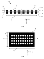
- Fig. 2A shows a prior art electrode assembly (1a ') in cross-section, while Fig. 2B shows a grid electrode in plan view.
- the line AA in Fig. 2B marks the section line of the representation of Fig. 2A .
- the prior art electrode assembly (1a ') comprises a plasma grid electrode (11'), a gridded grid electrode (12 '), an accelerator grid electrode (13') and a ground grid electrode (14 ').
- Each of these grid electrodes consists of an electrically conductive grid electrode material (15) and has openings (16) through which the extracted electrical charge carriers, hereinafter called particles for short, can pass in the z-direction.
- the z-direction is thus the particle exit direction. That is, the openings (16) extend from one surface of the grid electrode to the opposite surface of the grid electrode, wherein the opening may be straight or oblique. Metals, for example molybdenum or tungsten, or graphites are used as the grid electrode material, wherein the grid electrode material may also be a layer sequence of a plurality of electrically conductive materials or also of an electrically non-conductive base body with a coating of an electrically conductive material.
- the openings (16) can have different peripheral geometries, for example they can be round, elliptical or polygonal, have different dimensions and / or be distributed uniformly or non-uniformly over the lateral extent of the grid electrode in the xy plane.
- the openings (16) have, for example, a hole diameter of 0.5 mm to 3 mm, while the grid electrode material (15) typically has a land width, ie a width between two adjacent openings (16) of 0.5 mm to 1 mm.
- the distribution of the openings (16) over the entire lateral extent of a grid electrode can be configured such that a homogeneous distribution of the current density in the particle beam or in selected areas of the particle beam is achieved.
- the achievable current density can be adjusted in a corresponding area of the particle beam.
- a high current density is achieved by a dense arrangement of openings (16), ie small web widths.
- Each grid electrode has a first lateral extent (10) in the x-direction, a second lateral extent (19) in the y-direction and a thickness (17) in the z-direction, wherein the first lateral extent (10) and the second lateral extent (19) may be from a few mm to a few meters and the thickness (17) may typically be 200 ⁇ m to 1 mm.
- the grid electrodes can have any desired peripheral geometry, which can be, for example, rectangular, round, elliptical or polygonal.
- all grid electrodes of an electrode arrangement have the same design or only slight differences in the parameters mentioned.
- the individual grid electrodes have a distance (18) from one another, which is typically between 0.5 mm and 1.5 mm and is preferably the same between all grid electrodes.
- the mentioned grid electrode parameters are chosen according to the mechanical, electrical and thermal loading of the grid electrodes.
- the grid electrodes are each formed in a layer which is either flat, as in the Fig. 2A shown, or has a radius of curvature, but the distance between the individual grid electrodes always remains approximately the same. It is characteristic that each grid electrode is formed only in one layer and each layer is completely electrically isolated from the other layers.
- an inventive electrode arrangement (1a), as shown in Fig. 3 is characterized by an electrically conductive connection between a grid electrode area forming a layer portion of a first layer and a grid electrode area formed in a second layer, the grid electrode area in the first layer being electrically insulated from other grid electrode areas in the first layer is.
- Fig. 3 shows a schematic representation of this arrangement. There are shown a first layer (100) and a second layer (200), which are symbolized by dashed lines and each form a closed surface. The first layer (100) and the second layer (200) are spaced apart by a first distance (300). In the first layer (100), a first grid electrode is arranged, which has first grid electrode areas (110a, 110b).
- These grid electrode regions (110a, 110b) form the first layer portion (101) of the first layer (100).
- a second grid electrode is arranged, which has first grid electrode areas (210a, 210b).
- a further grid electrode region is arranged which forms a second layer portion (102) of the first layer (100) and which is electrically insulated from the first layer portion (101) of the first layer (100). but electrically conductively connected to the first grid electrode regions (210a, 210b) of the second grid electrode in the second layer (200).
- This electrical connection is shown schematically by the lines with the reference numeral 301, wherein the electrical connection (301) no electrical line in the sense of a wire bridge o.ä. have to be.
- the second layer portion (102) may be spaced from the circumference of the first layer (100), ie, located within the first layer (100). Nevertheless, via the electrical connection (301) with the first grid electrode regions (210a, 210b) of the second grid electrode, which adjoin the circumference of the second layer (200), an impact of the second layer portion (102) with an electric potential, that of the electric Potential of the first layer portion (101) is different, via an electrical contact to the outer boundary, ie the circumference, the electrode assembly (1 a) possible.
- first grid electrode regions (210a, 210b) of the second grid electrode in addition to the first grid electrode regions (210a, 210b) of the second grid electrode, further grid electrode regions of the second grid electrode or grid electrode regions of a further grid electrode may be formed. It is also possible for the first grid electrode regions (210a, 210b) of the second grid electrode to extend continuously over the entire second layer (200). For a clear presentation of the basic idea according to the invention are in Fig. 3 only the first grid electrode regions (210a, 210b) of the second grid electrode have been shown while other regions in the second layer (200) have been omitted.
- the configuration of the electrical connection (301) and the first grid electrode and the second grid electrode will be explained below with reference to some embodiments, wherein the representation of the openings (16) in the individual grid electrodes is omitted for clarity. Also, only one grid electrode area forming the second layer portion is shown, and the number of these grid electrode areas is not limited.
- the first grid electrode has only the first grid electrode areas (110a, 110b) and thus does not cover the entire first layer (100), while the second layer section (102) of the first layer (100) is formed by a second grid electrode region (210c) of the second grid electrode.
- Fig. 4 shows a first embodiment of this embodiment, wherein the second grid electrode region (210c) is thicker than the first grid electrode regions (210a, 210b) of the second grid electrode.
- a first surface (211) of the second grid electrode region (210c) is formed in the first layer (100)
- a second surface (212) of the second grid electrode region (210c) is disposed in the second layer (200).
- the first surface (211) and the second surface (212) face each other.
- the second grid electrode "protrudes" into the first layer (100).
- the second grid electrode area (210c) is preferably integral with the first one Grid electrode regions (210a, 210b) of the second grid electrode formed and can be prepared, for example, by means of an additive (selective deposition) or a subtractive (etching) method.
- the geometry of the openings, for example the hole diameter, in the second grid electrode area (210c) is changed relative to that of the openings in the first grid electrode areas (210a, 210b) in order to compensate for the effects of the greater thickness of this area on the passing charge carriers.
- the openings in the second grid electrode area (210c) may also be arranged differently than in the first grid electrode areas (210a, 210b).
- Fig. 5 11 shows a second embodiment of the first embodiment in which the second grid electrode region 210c has the same thickness as the first grid electrode regions 210a, 210b of the second grid electrode and is formed integrally therewith.
- This embodiment can be produced, for example, by a forming process of the second grid electrode, such as swaging. Again, the geometry and / or arrangement of the openings in the second grid electrode area (210c) may differ from that in the first grid electrode areas (210a, 210b).
- the transitions between the first grid electrode areas (210a, 210b) and the second grid electrode area (210c) may be continuous. This is exemplary of the first embodiment in FIG Fig. 6 shown. In this case, the transition between the first surface (211) of the second grid electrode area (210c) to the surface of the first grid electrode areas (210a, 210b) in each case runs obliquely. Alternatively or additionally, the surfaces of the second grid electrode may be rounded at the transition points, so that a round "edge" is formed.
- Fig. 7 shows a further embodiment of the first embodiment, wherein the second grid electrode region (210c) of the second grid electrode is not formed integrally with the first grid electrode region (210a) of the second grid electrode.
- the first grid electrode region (210a) completely covers the second layer (200), while the second grid electrode region (210c) is spaced from the first grid electrode region (210a) of the second grid electrode by the first distance (300) and via at least one electrically conductive spacer (210). 302) is connected to the first grid electrode area (210a) of the second grid electrode.
- Such spacers (302) may be, for example, bumps, balls, cylinders, or the like, which include both the electrical connection and ensure the mechanical stability of the arrangement of the second grid electrode region (210c) in the first layer (100).
- the second grid electrode area (210c) of the second grid electrode has no physical (mechanical) connection to the first grid electrode areas (110a, 110b) of the first grid electrode except via the spacers (302).
- the second grid electrode region (210c) may be formed as a self-contained device, which is subsequently connected to the first grid electrode region (210a) by means of the spacers (302).
- the second grid electrode area (210c) common to the first grid electrode area (210a) of the second grid electrode or to the first grid electrode areas (110a, 110b) of the first grid electrode, and later to generate a physical / mechanical "separation" ,
- the first grid electrode has, in addition to the first grid electrode areas (110a, 110b), a second grid electrode area (110c) which is physically (mechanically) connected to the first grid electrode areas (110a, 110b) and the second grid electrode Layer portion (102) of the first layer (100) forms.
- the first grid electrode forms the entire first layer (100). This is in Fig. 8 shown.
- the second grid electrode region (110c) of the first grid electrode is electrically insulated from the first grid electrode regions (110a, 110b) by electrically insulating grid electrode regions (110d) and is electrically conductive with the first grid electrode region (210a) of the second grid electrode, completely covering the second layer (200) fills, connected via at least one electrically conductive connection (301).
- electrically conductive connections (301) can again be used with reference to Fig. 7 be described spacer, but in this embodiment does not have to ensure the mechanical stability of the arrangement, as this is already given by the electrically insulating grid electrode regions (110d) of the first grid electrode.
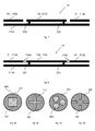
- the second layer portion (102) can be formed by a coherent grid electrode area. This is in the Figs. 9A and 9B which shows the first layer (100) with the first layer portion (101) and the second layer portion (102). The electrical insulation by a physical distance or an electrically insulating intermediate region between the two ply shares is not shown here.
- Figs. 9C and 9D show other embodiments in which the second layer portion (102) is formed by a plurality of spaced apart grid electrode regions.
- three round grid electrode areas form the second layer portion (102) while in Fig. 9D four rectangular grid electrode areas form the second layer portion (102).
- the grid electrode areas of the second layer portion (102) are each of which is uniformly formed with respect to its circumferential geometry and arranged uniformly within the first layer (100), for example, with respect to a center of the first layer (100).
- the individual grid electrode areas can also be designed differently with respect to their circumferential geometry and / or their arrangement within the first layer (100).
- the grid electrode regions which form the second layer portion (102) can also adjoin the circumference of the first layer (100).
- the circumferential geometry of the first layer (100) and the grid electrode regions forming the second layer portion (102) is not limited to the geometries shown. Also, another arrangement of the grid electrode regions forming the second layer portion (102) within the first layer (100) is possible.
- the peripheral geometries and dimensions of the grid electrode regions forming the second layer portion (102) and their arrangement within the first layer (100) represent a pattern of the electrode assembly (1a).
- the electrode arrangement may also have further grid electrodes, which are likewise electrically conductive and have corresponding openings.
- the electrode arrangement (1a) consists of four grid electrodes.
- these are the first grid electrode (110) which implements a grid element (12), the second grid electrode (210), which constitutes an acceleration grid electrode (13), and two further grid electrodes (401, 402), which serve as the plasma grid electrode (11 ) and ground grid electrode (14).
- the grid electrodes may also be arranged differently, in which case the functionalities of the grid electrodes are also different.
- the first grid electrode (110) is the grid electrode and the plasma grid electrode realizes the second grid electrode (210).
- the grid electrodes in the particle exit direction, ie away from the charge generation space are always arranged in the following order: plasma grid electrode (11), grid electrode (12), acceleration grid electrode (13), and ground grid electrode (14).
- further grid electrodes may, for example, be arranged between the plasma grid electrode (11) and the switch grid electrode (12) or between the acceleration grid electrode (13) and the ground grid electrode (14), but not between the grid electrodes which form the first grid electrode and the second grid electrode.
- the further grid electrodes (401, 402) each comprise at least one first grid electrode area, which is arranged in a further layer, wherein the further layer and the layer adjacent to it are spaced from each other by a further distance along the particle exit direction.
- the plasma grid electrode 11 is arranged in a third position, which is spaced apart from the first position by a second distance, wherein the plasma grid electrode 11 has only grid electrode regions in the third position in the illustrated case.
- the plasma grid electrode (11) is uniform and has no "bulges" or other irregularities that may, for example, affect a plasma unfavorable.
- the acceleration grid electrode (13), according to the second embodiment of the first embodiment of the electrode assembly (1a), as in Fig. 5 is shown, configured and thus “invaded” into the first layer, one (or more) of the further grid electrodes, which is arranged on the side facing away from the first grid electrode (110) side of the second grid electrode (210), second grid electrode regions which are arranged in the second layer.
- further grid electrodes can be inserted into the respective adjacent layer.
- the ground grid electrode (14) having first grid electrode areas (402a, 402b) and a second grid electrode area (402c).
- the first grid electrode regions (402a, 402b) are disposed in a fourth layer spaced at a third distance from the second layer, while the second grid electrode region (402c) is disposed in the second layer.
- the distances between regions with different potential for example between the acceleration grid electrode (13) and the ground grid electrode (14), over the entire extent of the respective grid electrodes across, so that a uniform particle beam is formed.
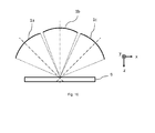
- Fig. 11 shows an example of an electrode assembly (1a) in which the individual layers are not flat, but curved surfaces, so that the individual, partially sub-beams (8) passing through the openings in the grid electrodes are focused so that they all in a common incident surface concentrated impact on a substrate (9).
- the electrode assembly (1a) again with reference to Fig. 10 described grid electrodes, wherein the first grid electrode (110) and the second grid electrode (210) as in the reference to the Fig. 5 described embodiment are formed.
- An adaptation of the peripheral geometries, the dimensions and / or the arrangement of the openings in the individual grid electrodes is advantageous in order to compensate for the configuration of the layers as curved surfaces, ie as surfaces with an impressed, finite radius.
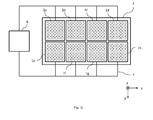
- FIG. 12 an embodiment of the inventive device (1) for the extraction of charge carriers with a plurality of electrode assemblies (1a - 1h) is shown in plan view.
- the electrode arrangements (1a-1h) are arranged in a 4x2 matrix, ie, two electrode arrangements (1a-1d or 1e-1h) are arranged in two rows.
- a first lateral extent of the device (1) ie along the x-direction
- four electrode arrangements (1a-1d or 1e-1h) are arranged side by side
- a second lateral extent of the device (1) ie along the y direction, only two electrode arrangements are arranged side by side.
- all the electrode assemblies (1a-1h) are electrically contactable from the outer periphery of the device (1), so that they are acted upon by the switching device (6) or a plurality of switching devices and the corresponding electrical lines (7) with one or more electrical potentials can.
- all the electrode assemblies (1a-1h) have the same pattern of the layer portions of the first layer, but one or more or all of the electrode arrangements may also have different patterns.
- the electrode arrangements (1a-1h) cover almost the entire lateral extent of the device (1), wherein only edge areas and intermediate areas between the individual electrode arrangements (1a-1h) are not covered.
- the inventive device (1) is operated, so that a desired beam characteristic of at least one electrode assembly (1a) passing through particle beam is generated.
- the wiring of an electrode arrangement is shown, which has a switching grid electrode (12), which acts as a first grid electrode (110), and an acceleration grid electrode (13), which acts as a second grid electrode (210), wherein the acceleration grid electrode (13) in Particle exit direction after the switch grid electrode (12) is arranged.
- the first grid electrode (110) and the second grid electrode (210) are, for example, as in FIG Fig. 4 illustrated first embodiment of the first embodiment.
- the first grid electrode (110) and the second grid electrode (210) are connected via a switching device (6) to an apparatus (5) for generating electrical voltages which have at least two different values for a first potential of the first grid electrode areas (110a, 110b).
- the first grid electrode (110) and at least two different values for a second potential of the first grid electrode areas (210a, 210b) of the second grid electrode (210) and of the second grid electrode area (210c) of the second grid electrode (210) which is electrically conductively connected thereto.
- the first potential has a first value U 11 and the second potential has a second value U 21 , the values being suitable for extracting charge carriers from the charge generation space. That is, the first value U 11 and the second value U 21 are smaller (more negative) for positive carriers than the value of the potential in the carrier generation space or the potential of a plasma grid electrode (hereinafter called U beam ), while it is reversed for negative carriers.
- the amount of the second value U 21 may, for example, deviate by a maximum of ⁇ 10% from the value of the first value U 11 .
- even larger differences are possible as long as the first and second potential allow the passage of charge carriers through all grid electrode areas.
- the entire lateral extent of the electrode assembly used for the extraction of charge carriers is both suitable for extracting carriers
- the entire lateral extent of the electrode assembly used for the extraction of charge carriers is both suitable for extracting carriers
- the entire lateral extent of the electrode assembly used for the extraction of charge carriers is both suitable for extracting carriers
- the entire lateral extent of the electrode assembly used for the extraction of charge carriers is both suitable for extracting carriers
- the entire lateral extent of the electrode assembly used for the extraction of charge carriers is both suitable for extracting carriers
- such an focused ion beam for an exemplary electrode arrangement having a grid electrode diameter of 40 mm can have an impact diameter on a substrate surface of about 4.5 mm to be processed.
- grating electrode diameter is understood to mean the diameter of a circular region of the electrode arrangement relative to a layer in which grating electrode regions are formed.
- the grid electrode areas have the openings described above, while the individual grid electrodes can also have edge areas, for example for physically fixing the grid electrode in a housing or another device or for applying a potential to the grid electrode, in which no openings are formed.
- edge areas for example for physically fixing the grid electrode in a housing or another device or for applying a potential to the grid electrode, in which no openings are formed.
- the first potential has a third value U 12
- the second potential has a fourth value U22.
- the third value U 12 is suitable for preventing or greatly restricting the extraction of charge carriers from the charge carrier generation space.
- the third value U 12 is larger (more positive) than the value of the potential in the carrier generation space or as U beam , while it is reversed for negative carriers.
- the fourth value U 22 is suitable for extracting charge carriers, wherein the fourth value U 22 may be equal to the second value U 21 , as shown in FIG Fig. 13B is shown.
- the fourth value U 22 may also be different from the second value U 21 in order to compensate for the changed electrical environmental conditions.
- the second grid electrode region (210c) of the second grid electrode (210) which forms the second layer portion of the first layer and is electrically conductively connected to the first grid electrode regions (210a, 210b) of the second grid electrode (210)
- the sub-beam (20b) only images the geometry of the second layer portions of the first layer and has dimensions smaller than that of the overall beam (20a).
- a partial beam (20b) having a smaller diameter of, for example, approximately 2 mm is thus produced, the diameter of the second grid region (210c) of the second grid electrode (210), ie the diameter of the second layer portion of the first layer, 10 mm.
- the first potential has a fifth value U 13 and the second potential has a sixth value U 23 , wherein the fifth value U 13 and the sixth value U 23 are suitable for preventing or severely restricting the extraction of charge carriers from the charge carrier generation space.
- the fifth value U 13 and the sixth value U 23 are thus greater (more positive) for positive charge carriers than the value of the potential in the charge carrier generation space or as U beam , while it is reversed for negative charge carriers.
- the fifth value U 13 may be equal to the third value U 12 , as in Fig. 13C is shown. However, the fifth value U 13 may also be different from the third value U 12 to compensate for the changed electrical environmental conditions.
- the sixth value can be U 23 equal to or almost equal to or different from the fifth value U. 13 Since now all the layer portions of the first layer are at a potential that prevents the extraction of charge carriers, no particle beam is generated.
- the following table shows example values for the potential of a plasma grating as well as for passing or blocking values of the first and second potentials for positive charge carriers: U beam U 11 U 12 , U 13 U 21 , U 22 U 23 700V -100 V 800 ... 900V -100 V 800 ... 900V
- a particle beam which extends over the entire lateral extent of the electrode arrangement but has a different particle density or particle energy in the region of the first layer portion than in the region of the second can thus also be produced Location share.
- the first and / or the second potential can also be acted pulsed, wherein the pulse duration and the pulse ratio may be the same or different from each other and / or over time.
- the plasma lattice can be acted upon or floated as illustrated above with a third potential U beam .
- the electrode assembly after the accelerating grid further comprises a ground grid electrode, then this is preferably grounded.
- a particle beam source (3) which comprises the device (1) according to the invention for the extraction of electrical charge carriers and generates a particle beam (20) which strikes and processes the surface of a substrate (9).
- the particle beam source (3) and the substrate surface with a distance (21) along the z-direction, ie the particle exit direction, arranged by a movement of the particle beam source (3) and / or the substrate (9) along the z-direction is changeable.
- the particle beam source (3) and / or the substrate (9) can be moved laterally, ie in the x and / or y direction, tilted to the z direction and / or to the xy plane and / or about an axis, which is parallel to the z-direction, to be rotated. All movements can be performed uniformly or non-uniformly.
- the beam characteristic of the particle beam (20) in dependence on a known property pattern of the substrate surface and the process progress is thus determined with the aid of the above-described method for controlling the beam characteristic ( Figs. 13A to 13C ) is controlled so that after completion of the processing, a desired property pattern of the substrate surface is present. For example.
- the substrate surface in large areas with a homogeneous property pattern with a particle beam with a large lateral extent, for example.
- the total beam (20a) Fig. 13A processed
- a particle beam having a smaller lateral extent for example, the sub-beam (20b) Fig. 13B .
- the desired processing quality or quantity in a particular area of the substrate surface may be critical to the selection of a particular beam characteristic.
- a plurality of particle beams from one or more apparatuses according to the invention (1) are used for the extraction of electrical charge carriers for processing the substrate surface, then the substrate surface can be processed simultaneously in a plurality of lateral areas of the substrate surface.
- Fig. 15 3 wherein by way of example three electrode arrangements (1a-1c) of an apparatus (1) for the extraction of electrical charge carriers are shown.
- the electrode assemblies (1a-1c) may be included in each one of a plurality of electric charge carrier extraction devices (1), and a specific electric charge carrier extraction device (1) is contained in a specific particle beam source, respectively.
- identical or different methods that use different particles or different beam characteristics for processing can be performed simultaneously.
- FIG. 16 A further embodiment of the method for processing a substrate surface is shown, in which the particle beams generated by means of the electrode arrangements (1a-1c) impinge on one or more devices (1) for the extraction of electrical charge carriers on a common surface on the substrate surface. That is, the particle beams are aligned on one and the same surface area, the common area being determined by the incident surface of the particle beam with the greatest lateral extent in the plane of the substrate surface.
- the different particle beams have different lateral dimensions and may have different shapes, foci, particle densities, particle energies and / or particle types.
- structures in the substrate surface can be created, which have different etching depths, in which, for example, a particle beam with a small lateral extent and a particle beam with a large lateral extent are combined.
- etching depths in which, for example, a particle beam with a small lateral extent and a particle beam with a large lateral extent are combined.
- All configurations and embodiments of the device (1) according to the invention for the extraction of electrical charge carriers and the method for operating the inventive device (1) for the extraction of electrical charge carriers and for processing a substrate surface can be combined with each other and with each other, as long as this is not explicitly excluded or is impossible for physical and / or technical reasons.
Landscapes
- Chemical & Material Sciences (AREA)
- Physics & Mathematics (AREA)
- Optics & Photonics (AREA)
- Engineering & Computer Science (AREA)
- Combustion & Propulsion (AREA)
- Analytical Chemistry (AREA)
- Electron Sources, Ion Sources (AREA)
- Junction Field-Effect Transistors (AREA)
- Apparatus Associated With Microorganisms And Enzymes (AREA)
Abstract
Die Erfindung betrifft eine Vorrichtung zur Extraktion von elektrischen Ladungsträgern aus einem Ladungsträgererzeugungsraum mit mindestens einer Elektrodenanordnung 1a zur Extraktion von Ladungsträgern, wobei die mindestens eine Elektrodenanordnung mindestens eine erste Gitterelektrode und eine zweite Gitterelektrode mit korrespondierenden Öffnungen aufweist. Die erste und die zweite Gitterelektrode enthalten jeweils mindestens einen ersten elektrisch leitfähigen Gitterelektrodenbereich 110,210, wobei der mindestens eine erste Gitterelektrodenbereich 110a,b der ersten Gitterelektrode in einer ersten Lage 100 und der mindestens eine erste Gitterelektrodenbereich 210a,b der zweiten Gitterelektrode in einer zweiten Lage 200 ausgebildet sind. Die erste Lage und die zweite Lage sind innerhalb der Elektrodenanordnung in Teilchenaustrittsrichtung nacheinander angeordnet und voneinander durch einen ersten Abstand 300 entlang der Teilchenaustrittsrichtung beabstandet, wobei der mindestens eine erste Gitterelektrodenbereich 110a, b der ersten Gitterelektrode in der ersten Lage einen ersten elektrisch leitfähigen Lagenanteil 101 bildet. Darüber hinaus ist in der ersten Lage ein zweiter elektrisch leitfähiger Lagenanteil 102 ausgebildet, der elektrisch vom ersten Lagenanteil 101 isoliert ist. Der zweite Lagenanteil 102 wird durch mindestens einen zweiten elektrisch leitfähigen Gitterelektrodenbereich der ersten Gitterelektrode oder der zweiten Gitterelektrode gebildet und der zweite Lagenanteil 102 ist elektrisch leitend 301 mit dem mindestens einen ersten Gitterelektrodenbereich 210a,b der zweiten Gitterelektrode verbunden. Die erfindungsgemäße Vorrichtung zur Extraktion von Ladungsträgern stellt somit eine elektrisch schaltbare Extraktionsgitterelektrodenanordnung dar, mit deren Hilfe die Strahlcharakteristik eines Teilchenstrahls aus extrahierten Ladungsträgern verändert werden kann.The invention relates to a device for the extraction of electrical charge carriers from a charge carrier generation space having at least one electrode arrangement 1a for the extraction of charge carriers, wherein the at least one electrode arrangement has at least one first grid electrode and one second grid electrode with corresponding openings. The first and the second grid electrodes each contain at least one first electrically conductive grid electrode area 110, 210, the at least one first grid electrode area 110 a, b of the first grid electrode in a first position 100 and the at least one first grid electrode area 210 a, b of the second grid electrode in a second position 200 are formed. The first layer and the second layer are arranged one after the other within the electrode arrangement in the particle exit direction and spaced from each other by a first distance 300 along the particle exit direction, the at least one first grid electrode region 110a, b of the first grid electrode forming a first electrically conductive layer portion 101 in the first layer , In addition, a second electrically conductive layer portion 102 is formed in the first layer, which is electrically isolated from the first layer portion 101. The second layer portion 102 is formed by at least one second electrically conductive grid electrode region of the first grid electrode or the second grid electrode, and the second layer portion 102 is electrically conductively connected to the at least one first grid electrode region 210a, b of the second grid electrode. The device according to the invention for the extraction of charge carriers thus represents an electrically switchable extraction grid electrode arrangement with the aid of which the beam characteristic of a particle beam of extracted charge carriers can be changed.
Description
Die Erfindung betrifft eine Vorrichtung zur Extraktion von elektrischen Ladungsträgern aus einem Ladungsträgererzeugungsraum, die eine Änderung der Form des mit Hilfe der Vorrichtung extrahierten Teilchengesamtstrahls ermöglicht, sowie ein Verfahren zum Betreiben einer solchen Vorrichtung. Darüber hinaus betrifft die Erfindung ein Verfahren zum Bearbeiten der Oberfläche eines Substrates unter Nutzung eines oder mehrerer Teilchengesamtstrahlen, die mit mindestens einer derartigen Vorrichtung erzeugt wurden.The invention relates to a device for the extraction of electrical charge carriers from a charge carrier generation space, which allows a change in the shape of the total particle beam extracted by means of the device, and a method for operating such a device. Moreover, the invention relates to a method of processing the surface of a substrate using one or more total particle beams generated by at least one such device.
Gerichtete Teilchenstrahlen aus elektrischen Ladungsträgern, bspw. Ionenstrahlen oder Elektronenstrahlen, werden in einer Teilchenstrahlquelle durch die Extraktion von elektrischen Ladungsträgern, also Ionen oder Elektronen, aus einem Ladungsträgererzeugungsraum, bspw. einem Plasma, erzeugt, wobei die Teilchen sich nach Verlassen der Teilchenstrahlquelle gerichtet und strahlförmig im Raum in eine Teilchenaustrittsrichtung bewegen. Dazu werden, insbesondere zur Erzeugung von Breitstrahlen mit einer Strahlbreite von bis zu 1 m, eine oder mehrere Vorrichtung zur Extraktion von elektrischen Ladungsträgern eingesetzt, die jeweils aus einer oder mehreren Gitterelektroden bestehen und die Teilchen aus dem Ladungsträgererzeugungsraum extrahieren und ggf. beschleunigen sowie die dabei entstehenden einzelnen Teilchenteilstrahlen zueinander ausrichten. Unter einer Gitterelektrode wird dabei ein mechanischer (physischer oder materieller) Verbund einer Mehrzahl, d.h. von mindestens zwei, von Öffnungen, durch die die Ladungsträger hindurchtreten können, verstanden. Mit anderen Worten: Eine Gitterelektrode ist ein (im Allgemeinen) flächenförmiges Bauteil, dessen lateralen Abmessungen um ein Vielfaches größer als seine Dicke, d.h. seine Ausdehnung in Teilchenaustrittsrichtung, sind und das eine Vielzahl von Öffnungen aufweist, die sich in Dickenrichtung über die gesamte Dicke des Bauteils erstrecken und einen Durchtritt von Ladungsträgern durch das Bauteil ermöglichen. Die Gitterelektrode weist zumindest in einigen Bereichen ein elektrisch leitfähiges Material auf, das mit einem Potential beaufschlagt werden kann, so dass die Ladungsträger extrahiert und beschleunigt oder der oder die Teilstrahlen gesperrt werden können. Die elektrisch leitfähigen Gitterelektrodenbereiche können physisch und elektrisch leitend miteinander verbunden sein. Dies ist bspw. bei einer vollständig aus einem elektrisch leitfähigen Material ausgebildeten Gitterelektrode der Fall. Jedoch können die einzelnen elektrisch leitfähigen Gitterelektrodenbereiche auch elektrisch voneinander isoliert sein, bspw. durch ein dazwischen angeordnetes elektrisch isolierendes Material. In einer Vorrichtung zur Extraktion von elektrischen Ladungsträgern können mehrere Gitterelektroden in Teilchenaustrittsrichtung nacheinander in voneinander beabstandeten Lagen angeordnet werden, wobei die Öffnungen der einzelnen Gitterelektroden zueinander korrespondieren, so dass bei einer entsprechenden Potentialbeaufschlagung der einzelnen Gitterelektroden oder Gitterelektrodenbereiche Ladungsträger als Teilchenteilstrahlen durch die Öffnungen der Gitterelektroden hindurchtreten können. Oftmals werden mindestens drei Gitterelektroden eingesetzt, die als Plasma-, Screen- oder Beamgitterelektrode, als Beschleunigungs- oder Accelerationsgitterelektrode und als Massegitterelektrode entsprechend ihrer Funktion bezeichnet werden. Jedoch können auch weitere Elektroden in der Vorrichtung zur Extraktion von elektrischen Ladungsträgern angeordnet werden, um bspw. den erzeugten Teilchengesamtstrahl bezüglich seiner Austrittsrichtung zu beeinflussen.Directed particle beams from electrical charge carriers, for example ion beams or electron beams, are generated in a particle beam source by the extraction of electrical charge carriers, ie ions or electrons, from a charge carrier generation space, for example a plasma, whereby the particles are directed and jet-shaped after leaving the particle beam source move in space in a particle exit direction. For this purpose, in particular for the production of broad beams with a beam width of up to 1 m, one or more apparatus for the extraction of electrical charge carriers used, each consisting of one or more grid electrodes and extract the particles from the charge carrier generation space and possibly accelerate and the case Align the resulting individual particle beams to each other. In this case, a grating electrode is understood to be a mechanical (physical or material) composite of a plurality, ie of at least two, of openings through which the charge carriers can pass. In other words, a grid electrode is a (generally) sheet-like component whose lateral dimensions are many times greater than its thickness, ie its extension in the particle exit direction, and which has a plurality of openings extending in the thickness direction over the entire thickness of the Extend component and allow passage of charge carriers through the component. At least in some areas, the grid electrode has an electrically conductive material that can be acted on by a potential so that the charge carriers can be extracted and accelerated or the partial beam or beams can be blocked. The electrically conductive grid electrode regions may be physically and electrically conductively connected to each other. This is the case, for example, with a grid electrode formed entirely from an electrically conductive material. However, the individual electrically conductive grid electrode regions may also be electrically insulated from one another, for example by an electrically insulating material arranged therebetween. In a Apparatus for extracting electrical charge carriers, a plurality of grid electrodes in the particle exit direction can be successively arranged in spaced-apart layers, wherein the openings of the individual grid electrodes correspond to each other, so that with a corresponding potential application of the individual grid electrodes or grid electrode areas charge carriers can pass as particle partial beams through the openings of the grid electrodes. Often, at least three grid electrodes are used, which are referred to as a plasma, screen or beam grid electrode, as an acceleration or accelerating grid electrode and as a ground grid electrode according to their function. However, other electrodes can also be arranged in the device for the extraction of electrical charge carriers in order, for example, to influence the generated total particle beam with respect to its exit direction.
Teilchenstrahlen werden bspw. in lonenstrahl- oder Elektronenstrahlbearbeitungsanlagen unter anderem zur Bearbeitung von Oberflächen eines Substrates eingesetzt. Dabei können die Topographie der Oberfläche oder andere physikalische oder chemische Eigenschaften der Oberfläche, wie bspw. hygroskopische Eigenschaften, durch das Auftreffen der Teilchen auf der Oberfläche verändert werden. Dabei hängen sowohl die erreichbare Auflösung, also die minimale bearbeitete Fläche, als auch die Qualität der Bearbeitung stark von der Strahlbreite des eingesetzten Gesamtstrahls ab. Im Allgemeinen gilt dabei, dass mit einer kleinen Strahlbreite bessere Bearbeitungsergebnisse erzielt werden. Beispielsweise können kleine Dickenunterschiede innerhalb einer auf der Oberfläche des Substrats befindlichen Schicht genauer mit einem Gesamtstrahl mit einer kleinen Strahlbreite eingeebnet werden als mit einem Gesamtstrahl mit einer großen Strahlbreite. Dem steht jedoch eine längere Bearbeitungsdauer eines Substrates mit einer gegebenen Fläche gegenüber.Particle beams are used, for example, in ion beam or electron beam machining systems, inter alia for processing surfaces of a substrate. The topography of the surface or other physical or chemical properties of the surface, such as, for example, hygroscopic properties, can be changed by the impact of the particles on the surface. Both the achievable resolution, ie the minimum machined surface, and the quality of the processing depend strongly on the beam width of the total beam used. In general, better results are achieved with a small beam width. For example, small differences in thickness within a layer located on the surface of the substrate can be more accurately leveled with a total beam having a small beam width than with an overall beam having a large beam width. However, this is offset by a longer processing time of a substrate with a given area.
Zur Lösung dieses Problems sind aus dem Stand der Technik verschiedene Möglichkeiten zur Formung eines lonenstrahls bekannt, bei denen die Breite oder Form des lonenstrahls an die notwendige Bearbeitungsqualität oder Bearbeitungsauflösung angepasst werden kann. Dies umfasst zum Einen die Nutzung verschiedener Blenden oder Gitterelektrodenanordnungen, mit denen ein Teil des lonenstrahls ausgeblendet werden kann bzw. erst gar nicht extrahiert wird. Zur Anpassung der Breite des lonenstrahls werden dann die Blende oder das bzw. die Gitter oder eventuell auch die gesamte Ionenstrahlquelle gewechselt, was jedoch zu Verunreinigungen durch die mechanische Bewegung führt oder lange Einlaufzeiten der neu installierten Ionenstrahlquelle nach sich zieht.To solve this problem, various possibilities for shaping an ion beam are known from the prior art, in which the width or shape of the ion beam can be adapted to the necessary processing quality or processing resolution. On the one hand, this includes the use of different diaphragms or grid electrode arrangements with which a part of the ion beam can be masked out or not even extracted at all. To adjust the width of the ion beam then the aperture or the or the grid or possibly the entire ion beam source are changed, but this leads to contamination by the mechanical movement or pulls long run-in times of the newly installed ion beam source by itself.
Des Weiteren ist die gezielte elektrische Steuerung einzelner lateraler Bereiche der Gitterelektrodenanordnung bekannt. So wird bspw. in der
Nachteilig an diesen Vorrichtungen ist, dass elektrische Leitungen aus dem Inneren einer Gitterelektrode nach außen zu einer Spannungsversorgung geführt werden müssen. Bei den vorhandenen Potentialunterschieden von bis zu 1500 V zwischen den verschiedenen Gitterelektroden oder Gitterelektrodenbereichen sowie Temperaturen von bis zu 300°C, denen die Gitterelektroden während des Betriebs der Teilchenstrahlquelle ausgesetzt sind, stellt diese Art der Potentialbeaufschlagung eine große Herausforderung dar.A disadvantage of these devices is that electrical lines from the interior of a grid electrode must be led to the outside to a power supply. Given the potential differences of up to 1500 V between the various grid electrodes or grid electrode areas and temperatures of up to 300 ° C, to which the grid electrodes are exposed during the operation of the particle beam source, this type of potential application poses a great challenge.
Aus der
Es ist daher Aufgabe der vorliegenden Erfindung, die Nachteile des Standes der Technik zu überwinden und eine einfache Möglichkeit zur Formung eines Teilchengesamtstrahls mit Hilfe von elektrisch schaltbaren Gitterelektroden bereitzustellen.It is therefore an object of the present invention to overcome the disadvantages of the prior art and to provide a simple way of forming a total particle beam by means of electrically switchable grid electrodes.
Diese Aufgabe wird durch die Vorrichtung zur Extraktion von elektrischen Ladungsträgern und das Verfahren zum Betreiben der Vorrichtung zur Extraktion von elektrischen Ladungsträgern gemäß den unabhängigen Ansprüchen gelöst. Darüber hinaus wird ein Verfahren zur Bearbeitung einer Oberfläche eines Substrates unter Nutzung einer solchen Vorrichtung zur Extraktion von elektrischen Ladungsträgern beansprucht. Vorteilhafte Weiterbildungen finden sich in den Unteransprüchen.This object is achieved by the device for the extraction of electrical charge carriers and the method for operating the device for the extraction of electrical charge carriers according to the independent claims. In addition, a method for processing a surface of a substrate using such a device for the extraction of electrical charge carriers is claimed. Advantageous developments can be found in the subclaims.
Eine erfindungsgemäße Vorrichtung zur Extraktion von elektrischen Ladungsträgern aus einem Ladungsträgererzeugungsraum umfasst mindestens eine Elektrodenanordnung, die mindestens eine erste Gitterelektrode und eine zweite Gitterelektrode mit korrespondierenden Öffnungen aufweist, die jeweils mindestens einen ersten Gitterelektrodenbereich enthalten, der elektrisch leitfähig ausgebildet ist. Die Öffnungen dienen dem Durchtritt der Ladungsträger durch die jeweilige Gitterelektrode in Teilchenaustrittsrichtung und weisen laterale Ausdehnungen und eine vorgegebene Umfangsgeometrie, bspw. eine runde, elliptische, eckige oder unregelmäßige Umfangsgeometrie, auf. Dabei können die lateralen Ausdehnungen und/oder die Umfangsgeometrien von zueinander korrespondierenden Öffnungen in der ersten und der zweiten Gitterelektrode geringfügig voneinander abweichen.A device according to the invention for the extraction of electrical charge carriers from a charge carrier generation space comprises at least one electrode arrangement which has at least one first grid electrode and one second grid electrode with corresponding openings each having at least a first grid electrode region, which is formed electrically conductive. The openings serve for the passage of the charge carriers through the respective grid electrode in the particle exit direction and have lateral expansions and a predetermined circumferential geometry, for example a round, elliptical, angular or irregular circumferential geometry. In this case, the lateral expansions and / or the circumferential geometries of mutually corresponding openings in the first and the second grid electrode may differ slightly from each other.
Erfindungsgemäß ist mindestens der mindestens eine erste Gitterelektrodenbereich der ersten Gitterelektrode in einer ersten Lage ausgebildet, während der mindestens eine erste Gitterelektrodenbereich der zweiten Gitterelektrode in einer zweiten Lage ausgebildet ist. Die erste Lage und die zweite Lage beschreiben jeweils eine Fläche innerhalb der Elektrodenanordnung, d.h. in dem Raum der Vorrichtung zur Extraktion von elektrischen Ladungsträgern, in dem die mindestens zwei Gitterelektroden angeordnet sind, wobei die erste Lage und die zweite Lage in Teilchenaustrittsrichtung nacheinander angeordnet und voneinander stets durch einen ersten Abstand entlang der Teilchenaustrittsrichtung beabstandet sind. Dabei können die erste Lage und die zweite Lage ebene oder gleichförmig oder ungleichförmig gekrümmte Flächen beschreiben, die beliebige Umfangsgeometrien in einer Projektion der Lage in Teilchenaustrittsrichtung haben können. Bspw. können die Lagen derart ausgebildet sein, dass die durch die Öffnungen in den Gitterelektroden hindurchtretenden einzelnen Teilstrahlen fokussiert, parallel zueinander ausgerichtet oder defokussiert werden. Darüber hinaus ist die Anordnung der zweiten Lage vor oder hinter der ersten Lage entlang der Teilchenaustrittsrichtung möglich.According to the invention, at least the at least one first grid electrode region of the first grid electrode is formed in a first layer, while the at least one first grid electrode region of the second grid electrode is formed in a second layer. The first layer and the second layer each describe an area within the electrode array, i. in the space of the device for the extraction of electrical charge carriers, in which the at least two grid electrodes are arranged, wherein the first layer and the second layer are arranged successively in the particle exit direction and are always spaced from each other by a first distance along the particle exit direction. In this case, the first layer and the second layer can describe flat or uniformly or non-uniformly curved surfaces which can have any desired circumferential geometries in a projection of the layer in the particle exit direction. For example. For example, the layers may be designed in such a way that the individual partial beams passing through the openings in the grid electrodes are focused, aligned or defocused parallel to one another. In addition, the arrangement of the second layer in front of or behind the first layer along the particle exit direction is possible.
Der mindestens eine erste Gitterelektrodenbereich der ersten Gitterelektrode bildet einen ersten elektrisch leitfähigen Lagenanteil der ersten Lage. Darüber hinaus ist in der ersten Lage ein zweiter elektrisch leitfähiger Lagenanteil ausgebildet, der durch mindestens einen zweiten elektrisch leitfähigen Gitterelektrodenbereich der ersten Gitterelektrode oder der zweiten Gitterelektrode gebildet wird. Der erste Lagenanteil und der zweite Lagenanteil sind voneinander elektrisch isoliert und erstrecken sich jeweils über die gesamte Dicke der ersten Lage, d.h. über die gesamte Ausdehnung der Lage in Teilchenaustrittsrichtung. Der zweite Lagenanteil ist elektrisch leitend mit dem mindestens einen ersten Gitterelektrodenbereich der zweiten Gitterelektrode verbunden.The at least one first grid electrode region of the first grid electrode forms a first electrically conductive layer portion of the first layer. In addition, a second electrically conductive layer portion is formed in the first layer, which is formed by at least one second electrically conductive grid electrode region of the first grid electrode or the second grid electrode. The first layer portion and the second layer portion are electrically insulated from each other and each extend over the entire thickness of the first layer, i. over the entire extent of the position in the particle exit direction. The second layer portion is electrically conductively connected to the at least one first grid electrode area of the second grid electrode.
Da der erste Lagenanteil von dem zweiten Lagenanteil elektrisch isoliert ist, können sie mit unterschiedlichen oder gleichen Potentialen beaufschlagt werden. Diese Beaufschlagung erfolgt für den zweiten Lagenanteil erfindungsgemäß über den mindestens einen ersten Gitterelektrodenbereich der zweiten Gitterelektrode. Damit entfällt eine von dem ersten Lagenanteil elektrisch isolierte Potentialzuführung des zweiten Lagenanteils innerhalb der ersten Lage.Since the first layer portion of the second layer portion is electrically isolated, they can be acted upon with different or equal potentials. This loading is carried out for the second layer portion according to the invention via the at least one first Grid electrode region of the second grid electrode. This eliminates one of the first layer portion electrically insulated potential supply of the second layer portion within the first layer.
Die erfindungsgemäße Vorrichtung zur Extraktion von Ladungsträgern stellt somit eine elektrisch schaltbare Extraktionsgitterelektrodenanordnung dar, mit deren Hilfe die Strahlcharakteristik eines Teilchenstrahls verändert werden kann.The device according to the invention for the extraction of charge carriers thus represents an electrically switchable extraction grid electrode arrangement with the aid of which the beam characteristic of a particle beam can be changed.
Da die ersten Gitterelektrodenbereiche der ersten Gitterelektrode und der zweiten Gitterelektrode vorzugsweise so innerhalb der jeweiligen Gitterelektrode angeordnet sind, dass sie an den äußeren lateralen Umfang der jeweiligen Gitterelektrode angrenzen, wird somit ein vom äußeren lateralen Umfang der ersten Gitterelektrode beabstandeter zweiter Lagenanteil möglich, der ein von dem ersten Lagenanteil verschiedenes elektrisches Potential aufweist. Dabei werden weder elektrische Leitungen aus dem Inneren der ersten Gitterelektrode zum äußeren Umfang der ersten Gitterelektrode zur Potentialbeaufschlagung benötigt, noch wird eine aufwendige Ansteuerung von einem oder mehreren Segmenten einer Gitterelektrode notwendig.Since the first grid electrode regions of the first grid electrode and the second grid electrode are preferably disposed within the respective grid electrode so as to adjoin the outer lateral periphery of the respective grid electrode, a second layer portion spaced from the outer lateral periphery of the first grid electrode becomes possible having the first layer portion different electrical potential. In this case, neither electrical lines from the interior of the first grid electrode to the outer circumference of the first grid electrode for the application of potential are required, nor is a complex control of one or more segments of a grid electrode necessary.
In einer ersten Ausführungsform umfasst die erste Gitterelektrode nur den mindestens einen ersten Gitterelektrodenbereich, während die zweite Gitterelektrode mindestens einen zweiten Gitterelektrodenbereich aufweist, der den zweiten Lagenanteil der ersten Lage bildet. Mit anderen Worten: Die erste Gitterelektrode ist so ausgebildet, dass sie die erste Lage nicht vollständig abbildet, sondern mindestens eine Aussparung aufweist. Diese Aussparung kann an den lateralen Umfang der ersten Gitterelektrode angrenzen, d.h. am Rand der ersten Gitterelektrode ausgebildet sein, oder von diesem beabstandet sein, d.h. im Inneren der ersten Gitterelektrode ausgebildet sein. Der mindestens eine zweite Gitterelektrodenbereich der zweiten Gitterelektrode ist in der Aussparung und damit zumindest teilweise in der ersten Lage angeordnet. Der mindestens eine zweite Gitterelektrodenbereich der zweiten Gitterelektrode ist physisch und elektrisch leitend mit dem mindestens einen ersten Gitterelektrodenbereich der zweiten Gitterelektrode verbunden und ist vorzugsweise einstückig mit diesem ausgebildet.In a first embodiment, the first grid electrode comprises only the at least one first grid electrode area, while the second grid electrode has at least one second grid electrode area, which forms the second layer portion of the first layer. In other words, the first grid electrode is formed such that it does not completely image the first layer, but has at least one recess. This recess may adjoin the lateral periphery of the first grid electrode, i. be formed on the edge of the first grid electrode, or be spaced therefrom, i. be formed inside the first grid electrode. The at least one second grid electrode region of the second grid electrode is arranged in the recess and thus at least partially in the first layer. The at least one second grid electrode region of the second grid electrode is physically and electrically conductively connected to the at least one first grid electrode region of the second grid electrode and is preferably formed integrally therewith.
Vorzugsweise ist der mindestens eine zweite Gitterelektrodenbereich der zweiten Gitterelektrode so dick ausgebildet, dass eine erste Oberfläche des mindestens einen zweiten Gitterelektrodenbereichs der zweiten Gitterelektrode sich in der ersten Lage befindet und eine zweite Oberfläche des mindestens einen zweiten Gitterelektrodenbereichs der zweiten Gitterelektrode, die der ersten Oberfläche gegenüberliegt, sich in der zweiten Lage befindet. Damit ist die zweite Gitterelektrode in dem mindestens einen zweiten Gitterelektrodenbereich wesentlich dicker ausgebildet als der mindestens eine erste Gitterelektrodenbereich der zweiten Gitterelektrode. Die zweite Gitterelektrode "ragt" damit in die erste Lage bzw. in die erste Gitterelektrode "hinein".Preferably, the at least one second grid electrode area of the second grid electrode is formed so thick that a first surface of the at least one second grid electrode area of the second grid electrode is in the first position and a second surface of the at least one second grid electrode area of the second grid electrode is opposite to the first surface , located in the second location. In this way, the second grid electrode in the at least one second grid electrode area is substantially thicker than the at least one first grid electrode area of the second grid electrode Grid electrode. The second grid electrode thus "projects" into the first layer or into the first grid electrode.
In einer anderen bevorzugten Ausgestaltung der ersten Ausführungsform weist der mindestens eine zweite Gitterelektrodenbereich der zweiten Gitterelektrode die selbe Dicke auf wie der mindestens eine erste Gitterelektrodenbereich der zweiten Gitterelektrode. Somit ist die zweite Gitterelektrode zumindest in den ersten und zweiten Gitterelektrodenbereichen gleich dick ausgebildet und so geformt, dass der mindestens eine zweite Gitterelektrodenbereich in der ersten Lage angeordnet ist. In den Übergangsbereichen zwischen dem mindestens einen ersten Gitterelektrodenbereich und dem mindestens einen zweiten Gitterelektrodenbereich kann die zweite Gitterelektrode eine größere oder kleinere Dicke aufweisen. Das bedeutet, dass die zweite Gitterelektrode in die erste Lage bzw. in die erste Gitterelektrode "hineingestülpt ist".In another preferred embodiment of the first embodiment, the at least one second grid electrode region of the second grid electrode has the same thickness as the at least one first grid electrode region of the second grid electrode. Thus, the second grid electrode has the same thickness at least in the first and second grid electrode areas and is shaped such that the at least one second grid electrode area is arranged in the first position. In the transition regions between the at least one first grid electrode region and the at least one second grid electrode region, the second grid electrode may have a greater or smaller thickness. This means that the second grid electrode is "pushed in" into the first layer or into the first grid electrode.
Vorzugsweise ist die zweite Gitterelektrode der ersten beiden Ausgestaltungen der ersten Ausführungsform derart ausgebildet, dass die Übergänge zwischen dem mindestens einen ersten Gitterelektrodenbereich der zweiten Gitterelektrode und dem mindestens einen zweiten Gitterelektrodenbereich der zweiten Gitterelektrode an beiden Oberflächen der zweiten Gitterelektrode stetig verlaufen. Dazu können die Übergänge bspw. abgerundet und/oder schräg ausgeführt werden. Damit werden Inhomogenitäten innerhalb des elektrischen Feldes zwischen der zweiten Gitterelektrode und Anordnungen mit einem anderen Potential, z.B. der ersten Gitterelektrode, einer weiteren Gitterelektrode oder auch dem Ladungsträgererzeugungsraum, verringert.Preferably, the second grid electrode of the first two embodiments of the first embodiment is configured such that the transitions between the at least one first grid electrode area of the second grid electrode and the at least one second grid electrode area of the second grid electrode are continuous on both surfaces of the second grid electrode. For this purpose, the transitions can, for example, be rounded off and / or obliquely executed. Thus, inhomogeneities within the electric field between the second grid electrode and devices having a different potential, e.g. the first grid electrode, another grid electrode or the charge carrier generation space, reduced.
In einer weiteren bevorzugten Ausgestaltung der ersten Ausführungsform bildet der mindestens eine erste Gitterelektrodenbereich der zweiten Gitterelektrode die zweite Lage vollständig ab, während der mindestens eine zweite Gitterelektrodenbereich der zweiten Gitterelektrode zumindest in einigen lateralen Abschnitten des zweiten Gitterelektrodenbereichs von dem mindestens einen ersten Gitterelektrodenbereich der zweiten Gitterelektrode beabstandet ist. Mit anderen Worten: Die zweite Gitterelektrode bildet kein geschlossenes Gebilde, sondern besteht aus zwei Teilstücken, die elektrisch leitend in einigen lateralen Abschnitten des mindestens einen zweiten Gitterelektrodenbereiches miteinander verbunden sind. Der mindestens eine zweite Gitterelektrodenbereich der zweiten Gitterelektrode ist als physisch eigenständige Gitterelektrode ausgebildet, der aber elektrisch leitend, bspw. über elektrisch leitende Abstandshalter, mit dem mindestens einen ersten Gitterelektrodenbereich der zweiten Gitterelektrode, der die zweite Lage vollständig abbildet, verbunden ist.In a further preferred embodiment of the first embodiment, the at least one first grid electrode area of the second grid electrode completely covers the second layer, while the at least one second grid electrode area of the second grid electrode at least in some lateral sections of the second grid electrode area is spaced from the at least one first grid electrode area of the second grid electrode is. In other words, the second grid electrode does not form a closed structure, but consists of two sections which are connected to one another in an electrically conductive manner in some lateral sections of the at least one second grid electrode area. The at least one second grid electrode region of the second grid electrode is formed as a physically independent grid electrode, but electrically conductively, for example. Via electrically conductive spacers, with the at least one first grid electrode region of the second grid electrode, which completely images the second layer is connected.
In einer zweiten Ausführungsform umfasst die erste Gitterelektrode weiterhin mindestens einen zweiten Gitterelektrodenbereich, der den zweiten Lagenanteil der ersten Lage bildet. Damit ist die erste Gitterelektrode physisch einstückig ausgebildet und bildet die erste Lage vollständig ab, wobei jedoch der mindestens eine erste Gitterelektrodenbereich elektrisch von dem mindestens einen zweiten Gitterelektrodenbereich isoliert ist. Die zweite Gitterelektrode weist mindestens einen ersten Gitterelektrodenbereich auf, der in der zweiten Lage ausgebildet und elektrisch leitend mit dem mindestens einen zweiten Gitterelektrodenbereich der ersten Gitterelektrode verbunden ist. Vorzugsweise ist auch die zweite Gitterelektrode physisch einstückig ausgebildet und bildet die zweite Lage vollständig ab. Mit anderen Worten: Die erste Gitterelektrode und die zweite Gitterelektrode sind so ausgebildet, dass sie die erste Lage bzw. die zweite Lage vollständig abbilden und im Bereich des zweiten Lagenanteils elektrisch leitend miteinander verbunden sind.In a second embodiment, the first grid electrode further comprises at least one second grid electrode area forming the second layer portion of the first layer. This is The first grid electrode is formed physically in one piece and completely covers the first layer, but the at least one first grid electrode area is electrically isolated from the at least one second grid electrode area. The second grid electrode has at least one first grid electrode area, which is formed in the second layer and is connected in an electrically conductive manner to the at least one second grid electrode area of the first grid electrode. Preferably, the second grid electrode is formed physically in one piece and forms the second layer completely. In other words, the first grid electrode and the second grid electrode are formed such that they completely map the first layer or the second layer and are electrically conductively connected to one another in the region of the second layer part.
Möglich ist auch eine Elektrodenanordnung, die mehrere laterale Bereiche umfasst, wobei in verschiedenen Bereichen verschiedene Ausführungsformen ausgebildet sind.Also possible is an electrode arrangement which comprises a plurality of lateral areas, wherein different embodiments are formed in different areas.
Vorzugsweise sind die Öffnungen für den Ladungsträgerdurchtritt in mindestens einem zweiten Gitterelektrodenbereich der ersten Gitterelektrode oder der zweiten Gitterelektrode gleich zu oder verschieden von den Öffnungen für den Ladungsträgerdurchtritt in mindestens einem ersten Gitterelektrodenbereich der zweiten Gitterelektrode bezüglich ihrer lateralen Ausdehnung und/oder ihrer Umfangsgeometrie. Mit der Anpassung der lateralen Ausdehnung und/oder der Umfangsgeometrie der Öffnungen im zweiten Gitterelektrodenbereich können unterschiedliche Beeinflussungen der Ladungsträger durch das elektrische Feld infolge des unterschiedlichen Abstandes der zweiten Gitterelektrodenbereiche zu einer Anordnung mit einem anderen Potential in Bezug auf den Abstand der ersten Gitterelektrodenbereiche der zweiten Gitterelektrode zur selben Anordnung mit einem anderen Potential oder infolge des Dickenunterschiedes zwischen den ersten Gitterelektrodenbereichen und den zweiten Gitterelektrodenbereichen der zweiten Gitterelektrode verringert werden.The openings for the charge carrier passage in at least one second grid electrode area of the first grid electrode or the second grid electrode are preferably equal to or different from the openings for the carrier passage in at least one first grid electrode area of the second grid electrode with respect to their lateral extent and / or their circumferential geometry. With the adaptation of the lateral extent and / or the circumferential geometry of the openings in the second grid electrode area, different influences of the charge carriers by the electric field due to the different spacing of the second grid electrode areas to an arrangement with a different potential with respect to the distance of the first grid electrode areas of the second grid electrode be reduced to the same arrangement with a different potential or due to the difference in thickness between the first grid electrode areas and the second grid electrode areas of the second grid electrode.
In beiden Ausführungsformen kann der zweite Lagenanteil der ersten Lage durch einen zusammenhängenden zweiten Gitterelektrodenbereich der ersten oder der zweiten Gitterelektrode ausgebildet sein.In both embodiments, the second layer portion of the first layer may be formed by a continuous second grid electrode region of the first or the second grid electrode.
In einem anderen Fall kann der zweite Lagenanteil der ersten Lage auch durch mehrere voneinander beabstandete zweite Gitterelektrodenbereiche der ersten oder der zweiten Gitterelektrode ausgebildet sein. Dabei können die zweiten Gitterelektrodenbereiche gleiche oder unterschiedliche Umfangsgeometrien, d.h. Formen in der Projektion des Gitterelektrodenbereiches in Teilchenaustrittsrichtung, aufweisen. Bspw. sind runde, ellipsenförmige, drei-, vier- oder mehreckige Formen oder ungleichmäßige Formen möglich. Die zweiten Gitterelektrodenbereiche können gleichförmig oder ungleichförmig über die laterale Ausdehnung der ersten Lage verteilt sein. Bspw. können sie gleichförmig bezüglich einer Rotationsachse oder einer oder mehrerer Schnittlinien der ersten Lage angeordnet sein.In another case, the second layer portion of the first layer may also be formed by a plurality of spaced apart second grid electrode regions of the first or the second grid electrode. In this case, the second grid electrode regions may have identical or different circumferential geometries, ie shapes in the projection of the grid electrode region in the particle exit direction. For example. Round, elliptical, triangular, quadrangular or polygonal shapes or uneven shapes are possible. The second grid electrode regions may be uniform or non-uniform over the lateral Extension of the first layer to be distributed. For example. they may be arranged uniformly with respect to an axis of rotation or one or more lines of intersection of the first layer.
Darüber hinaus weist die mindestens eine Elektrodenanordnung vorzugsweise mindestens eine weitere, elektrisch leitfähige und mit korrespondierenden Öffnungen versehene Gitterelektrode auf. Jede dieser weiteren Gitterelektroden umfasst mindestens einen ersten Gitterelektrodenbereich in einer weiteren Lage. Die weitere Lage kann vor oder hinter der zweiten Lage entlang der Teilchenaustrittsrichtung im Elektrodenraum angeordnet sein, wobei die weitere Lage und die zu ihr benachbarte Lage, bspw. die zweite Lage, voneinander durch einen weiteren Abstand entlang der Teilchenaustrittsrichtung beabstandet sind. Die weitere Lage beschreibt eine zu der ersten und der zweiten Lage kongruente oder ähnliche Fläche.In addition, the at least one electrode arrangement preferably has at least one further, electrically conductive grid electrode provided with corresponding openings. Each of these further grid electrodes comprises at least one first grid electrode area in a further layer. The further layer can be arranged in front of or behind the second layer along the particle exit direction in the electrode chamber, wherein the further layer and the layer adjacent to it, for example the second layer, are spaced from each other by a further distance along the particle exit direction. The further layer describes a surface which is congruent or similar to the first and the second layer.
Eine weitere Gitterelektrode ist vorzugsweise eine Massegitterelektrode. Jedoch können auch andere Gitterelektroden als weitere Gitterelektroden vorhanden sein.Another grid electrode is preferably a ground grid electrode. However, other grid electrodes may also be present as further grid electrodes.
Umfasst die mindestens eine Elektrodenanordnung mindestens eine weitere Gitterelektrode, die benachbart zur zweiten Gitterelektrode auf der von der ersten Gitterelektrode abgewandten Seite der zweiten Gitterelektrode angeordnet ist, und ist die zweite Gitterelektrode derart ausgestaltet, dass der mindestens eine zweite Gitterelektrodenbereich der zweiten Gitterelektrode die selbe Dicke aufweist wie der mindestens eine erste Gitterelektrodenbereich der zweiten Gitterelektrode, dann weist vorzugsweise diese weitere Gitterelektrode weiterhin mindestens einen zweiten Gitterelektrodenbereich auf, der in der zweiten Lage angeordnet und elektrisch leitend mit dem mindestens einen ersten Gitterelektrodenbereich der weiteren Gitterelektrode verbunden ist. Dabei korrespondiert die laterale Anordnung des mindestens einen zweiten Gitterelektrodenbereichs der weiteren Gitterelektrode innerhalb der zweiten Lage zu der lateralen Anordnung des mindestens einen zweiten Gitterelektrodenbereichs der zweiten Gitterelektrode innerhalb der ersten Lage. Auch weitere Gitterelektroden, die zu dieser weiteren Gitterelektrode benachbart sind, können Gitterelektrodenbereiche aufweisen, die in verschiedenen Lagen angeordnet sind. Mit anderen Worten: Auch weitere Gitterelektroden können in die jeweils benachbarte Gitterelektrode "hineingestülpt" sein bzw. in diese "hineinragen".The at least one electrode arrangement comprises at least one further grid electrode, which is arranged adjacent to the second grid electrode on the side facing away from the first grid electrode side of the second grid electrode, and the second grid electrode is configured such that the at least one second grid electrode area of the second grid electrode has the same thickness Like the at least one first grid electrode region of the second grid electrode, this further grid electrode preferably also has at least one second grid electrode region which is arranged in the second layer and electrically conductively connected to the at least one first grid electrode region of the further grid electrode. In this case, the lateral arrangement of the at least one second grid electrode area of the further grid electrode within the second position corresponds to the lateral arrangement of the at least one second grid electrode area of the second grid electrode within the first position. Also, further grid electrodes adjacent to this further grid electrode may have grid electrode areas arranged in different layers. In other words, even further grid electrodes can be "pushed in" into the respectively adjacent grid electrode or "project" into it.
Die genannten ersten und zweiten Gitterelektrodenbereiche der ersten Gitterelektrode, der zweiten Gitterelektrode oder einer weiteren Gitterelektrode weisen jeweils die beschriebenen Öffnungen auf, die zu den Öffnungen in anderen Gitterelektroden korrespondieren. Darüber hinaus können eine oder mehrere oder alle Gitterelektroden der Elektrodenanordnung jeweils weitere Bereiche aufweisen, in denen keine Öffnungen ausgebildet sind. Diese Bereiche sind bspw. Randbereiche, die zur Halterung der jeweiligen Gitterelektrode in der Elektrodenanordnung und/oder zur elektrischen Kontaktierung der mit diesem Bereich elektrisch leitend verbundenen Gitterelektrodenbereiche der jeweiligen Gitterelektrode dienen.Said first and second grid electrode regions of the first grid electrode, the second grid electrode or a further grid electrode each have the described openings, which correspond to the openings in other grid electrodes. In addition, one or more or all of the grid electrodes of the electrode arrangement may each have further areas in which no openings are formed. These areas are, for example, edge areas which are used to hold the respective grid electrode in the Electrode arrangement and / or for electrical contacting of the grid electrode regions of the respective grid electrode which are electrically connected to this area serve.
In einer besonderen Ausführungsform weist die Vorrichtung zur Extraktion von elektrischen Ladungsträgern mehrere Elektrodenanordnungen zur Extraktion von Ladungsträgern auf, wobei eine oder mehrere der Elektrodenanordnungen nebeneinander in einer ersten Richtung entlang der lateralen Ausdehnung der Vorrichtung zur Extraktion von elektrischen Ladungsträgern und höchstens zwei Elektrodenanordnungen nebeneinander in einer zweiten Richtung entlang der lateralen Ausdehnung der Vorrichtung zur Extraktion von elektrischen Ladungsträgern angeordnet sind, so dass die Elektrodenanordnungen nahezu die gesamte laterale Ausdehnung der Vorrichtung zur Extraktion von elektrischen Ladungsträgern abdecken. Lediglich Randbereiche der Vorrichtung zur Extraktion von elektrischen Ladungsträgern und/oder Bereiche zwischen benachbarten Elektrodenanordnungen können hiervon ausgenommen sein. Da die mehreren Elektrodenanordnungen höchstens in einer nx2-Matrix angeordnet sind, können alle Elektrodenanordnungen von außen zur Beaufschlagung mit definierten Potentialen kontaktiert werden. Damit sind keine elektrischen Zuleitungen im Inneren der lateralen Ausdehnung der Vorrichtung zur Extraktion von elektrischen Ladungsträgern notwendig und die Ansteuerung der einzelnen Elektrodenanordnungen wird vereinfacht. Die laterale Ausdehnung der Vorrichtung zur Extraktion von elektrischen Ladungsträgern ist die Ausdehnung der Vorrichtung zur Extraktion von elektrischen Ladungsträgern in der Fläche, in der die Ladungsträger mit Hilfe der mindestens einen Elektrodenanordnung aus einem Ladungsträgererzeugungsraum, bspw. einem Plasma, extrahiert werden können. Das heißt, die laterale Ausdehnung ist senkrecht zur Teilchenaustrittsrichtung definiert. Die mehreren Elektrodenanordnungen können gleiche oder unterschiedliche Muster der zweiten Lagenanteile aufweisen. Unter Muster sollen hier sowohl die eine oder mehreren Umfangsgeometrien des mindestens einen zweiten Gitterelektrodenbereiches sowie die laterale Anordnung des mindestens einen zweiten Gitterelektrodenbereiches in einer spezifischen Elektrodenanordnung verstanden werden.In a particular embodiment, the device for the extraction of electrical charge carriers has a plurality of electrode arrangements for the extraction of charge carriers, wherein one or more of the electrode arrangements next to each other in a first direction along the lateral extent of the device for the extraction of electrical charge carriers and at most two electrode arrangements side by side in a second Direction along the lateral extent of the device for the extraction of electrical charge carriers are arranged so that the electrode assemblies cover almost the entire lateral extent of the device for the extraction of electrical charge carriers. Only edge regions of the device for the extraction of electrical charge carriers and / or regions between adjacent electrode arrangements may be excluded from this. Since the plurality of electrode arrangements are arranged at most in a
Vorzugsweise ist bzw. sind eine, mehrere oder alle der in der Elektrodenanordnung enthaltenen Gitterelektroden einzeln aus einer Halterung der Elektrodenanordnung oder von einer der anderen Gitterelektroden lösbar angeordnet. Damit können einzelne Gitterelektroden, die bspw. einen höheren Verschleiß durch thermische, mechanische oder elektrische Beanspruchung aufweisen, einzeln aus der Elektrodenanordnung entnommen und ausgewechselt bzw. durch neue Gitterelektroden ersetzt werden. Werden die erste und die zweite Gitterelektrode ausgewechselt und durch entsprechende Gitterelektroden ersetzt, die ein anderes Muster aufweisen, so kann eine neue Vorrichtung zur Extraktion von elektrischen Ladungsträgern geschaffen werden, die eine neue, andere Strahlcharakteristik des erzeugbaren Teilchenstrahls ermöglicht.Preferably, one or more or all of the grid electrodes contained in the electrode arrangement are individually detachably arranged from a holder of the electrode arrangement or from one of the other grid electrodes. In this way, individual grid electrodes, which, for example, have a higher level of wear due to thermal, mechanical or electrical stress, can be individually removed from the electrode arrangement and replaced or replaced by new grid electrodes. If the first and the second grid electrode are exchanged and replaced by corresponding grid electrodes having a different pattern, a new device for the extraction of electrical charge carriers can be provided be created, which allows a new, different beam characteristics of the producible particle beam.
In einer bevorzugten Ausführungsform umfasst die mindestens eine Elektrodenanordnung in Teilchenaustrittsrichtung nacheinander eine Plasmagitterelektrode, eine Schaltgitterelektrode und eine Beschleunigungsgitterelektrode, wobei die Schaltgitterelektrode die erste Gitterelektrode und die Plasmagitterelektrode oder die Beschleunigungsgitterelektrode die zweite Gitterelektrode ist. Dabei bedeutet "nacheinander" nur, dass die genannten Gitterelektroden in der genannten Reihenfolge angeordnet sind. Zwischen der Schaltgitterelektrode und der Gitterelektrode, die nicht die zweite Gitterelektrode ist, können weitere Gitterelektroden angeordnet sein.In a preferred embodiment, the at least one electrode arrangement in the particle exit direction successively comprises a plasma grid electrode, a grid electrode and an accelerator grid electrode, wherein the grid electrode is the first grid electrode and the plasma grid electrode or the accelerator grid electrode is the second grid electrode. In this case, "successively" means only that the said grid electrodes are arranged in the named order. Between the switching grid electrode and the grid electrode, which is not the second grid electrode, further grid electrodes may be arranged.
Bei einem erfindungsgemäßen Verfahren zum Betreiben einer erfindungsgemäßen Vorrichtung zur Extraktion von elektrischen Ladungsträgern mit einer Plasmagitterelektrode, einer Schaltgitterelektrode und einer Beschleunigungsgitterelektrode, bei dem die Schaltgitterelektrode die erste Gitterelektrode und die Plasmagitterelektrode oder die Beschleunigungsgitterelektrode die zweite Gitterelektrode ist, wird in Abhängigkeit von einer gewünschten Strahlcharakteristik des durch eine der mindestens einen Elektrodenanordnung hindurchtretenden Teilchenstrahls jede der mindestens einen Elektrodenanordnung derart mit Hilfe einer Vorrichtung zur Erzeugung einer oder mehrerer elektrischer Spannungen sowie einer Schaltvorrichtung angesteuert, dass der mindestens eine erste Gitterelektrodenbereich der Schaltgitterelektrode der spezifischen Elektrodenanordnung mit einem ersten Potential und die Beschleunigungsgitterelektrode der spezifischen Elektrodenanordnung mit einem zweiten Potential beaufschlagt werden. Die Werte des ersten und des zweiten Potentials sind in den einzelnen Schaltzuständen der Vorrichtung zur Extraktion von elektrischen Ladungsträgern dabei so gewählt, dass sie einen Durchtritt der Ladungsträger durch die entsprechenden Gitterelektrodenbereiche erlauben oder die entsprechenden Gitterelektrodenbereiche für den Ladungsträgerdurchtritt sperren, und beziehen sich immer auf den Potentialwert der Plasmagitterelektrode bzw. des Ladungsträgererzeugungsraums. Die Werte des ersten und des zweiten Potentials für einen Ladungsträgerdurchtritt sind dabei für positive Ladungsträger immer negativer als das Potential der Plasmagitterelektrode und für negative Ladungsträger positiver als dieses. Die Werte des ersten und des zweiten Potentials für eine Sperrung des Ladungsträgerdurchtritts sind hingegen für positive Ladungsträger höhere positive Werte als das Potential der Plasmagitterelektrode bzw. des Ladungsträgererzeugungsraums, während für negative Ladungsträger dies höhere negative Werte sind. Die einzelnen konkreten Potentialwerte für die Schaltgitterelektrode und die Beschleunigungsgitterelektrode hängen also von der Ladungsträgerart und -polarität sowie von der konkreten Ausgestaltung der Vorrichtung zur Extraktion von elektrischen Ladungsträgern und des Ladungsträgererzeugungsraums ab.In a method according to the invention for operating a device according to the invention for the extraction of electrical charge carriers with a plasma grid electrode, a grid electrode and an accelerator grid electrode, wherein the grid electrode is the first grid electrode and the plasma grid electrode or the accelerator grid electrode is the second grid electrode, depending on a desired beam characteristic of each of the at least one electrode arrangement is driven by means of a particle beam passing through the at least one electrode arrangement such that the at least one first grid electrode area of the switching grid electrode of the specific electrode arrangement has a first potential and the acceleration grid electrode of the specific one Electrode arrangement with a second potential beaufsch be lagt. The values of the first and of the second potential are selected in the individual switching states of the device for the extraction of electrical charge carriers in such a way that they permit a passage of the charge carriers through the corresponding grid electrode areas or block the corresponding grid electrode areas for the charge carrier passage, and always relate to the latter Potential value of the plasma grid electrode or the charge carrier generation space. The values of the first and of the second potential for a charge carrier passage are always more negative for positive charge carriers than the potential of the plasma grid electrode and more positive for negative charge carriers than this. The values of the first and the second potential for blocking the charge carrier passage, however, are positive values for positive charge carriers higher than the potential of the plasma grid electrode or the charge carrier generation space, while for negative charge carriers, these are higher negative values. The individual concrete potential values for the switching grid electrode and the acceleration grid electrode are thus dependent from the charge carrier type and polarity as well as the concrete embodiment of the device for the extraction of electric charge carriers and the charge carrier generation space.
In einem ersten Schaltzustand weisen das erste Potential einen ersten Wert U11 und das zweite Potential einen zweiten Wert U21 auf, die beide geeignet sind, den Durchtritt von Ladungsträgern durch die entsprechenden Gitterelektrodenbereiche zu ermöglichen. Dabei können der erste Wert U11 und der zweite Wert U21 gleich oder nahezu gleich sein oder wesentlich voneinander abweichen, solange der Ladungsträgerdurchtritt gewährleistet ist. Mit diesem ersten Schaltzustand wird die gesamte laterale Ausdehnung der Elektrodenanordnung zur Extraktion von Ladungsträgern freigegeben, so dass ein Gesamtstrahl mit einer großen lateralen Ausdehnung erzeugt wird.In a first switching state, the first potential has a first value U 11 and the second potential has a second value U 21 , both of which are suitable for allowing the passage of charge carriers through the corresponding grid electrode regions. In this case, the first value U 11 and the second value U 21 may be the same or nearly the same, or substantially different, as long as the charge carrier passage is ensured. With this first switching state, the entire lateral extent of the electrode arrangement for the extraction of charge carriers is released, so that an overall beam with a large lateral extent is generated.
In einem zweiten Schaltzustand weisen das erste Potential einen dritten Wert U12, der einen Ladungsträgerdurchtritt durch die zu dem ersten Lagenanteil korrespondierenden Gitterelektrodenbereiche der Schaltgitterelektrode und der Beschleunigungsgitterelektrode verhindert, und das zweite Potential einen vierten Wert U22, der den Durchtritt von Ladungsträgern durch die zu dem zweiten Lagenanteil korrespondierenden Gitterelektrodenbereiche in der Schaltgitterelektrode und der Beschleunigungsgitterelektrode ermöglicht, auf. Damit wird der erste Lagenanteil für die Extraktion von Ladungsträgern elektrisch ausgeblendet, wodurch ein oder mehrere Teilstrahlen mit jeweils einer kleinen lateralen Ausdehnung erzeugt werden.In a second switching state, the first potential has a third value U 12 , which prevents a charge carrier passage through the grid electrode regions of the grid electrode and the acceleration grid electrode corresponding to the first layer portion, and the second potential a fourth value U 22 , which allows the passage of charge carriers through the allows the second layer portion corresponding grid electrode areas in the switching grid electrode and the accelerating grid electrode, on. Thus, the first layer portion for the extraction of charge carriers is electrically hidden, whereby one or more partial beams are generated, each with a small lateral extent.
In einem dritten Schaltzustand weisen das erste Potential einen fünften Wert U13 und das zweite Potential einen sechsten Wert U23 auf, die beide den Ladungsträgerdurchtritt durch die entsprechenden Gitterelektrodenbereiche verhindern. Dabei können der fünfte Wert U13 und der sechste Wert U23 gleich, nahezu gleich oder verschieden sein. Damit wird die Extraktion von Ladungsträgern über die gesamte laterale Ausdehnung der Elektrodenanordnung verhindert und kein Teilchenstrahl erzeugt.In a third switching state, the first potential has a fifth value U 13 and the second potential has a sixth value U 23 , both of which prevent the charge carrier passage through the corresponding grid electrode regions. In this case, the fifth value U 13 and the sixth value U 23 may be the same, almost the same or different. This prevents the extraction of charge carriers over the entire lateral extent of the electrode arrangement and generates no particle beam.
Für die konkreten Werte der Potentiale gilt, dass diese an die jeweilige Konfiguration der Elektrodenanordnung und den jeweiligen Schaltzustand angepasst werden. Damit können bspw. der dritte Wert U12 und der fünfte Wert U13, die beide den Ladungsträgerdurchtritt durch den mindestens einen ersten Gitterelektrodenbereich der Schaltgitterelektrode verhindern, gleich, nahezu gleich oder verschieden sein. Ähnliches gilt für den zweiten Wert U21 und den vierten Wert U22, die beide den Ladungsträgerdurchtritt durch die Gitterelektrodenbereiche der Beschleunigungsgitterelektrode erlauben.For the specific values of the potentials, these are adapted to the respective configuration of the electrode arrangement and the respective switching state. Thus, for example, the third value U 12 and the fifth value U 13 , both of which prevent the carrier passage through the at least one first grid electrode region of the grid electrode, may be the same, nearly the same or different. The same applies to the second value U 21 and the fourth value U 22 , both of which allow the charge carrier passage through the grid electrode regions of the acceleration grid electrode.
Vorzugsweise werden das erste Potential und/oder das zweite Potential gepulst beaufschlagt. Dabei können die Pulslängen und/oder die Pulsverhältnisse der jeweiligen Potentiale gleich oder voneinander verschieden sein. Ebenfalls möglich ist eine zeitliche Variation der Pulslänge und/oder des Pulsverhältnisses der jeweiligen Potentiale.Preferably, the first potential and / or the second potential are applied pulsed. In this case, the pulse lengths and / or the pulse ratios of the respective potentials may be the same or different from one another. Also possible is a temporal variation of the pulse length and / or the pulse ratio of the respective potentials.
Vorzugsweise wird die Plasmagitterelektrode mit einem dritten Potential Ubeam beaufschlagt, dessen Polarität von den zu extrahierenden Ladungsträgern abhängt. In einer anderen Ausführungsform wird die Plasmagitterelektrode nicht mit einem definierten Potential beaufschlagt, so dass das Potential der Plasmagitterelektrode floatet und im Wesentlichen vom Potential einer zusätzlichen Plasmaelektrode im Ladungsträgererzeugungsraum bestimmt wird.Preferably, the plasma grid electrode is subjected to a third potential U beam whose polarity depends on the charge carriers to be extracted. In another embodiment, the plasma grid electrode is not subjected to a defined potential, so that the potential of the plasma grid electrode is floated and essentially determined by the potential of an additional plasma electrode in the charge carrier generation space.
Weist die Elektrodenanordnung in Teilchenaustrittsrichtung nach der Beschleunigungsgitterelektrode eine elektrisch leitfähige und mit korrespondierenden Öffnungen versehene Massegitterelektrode auf, die mindestens einen ersten Gitterelektrodenbereich in einer dritten Lage umfasst, wobei die zweite Lage und die dritte Lage voneinander durch einen zweiten Abstand entlang der Teilchenaustrittsrichtung beabstandet sind, so wird die Massegitterelektrode vorzugsweise geerdet.If the electrode arrangement in the particle exit direction downstream of the acceleration grid electrode has an electrically conductive and correspondingly apertured ground grid electrode comprising at least a first grid electrode area in a third layer, the second layer and the third layer being spaced from each other by a second distance along the particle exit direction, then For example, the ground grid electrode is preferably grounded.
Umfasst die Vorrichtung zur Extraktion von elektrischen Ladungsträgern mehrere derartige Elektrodenanordnungen, so wird jede der mehreren Elektrodenanordnungen wie oben beschrieben angesteuert, so dass der mindestens eine aus der gesamten Vorrichtung zur Extraktion von elektrischen Ladungsträgern austretende Teilchenstrahl eine gewünschte Strahlcharakteristik aufweist.If the device for extracting electrical charge carriers comprises a plurality of such electrode arrangements, then each of the several electrode arrangements is driven as described above, so that the at least one particle beam emerging from the entire device for the extraction of electrical charge carriers has a desired beam characteristic.
Erfindungsgemäß werden eine oder mehrere der oben beschriebenen erfindungsgemäßen Vorrichtung zur Extraktion von elektrischen Ladungsträgern zur Bearbeitung der Oberfläche eines Substrates unter Nutzung eines oder mehrerer Teilchenstrahlen aus mindestens einer Vorrichtung zur Extraktion von elektrischen Ladungsträgern derart verwendet, dass während der Bearbeitung des Substrates in Abhängigkeit von einem bekannten Eigenschaftsmuster der Substratoberfläche und vom Verfahrensfortschritt die Strahlcharakteristik des einen oder von mehreren Teilchenstrahlen aus der mindestens einen Vorrichtung zur Extraktion von elektrischen Ladungsträgern mit Hilfe des erfindungsgemäßen Verfahrens zum Betreiben der Vorrichtung zur Extraktion von elektrischen Ladungsträgern in gewünschter Weise verändert wird. Unter einem Eigenschaftsmuster der Substratoberfläche werden die auf definierte Flächenbereiche der Substratoberfläche bezogenen physikalischen und/oder chemischen Eigenschaften sowie die Oberflächentopografie verstanden, die eine durch die Herstellung oder eine vorherige Prozessierung des Substrates verursachte Verteilung über die gesamte Substratoberfläche hinweg aufweisen. Die Substratoberfläche wird durch das Auftreffen der elektrischen Ladungsträger beeinflusst. Dabei kann Material von der Substratoberfläche abgetragen oder auf dieser aufgetragen werden oder die chemischen oder physikalischen Eigenschaften des Materials der Substratoberfläche werden verändert, so dass eine Reaktion mit anderen Stoffen ermöglicht oder verhindert wird. Auch die Beeinflussung von hygroskopischen, optischen, kristallographischen, elektrischen, magnetischen oder anderen physikalischen Eigenschaften ist möglich.According to the invention one or more of the above-described inventive device for the extraction of electrical charge carriers for processing the surface of a substrate using one or more particle beams from at least one device for the extraction of electrical charge carriers are used such that during the processing of the substrate in dependence on a known Property pattern of the substrate surface and the process progress, the beam characteristic of one or more particle beams from the at least one device for the extraction of electrical charge carriers by means of the inventive method for operating the device for the extraction of electrical charge carriers is changed as desired. A property pattern of the substrate surface is understood to mean the physical and / or chemical properties related to defined surface areas of the substrate surface, as well as the surface topography, which have a distribution over the entire substrate surface caused by the production or previous processing of the substrate. The substrate surface is affected by the impact of the influenced by electrical charge carriers. In this case, material can be removed from or applied to the substrate surface or the chemical or physical properties of the material of the substrate surface are changed so that a reaction with other substances is enabled or prevented. It is also possible to influence hygroscopic, optical, crystallographic, electrical, magnetic or other physical properties.
Vorzugsweise werden zur Bearbeitung der Oberfläche eines Substrates Ionen eingesetzt, so dass die Vorrichtung zur Extraktion von elektrischen Ladungsträgern eine Ionenstrahlquelle ist.Preferably, ions are used to process the surface of a substrate, so that the device for the extraction of electrical charge carriers is an ion beam source.
Vorzugsweise werden bei dem Verfahren zur Bearbeitung der Oberfläche eines Substrates eine oder mehrere Vorrichtungen zur Extraktion von elektrischen Ladungsträgern so gesteuert, dass gleichzeitig mehrere Teilchenstrahlen auf das Substrat auftreffen, wobei die mehreren Teilchenstrahlen gleiche oder verschiedene Strahlcharakteristiken aufweisen.Preferably, in the method of processing the surface of a substrate, one or more electric charge extraction devices are controlled so that a plurality of particle beams impinge simultaneously on the substrate, the plurality of particle beams having the same or different beam characteristics.
Vorzugsweise werden eine oder mehrere Vorrichtungen zur Extraktion von elektrischen Ladungsträgern so gesteuert, dass mehrere Teilchenstrahlen auf eine gemeinsame Fläche auf der Substratoberfläche auftreffen, wobei die mehreren Teilchenstrahlen unterschiedliche Strahlcharakteristiken aufweisen und wobei die gemeinsame Fläche in etwa der Auftrefffläche desjenigen auftreffenden Teilchenstrahls, der die größte Auftrefffläche aller auftreffenden Teilchenstrahlen aufweist, entspricht. Damit ist bspw. das Ausbilden von Strukturen mit unterschiedlichen Höhen bzw. Tiefen innerhalb einer Struktur und/oder mit unterschiedlichen bzw. ungleichmäßigen Formen in nur einem Bearbeitungsvorgang möglich. Dabei können sich die Strahlcharakteristiken hinsichtlich der lateralen Ausdehnung bzw. des Musters des jeweiligen Teilchenstrahls und/oder hinsichtlich des Fokus, der Teilchendichte, der Teilchenart oder anderer Merkmale unterscheiden.Preferably, one or more electric charge extraction devices are controlled so that a plurality of particle beams strike a common area on the substrate surface, the plurality of particle beams having different beam characteristics, and wherein the common area is approximately the incident surface of the incident particle beam having the largest impact area has all the incident particle beams corresponds. Thus, for example, the formation of structures with different heights or depths within a structure and / or with different or non-uniform shapes in only one processing operation is possible. In this case, the beam characteristics with respect to the lateral extent or the pattern of the respective particle beam and / or with respect to the focus, the particle density, the particle type or other characteristics may differ.
Im Nachfolgenden soll die Erfindung anhand von Ausführungsbeispielen und Figuren verdeutlicht werden.In the following, the invention will be illustrated with reference to embodiments and figures.
Es zeigen:
-
Fig. 1 eine schematische Darstellung einer Vorrichtung (1) zur Extraktion von elektrischen Ladungsträgern aus einem Ladungsträgererzeugungsraum (2) mit zwei Elektrodenanordnungen (1a, 1 b), die in einer Teilchenstrahlquelle (3) anordnet ist. -
Fig. 2A einen Querschnitt durch eine Elektrodenanordnung (1a') nach dem Stand der Technik, die eine Plasmagitterelektrode (11'), eine Schaltgitterelektrode (12'), eine Beschleunigungsgitterelektrode (13') und eine Massegitterelektrode (14') aufweist. -
Fig. 2B eine Draufsicht auf die Elektrodenanordnung (1a') nachFig. 2A . -
Fig. 3 eine Elektrodenanordnung (1a) gemäß der vorliegenden Erfindung im Querschnitt, wobei erste Gitterelektrodenbereiche (110a, 110b) einer ersten Gitterelektrode (110) in einer ersten Lage (100) und erste Gitterelektrodenbereiche (210a, 210b) einer zweiten Gitterelektrode (210) in einer zweiten Lage (200) ausgebildet sind. Die ersten Gitterelektrodenbereiche (110a, 110b) bilden einen ersten Lagenanteil (101) der ersten Lage (100), in der darüber hinaus ein zweiter Lagenanteil (102) ausgebildet ist, der elektrisch von dem ersten Lagenanteil (101) isoliert und elektrisch leitend mit den ersten Gitterelektrodenbereichen (210a, 210b) der zweiten Gitterelektrode verbunden ist. -
Fig. 4 eine erste Ausgestaltung einer ersten Ausführungsform der erfindungsgemäßen Elektrodenanordnung (1a) im Querschnitt, bei der der zweite Lagenanteil (102) durch einen zweiten Gitterelektrodenbereich (210c) der zweiten Gitterelektrode ausgebildet ist. -
Fig. 5 eine zweite Ausgestaltung der ersten Ausführungsform der erfindungsgemäßen Elektrodenanordnung (1a) im Querschnitt. -
Fig. 6 einen stetigen Verlauf des Übergangs zwischen den ersten Gitterelektrodenbereichen (210a, 210b) der zweiten Gitterelektrode und dem zweiten Gitterelektrodenbereich (210c) der zweiten Gitterelektrode in einer beispielhaften Ausgestaltung im Querschnitt. -
Fig. 7 eine dritte Ausgestaltung der ersten Ausführungsform der erfindungsgemäßen Elektrodenanordnung (1a) im Querschnitt. -
Fig. 8 eine zweite Ausführungsform der erfindungsgemäßen Elektrodenanordnung (1a) im Querschnitt, bei der der zweite Lagenanteil (102) durch einen zweiten Gitterelektrodenbereich (110c) der ersten Gitterelektrode ausgebildet ist. -
Fig. 9A bis 9D verschiedene Muster des zweiten Lagenanteils (102) innerhalb der ersten Lage (100) in der Draufsicht. -
Fig. 10 eine Ausführungsform der erfindungsgemäßen Elektrodenanordnung (1a) mit zwei weiteren Gitterelektroden (401, 402) im Querschnitt. -
Fig. 11 eine Ausführungsform der erfindungsgemäßen Elektrodenanordnung (1a), bei der die einzelnen Lagen gekrümmte Flächen sind, so dass die Teilchenteilstrahlen (8) fokussiert werden. -
Fig. 12 eine Ausführungsform der erfindungsgemäßen Vorrichtung (1) zur Extraktion von elektrischen Ladungsträgern mit acht Elektrodenanordnungen (1a - 1 h) in der Draufsicht. -
Fig. 13A bis 13C verschiedene Beschaltungszustände einer Ausführungsform der erfindungsgemäßen Elektrodenanordnung (1a), bei der die Schaltgitterelektrode (12) die erste Gitterelektrode (110) und die Beschleunigungsgitterelektrode (13) die zweite Gitterelektrode (210) ist. -
Fig. 14 eine Anordnung zur Bearbeitung einer Oberfläche eines Substrates (9) mit einem Teilchenstrahl (20), der mit Hilfe der erfindungsgemäßen Vorrichtung (1) zur Extraktion von elektrischen Ladungsträgern erzeugt wurde. -
Fig. 15 eine Anordnung gemäßFig. 14 , bei der mehrere Teilchenstrahlen gleichzeitig auf die Substratoberfläche auftreffen. -
Fig. 16 eine Anordnung gemäßFig. 15 , bei der die mehreren Teilchenstrahlen auf eine gemeinsame Fläche auf der Substratoberfläche auftreffen.
-
Fig. 1 a schematic representation of an apparatus (1) for the extraction of electrical charge carriers from a charge carrier generation space (2) with two electrode arrangements (1a, 1 b), which is arranged in a particle beam source (3). -
Fig. 2A a cross-section through a prior art electrode assembly (1a ') comprising a plasma grid electrode (11'), a gridded grid electrode (12 '), an accelerator grid electrode (13') and a ground grid electrode (14 '). -
Fig. 2B a plan view of the electrode assembly (1 a ') afterFig. 2A , -
Fig. 3 an electrode arrangement (1a) according to the present invention in cross section, wherein first grid electrode areas (110a, 110b) of a first grid electrode (110) in a first layer (100) and first grid electrode areas (210a, 210b) of a second grid electrode (210) in a second Layer (200) are formed. The first grid electrode regions (110a, 110b) form a first layer portion (101) of the first layer (100), in which a second layer portion (102) is additionally formed which is electrically insulated from the first layer portion (101) and electrically conductive with the first layer portion (101) first grid electrode regions (210a, 210b) of the second grid electrode is connected. -
Fig. 4 a first embodiment of a first embodiment of the electrode assembly (1a) according to the invention in cross section, wherein the second layer portion (102) by a second grid electrode region (210c) of the second grid electrode is formed. -
Fig. 5 a second embodiment of the first embodiment of the electrode assembly (1a) according to the invention in cross section. -
Fig. 6 a continuous profile of the transition between the first grid electrode regions (210a, 210b) of the second grid electrode and the second grid electrode region (210c) of the second grid electrode in an exemplary embodiment in cross section. -
Fig. 7 a third embodiment of the first embodiment of the electrode assembly (1a) according to the invention in cross section. -
Fig. 8 a second embodiment of the electrode assembly (1a) according to the invention in cross-section, in which the second layer portion (102) by a second grid electrode region (110c) of the first grid electrode is formed. -
Figs. 9A to 9D different patterns of the second layer portion (102) within the first layer (100) in plan view. -
Fig. 10 an embodiment of the electrode assembly (1a) according to the invention with two further grid electrodes (401, 402) in cross section. -
Fig. 11 an embodiment of the electrode assembly (1a) according to the invention, in which the individual layers are curved surfaces, so that the partial particle beams (8) are focused. -
Fig. 12 an embodiment of the device (1) according to the invention for the extraction of electric charge carriers with eight electrode arrangements (1a - 1 h) in plan view. -
Figs. 13A to 13C various circuit states of an embodiment of the inventive electrode arrangement (1a), wherein the switch grid electrode (12), the first grid electrode (110) and the acceleration grid electrode (13) is the second grid electrode (210). -
Fig. 14 an arrangement for processing a surface of a substrate (9) with a particle beam (20), which was generated by means of the inventive device (1) for the extraction of electrical charge carriers. -
Fig. 15 an arrangement according toFig. 14 in which several particle beams hit the substrate surface at the same time. -
Fig. 16 an arrangement according toFig. 15 in which the multiple particle beams strike a common area on the substrate surface.
Die Elektrodenanordnungen (1a, 1b) bestehen in der Regel aus einer oder mehreren Gitterelektroden.
Jede Gitterelektrode weist eine erste laterale Ausdehnung (10) in x-Richtung, eine zweite laterale Ausdehnung (19) in y-Richtung und eine Dicke (17) in z-Richtung auf, wobei die erste laterale Ausdehnung (10) und die zweite laterale Ausdehnung (19) von einigen mm bis zu einigen Metern und die Dicke (17) typisch 200 µm bis zu 1 mm betragen kann. Bei sehr großer lateraler Ausdehnung der Gitter kann es aber auch erforderlich sein, dickere Gitter, z.B. von einigen Millimetern Dicke, einzusetzen. Die Gitterelektroden können eine beliebige Umfangsgeometrie aufweisen, die bspw. rechteckig, rund, elliptisch oder vieleckig sein kann. Vorzugsweise sind alle Gitterelektroden einer Elektrodenanordnung gleichartig ausgebildet oder weisen nur geringe Unterschiede in den genannten Parametern auf. Die einzelnen Gitterelektroden weisen einen Abstand (18) zueinander auf, der typisch zwischen 0,5 mm und 1,5 mm beträgt und vorzugsweise zwischen allen Gitterelektroden gleich ist. Die genannten Gitterelektrodenparameter werden entsprechend der mechanischen, elektrischen und thermischen Beanspruchung der Gitterelektroden gewählt. Die Gitterelektroden sind jeweils in einer Lage ausgebildet, die entweder eben ist, wie in der
Demgegenüber ist eine erfindungsgemäße Elektrodenanordnung (1a), wie sie in
Wie in
In der zweiten Lage (200) können neben den ersten Gitterelektrodenbereichen (210a, 210b) der zweiten Gitterelektrode noch weitere Gitterelektrodenbereiche der zweiten Gitterelektrode oder Gitterelektrodenbereiche einer weiteren Gitterelektrode ausgebildet sein. Es ist auch möglich, dass sich die ersten Gitterelektrodenbereiche (210a, 210b) der zweiten Gitterelektrode durchgängig über die gesamte zweite Lage (200) erstrecken. Zur übersichtlichen Darstellung der erfindungsgemäßen Grundidee sind in
Die Ausgestaltung der elektrischen Verbindung (301) sowie der ersten Gitterelektrode und der zweiten Gitterelektrode wird im Folgenden anhand einiger Ausführungsbeispiele erläutert, wobei auf die Darstellung der Öffnungen (16) in den einzelnen Gitterelektroden zur besseren Übersichtlichkeit verzichtet wird. Auch wird jeweils nur ein Gitterelektrodenbereich, der den zweiten Lagenanteil bildet, gezeigt, wobei die Anzahl dieser Gitterelektrodenbereiche nicht begrenzt ist.The configuration of the electrical connection (301) and the first grid electrode and the second grid electrode will be explained below with reference to some embodiments, wherein the representation of the openings (16) in the individual grid electrodes is omitted for clarity. Also, only one grid electrode area forming the second layer portion is shown, and the number of these grid electrode areas is not limited.
In einer ersten Ausführungsform der erfindungsgemäßen Elektrodenanordnung (1a) weist die erste Gitterelektrode nur die ersten Gitterelektrodenbereiche (110a, 110b) auf und bildet damit nicht die gesamte erste Lage (100) ab, während der zweite Lagenanteil (102) der ersten Lage (100) durch einen zweiten Gitterelektrodenbereich (210c) der zweiten Gitterelektrode gebildet wird.In a first embodiment of the inventive electrode arrangement (1a), the first grid electrode has only the first grid electrode areas (110a, 110b) and thus does not cover the entire first layer (100), while the second layer section (102) of the first layer (100) is formed by a second grid electrode region (210c) of the second grid electrode.
In beiden Ausgestaltungen der ersten Ausführungsform können zur Vermeidung von Inhomogenitäten im elektrischen Feld und der mechanischen Beanspruchungen der zweiten Gitterelektrode die Übergänge zwischen den ersten Gitterelektrodenbereichen (210a, 210b) und dem zweiten Gitterelektrodenbereich (210c) stetig ausgebildet sein. Dies ist beispielhaft für die erste Ausgestaltung in
In einer zweiten Ausführungsform der erfindungsgemäßen Elektrodenanordnung (1a) weist die erste Gitterelektrode neben den ersten Gitterelektrodenbereichen (110a, 110b) einen zweiten Gitterelektrodenbereich (110c) auf, der physisch (mechanisch) mit den ersten Gitterelektrodenbereichen (110a, 110b) verbunden ist und den zweiten Lagenanteil (102) der ersten Lage (100) bildet. Damit bildet die erste Gitterelektrode die gesamte erste Lage (100) ab. Dies ist in
Wie bereits erwähnt, kann der zweite Lagenanteil (102) durch einen zusammenhängenden Gitterelektrodenbereich ausgebildet sein. Dies ist in den
Die
Die Umfangsgeometrie der ersten Lage (100) sowie der Gitterelektrodenbereiche, die den zweiten Lagenanteil (102) bilden, ist nicht auf die dargestellten Geometrien beschränkt. Ebenfalls ist eine andere Anordnung der Gitterelektrodenbereiche, die den zweiten Lagenanteil (102) bilden, innerhalb der ersten Lage (100) möglich. Die Umfangsgeometrien und Abmessungen der Gitterelektrodenbereiche, die den zweiten Lagenanteil (102) bilden, sowie deren Anordnung innerhalb der ersten Lage (100) stellen ein Muster der Elektrodenanordnung (1a) dar.The circumferential geometry of the first layer (100) and the grid electrode regions forming the second layer portion (102) is not limited to the geometries shown. Also, another arrangement of the grid electrode regions forming the second layer portion (102) within the first layer (100) is possible. The peripheral geometries and dimensions of the grid electrode regions forming the second layer portion (102) and their arrangement within the first layer (100) represent a pattern of the electrode assembly (1a).
Neben der ersten Gitterelektrode und der zweiten Gitterelektrode kann die Elektrodenanordnung noch weitere Gitterelektroden aufweisen, die ebenfalls elektrisch leitfähig sind und korrespondierende Öffnungen aufweisen. In
Die weiteren Gitterelektroden (401, 402) umfassen jeweils mindestens einen ersten Gitterelektrodenbereich, der in einer weiteren Lage angeordnet ist, wobei die weitere Lage und die zu ihr benachbarte Lage voneinander durch einen weiteren Abstand entlang der Teilchenaustrittsrichtung beabstandet sind. Wie in
Wenn die zweite Gitterelektrode (210), im dargestellten Fall also die Beschleunigungsgitterelektrode (13), gemäß der zweiten Ausgestaltung der ersten Ausführungsform der Elektrodenanordnung (1a), wie in
In
Mit Bezug auf die
In einem ersten Schaltzustand, dargestellt in
In einem zweiten Schaltzustand, dargestellt in
In einem dritten Schaltzustand, dargestellt in
In der folgenden Tabelle sind Beispielwerte für das Potential eines Plasmagitters sowie für durchlassende oder sperrende Werte des ersten und zweiten Potentials für positive Ladungsträger aufgeführt:
Darüber hinaus können auch noch weitere Schaltzustände mit weiteren Werten des ersten oder des zweiten Potentials bereitgestellt werden. Damit können auch Teilchenstrahlen erzeugt werden, die andere Formen als die hier dargestellten aufweisen, bspw. ein Teilchenstrahl, der sich zwar über die gesamte laterale Ausdehnung der Elektrodenanordnung erstreckt, jedoch im Bereich des ersten Lagenanteils eine andere Teilchendichte oder Teilchenenergie aufweist als im Bereich des zweiten Lagenanteils.In addition, even further switching states can be provided with further values of the first or the second potential. A particle beam which extends over the entire lateral extent of the electrode arrangement but has a different particle density or particle energy in the region of the first layer portion than in the region of the second can thus also be produced Location share.
Das erste und/oder das zweite Potential können auch gepulst beaufschlagt werden, wobei die Pulsdauer sowie das Pulsverhältnis gleich oder verschieden voneinander und/oder über die Zeit sein können.The first and / or the second potential can also be acted pulsed, wherein the pulse duration and the pulse ratio may be the same or different from each other and / or over time.
Das Plasmagitter kann wie oben dargestellt mit einem dritten Potential Ubeam beaufschlagt werden oder floaten.The plasma lattice can be acted upon or floated as illustrated above with a third potential U beam .
Wenn die Elektrodenanordnung nach dem Beschleunigungsgitter weiterhin eine Massegitterelektrode aufweist, dann ist diese vorzugsweise geerdet.If the electrode assembly after the accelerating grid further comprises a ground grid electrode, then this is preferably grounded.
Mit Bezug auf die
In
Werden mehrere Teilchenstrahlen aus einer oder mehreren erfindungsgemäßen Vorrichtungen (1) zur Extraktion von elektrischen Ladungsträgern zur Bearbeitung der Substratoberfläche eingesetzt, so kann die Substratoberfläche gleichzeitig in mehreren lateralen Bereichen der Substratoberfläche bearbeitet werden. Dies ist schematisch in
In
Alle Ausgestaltungen und Ausführungsformen der erfindungsgemäßen Vorrichtung (1) zur Extraktion von elektrischen Ladungsträgern sowie der Verfahren zum Betreiben der erfindungsgemäßen Vorrichtung (1) zur Extraktion von elektrischen Ladungsträgern und zum Bearbeiten einer Substratoberfläche können miteinander und untereinander kombiniert werden, so lange dies nicht explizit ausgeschlossen oder aus physikalischen und/oder technischen Gründen unmöglich ist.All configurations and embodiments of the device (1) according to the invention for the extraction of electrical charge carriers and the method for operating the inventive device (1) for the extraction of electrical charge carriers and for processing a substrate surface can be combined with each other and with each other, as long as this is not explicitly excluded or is impossible for physical and / or technical reasons.
- 11
- Vorrichtung zur Extraktion von elektrischen LadungsträgernDevice for the extraction of electrical charge carriers
- 1a - 1h1a - 1h
- Elektrodenanordnung gemäß der ErfindungElectrode arrangement according to the invention
- 1a'1a '
- Elektrodenanordnung nach dem Stand der TechnikElectrode arrangement according to the prior art
- 22
- LadungsträgererzeugungsraumCarrier generation space
- 33
- Teilchenstrahlquelleparticle beam
- 3131
- Gehäuse der TeilchenstrahlquelleHousing of the particle beam source
- 44
- Elektrode(n)Electrode (s)
- 55
- Vorrichtung zur Erzeugung einer oder mehrerer elektrischer SpannungenDevice for generating one or more electrical voltages
- 66
- Schaltvorrichtungswitching device
- 77
- Elektrische LeitungElectrical line
- 88th
- TeilchenteilstrahlTeilchenteilstrahl
- 99
- Substratsubstratum
- 1010
- Laterale Ausdehnung der Elektrodenanordnung in x-RichtungLateral expansion of the electrode arrangement in the x-direction
- 1111
- Plasmagitterelektrode gemäß der ErfindungPlasma grid electrode according to the invention
- 11'11 '
- Plasmagitterelektrode nach dem Stand der TechnikPlasma grid electrode according to the prior art
- 1212
- Schaltgitterelektrode gemäß der ErfindungSwitching grid electrode according to the invention
- 12'12 '
- Schaltgitterelektrode nach dem Stand der TechnikSwitching grid electrode according to the prior art
- 1313
- Beschleunigungsgitterelektrode gemäß der ErfindungAccelerator grid electrode according to the invention
- 13'13 '
- Beschleunigungsgitterelektrode nach dem Stand der TechnikAccelerator grid electrode according to the prior art
- 1414
- Massegitterelektrode gemäß der ErfindungGround grid electrode according to the invention
- 14'14 '
- Massegitterelektrode nach dem Stand der TechnikGround grid electrode according to the prior art
- 1515
- GitterelektrodenmaterialGrid electrode material
- 1616
- Öffnung in einer GitterelektrodeOpening in a grid electrode
- 1717
- Dicke einer GitterelektrodeThickness of a grid electrode
- 1818
- Abstand zwischen zwei GitterelektrodenDistance between two grid electrodes
- 1919
- Laterale Ausdehnung der Elektrodenanordnung in y-RichtungLateral extension of the electrode arrangement in the y-direction
- 2020
- Teilchenstrahlparticle
- 20a20a
- Gesamtstrahltotal beam
- 20b20b
- Teilstrahlpartial beam
- 2121
- Abstand Vorrichtung zur Extraktion von elektrischen Ladungsträgern zur SubstratoberflächeDistance Device for the extraction of electrical charge carriers to the substrate surface
- 100100
- Erste LageFirst location
- 101101
- Erster Lagenanteil der ersten LageFirst layer portion of the first layer
- 102102
- Zweiter Lagenanteil der ersten LageSecond layer portion of the first layer
- 110110
- Erste GitterelektrodeFirst grid electrode
- 110a, 110b110a, 110b
- Erster Gitterelektrodenbereich der ersten GitterelektrodeFirst grid electrode area of the first grid electrode
- 110c110c
- Zweiter Gitterelektrodenbereich der ersten GitterelektrodeSecond grid electrode area of the first grid electrode
- 110d110d
- Elektrisch isolierender Gitterelektrodenbereich der ersten GitterelektrodeElectrically insulating grid electrode region of the first grid electrode
- 200200
- Zweite LageSecond location
- 210210
- Zweite GitterelektrodeSecond grid electrode
- 210a, 210b210a, 210b
- Erster Gitterelektrodenbereich der zweiten GitterelektrodeFirst grid electrode area of the second grid electrode
- 210c210c
- Zweiter Gitterelektrodenbereich der zweiten GitterelektrodeSecond grid electrode area of the second grid electrode
- 211211
- Erste Oberfläche des zweiten Gitterelektrodenbereiches der zweiten GitterelektrodeFirst surface of the second grid electrode region of the second grid electrode
- 212212
- Zweite Oberfläche des zweiten Gitterelektrodenbereiches der zweiten GitterelektrodeSecond surface of the second grid electrode region of the second grid electrode
- 300300
- Erster Abstand (Abstand zwischen erster und zweiter Lage)First distance (distance between first and second position)
- 301301
- Elektrisch leitende Verbindung zwischen dem zweiten Lagenanteil der ersten Lage und den ersten Gitterelektrodenbereichen der zweiten GitterelektrodeElectrically conductive connection between the second layer portion of the first layer and the first grid electrode regions of the second grid electrode
- 302302
- Elektrisch leitender AbstandshalterElectrically conductive spacer
- 401, 402401, 402
- Weitere GitterelektrodeFurther grid electrode
- 401a, 402a401a, 402a
- Erster Gitterelektrodenbereich der weiteren GitterelektrodeFirst grid electrode area of the further grid electrode
- 402c402c
- Zweiter Gitterelektrodenbereich der weiteren GitterelektrodeSecond grid electrode area of the further grid electrode
Claims (23)
Priority Applications (7)
| Application Number | Priority Date | Filing Date | Title |
|---|---|---|---|
| EP15150613.6A EP3043370A1 (en) | 2015-01-09 | 2015-01-09 | Device for the extraction of charged particles from a generation region and a method for operating such a device |
| SG11201705485RA SG11201705485RA (en) | 2015-01-09 | 2016-01-06 | Device for the extraction of electrical charge carriers from a charge carrier generation space and method for operating such a device |
| JP2017536305A JP2018501626A (en) | 2015-01-09 | 2016-01-06 | Device for extracting charge carriers from carrier generation space and method of operating the device |
| KR1020177022297A KR101949921B1 (en) | 2015-01-09 | 2016-01-06 | A device for extraction of electrical charge carriers from a charge carrier generating space and a method for operating such a device |
| PCT/EP2016/050121 WO2016110505A2 (en) | 2015-01-09 | 2016-01-06 | Device for the extraction of electrical charge carriers from a charge carrier generation space and method for operating such a device |
| US15/542,445 US20180294135A1 (en) | 2015-01-09 | 2016-01-06 | Device for the Extraction of Electrical Charge Carriers from a Charge Carrier Generation Space and Method for Operating Such a Device |
| CN201680005175.9A CN107112177B (en) | 2015-01-09 | 2016-01-06 | Method for generating the equipment of spatial extraction carrier from carrier and for running this equipment |
Applications Claiming Priority (1)
| Application Number | Priority Date | Filing Date | Title |
|---|---|---|---|
| EP15150613.6A EP3043370A1 (en) | 2015-01-09 | 2015-01-09 | Device for the extraction of charged particles from a generation region and a method for operating such a device |
Publications (1)
| Publication Number | Publication Date |
|---|---|
| EP3043370A1 true EP3043370A1 (en) | 2016-07-13 |
Family
ID=52292798
Family Applications (1)
| Application Number | Title | Priority Date | Filing Date |
|---|---|---|---|
| EP15150613.6A Withdrawn EP3043370A1 (en) | 2015-01-09 | 2015-01-09 | Device for the extraction of charged particles from a generation region and a method for operating such a device |
Country Status (7)
| Country | Link |
|---|---|
| US (1) | US20180294135A1 (en) |
| EP (1) | EP3043370A1 (en) |
| JP (1) | JP2018501626A (en) |
| KR (1) | KR101949921B1 (en) |
| CN (1) | CN107112177B (en) |
| SG (1) | SG11201705485RA (en) |
| WO (1) | WO2016110505A2 (en) |
Families Citing this family (2)
| Publication number | Priority date | Publication date | Assignee | Title |
|---|---|---|---|---|
| EP3309815B1 (en) * | 2016-10-12 | 2019-03-20 | Meyer Burger (Germany) AG | Plasma treatment device with two microwave plasma sources coupled together and method for operating such a plasma treatment device |
| JP7029633B2 (en) * | 2018-02-09 | 2022-03-04 | 日新イオン機器株式会社 | Ion source, ion implanter |
Citations (6)
| Publication number | Priority date | Publication date | Assignee | Title |
|---|---|---|---|---|
| US4523971A (en) | 1984-06-28 | 1985-06-18 | International Business Machines Corporation | Programmable ion beam patterning system |
| US4758304A (en) | 1987-03-20 | 1988-07-19 | Mcneil John R | Method and apparatus for ion etching and deposition |
| JPH04101326A (en) * | 1990-08-20 | 1992-04-02 | Toshiba Corp | Ion source |
| JPH0785993A (en) * | 1993-09-14 | 1995-03-31 | Toshiba Corp | Microwave plamsa generating device |
| JP2006100205A (en) * | 2004-09-30 | 2006-04-13 | Showa Shinku:Kk | Ion gun and frequency adjusting device of piezo-electric element using it |
| DE102004002508B4 (en) | 2004-01-17 | 2009-04-02 | Leibniz-Institut für Oberflächenmodifizierung e.V. | Arrangement for controlling and regulating the ion beam profile of Breitenstrahlquellen by clocked beamlet control |
Family Cites Families (4)
| Publication number | Priority date | Publication date | Assignee | Title |
|---|---|---|---|---|
| JPS55122342A (en) * | 1979-03-16 | 1980-09-20 | Hitachi Ltd | Lead-out electrode structure of ion source |
| JPS61225737A (en) * | 1985-03-29 | 1986-10-07 | Hitachi Ltd | Ion source electrode |
| JP2008305666A (en) * | 2007-06-07 | 2008-12-18 | Nissin Ion Equipment Co Ltd | Ion implanting device |
| JP6015623B2 (en) * | 2013-10-21 | 2016-10-26 | 株式会社島津製作所 | Ion mobility spectrometer |
-
2015
- 2015-01-09 EP EP15150613.6A patent/EP3043370A1/en not_active Withdrawn
-
2016
- 2016-01-06 CN CN201680005175.9A patent/CN107112177B/en not_active Expired - Fee Related
- 2016-01-06 WO PCT/EP2016/050121 patent/WO2016110505A2/en active Application Filing
- 2016-01-06 SG SG11201705485RA patent/SG11201705485RA/en unknown
- 2016-01-06 KR KR1020177022297A patent/KR101949921B1/en active IP Right Grant
- 2016-01-06 US US15/542,445 patent/US20180294135A1/en not_active Abandoned
- 2016-01-06 JP JP2017536305A patent/JP2018501626A/en active Pending
Patent Citations (6)
| Publication number | Priority date | Publication date | Assignee | Title |
|---|---|---|---|---|
| US4523971A (en) | 1984-06-28 | 1985-06-18 | International Business Machines Corporation | Programmable ion beam patterning system |
| US4758304A (en) | 1987-03-20 | 1988-07-19 | Mcneil John R | Method and apparatus for ion etching and deposition |
| JPH04101326A (en) * | 1990-08-20 | 1992-04-02 | Toshiba Corp | Ion source |
| JPH0785993A (en) * | 1993-09-14 | 1995-03-31 | Toshiba Corp | Microwave plamsa generating device |
| DE102004002508B4 (en) | 2004-01-17 | 2009-04-02 | Leibniz-Institut für Oberflächenmodifizierung e.V. | Arrangement for controlling and regulating the ion beam profile of Breitenstrahlquellen by clocked beamlet control |
| JP2006100205A (en) * | 2004-09-30 | 2006-04-13 | Showa Shinku:Kk | Ion gun and frequency adjusting device of piezo-electric element using it |
Also Published As
| Publication number | Publication date |
|---|---|
| CN107112177A (en) | 2017-08-29 |
| WO2016110505A2 (en) | 2016-07-14 |
| JP2018501626A (en) | 2018-01-18 |
| SG11201705485RA (en) | 2017-08-30 |
| CN107112177B (en) | 2019-03-12 |
| KR101949921B1 (en) | 2019-02-19 |
| KR20170104558A (en) | 2017-09-15 |
| WO2016110505A3 (en) | 2016-09-15 |
| US20180294135A1 (en) | 2018-10-11 |
Similar Documents
| Publication | Publication Date | Title |
|---|---|---|
| DE2811553C2 (en) | ||
| DE10329383B4 (en) | Ion beam detector for ion implantation systems, Faraday containers therefor and methods for controlling the properties of an ion beam using the ion beam detector | |
| EP0230290A2 (en) | Extraction grid for an ion source and method of manufacturing the same | |
| EP1783809A2 (en) | Nanofocus x-ray tube | |
| WO1996026302A1 (en) | Reactive sputtering process | |
| DE2647254C2 (en) | Arrangement for irradiating a target with a charged particle beam and use | |
| EP3079803A1 (en) | Apparatus for subjecting bulk material to the action of accelerated electrons | |
| DE102006009160B4 (en) | Arrangement for the separation of particles from a plasma | |
| DE3223245A1 (en) | FERROMAGNETIC HIGH-SPEED CATHODE SPRAYING DEVICE | |
| DE4202349A1 (en) | DEVICE FOR SPRAYING CATHODES | |
| EP3043370A1 (en) | Device for the extraction of charged particles from a generation region and a method for operating such a device | |
| EP1566827A1 (en) | Magnetron sputtering apparatus | |
| EP1590825B1 (en) | Method and device for producing corpuscular radiation systems | |
| DE102007019981B4 (en) | Anode for the formation of a plasma by forming electrical arcs | |
| EP3319112A1 (en) | Device for the extraction of electrical charge carriers from a charge carrier production room | |
| EP0955667A1 (en) | Target for a cathode sputtering apparatus for the production of thin films | |
| DE102016116568A1 (en) | Sputtering apparatus and method | |
| DE10254416A1 (en) | Device for generating secondary electrons, in particular secondary electrode and accelerating electrode | |
| DE102021115731B3 (en) | CHARGE CARRIER GENERATION SOURCE | |
| DE4446414A1 (en) | Sputtering appts. | |
| DE10239163A1 (en) | Device and method for forming gradient layers on substrates in a vacuum chamber | |
| DE2301593C3 (en) | Changing device for targets for cathode sputtering | |
| DE102004002508B4 (en) | Arrangement for controlling and regulating the ion beam profile of Breitenstrahlquellen by clocked beamlet control | |
| DE19700856C2 (en) | Ion source for an ion beam system | |
| DE102007019982A1 (en) | Arrangement for the formation of coatings on substrates in a vacuum |
Legal Events
| Date | Code | Title | Description |
|---|---|---|---|
| PUAI | Public reference made under article 153(3) epc to a published international application that has entered the european phase |
Free format text: ORIGINAL CODE: 0009012 |
|
| AK | Designated contracting states |
Kind code of ref document: A1 Designated state(s): AL AT BE BG CH CY CZ DE DK EE ES FI FR GB GR HR HU IE IS IT LI LT LU LV MC MK MT NL NO PL PT RO RS SE SI SK SM TR |
|
| AX | Request for extension of the european patent |
Extension state: BA ME |
|
| RIN1 | Information on inventor provided before grant (corrected) |
Inventor name: LUCA, ALFONZ Inventor name: SARSTEDT, MARGIT Inventor name: MAI, JOACHIM |
|
| 17P | Request for examination filed |
Effective date: 20170112 |
|
| RBV | Designated contracting states (corrected) |
Designated state(s): AL AT BE BG CH CY CZ DE DK EE ES FI FR GB GR HR HU IE IS IT LI LT LU LV MC MK MT NL NO PL PT RO RS SE SI SK SM TR |
|
| 17Q | First examination report despatched |
Effective date: 20200225 |
|
| STAA | Information on the status of an ep patent application or granted ep patent |
Free format text: STATUS: THE APPLICATION IS DEEMED TO BE WITHDRAWN |
|
| 18D | Application deemed to be withdrawn |
Effective date: 20200707 |