EP3041036A1 - Method for manufacturing insulated gate bipolar transistor - Google Patents
Method for manufacturing insulated gate bipolar transistor Download PDFInfo
- Publication number
- EP3041036A1 EP3041036A1 EP14839057.8A EP14839057A EP3041036A1 EP 3041036 A1 EP3041036 A1 EP 3041036A1 EP 14839057 A EP14839057 A EP 14839057A EP 3041036 A1 EP3041036 A1 EP 3041036A1
- Authority
- EP
- European Patent Office
- Prior art keywords
- forming
- polysilicon
- ions
- region
- implanting
- Prior art date
- Legal status (The legal status is an assumption and is not a legal conclusion. Google has not performed a legal analysis and makes no representation as to the accuracy of the status listed.)
- Granted
Links
Images


Classifications
-
- H—ELECTRICITY
- H10—SEMICONDUCTOR DEVICES; ELECTRIC SOLID-STATE DEVICES NOT OTHERWISE PROVIDED FOR
- H10D—INORGANIC ELECTRIC SEMICONDUCTOR DEVICES
- H10D62/00—Semiconductor bodies, or regions thereof, of devices having potential barriers
- H10D62/10—Shapes, relative sizes or dispositions of the regions of the semiconductor bodies; Shapes of the semiconductor bodies
- H10D62/102—Constructional design considerations for preventing surface leakage or controlling electric field concentration
- H10D62/103—Constructional design considerations for preventing surface leakage or controlling electric field concentration for increasing or controlling the breakdown voltage of reverse-biased devices
- H10D62/105—Constructional design considerations for preventing surface leakage or controlling electric field concentration for increasing or controlling the breakdown voltage of reverse-biased devices by having particular doping profiles, shapes or arrangements of PN junctions; by having supplementary regions, e.g. junction termination extension [JTE]
- H10D62/106—Constructional design considerations for preventing surface leakage or controlling electric field concentration for increasing or controlling the breakdown voltage of reverse-biased devices by having particular doping profiles, shapes or arrangements of PN junctions; by having supplementary regions, e.g. junction termination extension [JTE] having supplementary regions doped oppositely to or in rectifying contact with regions of the semiconductor bodies, e.g. guard rings with PN or Schottky junctions
- H10D62/107—Buried supplementary regions, e.g. buried guard rings
-
- H—ELECTRICITY
- H10—SEMICONDUCTOR DEVICES; ELECTRIC SOLID-STATE DEVICES NOT OTHERWISE PROVIDED FOR
- H10D—INORGANIC ELECTRIC SEMICONDUCTOR DEVICES
- H10D12/00—Bipolar devices controlled by the field effect, e.g. insulated-gate bipolar transistors [IGBT]
- H10D12/01—Manufacture or treatment
- H10D12/031—Manufacture or treatment of IGBTs
- H10D12/032—Manufacture or treatment of IGBTs of vertical IGBTs
-
- H—ELECTRICITY
- H10—SEMICONDUCTOR DEVICES; ELECTRIC SOLID-STATE DEVICES NOT OTHERWISE PROVIDED FOR
- H10D—INORGANIC ELECTRIC SEMICONDUCTOR DEVICES
- H10D12/00—Bipolar devices controlled by the field effect, e.g. insulated-gate bipolar transistors [IGBT]
- H10D12/01—Manufacture or treatment
- H10D12/031—Manufacture or treatment of IGBTs
- H10D12/032—Manufacture or treatment of IGBTs of vertical IGBTs
- H10D12/035—Etching a recess in the emitter region
-
- H—ELECTRICITY
- H10—SEMICONDUCTOR DEVICES; ELECTRIC SOLID-STATE DEVICES NOT OTHERWISE PROVIDED FOR
- H10D—INORGANIC ELECTRIC SEMICONDUCTOR DEVICES
- H10D12/00—Bipolar devices controlled by the field effect, e.g. insulated-gate bipolar transistors [IGBT]
- H10D12/411—Insulated-gate bipolar transistors [IGBT]
- H10D12/441—Vertical IGBTs
-
- H—ELECTRICITY
- H10—SEMICONDUCTOR DEVICES; ELECTRIC SOLID-STATE DEVICES NOT OTHERWISE PROVIDED FOR
- H10D—INORGANIC ELECTRIC SEMICONDUCTOR DEVICES
- H10D12/00—Bipolar devices controlled by the field effect, e.g. insulated-gate bipolar transistors [IGBT]
- H10D12/411—Insulated-gate bipolar transistors [IGBT]
- H10D12/441—Vertical IGBTs
- H10D12/461—Vertical IGBTs having non-planar surfaces, e.g. having trenches, recesses or pillars in the surfaces of the emitter, base or collector regions
-
- H—ELECTRICITY
- H10—SEMICONDUCTOR DEVICES; ELECTRIC SOLID-STATE DEVICES NOT OTHERWISE PROVIDED FOR
- H10D—INORGANIC ELECTRIC SEMICONDUCTOR DEVICES
- H10D62/00—Semiconductor bodies, or regions thereof, of devices having potential barriers
- H10D62/10—Shapes, relative sizes or dispositions of the regions of the semiconductor bodies; Shapes of the semiconductor bodies
- H10D62/102—Constructional design considerations for preventing surface leakage or controlling electric field concentration
- H10D62/103—Constructional design considerations for preventing surface leakage or controlling electric field concentration for increasing or controlling the breakdown voltage of reverse-biased devices
- H10D62/105—Constructional design considerations for preventing surface leakage or controlling electric field concentration for increasing or controlling the breakdown voltage of reverse-biased devices by having particular doping profiles, shapes or arrangements of PN junctions; by having supplementary regions, e.g. junction termination extension [JTE]
- H10D62/106—Constructional design considerations for preventing surface leakage or controlling electric field concentration for increasing or controlling the breakdown voltage of reverse-biased devices by having particular doping profiles, shapes or arrangements of PN junctions; by having supplementary regions, e.g. junction termination extension [JTE] having supplementary regions doped oppositely to or in rectifying contact with regions of the semiconductor bodies, e.g. guard rings with PN or Schottky junctions
-
- H—ELECTRICITY
- H10—SEMICONDUCTOR DEVICES; ELECTRIC SOLID-STATE DEVICES NOT OTHERWISE PROVIDED FOR
- H10D—INORGANIC ELECTRIC SEMICONDUCTOR DEVICES
- H10D62/00—Semiconductor bodies, or regions thereof, of devices having potential barriers
- H10D62/10—Shapes, relative sizes or dispositions of the regions of the semiconductor bodies; Shapes of the semiconductor bodies
- H10D62/17—Semiconductor regions connected to electrodes not carrying current to be rectified, amplified or switched, e.g. channel regions
- H10D62/393—Body regions of DMOS transistors or IGBTs
-
- H—ELECTRICITY
- H10—SEMICONDUCTOR DEVICES; ELECTRIC SOLID-STATE DEVICES NOT OTHERWISE PROVIDED FOR
- H10D—INORGANIC ELECTRIC SEMICONDUCTOR DEVICES
- H10D62/00—Semiconductor bodies, or regions thereof, of devices having potential barriers
- H10D62/40—Crystalline structures
- H10D62/405—Orientations of crystalline planes
-
- H—ELECTRICITY
- H10—SEMICONDUCTOR DEVICES; ELECTRIC SOLID-STATE DEVICES NOT OTHERWISE PROVIDED FOR
- H10D—INORGANIC ELECTRIC SEMICONDUCTOR DEVICES
- H10D62/00—Semiconductor bodies, or regions thereof, of devices having potential barriers
- H10D62/80—Semiconductor bodies, or regions thereof, of devices having potential barriers characterised by the materials
- H10D62/83—Semiconductor bodies, or regions thereof, of devices having potential barriers characterised by the materials being Group IV materials, e.g. B-doped Si or undoped Ge
-
- H—ELECTRICITY
- H10—SEMICONDUCTOR DEVICES; ELECTRIC SOLID-STATE DEVICES NOT OTHERWISE PROVIDED FOR
- H10D—INORGANIC ELECTRIC SEMICONDUCTOR DEVICES
- H10D62/00—Semiconductor bodies, or regions thereof, of devices having potential barriers
- H10D62/80—Semiconductor bodies, or regions thereof, of devices having potential barriers characterised by the materials
- H10D62/83—Semiconductor bodies, or regions thereof, of devices having potential barriers characterised by the materials being Group IV materials, e.g. B-doped Si or undoped Ge
- H10D62/832—Semiconductor bodies, or regions thereof, of devices having potential barriers characterised by the materials being Group IV materials, e.g. B-doped Si or undoped Ge being Group IV materials comprising two or more elements, e.g. SiGe
-
- H—ELECTRICITY
- H10—SEMICONDUCTOR DEVICES; ELECTRIC SOLID-STATE DEVICES NOT OTHERWISE PROVIDED FOR
- H10D—INORGANIC ELECTRIC SEMICONDUCTOR DEVICES
- H10D62/00—Semiconductor bodies, or regions thereof, of devices having potential barriers
- H10D62/80—Semiconductor bodies, or regions thereof, of devices having potential barriers characterised by the materials
- H10D62/83—Semiconductor bodies, or regions thereof, of devices having potential barriers characterised by the materials being Group IV materials, e.g. B-doped Si or undoped Ge
- H10D62/832—Semiconductor bodies, or regions thereof, of devices having potential barriers characterised by the materials being Group IV materials, e.g. B-doped Si or undoped Ge being Group IV materials comprising two or more elements, e.g. SiGe
- H10D62/8325—Silicon carbide
-
- H—ELECTRICITY
- H10—SEMICONDUCTOR DEVICES; ELECTRIC SOLID-STATE DEVICES NOT OTHERWISE PROVIDED FOR
- H10D—INORGANIC ELECTRIC SEMICONDUCTOR DEVICES
- H10D62/00—Semiconductor bodies, or regions thereof, of devices having potential barriers
- H10D62/80—Semiconductor bodies, or regions thereof, of devices having potential barriers characterised by the materials
- H10D62/85—Semiconductor bodies, or regions thereof, of devices having potential barriers characterised by the materials being Group III-V materials, e.g. GaAs
-
- H—ELECTRICITY
- H10—SEMICONDUCTOR DEVICES; ELECTRIC SOLID-STATE DEVICES NOT OTHERWISE PROVIDED FOR
- H10D—INORGANIC ELECTRIC SEMICONDUCTOR DEVICES
- H10D64/00—Electrodes of devices having potential barriers
- H10D64/01—Manufacture or treatment
-
- H—ELECTRICITY
- H10—SEMICONDUCTOR DEVICES; ELECTRIC SOLID-STATE DEVICES NOT OTHERWISE PROVIDED FOR
- H10D—INORGANIC ELECTRIC SEMICONDUCTOR DEVICES
- H10D64/00—Electrodes of devices having potential barriers
- H10D64/111—Field plates
- H10D64/117—Recessed field plates, e.g. trench field plates or buried field plates
-
- H—ELECTRICITY
- H10—SEMICONDUCTOR DEVICES; ELECTRIC SOLID-STATE DEVICES NOT OTHERWISE PROVIDED FOR
- H10D—INORGANIC ELECTRIC SEMICONDUCTOR DEVICES
- H10D64/00—Electrodes of devices having potential barriers
- H10D64/118—Electrodes comprising insulating layers having particular dielectric or electrostatic properties, e.g. having static charges
-
- H—ELECTRICITY
- H10—SEMICONDUCTOR DEVICES; ELECTRIC SOLID-STATE DEVICES NOT OTHERWISE PROVIDED FOR
- H10W—GENERIC PACKAGES, INTERCONNECTIONS, CONNECTORS OR OTHER CONSTRUCTIONAL DETAILS OF DEVICES COVERED BY CLASS H10
- H10W10/00—Isolation regions in semiconductor bodies between components of integrated devices
- H10W10/01—Manufacture or treatment
- H10W10/031—Manufacture or treatment of isolation regions comprising PN junctions
-
- H—ELECTRICITY
- H10—SEMICONDUCTOR DEVICES; ELECTRIC SOLID-STATE DEVICES NOT OTHERWISE PROVIDED FOR
- H10W—GENERIC PACKAGES, INTERCONNECTIONS, CONNECTORS OR OTHER CONSTRUCTIONAL DETAILS OF DEVICES COVERED BY CLASS H10
- H10W10/00—Isolation regions in semiconductor bodies between components of integrated devices
- H10W10/30—Isolation regions comprising PN junctions
Definitions
- the present invention relates to a method of manufacturing a semiconductor device, and particularly relates to a method of manufacturing an insulated gate bipolar transistor.
- the insulated gate bipolar transistor generally is a power semiconductor device consisting of a bipolar junction transistor (BJT) and a metal oxide semiconductor field effect transistor (MOS).A conduction voltage drop of a conventional insulated gate bipolar transistor is relatively high.
- a method of manufacturing an insulated gate bipolar transistor comprises: providing a substrate, forming a field oxide layer at a front side of the substrate, photoetching and etching the field oxide layer by using a terminal guard ring photomask, and forming a terminal guard ring by implanting P-type ions to the substrate under the etched area; photoetching and etching the field oxide layer of an active region by using an active region photomask, implanting N-type ions to the substrate by using a photoresist as a mask film, and depositing polysilicon on the substrate where the field oxide layer being etched, forming a protecting layer on the deposited polysilicon; forming a polysilicon gate by photoetching and etching surplus polysilicon and the protecting layer by using a polysilicon photomask, forming a carrier enhanced region after driving-in an implantation area of N-type ions; or photoetching and etching the field oxide layer of the active region by using the active region photomask, implanting N-type ions to the
- the method further comprises forming a dishing area by etching the N-type heavily doped region, wherein an inwardly dishing depth of the dishing area with respect to the substrates of both sides is 0.15 micron to 0.3 micron.
- forming the protecting layer on the deposited polysilicon comprises forming a first oxide layer at a surface of the polysilicon, and depositing a silicon nitride layer at a surface of the first oxide layer.
- the method further comprises implanting P-type ions to the P-type heavily doped region again.
- the P-type ions are boron ions; in the step of implanting N-type ions to the substrate by using a photoresist as a mask film, the N-type ions are phosphorous ions; in the step of photoetching the carrier enhanced region by using a P well photomask and implanting P-type ions to the carrier enhanced region, the P-type ions are boron ions; in the step of self-alignedly implanting N-type ions to the P-body region by using the polysilicon gate, the N-type ions are arsenic ions; in the step of implanting P-type ions to the N-type heavily doped region, the P-type ions are boron ions; in the step of implanting and doping polysilicon to the polysilicon gate after removing the protecting layer, the implanted ions are phosphorous ions.
- forming the spacer at both sides of the polysilicon gate comprises: depositing a second oxide layer, then removing a surplus of the second oxide layer by corroding, and forming the spacer by using the remaining part of the second oxide layer.
- performing the frontside metalized process of the insulated gate bipolar transistor comprises forming a contact hole by performing photoetching and etching processes by using a contact hole photomask, and sputtering a conductive metal on the interlayer dielectric, then forming a metal lead layer covering the interlayer dielectric by photoetching and etching the sputtered metal by using a metal photomask.
- the substrate is made of silicon, silicon carbide, gallium arsenide, indium phosphide orgermanium-silicon.
- the substrate is made of monocrystal silicon with a crystal orientation of ⁇ 100>.
- forming the interlayer dielectric comprises depositing borophosphosilicate glass and performing a hot reflow process, then forming the interlayer dielectric covering the surfaces of the polysilicon gate and the spacer.
- the insulated gate bipolar transistor described above when a field oxide layer of an active region area is etched by using an active region photomask, implantation of N-type ions is performed, for increasing a concentration of carriers in a channel to form a carrier enhanced region and then reduce the conduction voltage drop.
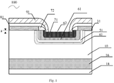
- Fig. 1 is a schematic view of the insulated gate bipolar transistor 100 in an embodiment, which includes a peripheral terminal structure (not shown in Fig. 1 ) and an active region surrounded by the terminal structure.
- a substrate of the insulated gate bipolar transistor 100 is an N-type substrate 10.
- a back side of the substrate 10 is disposed with a P-type region 16, a back side of the P-type region 16 is disposed with a backside metal structure 18, and a terminal guard ring (not shown in Fig. 1 ) is disposed in the terminal structure.
- a front side of the substrate 10 of the active region is disposed with a poly silicon gate 31, both sides of the poly silicon gate 31 on the substrate 10 are disposed with the spacers 72, an interlayer dielectric 81 covering the poly silicon gate 31 and the spacers 72 is disposed on the substrate 10, and the interlayer dielectric 81 is covered by a metal lead layer 91.
- An N-type carrier enhanced region 41 is disposed in the substrate 10 of the active region, a P-body region 51 is disposed in the carrier enhanced region 41, an N-type heavily doped region 61 is disposed in the P-body region 51, a P-type heavily doped region71 is disposed in the N-type heavily doped region 61, a dishing area 62 dishing inwardly is formed at a surface of the P-type heavily doped region 71, and an inwardly dishing depth (i.e. a in Fig. 1 ) of the dishing area 62 with respect to the substrates at both sides is 0.15 micron to 0.3 micron.
- a method of manufacturing the insulated gate bipolar transistor 100 described above is also provided in the invention, which includes the following steps:
- step S110 a substrate is provided, a field oxide layer is formed at a front side of the substrate and a terminal guard ring is formed.
- the substrate 10 is made of silicon, silicon carbide, gallium arsenide, indium phosphide orgermanium-silicon.
- the substrate 10 is made of monocrystal silicon wafer with a crystal orientation of ⁇ 100>.
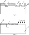
- a field oxide layer 20 is grown at the front side of the substrate 10, then the field oxide layer 20 is photoetched and etched directly above the substrate 10 required to form the terminal guard ring by using a terminal guard ring photomask. Then the terminal guard ring is formed through implanting of the P-type ions by using the field oxide layer 20 as a masking layer.
- Three terminal guard rings 21, 22, 23 are shown in Fig. 3A , wherein a position where the terminal guard ring23 is located is adjacent to the active region area in the center of the substrate 10. It should be understood that the number of the terminal guard rings is not limited to the present embodiment, and can be selected and configured according to actual requirement for the device by those skilled in the art.
- Fig. 3A is a partial cross-section view of the insulated gate bipolar transistor after the step S110 is performed in the embodiment.
- the P-type ions implanted in the step S110 are boron ions. It should be understood that the particularly implanted P-type/N-type ions given in each step of implanting of ions in the embodiment are only better embodiments, and in other embodiments they can be replaced with other P-type/N-type ions well known by those skilled in the art.
- step S120 the field oxide layer of the active region area is photoetched and etched by using the active region photomask, and the N-type ions are implanted to the substrate by using a photoresist as a mask film.
- the field oxide layer 20 of the active region area is photoetched and etched by using the active region photomask, then the photoresist is not removed and the N-type ions are implanted to the substrate 10 by using the photoresist as a mask film.
- the N-type ions implanted in step S120 are phosphorous ions.
- Fig. 3B is apartial cross-section view of the insulated gate bipolar transistor after the step S120 is performed in the embodiment, the structure shown by which is located at the right side of Fig. 3A .
- step S130 a polysilicon gate is deposited and formed on the substrate where the field oxide layer is etched, and a protecting layer is formed on the polysilicon gate.
- Polysilicon is deposited on the substrate 10 where the field oxide layer 20 is etched, the protecting layer is formed on the deposited polysilicon, and the polysilicon gate 31 is formed by photoetching and etching surplus polysilicon and the protecting layer by using a polysilicon photomask.
- the protecting layer is a silicon nitride layer 32, wherein prior to depositing silicon nitride it needs to perform one time oxidation.
- a first oxide layer (not shown in Fig. 3C ) is formed at a surface of the deposited polysilicon, and then the silicon nitride layer 32 is formed on the first oxide layer by depositing the silicon nitride.
- a first oxide layer is deposited between the polysilicon gate 31 and the silicon nitride layer 32, which can improve the issue related to stress.
- Fig. 3C is a partial cross-section view of the insulated gate bipolar transistor after the step S130 is performed in the embodiment.
- step S140 a carrier enhanced region is formed after driving-in an implantation area of N-type ions.
- the carrier enhanced region 41 is formed by the implantation area of N-type ions in step S120 after which is drived-in.
- the order of steps S130 and S140 can be changed, that is to say, after the step S120 of implanting N-type ions, firstly a high temperature driving-in process is performed to form the carrier enhanced region 41, and then the polysilicon gate 31 and the silicon nitride layer 32 are formed.
- step S150 the carrier enhanced region is photoetched by using a P well photomask and P-type ions are implanted to the carrier enhanced region, and then a P-body region is formed after performing a driving-in process.
- the P-type ions implanted in step S150 are boron ions, and the P-body region 51 is formed after performing the high temperature driving-in process.
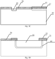
- Fig. 3D is a partial cross-section view of the insulated gate bipolar transistor after the step S150 is performed in the embodiment, the structure shown by which is located at the right side of Fig. 3C .
- step S160 N-type ions are self-alignedly implanted to the P-body region by using the polysilicon gate, and an N-type heavily doped region is formed after performing a driving-in process.
- the N-type ions implanted in step S160 are arsenic ions, and the N-type heavily doped region (NSD) 61 is formed after performing the high temperature driving-in process.
- Fig. 3E is a partial cross-section view of the insulated gate bipolar transistor after the step S160 is performed in the embodiment.
- step S170 a spacer is formed at both sides of the polysilicon gate, then P-type ions are implanted to the N-type heavily doped region, and a P-type heavily doped region is formed after performing a driving-in process.
- a second oxide layer is deposited, then a spacer corrosion process is performed for the device to corrode a surplus of the second oxide layer, for forming the spacer 72 at both sides of the polysilicon gate 31.
- the method further comprises silicon-etching the N-type heavily doped region 61 and forming a dishing area.
- the dishing area 62 is a shallow dishing the inwardly dishing depth of which is 0.15 micron to 0.3 micron.
- the shallow dishing (the dishing area 62) of 0.15 micron to 0.3 micron is formed by etching the P-type heavily doped region, which results in a better impurity distribution and a greater metal contacting area for the device, reducing the power consumption, improving reliability of product, and further reducing the conduction voltage drop.
- the P-type ions are implanted.
- the implanted P-type ions are boron ions.
- the high temperature driving-in process is performed to form the P-type heavily doped region (PSD) 71.
- step S180 the implantation and doping processes are performed for the polysilicon gate after removing the protecting layer.
- the protecting layer in the embodiment is the silicon nitride layer 32.
- the N-type ions are implanted and doped to the polysilicon gate 31.
- the implantation and doping processes for the polysilicon gate are performed after performing the photoetching process by using the polysilicon photomask.
- Fig. 3F is a partial cross-section view of the insulated gate bipolar transistor after the step S180 is performed in the embodiment.
- the interlayer dielectric can be generated regularly, and the processes of frontside metallization, backgrinding, implantation and annealing, backside metallization and so on can be performed.
- ILD interlayer dielectric
- step S190 an interlayer dielectric covering the surfaces of the polysilicon gate and the spacer is formed.
- BPSG borophosphosilicate glass
- step S200 the frontside metallization process is performed.
- a contact hole is formed by performing photoetching and etching processes by using a contact hole photomask, and a conductive metal is sputtered at the surface of the device, then the conductive metal is etched by using a metal photomask, and a metal lead layer 91 covering the interlayer dielectric 81 is formed.
- step S210 the processes of backgrinding, P-type ions implantation and annealing are performed.
- the back side of the substrate 10 is ground to the required thickness, the P-type ions are implanted to the back side of the substrate 10 and the annealing process is performed, for forming a P-body region 16.
- a substrate PN junction is formed by the P-body region 16 and the substrate 10.
- the P-type ions implanted in the step S210 are boron ions.
- step S220 the backside metallization process is performed.
- Fig. 1 is a partial cross-section view of the insulated gate bipolar transistor 100 after the step S220 is performed in the embodiment
- the phosphorous ions is implanted, for increasing the concentration of the carrier in the channel, forming a carrier enhanced region 41 and then reducing the conduction voltage drop.
- the ions implantation of the carrier enhanced region 41 directly uses the photoresist formed by photoetching in the step S120 as the mask film, and it does not need to manufacture an additional photomask for the ions implantation of the carrier enhanced region 41, which saving cost.
- implanting and doping for the polysilicon gate 31 is performed, thus such implanting and doping processes are performed after the above five high temperature driving-in processes are performed, avoiding the influence of the doped ions in the polysilicon during such high temperature processes to the gate oxide and channel region, and solving the difficult problem that the gate oxide can be destroyed easily during the hot process.
- the method of manufacturing the insulated gate bipolar transistor is compatible with the DMOS process, and has the advantages of universality, portability for different IC production lines and so on.
- the PSD implantation can be also performed again, for implanting P-type ions to the P-type heavily doped region to obtain a good ohm contact and improve performance of the device.
Landscapes
- Electrodes Of Semiconductors (AREA)
- Metal-Oxide And Bipolar Metal-Oxide Semiconductor Integrated Circuits (AREA)
- Engineering & Computer Science (AREA)
- Manufacturing & Machinery (AREA)
Abstract
Description
- The present invention relates to a method of manufacturing a semiconductor device, and particularly relates to a method of manufacturing an insulated gate bipolar transistor.
- The insulated gate bipolar transistor (IGBT) generally is a power semiconductor device consisting of a bipolar junction transistor (BJT) and a metal oxide semiconductor field effect transistor (MOS).A conduction voltage drop of a conventional insulated gate bipolar transistor is relatively high.
- On the basis of this, it is necessary to provide a method of manufacturing an insulated gate bipolar transistor to manufacture an insulated gate bipolar transistor with a low conduction voltage drop.
- A method of manufacturing an insulated gate bipolar transistor comprises: providing a substrate, forming a field oxide layer at a front side of the substrate, photoetching and etching the field oxide layer by using a terminal guard ring photomask, and forming a terminal guard ring by implanting P-type ions to the substrate under the etched area; photoetching and etching the field oxide layer of an active region by using an active region photomask, implanting N-type ions to the substrate by using a photoresist as a mask film, and depositing polysilicon on the substrate where the field oxide layer being etched, forming a protecting layer on the deposited polysilicon; forming a polysilicon gate by photoetching and etching surplus polysilicon and the protecting layer by using a polysilicon photomask, forming a carrier enhanced region after driving-in an implantation area of N-type ions; or photoetching and etching the field oxide layer of the active region by using the active region photomask, implanting N-type ions to the substrate by using the photoresist as the mask film, and then forming the carrier enhanced region after performing a driving-in process, and depositing polysilicon on the substrate where the field oxide layer being etched, forming the protecting layer on the deposited polysilicon, forming a polysilicon gate by photoetching and etching surplus polysilicon and the protecting layer by using a polysilicon photomask; photoetching the carrier enhanced region by using a P well photomask and implanting P-type ions to the carrier enhanced region, and forming a P-body region after performing a driving-in process; self-alignedly implanting N-type ions to the P-body region by using the polysilicon gate, and forming an N-type heavily doped region after performing a driving-in process; forming a spacer at both sides of the polysilicon gate, then implanting P-type ions to the N-type heavily doped region, and forming a P-type heavily doped region after performing a driving-in process; implanting and doping polysilicon to the polysilicon gate after removing the protecting layer; and forming an interlayer dielectric, performing a frontside metalized process of the insulated gate bipolar transistor, performing backgrinding, implanting of P-type ions and an annealing process, and performing a backside metalized process of the insulated gate bipolar transistor.
- In one of embodiments, after forming the spacer at both sides of the polysilicon gate and prior to implanting-type ions to the N-type heavily doped region, the method further comprises forming a dishing area by etching the N-type heavily doped region, wherein an inwardly dishing depth of the dishing area with respect to the substrates of both sides is 0.15 micron to 0.3 micron.
- In one of embodiments, forming the protecting layer on the deposited polysilicon comprises forming a first oxide layer at a surface of the polysilicon, and depositing a silicon nitride layer at a surface of the first oxide layer.
- In one of embodiments, after performing the frontside metalized process of the insulated gate bipolar transistor, the method further comprises implanting P-type ions to the P-type heavily doped region again.
- In one of embodiments, in the step of forming the terminal guard ring by implanting P-type ions to the substrate under the etched area, the P-type ions are boron ions; in the step of implanting N-type ions to the substrate by using a photoresist as a mask film, the N-type ions are phosphorous ions; in the step of photoetching the carrier enhanced region by using a P well photomask and implanting P-type ions to the carrier enhanced region, the P-type ions are boron ions; in the step of self-alignedly implanting N-type ions to the P-body region by using the polysilicon gate, the N-type ions are arsenic ions; in the step of implanting P-type ions to the N-type heavily doped region, the P-type ions are boron ions; in the step of implanting and doping polysilicon to the polysilicon gate after removing the protecting layer, the implanted ions are phosphorous ions.
- In one of embodiments, forming the spacer at both sides of the polysilicon gate comprises: depositing a second oxide layer, then removing a surplus of the second oxide layer by corroding, and forming the spacer by using the remaining part of the second oxide layer.
- In one of embodiments, performing the frontside metalized process of the insulated gate bipolar transistor comprises forming a contact hole by performing photoetching and etching processes by using a contact hole photomask, and sputtering a conductive metal on the interlayer dielectric, then forming a metal lead layer covering the interlayer dielectric by photoetching and etching the sputtered metal by using a metal photomask.
- In one of embodiments, the substrate is made of silicon, silicon carbide, gallium arsenide, indium phosphide orgermanium-silicon.
- In one of embodiments, the substrate is made of monocrystal silicon with a crystal orientation of <100>.
- In one of embodiments, forming the interlayer dielectric comprises depositing borophosphosilicate glass and performing a hot reflow process, then forming the interlayer dielectric covering the surfaces of the polysilicon gate and the spacer.
- In the method of manufacturing the insulated gate bipolar transistor described above, when a field oxide layer of an active region area is etched by using an active region photomask, implantation of N-type ions is performed, for increasing a concentration of carriers in a channel to form a carrier enhanced region and then reduce the conduction voltage drop.
-
-
Fig. 1 is a schematic view of the insulated gate bipolar transistor in an embodiment; -
Fig. 2 shows a flow chart of a method of manufacturing the insulated gate bipolar transistor in an embodiment; -
Figs. 3A to 3F are partial cross-section views during manufacturing the insulated gate bipolar transistor by using the method of manufacturing the insulated gate bipolar transistor in an embodiment. - The details of one or more embodiments of the invention are set forth in the accompanying drawings and the description below. Other features, objects, and advantages of the invention will be apparent from the description and drawings, and from the claims.
-
Fig. 1 is a schematic view of the insulated gatebipolar transistor 100 in an embodiment, which includes a peripheral terminal structure (not shown inFig. 1 ) and an active region surrounded by the terminal structure. A substrate of the insulated gatebipolar transistor 100 is an N-type substrate 10. A back side of thesubstrate 10 is disposed with a P-type region 16, a back side of the P-type region 16 is disposed with abackside metal structure 18, and a terminal guard ring (not shown inFig. 1 ) is disposed in the terminal structure. A front side of thesubstrate 10 of the active region is disposed with apoly silicon gate 31, both sides of thepoly silicon gate 31 on thesubstrate 10 are disposed with thespacers 72, an interlayer dielectric 81 covering thepoly silicon gate 31 and thespacers 72 is disposed on thesubstrate 10, and the interlayer dielectric 81 is covered by ametal lead layer 91. An N-type carrier enhancedregion 41 is disposed in thesubstrate 10 of the active region, a P-body region 51 is disposed in the carrier enhancedregion 41, an N-type heavily dopedregion 61 is disposed in the P-body region 51, a P-type heavily doped region71 is disposed in the N-type heavily dopedregion 61, adishing area 62 dishing inwardly is formed at a surface of the P-type heavily dopedregion 71, and an inwardly dishing depth (i.e. a inFig. 1 ) of thedishing area 62 with respect to the substrates at both sides is 0.15 micron to 0.3 micron. - Referring to
Fig. 2 , a method of manufacturing the insulated gatebipolar transistor 100 described above is also provided in the invention, which includes the following steps: - In step S110, a substrate is provided, a field oxide layer is formed at a front side of the substrate and a terminal guard ring is formed.
- The
substrate 10 is made of silicon, silicon carbide, gallium arsenide, indium phosphide orgermanium-silicon. In the embodiment, thesubstrate 10 is made of monocrystal silicon wafer with a crystal orientation of <100>. - In the embodiment, firstly a
field oxide layer 20 is grown at the front side of thesubstrate 10, then thefield oxide layer 20 is photoetched and etched directly above thesubstrate 10 required to form the terminal guard ring by using a terminal guard ring photomask. Then the terminal guard ring is formed through implanting of the P-type ions by using thefield oxide layer 20 as a masking layer. Threeterminal guard rings Fig. 3A , wherein a position where the terminal guard ring23 is located is adjacent to the active region area in the center of thesubstrate 10. It should be understood that the number of the terminal guard rings is not limited to the present embodiment, and can be selected and configured according to actual requirement for the device by those skilled in the art. -
Fig. 3A is a partial cross-section view of the insulated gate bipolar transistor after the step S110 is performed in the embodiment. In the embodiment, the P-type ions implanted in the step S110 are boron ions. It should be understood that the particularly implanted P-type/N-type ions given in each step of implanting of ions in the embodiment are only better embodiments, and in other embodiments they can be replaced with other P-type/N-type ions well known by those skilled in the art. - In step S120, the field oxide layer of the active region area is photoetched and etched by using the active region photomask, and the N-type ions are implanted to the substrate by using a photoresist as a mask film.
- The
field oxide layer 20 of the active region area is photoetched and etched by using the active region photomask, then the photoresist is not removed and the N-type ions are implanted to thesubstrate 10 by using the photoresist as a mask film. In the embodiment, the N-type ions implanted in step S120 are phosphorous ions.Fig. 3B is apartial cross-section view of the insulated gate bipolar transistor after the step S120 is performed in the embodiment, the structure shown by which is located at the right side ofFig. 3A . - In step S130, a polysilicon gate is deposited and formed on the substrate where the field oxide layer is etched, and a protecting layer is formed on the polysilicon gate.
- Polysilicon is deposited on the
substrate 10 where thefield oxide layer 20 is etched, the protecting layer is formed on the deposited polysilicon, and thepolysilicon gate 31 is formed by photoetching and etching surplus polysilicon and the protecting layer by using a polysilicon photomask. In the embodiment, the protecting layer is asilicon nitride layer 32, wherein prior to depositing silicon nitride it needs to perform one time oxidation. A first oxide layer (not shown inFig. 3C ) is formed at a surface of the deposited polysilicon, and then thesilicon nitride layer 32 is formed on the first oxide layer by depositing the silicon nitride. Compared to depositing the silicon nitride directly on the surface of the polysilicon, a first oxide layer is deposited between thepolysilicon gate 31 and thesilicon nitride layer 32, which can improve the issue related to stress. -
Fig. 3C is a partial cross-section view of the insulated gate bipolar transistor after the step S130 is performed in the embodiment. - In step S140, a carrier enhanced region is formed after driving-in an implantation area of N-type ions.
- The carrier enhanced
region 41 is formed by the implantation area of N-type ions in step S120 after which is drived-in. - In other embodiments, the order of steps S130 and S140 can be changed, that is to say, after the step S120 of implanting N-type ions, firstly a high temperature driving-in process is performed to form the carrier enhanced
region 41, and then thepolysilicon gate 31 and thesilicon nitride layer 32 are formed. - In step S150, the carrier enhanced region is photoetched by using a P well photomask and P-type ions are implanted to the carrier enhanced region, and then a P-body region is formed after performing a driving-in process.
- In the embodiment, the P-type ions implanted in step S150 are boron ions, and the P-
body region 51 is formed after performing the high temperature driving-in process.Fig. 3D is a partial cross-section view of the insulated gate bipolar transistor after the step S150 is performed in the embodiment, the structure shown by which is located at the right side ofFig. 3C . - In step S160, N-type ions are self-alignedly implanted to the P-body region by using the polysilicon gate, and an N-type heavily doped region is formed after performing a driving-in process.
- In the embodiment, the N-type ions implanted in step S160 are arsenic ions, and the N-type heavily doped region (NSD) 61 is formed after performing the high temperature driving-in process.
Fig. 3E is a partial cross-section view of the insulated gate bipolar transistor after the step S160 is performed in the embodiment. - In step S170, a spacer is formed at both sides of the polysilicon gate, then P-type ions are implanted to the N-type heavily doped region, and a P-type heavily doped region is formed after performing a driving-in process.
- Firstly a second oxide layer is deposited, then a spacer corrosion process is performed for the device to corrode a surplus of the second oxide layer, for forming the
spacer 72 at both sides of thepolysilicon gate 31. - In the embodiment, after forming the
spacer 72, and prior to implanting the P-type ions to the N-type heavily dopedregion 61, the method further comprises silicon-etching the N-type heavily dopedregion 61 and forming a dishing area. The dishingarea 62 is a shallow dishing the inwardly dishing depth of which is 0.15 micron to 0.3 micron. - Prior to implanting the P-type ions to the N-type heavily doped
region 61, the shallow dishing (the dishing area 62) of 0.15 micron to 0.3 micron is formed by etching the P-type heavily doped region, which results in a better impurity distribution and a greater metal contacting area for the device, reducing the power consumption, improving reliability of product, and further reducing the conduction voltage drop. - After forming the etched dishing
area 62, the P-type ions are implanted. In the embodiment, the implanted P-type ions are boron ions. After performing the implantation process, the high temperature driving-in process is performed to form the P-type heavily doped region (PSD) 71. - In step S180, the implantation and doping processes are performed for the polysilicon gate after removing the protecting layer.
- As mentioned previously, the protecting layer in the embodiment is the
silicon nitride layer 32. After removing thesilicon nitride layer 32 at the surface of thepolysilicon gate 31, the N-type ions are implanted and doped to thepolysilicon gate 31. In the embodiment, the implantation and doping processes for the polysilicon gate are performed after performing the photoetching process by using the polysilicon photomask.Fig. 3F is a partial cross-section view of the insulated gate bipolar transistor after the step S180 is performed in the embodiment. - After the step S180 is performed, the interlayer dielectric (ILD) can be generated regularly, and the processes of frontside metallization, backgrinding, implantation and annealing, backside metallization and so on can be performed. Similarly, a specific embodiment is described as follows:
- In step S190, an interlayer dielectric covering the surfaces of the polysilicon gate and the spacer is formed.
- After depositing borophosphosilicate glass (BPSG) at the surface of the device, a hot reflow process is performed, for forming the
interlayer dielectric 81 covering the surfaces of thepolysilicon gate 31 and thespacer 72. - In step S200, the frontside metallization process is performed.
- A contact hole is formed by performing photoetching and etching processes by using a contact hole photomask, and a conductive metal is sputtered at the surface of the device, then the conductive metal is etched by using a metal photomask, and a
metal lead layer 91 covering theinterlayer dielectric 81 is formed. - In step S210, the processes of backgrinding, P-type ions implantation and annealing are performed.
- The back side of the
substrate 10 is ground to the required thickness, the P-type ions are implanted to the back side of thesubstrate 10 and the annealing process is performed, for forming a P-body region 16. A substrate PN junction is formed by the P-body region 16 and thesubstrate 10. In the embodiment, the P-type ions implanted in the step S210 are boron ions. - In step S220, the backside metallization process is performed.
- The conductive metal is sputtered at the back side of the
substrate 10, and abackside metal structure 18 is formed at the surface of the P-type region 16 as the collector metal lead.Fig. 1 is a partial cross-section view of the insulated gatebipolar transistor 100 after the step S220 is performed in the embodiment - In the method of manufacturing an insulated gate bipolar transistor described above, when the
field oxide layer 20 of the active region area is etched by using the active region photomask in the step S120, the phosphorous ions is implanted, for increasing the concentration of the carrier in the channel, forming a carrier enhancedregion 41 and then reducing the conduction voltage drop. - Six photomasks are used during the above manufacturing process, and are the terminal guard ring photomask, the active region photomask, the polysilicon photomask, the P well photomask, the contact hole photomask and the metal photomask. The ions implantation of the carrier enhanced
region 41 directly uses the photoresist formed by photoetching in the step S120 as the mask film, and it does not need to manufacture an additional photomask for the ions implantation of the carrier enhancedregion 41, which saving cost. - Further, after the P-type heavily doped
region 71 is manufactured, implanting and doping for thepolysilicon gate 31 is performed, thus such implanting and doping processes are performed after the above five high temperature driving-in processes are performed, avoiding the influence of the doped ions in the polysilicon during such high temperature processes to the gate oxide and channel region, and solving the difficult problem that the gate oxide can be destroyed easily during the hot process. Meanwhile, the method of manufacturing the insulated gate bipolar transistor is compatible with the DMOS process, and has the advantages of universality, portability for different IC production lines and so on. - In one of embodiments, after forming the contact hole by performing photoetching and etching processes by using the contact hole photomask in step S200, and prior to sputtering a metal, the PSD implantation can be also performed again, for implanting P-type ions to the P-type heavily doped region to obtain a good ohm contact and improve performance of the device.
- Although the invention is illustrated and described herein with reference to specific embodiments, the invention is not intended to be limited to the details shown. Rather, various modifications may be made in the details within the scope and range of equivalents of the claims and without departing from the invention.
Claims (10)
- A method of manufacturing an insulated gate bipolar transistor, comprising:providing a substrate, forming a field oxide layer at a front side of the substrate, photoetching and etching the field oxide layer by using a terminal guard ring photomask, and forming a terminal guard ring by implanting P-type ions into the substrate under an etched area;photoetching and etching the field oxide layer on an active region by using an active region photomask, implanting N-type ions to the substrate by using a photoresist as a mask film, and depositing polysilicon on the substrate where the field oxide layer being etched, forming a protecting layer on the deposited polysilicon; forming a polysilicon gate by photoetching and etching surplus polysilicon and the protecting layer by using a polysilicon photomask, forming a carrier enhanced region after driving-in an implantation area of N-type ions; or photoetching and etching the field oxide layer of the active region by using the active region photomask, implanting N-type ions to the substrate by using the photoresist as the mask film, and then forming the carrier enhanced region after performing a driving-in process, and depositing polysilicon on the substrate where the field oxide layer being etched, forming the protecting layer on the deposited polysilicon, forming a polysilicon gate by photoetching and etching surplus polysilicon and the protecting layer by using a polysilicon photomask;photoetching the carrier enhanced region by using a P well photomask and implanting P-type ions to the carrier enhanced region, and forming a P-type body region after performing a driving-in process;self-alignedly implanting N-type ions to the P-body region by using the polysilicon gate, and forming an N-type heavily doped region after performing a driving-in process;forming a spacer at both sides of the polysilicon gate, then implanting P-type ions to the N-type heavily doped region, and forming a P-type heavily doped region after performing a driving-in process;implanting and doping polysilicon to the polysilicon gate after removing the protecting layer; andforming an interlayer dielectric, performing a frontside metalized process of the insulated gate bipolar transistor, performing backgrinding, implanting of P-type ions and an annealing process, and performing a backside metalized process of the insulated gate bipolar transistor.
- The method of manufacturing the insulated gate bipolar transistor of claim 1, characterized in that, after forming the spacer at both sides of the polysilicon gate and prior to implanting P-type ions to the N-type heavily doped region, the method further comprises forming a dishing area by etching the N-type heavily doped region, wherein an inwardly dishing depth of the dishing area with respect to the substrates at both sides is 0.15 micron to 0.3 micron.
- The method of manufacturing the insulated gate bipolar transistor of claim 1, characterized in that, forming the protecting layer on the deposited polysilicon comprises forming a first oxide layer at a surface of the polysilicon, and depositing a silicon nitride layer at a surface of the first oxide layer.
- The method of manufacturing the insulated gate bipolar transistor of claim 1, characterized in that, after performing the frontside metalized process of the insulated gate bipolar transistor, the method further comprises implanting P-type ions to the P-type heavily doped region again.
- The method of manufacturing the insulated gate bipolar transistor of claim 1, characterized in that, in the step of forming the terminal guard ring by implanting P-type ions to the substrate under the etched area, the P-type ions are boron ions; in the step of implanting N-type ions to the substrate by using a photoresist as a mask film, the N-type ions are phosphorous ions; in the step of photoetching the carrier enhanced region by using a P well photomask and implanting P-type ions to the carrier enhanced region, the P-type ions are boron ions; in the step of self-alignedly implanting N-type ions to the P-body region by using the polysilicon gate, the N-type ions are arsenic ions; in the step of implanting P-type ions to the N-type heavily doped region, the P-type ions are boron ions; in the step of implanting and doping polysilicon to the polysilicon gate after removing the protecting layer, the implanted ions are phosphorous ions.
- The method of manufacturing the insulated gate bipolar transistor of claim 1, characterized in that, forming the spacer at both sides of the polysilicon gate comprises: depositing a second oxide layer, then removing a surplus of the second oxide layer by corroding, and forming the spacer by using the remaining part of the second oxide layer.
- The method of manufacturing the insulated gate bipolar transistor of claim 1, characterized in that, performing the frontside metalized process of the insulated gate bipolar transistor comprises forming a contact hole by performing photoetching and etching processes by using a contact hole photomask, and sputtering a conductive metal on the interlayer dielectric, then forming a metal lead layer covering the interlayer dielectric by photoetching and etching the sputtered metal by using a metal photomask.
- The method of manufacturing the insulated gate bipolar transistor of claim 1, characterized in that, the substrate is made of silicon, silicon carbide, gallium arsenide, indium phosphide orgermanium-silicon.
- The method of manufacturing the insulated gate bipolar transistor of claim 8, characterized in that, the substrate is made of monocrystal silicon with a crystal orientation of <100>.
- The method of manufacturing the insulated gate bipolar transistor of claim 8, characterized in that, forming the interlayer dielectric comprises depositing borophosphosilicate glass and performing a hot reflow process, then forming the interlayer dielectric covering the surfaces of the polysilicon gate and the spacer.
Applications Claiming Priority (2)
| Application Number | Priority Date | Filing Date | Title |
|---|---|---|---|
| CN201310380034.3A CN104425247B (en) | 2013-08-27 | 2013-08-27 | A kind of preparation method of insulated gate bipolar transistor |
| PCT/CN2014/085094 WO2015027881A1 (en) | 2013-08-27 | 2014-08-25 | Method for manufacturing insulated gate bipolar transistor |
Publications (3)
| Publication Number | Publication Date |
|---|---|
| EP3041036A1 true EP3041036A1 (en) | 2016-07-06 |
| EP3041036A4 EP3041036A4 (en) | 2017-01-25 |
| EP3041036B1 EP3041036B1 (en) | 2020-04-22 |
Family
ID=52585578
Family Applications (1)
| Application Number | Title | Priority Date | Filing Date |
|---|---|---|---|
| EP14839057.8A Active EP3041036B1 (en) | 2013-08-27 | 2014-08-25 | Method for manufacturing insulated gate bipolar transistor |
Country Status (4)
| Country | Link |
|---|---|
| US (1) | US9590029B2 (en) |
| EP (1) | EP3041036B1 (en) |
| CN (1) | CN104425247B (en) |
| WO (1) | WO2015027881A1 (en) |
Families Citing this family (3)
| Publication number | Priority date | Publication date | Assignee | Title |
|---|---|---|---|---|
| CN112309863B (en) * | 2019-07-31 | 2024-02-23 | 上海积塔半导体有限公司 | Ultralow on-resistance LDMOS and manufacturing method thereof |
| GB2588663A (en) * | 2019-10-31 | 2021-05-05 | Mqsemi Ag | Semiconductor device and method of manufacturing thereof |
| CN115241063A (en) * | 2022-07-04 | 2022-10-25 | 江苏东海半导体股份有限公司 | Preparation method of insulated gate bipolar transistor |
Family Cites Families (19)
| Publication number | Priority date | Publication date | Assignee | Title |
|---|---|---|---|---|
| US4567641A (en) | 1982-04-12 | 1986-02-04 | General Electric Company | Method of fabricating semiconductor devices having a diffused region of reduced length |
| US5468982A (en) | 1994-06-03 | 1995-11-21 | Siliconix Incorporated | Trenched DMOS transistor with channel block at cell trench corners |
| GB2303487A (en) * | 1995-07-21 | 1997-02-19 | Plessey Semiconductors Ltd | Semiconductor devices with recessed emitters |
| US5843796A (en) * | 1995-09-11 | 1998-12-01 | Delco Electronics Corporation | Method of making an insulated gate bipolar transistor with high-energy P+ im |
| US6429481B1 (en) | 1997-11-14 | 2002-08-06 | Fairchild Semiconductor Corporation | Field effect transistor and method of its manufacture |
| US6403432B1 (en) * | 2000-08-15 | 2002-06-11 | Taiwan Semiconductor Manufacturing Company | Hardmask for a salicide gate process with trench isolation |
| US20030010998A1 (en) | 2001-07-10 | 2003-01-16 | Motorola, Inc. | Apparatus and techniques for implementing wireless communication between integrated transmitters and integrated receivers |
| US6714768B2 (en) * | 2001-08-06 | 2004-03-30 | Motorola, Inc. | Structure and method for fabricating semiconductor structures and polarization modulator devices utilizing the formation of a compliant substrate |
| US6831329B2 (en) * | 2001-10-26 | 2004-12-14 | Fairchild Semiconductor Corporation | Quick punch through IGBT having gate-controllable DI/DT and reduced EMI during inductive turn off |
| US6979861B2 (en) * | 2002-05-30 | 2005-12-27 | Apd Semiconductor, Inc. | Power device having reduced reverse bias leakage current |
| JP4166102B2 (en) * | 2003-02-26 | 2008-10-15 | トヨタ自動車株式会社 | High voltage field effect semiconductor device |
| JP2006041023A (en) | 2004-07-23 | 2006-02-09 | Toshiba Corp | Semiconductor device and manufacturing method thereof |
| US20080157117A1 (en) * | 2006-12-28 | 2008-07-03 | Mcnutt Ty R | Insulated gate bipolar transistor with enhanced conductivity modulation |
| CN101226961A (en) | 2008-01-29 | 2008-07-23 | 电子科技大学 | Thin film SOI thick gate oxide power device with source field plate |
| CN100568534C (en) | 2008-01-29 | 2009-12-09 | 电子科技大学 | Thin film SOI thick gate oxide power device with gate field plate |
| CN102496573B (en) * | 2011-12-28 | 2014-01-01 | 上海先进半导体制造股份有限公司 | Trench insulated gate bipolar transistor and its fabrication method |
| CN102522335B (en) | 2011-12-31 | 2014-10-22 | 杭州士兰集成电路有限公司 | Power device terminal ring production method and structure of terminal ring |
| CN102956687A (en) | 2012-10-30 | 2013-03-06 | 浙江大学 | SOI-LIGBT (Silicon on Insulator-Lateral Insulated-Gate Bipolar Transistor) device based on double channel structure |
| CN102969243B (en) * | 2012-12-07 | 2015-04-22 | 株洲南车时代电气股份有限公司 | Plane gate type IGBT (Insulated Gate Bipolar Translator) chip production method |
-
2013
- 2013-08-27 CN CN201310380034.3A patent/CN104425247B/en active Active
-
2014
- 2014-08-25 WO PCT/CN2014/085094 patent/WO2015027881A1/en not_active Ceased
- 2014-08-25 US US14/902,432 patent/US9590029B2/en active Active
- 2014-08-25 EP EP14839057.8A patent/EP3041036B1/en active Active
Non-Patent Citations (1)
| Title |
|---|
| See references of WO2015027881A1 * |
Also Published As
| Publication number | Publication date |
|---|---|
| US20160380048A1 (en) | 2016-12-29 |
| CN104425247B (en) | 2018-01-23 |
| WO2015027881A1 (en) | 2015-03-05 |
| EP3041036B1 (en) | 2020-04-22 |
| CN104425247A (en) | 2015-03-18 |
| US9590029B2 (en) | 2017-03-07 |
| EP3041036A4 (en) | 2017-01-25 |
Similar Documents
| Publication | Publication Date | Title |
|---|---|---|
| US11824090B2 (en) | Back side dopant activation in field stop IGBT | |
| US8536003B2 (en) | Method for fabricating semiconductor power device | |
| US9502497B2 (en) | Method for preparing power diode | |
| US9620584B2 (en) | Integrated Schottky diode in high voltage semiconductor device | |
| CN103107194A (en) | Trench power transistor assembly and manufacturing method thereof | |
| US7649222B2 (en) | Semiconductor device | |
| CN104576361B (en) | The preparation method of power diode | |
| US8492221B2 (en) | Method for fabricating power semiconductor device with super junction structure | |
| KR20180104236A (en) | Method of Manufacturing Power Semiconductor Device | |
| CN102779756A (en) | Method for manufacturing semiconductor power device | |
| US9590029B2 (en) | Method for manufacturing insulated gate bipolar transistor | |
| US10084036B2 (en) | Insulated gate bipolar transistor and manufacturing method therefor | |
| US9502534B2 (en) | Preparation method for power diode | |
| CN108389857B (en) | Polysilicon dummy gate electrostatic discharge device for improving holding voltage and manufacturing method thereof | |
| CN117650179B (en) | Shielded gate field effect transistor and preparation method thereof | |
| CN116565004B (en) | Radio frequency semiconductor device and manufacturing method thereof | |
| CN102931081B (en) | Manufacturing method for semiconductor device with field barrier layer | |
| CN210443554U (en) | Shielded gate trench MOSFET with integrated ESD protection | |
| KR101928253B1 (en) | Method of Manufacturing Power Semiconductor Device | |
| CN108281486B (en) | A kind of avalanche endurance enhanced VDMOS device structure and fabrication method thereof | |
| CN108110044A (en) | Semiconductor power device and preparation method thereof | |
| US10608099B2 (en) | Methods of manufacturing semiconductor devices with a deep barrier layer | |
| KR20150144035A (en) | Apparatus and method for manufacturing a power semiconductor device | |
| CN121712043A (en) | A MOS device and its fabrication method | |
| CN119170625A (en) | A semiconductor device with self-aligned channel and self-aligned contact area and its preparation |
Legal Events
| Date | Code | Title | Description |
|---|---|---|---|
| PUAI | Public reference made under article 153(3) epc to a published international application that has entered the european phase |
Free format text: ORIGINAL CODE: 0009012 |
|
| 17P | Request for examination filed |
Effective date: 20151230 |
|
| AK | Designated contracting states |
Kind code of ref document: A1 Designated state(s): AL AT BE BG CH CY CZ DE DK EE ES FI FR GB GR HR HU IE IS IT LI LT LU LV MC MK MT NL NO PL PT RO RS SE SI SK SM TR |
|
| AX | Request for extension of the european patent |
Extension state: BA ME |
|
| DAX | Request for extension of the european patent (deleted) | ||
| A4 | Supplementary search report drawn up and despatched |
Effective date: 20170103 |
|
| RIC1 | Information provided on ipc code assigned before grant |
Ipc: H01L 21/331 20060101AFI20161221BHEP Ipc: H01L 29/739 20060101ALI20161221BHEP Ipc: H01L 29/06 20060101ALI20161221BHEP Ipc: H01L 29/10 20060101ALI20161221BHEP |
|
| STAA | Information on the status of an ep patent application or granted ep patent |
Free format text: STATUS: EXAMINATION IS IN PROGRESS |
|
| 17Q | First examination report despatched |
Effective date: 20190528 |
|
| GRAP | Despatch of communication of intention to grant a patent |
Free format text: ORIGINAL CODE: EPIDOSNIGR1 |
|
| STAA | Information on the status of an ep patent application or granted ep patent |
Free format text: STATUS: GRANT OF PATENT IS INTENDED |
|
| INTG | Intention to grant announced |
Effective date: 20191128 |
|
| RIN1 | Information on inventor provided before grant (corrected) |
Inventor name: WANG, GENYI Inventor name: DENG, XIAOSHE Inventor name: ZHOU, DONGFEI Inventor name: ZHONG, SHENGRONG |
|
| RAP1 | Party data changed (applicant data changed or rights of an application transferred) |
Owner name: CSMC TECHNOLOGIES FAB2 CO., LTD. |
|
| GRAS | Grant fee paid |
Free format text: ORIGINAL CODE: EPIDOSNIGR3 |
|
| GRAA | (expected) grant |
Free format text: ORIGINAL CODE: 0009210 |
|
| STAA | Information on the status of an ep patent application or granted ep patent |
Free format text: STATUS: THE PATENT HAS BEEN GRANTED |
|
| AK | Designated contracting states |
Kind code of ref document: B1 Designated state(s): AL AT BE BG CH CY CZ DE DK EE ES FI FR GB GR HR HU IE IS IT LI LT LU LV MC MK MT NL NO PL PT RO RS SE SI SK SM TR |
|
| REG | Reference to a national code |
Ref country code: CH Ref legal event code: EP |
|
| REG | Reference to a national code |
Ref country code: DE Ref legal event code: R096 Ref document number: 602014064257 Country of ref document: DE |
|
| REG | Reference to a national code |
Ref country code: IE Ref legal event code: FG4D |
|
| REG | Reference to a national code |
Ref country code: AT Ref legal event code: REF Ref document number: 1261245 Country of ref document: AT Kind code of ref document: T Effective date: 20200515 |
|
| REG | Reference to a national code |
Ref country code: NL Ref legal event code: FP |
|
| REG | Reference to a national code |
Ref country code: LT Ref legal event code: MG4D |
|
| PG25 | Lapsed in a contracting state [announced via postgrant information from national office to epo] |
Ref country code: GR Free format text: LAPSE BECAUSE OF FAILURE TO SUBMIT A TRANSLATION OF THE DESCRIPTION OR TO PAY THE FEE WITHIN THE PRESCRIBED TIME-LIMIT Effective date: 20200723 Ref country code: IS Free format text: LAPSE BECAUSE OF FAILURE TO SUBMIT A TRANSLATION OF THE DESCRIPTION OR TO PAY THE FEE WITHIN THE PRESCRIBED TIME-LIMIT Effective date: 20200822 Ref country code: SE Free format text: LAPSE BECAUSE OF FAILURE TO SUBMIT A TRANSLATION OF THE DESCRIPTION OR TO PAY THE FEE WITHIN THE PRESCRIBED TIME-LIMIT Effective date: 20200422 Ref country code: NO Free format text: LAPSE BECAUSE OF FAILURE TO SUBMIT A TRANSLATION OF THE DESCRIPTION OR TO PAY THE FEE WITHIN THE PRESCRIBED TIME-LIMIT Effective date: 20200722 Ref country code: FI Free format text: LAPSE BECAUSE OF FAILURE TO SUBMIT A TRANSLATION OF THE DESCRIPTION OR TO PAY THE FEE WITHIN THE PRESCRIBED TIME-LIMIT Effective date: 20200422 Ref country code: LT Free format text: LAPSE BECAUSE OF FAILURE TO SUBMIT A TRANSLATION OF THE DESCRIPTION OR TO PAY THE FEE WITHIN THE PRESCRIBED TIME-LIMIT Effective date: 20200422 Ref country code: PT Free format text: LAPSE BECAUSE OF FAILURE TO SUBMIT A TRANSLATION OF THE DESCRIPTION OR TO PAY THE FEE WITHIN THE PRESCRIBED TIME-LIMIT Effective date: 20200824 |
|
| REG | Reference to a national code |
Ref country code: AT Ref legal event code: MK05 Ref document number: 1261245 Country of ref document: AT Kind code of ref document: T Effective date: 20200422 |
|
| PG25 | Lapsed in a contracting state [announced via postgrant information from national office to epo] |
Ref country code: LV Free format text: LAPSE BECAUSE OF FAILURE TO SUBMIT A TRANSLATION OF THE DESCRIPTION OR TO PAY THE FEE WITHIN THE PRESCRIBED TIME-LIMIT Effective date: 20200422 Ref country code: HR Free format text: LAPSE BECAUSE OF FAILURE TO SUBMIT A TRANSLATION OF THE DESCRIPTION OR TO PAY THE FEE WITHIN THE PRESCRIBED TIME-LIMIT Effective date: 20200422 Ref country code: RS Free format text: LAPSE BECAUSE OF FAILURE TO SUBMIT A TRANSLATION OF THE DESCRIPTION OR TO PAY THE FEE WITHIN THE PRESCRIBED TIME-LIMIT Effective date: 20200422 Ref country code: BG Free format text: LAPSE BECAUSE OF FAILURE TO SUBMIT A TRANSLATION OF THE DESCRIPTION OR TO PAY THE FEE WITHIN THE PRESCRIBED TIME-LIMIT Effective date: 20200722 |
|
| PG25 | Lapsed in a contracting state [announced via postgrant information from national office to epo] |
Ref country code: AL Free format text: LAPSE BECAUSE OF FAILURE TO SUBMIT A TRANSLATION OF THE DESCRIPTION OR TO PAY THE FEE WITHIN THE PRESCRIBED TIME-LIMIT Effective date: 20200422 |
|
| REG | Reference to a national code |
Ref country code: DE Ref legal event code: R097 Ref document number: 602014064257 Country of ref document: DE |
|
| PG25 | Lapsed in a contracting state [announced via postgrant information from national office to epo] |
Ref country code: IT Free format text: LAPSE BECAUSE OF FAILURE TO SUBMIT A TRANSLATION OF THE DESCRIPTION OR TO PAY THE FEE WITHIN THE PRESCRIBED TIME-LIMIT Effective date: 20200422 Ref country code: CZ Free format text: LAPSE BECAUSE OF FAILURE TO SUBMIT A TRANSLATION OF THE DESCRIPTION OR TO PAY THE FEE WITHIN THE PRESCRIBED TIME-LIMIT Effective date: 20200422 Ref country code: RO Free format text: LAPSE BECAUSE OF FAILURE TO SUBMIT A TRANSLATION OF THE DESCRIPTION OR TO PAY THE FEE WITHIN THE PRESCRIBED TIME-LIMIT Effective date: 20200422 Ref country code: ES Free format text: LAPSE BECAUSE OF FAILURE TO SUBMIT A TRANSLATION OF THE DESCRIPTION OR TO PAY THE FEE WITHIN THE PRESCRIBED TIME-LIMIT Effective date: 20200422 Ref country code: DK Free format text: LAPSE BECAUSE OF FAILURE TO SUBMIT A TRANSLATION OF THE DESCRIPTION OR TO PAY THE FEE WITHIN THE PRESCRIBED TIME-LIMIT Effective date: 20200422 Ref country code: SM Free format text: LAPSE BECAUSE OF FAILURE TO SUBMIT A TRANSLATION OF THE DESCRIPTION OR TO PAY THE FEE WITHIN THE PRESCRIBED TIME-LIMIT Effective date: 20200422 Ref country code: AT Free format text: LAPSE BECAUSE OF FAILURE TO SUBMIT A TRANSLATION OF THE DESCRIPTION OR TO PAY THE FEE WITHIN THE PRESCRIBED TIME-LIMIT Effective date: 20200422 Ref country code: EE Free format text: LAPSE BECAUSE OF FAILURE TO SUBMIT A TRANSLATION OF THE DESCRIPTION OR TO PAY THE FEE WITHIN THE PRESCRIBED TIME-LIMIT Effective date: 20200422 |
|
| PG25 | Lapsed in a contracting state [announced via postgrant information from national office to epo] |
Ref country code: SK Free format text: LAPSE BECAUSE OF FAILURE TO SUBMIT A TRANSLATION OF THE DESCRIPTION OR TO PAY THE FEE WITHIN THE PRESCRIBED TIME-LIMIT Effective date: 20200422 Ref country code: PL Free format text: LAPSE BECAUSE OF FAILURE TO SUBMIT A TRANSLATION OF THE DESCRIPTION OR TO PAY THE FEE WITHIN THE PRESCRIBED TIME-LIMIT Effective date: 20200422 |
|
| PLBE | No opposition filed within time limit |
Free format text: ORIGINAL CODE: 0009261 |
|
| STAA | Information on the status of an ep patent application or granted ep patent |
Free format text: STATUS: NO OPPOSITION FILED WITHIN TIME LIMIT |
|
| 26N | No opposition filed |
Effective date: 20210125 |
|
| PG25 | Lapsed in a contracting state [announced via postgrant information from national office to epo] |
Ref country code: MC Free format text: LAPSE BECAUSE OF FAILURE TO SUBMIT A TRANSLATION OF THE DESCRIPTION OR TO PAY THE FEE WITHIN THE PRESCRIBED TIME-LIMIT Effective date: 20200422 |
|
| REG | Reference to a national code |
Ref country code: CH Ref legal event code: PL |
|
| PG25 | Lapsed in a contracting state [announced via postgrant information from national office to epo] |
Ref country code: LU Free format text: LAPSE BECAUSE OF NON-PAYMENT OF DUE FEES Effective date: 20200825 Ref country code: LI Free format text: LAPSE BECAUSE OF NON-PAYMENT OF DUE FEES Effective date: 20200831 Ref country code: CH Free format text: LAPSE BECAUSE OF NON-PAYMENT OF DUE FEES Effective date: 20200831 |
|
| REG | Reference to a national code |
Ref country code: BE Ref legal event code: MM Effective date: 20200831 |
|
| PG25 | Lapsed in a contracting state [announced via postgrant information from national office to epo] |
Ref country code: SI Free format text: LAPSE BECAUSE OF FAILURE TO SUBMIT A TRANSLATION OF THE DESCRIPTION OR TO PAY THE FEE WITHIN THE PRESCRIBED TIME-LIMIT Effective date: 20200422 |
|
| PG25 | Lapsed in a contracting state [announced via postgrant information from national office to epo] |
Ref country code: IE Free format text: LAPSE BECAUSE OF NON-PAYMENT OF DUE FEES Effective date: 20200825 Ref country code: BE Free format text: LAPSE BECAUSE OF NON-PAYMENT OF DUE FEES Effective date: 20200831 |
|
| PG25 | Lapsed in a contracting state [announced via postgrant information from national office to epo] |
Ref country code: TR Free format text: LAPSE BECAUSE OF FAILURE TO SUBMIT A TRANSLATION OF THE DESCRIPTION OR TO PAY THE FEE WITHIN THE PRESCRIBED TIME-LIMIT Effective date: 20200422 Ref country code: MT Free format text: LAPSE BECAUSE OF FAILURE TO SUBMIT A TRANSLATION OF THE DESCRIPTION OR TO PAY THE FEE WITHIN THE PRESCRIBED TIME-LIMIT Effective date: 20200422 Ref country code: CY Free format text: LAPSE BECAUSE OF FAILURE TO SUBMIT A TRANSLATION OF THE DESCRIPTION OR TO PAY THE FEE WITHIN THE PRESCRIBED TIME-LIMIT Effective date: 20200422 |
|
| PG25 | Lapsed in a contracting state [announced via postgrant information from national office to epo] |
Ref country code: MK Free format text: LAPSE BECAUSE OF FAILURE TO SUBMIT A TRANSLATION OF THE DESCRIPTION OR TO PAY THE FEE WITHIN THE PRESCRIBED TIME-LIMIT Effective date: 20200422 |
|
| REG | Reference to a national code |
Ref country code: DE Ref legal event code: R079 Ref document number: 602014064257 Country of ref document: DE Free format text: PREVIOUS MAIN CLASS: H01L0021331000 Ipc: H10D0012010000 |
|
| PGFP | Annual fee paid to national office [announced via postgrant information from national office to epo] |
Ref country code: NL Payment date: 20250821 Year of fee payment: 12 |
|
| PGFP | Annual fee paid to national office [announced via postgrant information from national office to epo] |
Ref country code: DE Payment date: 20250820 Year of fee payment: 12 |
|
| PGFP | Annual fee paid to national office [announced via postgrant information from national office to epo] |
Ref country code: GB Payment date: 20250820 Year of fee payment: 12 |
|
| PGFP | Annual fee paid to national office [announced via postgrant information from national office to epo] |
Ref country code: FR Payment date: 20250829 Year of fee payment: 12 |