EP3040963A1 - Organic light emitting diode display and method for driving the same - Google Patents
Organic light emitting diode display and method for driving the same Download PDFInfo
- Publication number
- EP3040963A1 EP3040963A1 EP15175885.1A EP15175885A EP3040963A1 EP 3040963 A1 EP3040963 A1 EP 3040963A1 EP 15175885 A EP15175885 A EP 15175885A EP 3040963 A1 EP3040963 A1 EP 3040963A1
- Authority
- EP
- European Patent Office
- Prior art keywords
- erase
- display panel
- pixels
- speed
- writing
- Prior art date
- Legal status (The legal status is an assumption and is not a legal conclusion. Google has not performed a legal analysis and makes no representation as to the accuracy of the status listed.)
- Granted
Links
Images







Classifications
-
- H—ELECTRICITY
- H10—SEMICONDUCTOR DEVICES; ELECTRIC SOLID-STATE DEVICES NOT OTHERWISE PROVIDED FOR
- H10K—ORGANIC ELECTRIC SOLID-STATE DEVICES
- H10K59/00—Integrated devices, or assemblies of multiple devices, comprising at least one organic light-emitting element covered by group H10K50/00
- H10K59/10—OLED displays
-
- G—PHYSICS
- G09—EDUCATION; CRYPTOGRAPHY; DISPLAY; ADVERTISING; SEALS
- G09G—ARRANGEMENTS OR CIRCUITS FOR CONTROL OF INDICATING DEVICES USING STATIC MEANS TO PRESENT VARIABLE INFORMATION
- G09G3/00—Control arrangements or circuits, of interest only in connection with visual indicators other than cathode-ray tubes
- G09G3/20—Control arrangements or circuits, of interest only in connection with visual indicators other than cathode-ray tubes for presentation of an assembly of a number of characters, e.g. a page, by composing the assembly by combination of individual elements arranged in a matrix no fixed position being assigned to or needed to be assigned to the individual characters or partial characters
- G09G3/22—Control arrangements or circuits, of interest only in connection with visual indicators other than cathode-ray tubes for presentation of an assembly of a number of characters, e.g. a page, by composing the assembly by combination of individual elements arranged in a matrix no fixed position being assigned to or needed to be assigned to the individual characters or partial characters using controlled light sources
- G09G3/30—Control arrangements or circuits, of interest only in connection with visual indicators other than cathode-ray tubes for presentation of an assembly of a number of characters, e.g. a page, by composing the assembly by combination of individual elements arranged in a matrix no fixed position being assigned to or needed to be assigned to the individual characters or partial characters using controlled light sources using electroluminescent panels
- G09G3/32—Control arrangements or circuits, of interest only in connection with visual indicators other than cathode-ray tubes for presentation of an assembly of a number of characters, e.g. a page, by composing the assembly by combination of individual elements arranged in a matrix no fixed position being assigned to or needed to be assigned to the individual characters or partial characters using controlled light sources using electroluminescent panels semiconductive, e.g. using light-emitting diodes [LED]
- G09G3/3208—Control arrangements or circuits, of interest only in connection with visual indicators other than cathode-ray tubes for presentation of an assembly of a number of characters, e.g. a page, by composing the assembly by combination of individual elements arranged in a matrix no fixed position being assigned to or needed to be assigned to the individual characters or partial characters using controlled light sources using electroluminescent panels semiconductive, e.g. using light-emitting diodes [LED] organic, e.g. using organic light-emitting diodes [OLED]
- G09G3/3225—Control arrangements or circuits, of interest only in connection with visual indicators other than cathode-ray tubes for presentation of an assembly of a number of characters, e.g. a page, by composing the assembly by combination of individual elements arranged in a matrix no fixed position being assigned to or needed to be assigned to the individual characters or partial characters using controlled light sources using electroluminescent panels semiconductive, e.g. using light-emitting diodes [LED] organic, e.g. using organic light-emitting diodes [OLED] using an active matrix
-
- G—PHYSICS
- G09—EDUCATION; CRYPTOGRAPHY; DISPLAY; ADVERTISING; SEALS
- G09G—ARRANGEMENTS OR CIRCUITS FOR CONTROL OF INDICATING DEVICES USING STATIC MEANS TO PRESENT VARIABLE INFORMATION
- G09G3/00—Control arrangements or circuits, of interest only in connection with visual indicators other than cathode-ray tubes
- G09G3/20—Control arrangements or circuits, of interest only in connection with visual indicators other than cathode-ray tubes for presentation of an assembly of a number of characters, e.g. a page, by composing the assembly by combination of individual elements arranged in a matrix no fixed position being assigned to or needed to be assigned to the individual characters or partial characters
- G09G3/2007—Display of intermediate tones
- G09G3/2018—Display of intermediate tones by time modulation using two or more time intervals
- G09G3/2022—Display of intermediate tones by time modulation using two or more time intervals using sub-frames
-
- G—PHYSICS
- G09—EDUCATION; CRYPTOGRAPHY; DISPLAY; ADVERTISING; SEALS
- G09G—ARRANGEMENTS OR CIRCUITS FOR CONTROL OF INDICATING DEVICES USING STATIC MEANS TO PRESENT VARIABLE INFORMATION
- G09G3/00—Control arrangements or circuits, of interest only in connection with visual indicators other than cathode-ray tubes
- G09G3/20—Control arrangements or circuits, of interest only in connection with visual indicators other than cathode-ray tubes for presentation of an assembly of a number of characters, e.g. a page, by composing the assembly by combination of individual elements arranged in a matrix no fixed position being assigned to or needed to be assigned to the individual characters or partial characters
- G09G3/22—Control arrangements or circuits, of interest only in connection with visual indicators other than cathode-ray tubes for presentation of an assembly of a number of characters, e.g. a page, by composing the assembly by combination of individual elements arranged in a matrix no fixed position being assigned to or needed to be assigned to the individual characters or partial characters using controlled light sources
- G09G3/30—Control arrangements or circuits, of interest only in connection with visual indicators other than cathode-ray tubes for presentation of an assembly of a number of characters, e.g. a page, by composing the assembly by combination of individual elements arranged in a matrix no fixed position being assigned to or needed to be assigned to the individual characters or partial characters using controlled light sources using electroluminescent panels
- G09G3/32—Control arrangements or circuits, of interest only in connection with visual indicators other than cathode-ray tubes for presentation of an assembly of a number of characters, e.g. a page, by composing the assembly by combination of individual elements arranged in a matrix no fixed position being assigned to or needed to be assigned to the individual characters or partial characters using controlled light sources using electroluminescent panels semiconductive, e.g. using light-emitting diodes [LED]
- G09G3/3208—Control arrangements or circuits, of interest only in connection with visual indicators other than cathode-ray tubes for presentation of an assembly of a number of characters, e.g. a page, by composing the assembly by combination of individual elements arranged in a matrix no fixed position being assigned to or needed to be assigned to the individual characters or partial characters using controlled light sources using electroluminescent panels semiconductive, e.g. using light-emitting diodes [LED] organic, e.g. using organic light-emitting diodes [OLED]
- G09G3/3225—Control arrangements or circuits, of interest only in connection with visual indicators other than cathode-ray tubes for presentation of an assembly of a number of characters, e.g. a page, by composing the assembly by combination of individual elements arranged in a matrix no fixed position being assigned to or needed to be assigned to the individual characters or partial characters using controlled light sources using electroluminescent panels semiconductive, e.g. using light-emitting diodes [LED] organic, e.g. using organic light-emitting diodes [OLED] using an active matrix
- G09G3/3233—Control arrangements or circuits, of interest only in connection with visual indicators other than cathode-ray tubes for presentation of an assembly of a number of characters, e.g. a page, by composing the assembly by combination of individual elements arranged in a matrix no fixed position being assigned to or needed to be assigned to the individual characters or partial characters using controlled light sources using electroluminescent panels semiconductive, e.g. using light-emitting diodes [LED] organic, e.g. using organic light-emitting diodes [OLED] using an active matrix with pixel circuitry controlling the current through the light-emitting element
-
- G—PHYSICS
- G09—EDUCATION; CRYPTOGRAPHY; DISPLAY; ADVERTISING; SEALS
- G09G—ARRANGEMENTS OR CIRCUITS FOR CONTROL OF INDICATING DEVICES USING STATIC MEANS TO PRESENT VARIABLE INFORMATION
- G09G3/00—Control arrangements or circuits, of interest only in connection with visual indicators other than cathode-ray tubes
- G09G3/20—Control arrangements or circuits, of interest only in connection with visual indicators other than cathode-ray tubes for presentation of an assembly of a number of characters, e.g. a page, by composing the assembly by combination of individual elements arranged in a matrix no fixed position being assigned to or needed to be assigned to the individual characters or partial characters
- G09G3/22—Control arrangements or circuits, of interest only in connection with visual indicators other than cathode-ray tubes for presentation of an assembly of a number of characters, e.g. a page, by composing the assembly by combination of individual elements arranged in a matrix no fixed position being assigned to or needed to be assigned to the individual characters or partial characters using controlled light sources
- G09G3/30—Control arrangements or circuits, of interest only in connection with visual indicators other than cathode-ray tubes for presentation of an assembly of a number of characters, e.g. a page, by composing the assembly by combination of individual elements arranged in a matrix no fixed position being assigned to or needed to be assigned to the individual characters or partial characters using controlled light sources using electroluminescent panels
- G09G3/32—Control arrangements or circuits, of interest only in connection with visual indicators other than cathode-ray tubes for presentation of an assembly of a number of characters, e.g. a page, by composing the assembly by combination of individual elements arranged in a matrix no fixed position being assigned to or needed to be assigned to the individual characters or partial characters using controlled light sources using electroluminescent panels semiconductive, e.g. using light-emitting diodes [LED]
- G09G3/3208—Control arrangements or circuits, of interest only in connection with visual indicators other than cathode-ray tubes for presentation of an assembly of a number of characters, e.g. a page, by composing the assembly by combination of individual elements arranged in a matrix no fixed position being assigned to or needed to be assigned to the individual characters or partial characters using controlled light sources using electroluminescent panels semiconductive, e.g. using light-emitting diodes [LED] organic, e.g. using organic light-emitting diodes [OLED]
- G09G3/3266—Details of drivers for scan electrodes
-
- H—ELECTRICITY
- H10—SEMICONDUCTOR DEVICES; ELECTRIC SOLID-STATE DEVICES NOT OTHERWISE PROVIDED FOR
- H10K—ORGANIC ELECTRIC SOLID-STATE DEVICES
- H10K59/00—Integrated devices, or assemblies of multiple devices, comprising at least one organic light-emitting element covered by group H10K50/00
- H10K59/80—Constructional details
- H10K59/84—Parallel electrical configurations of multiple OLEDs
-
- H—ELECTRICITY
- H10—SEMICONDUCTOR DEVICES; ELECTRIC SOLID-STATE DEVICES NOT OTHERWISE PROVIDED FOR
- H10K—ORGANIC ELECTRIC SOLID-STATE DEVICES
- H10K71/00—Manufacture or treatment specially adapted for the organic devices covered by this subclass
-
- G—PHYSICS
- G09—EDUCATION; CRYPTOGRAPHY; DISPLAY; ADVERTISING; SEALS
- G09G—ARRANGEMENTS OR CIRCUITS FOR CONTROL OF INDICATING DEVICES USING STATIC MEANS TO PRESENT VARIABLE INFORMATION
- G09G2300/00—Aspects of the constitution of display devices
- G09G2300/04—Structural and physical details of display devices
- G09G2300/0421—Structural details of the set of electrodes
- G09G2300/0426—Layout of electrodes and connections
-
- G—PHYSICS
- G09—EDUCATION; CRYPTOGRAPHY; DISPLAY; ADVERTISING; SEALS
- G09G—ARRANGEMENTS OR CIRCUITS FOR CONTROL OF INDICATING DEVICES USING STATIC MEANS TO PRESENT VARIABLE INFORMATION
- G09G2300/00—Aspects of the constitution of display devices
- G09G2300/08—Active matrix structure, i.e. with use of active elements, inclusive of non-linear two terminal elements, in the pixels together with light emitting or modulating elements
- G09G2300/0809—Several active elements per pixel in active matrix panels
- G09G2300/0819—Several active elements per pixel in active matrix panels used for counteracting undesired variations, e.g. feedback or autozeroing
-
- G—PHYSICS
- G09—EDUCATION; CRYPTOGRAPHY; DISPLAY; ADVERTISING; SEALS
- G09G—ARRANGEMENTS OR CIRCUITS FOR CONTROL OF INDICATING DEVICES USING STATIC MEANS TO PRESENT VARIABLE INFORMATION
- G09G2300/00—Aspects of the constitution of display devices
- G09G2300/08—Active matrix structure, i.e. with use of active elements, inclusive of non-linear two terminal elements, in the pixels together with light emitting or modulating elements
- G09G2300/0809—Several active elements per pixel in active matrix panels
- G09G2300/0842—Several active elements per pixel in active matrix panels forming a memory circuit, e.g. a dynamic memory with one capacitor
-
- G—PHYSICS
- G09—EDUCATION; CRYPTOGRAPHY; DISPLAY; ADVERTISING; SEALS
- G09G—ARRANGEMENTS OR CIRCUITS FOR CONTROL OF INDICATING DEVICES USING STATIC MEANS TO PRESENT VARIABLE INFORMATION
- G09G2310/00—Command of the display device
- G09G2310/08—Details of timing specific for flat panels, other than clock recovery
-
- G—PHYSICS
- G09—EDUCATION; CRYPTOGRAPHY; DISPLAY; ADVERTISING; SEALS
- G09G—ARRANGEMENTS OR CIRCUITS FOR CONTROL OF INDICATING DEVICES USING STATIC MEANS TO PRESENT VARIABLE INFORMATION
- G09G2320/00—Control of display operating conditions
- G09G2320/02—Improving the quality of display appearance
- G09G2320/0223—Compensation for problems related to R-C delay and attenuation in electrodes of matrix panels, e.g. in gate electrodes or on-substrate video signal electrodes
-
- G—PHYSICS
- G09—EDUCATION; CRYPTOGRAPHY; DISPLAY; ADVERTISING; SEALS
- G09G—ARRANGEMENTS OR CIRCUITS FOR CONTROL OF INDICATING DEVICES USING STATIC MEANS TO PRESENT VARIABLE INFORMATION
- G09G2320/00—Control of display operating conditions
- G09G2320/02—Improving the quality of display appearance
- G09G2320/0233—Improving the luminance or brightness uniformity across the screen
-
- G—PHYSICS
- G09—EDUCATION; CRYPTOGRAPHY; DISPLAY; ADVERTISING; SEALS
- G09G—ARRANGEMENTS OR CIRCUITS FOR CONTROL OF INDICATING DEVICES USING STATIC MEANS TO PRESENT VARIABLE INFORMATION
- G09G2330/00—Aspects of power supply; Aspects of display protection and defect management
- G09G2330/02—Details of power systems and of start or stop of display operation
- G09G2330/021—Power management, e.g. power saving
-
- G—PHYSICS
- G09—EDUCATION; CRYPTOGRAPHY; DISPLAY; ADVERTISING; SEALS
- G09G—ARRANGEMENTS OR CIRCUITS FOR CONTROL OF INDICATING DEVICES USING STATIC MEANS TO PRESENT VARIABLE INFORMATION
- G09G2330/00—Aspects of power supply; Aspects of display protection and defect management
- G09G2330/02—Details of power systems and of start or stop of display operation
- G09G2330/027—Arrangements or methods related to powering off a display
-
- G—PHYSICS
- G09—EDUCATION; CRYPTOGRAPHY; DISPLAY; ADVERTISING; SEALS
- G09G—ARRANGEMENTS OR CIRCUITS FOR CONTROL OF INDICATING DEVICES USING STATIC MEANS TO PRESENT VARIABLE INFORMATION
- G09G2330/00—Aspects of power supply; Aspects of display protection and defect management
- G09G2330/02—Details of power systems and of start or stop of display operation
- G09G2330/028—Generation of voltages supplied to electrode drivers in a matrix display other than LCD
Definitions
- the driving TFT is driven in an active region, so as to reduce power consumption.
- the active region indicates a voltage region, in which the drain-source current Ids changes depending on the drain-source voltage Vds of the driving TFT, and is positioned on the left side of the Vds-Ids plane.
- the drain-source current Ids sensitively changes depending on changes in the high potential power voltage EVDD (i.e., the drain-source voltage Vds of the driving TFT).
- the timing controller 11 controls the display panel drivers 12, 13, and 14 through the digital driving method.
- the timing controller 11 divides one frame into a plurality of subframes. Lengths of the emission times of the subframes may be differently set depending on a data bit of the input image. For example, the most significant bit (MSB) represents a high gray level and thus may be mapped to the subframe having the long emission time, and the least significant bit (LSB) represents a low gray level and thus may be mapped to the subframe having the small emission time.
- the timing controller 11 maps the data RGB of the input image to the subframe at each bit and transmits the data RGB to the data driver 12.
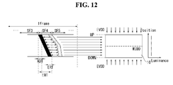
- FIG. 12 shows an example where an erase speed and a writing speed in a specific compensation subframe are differently adjusted, and an erase speed in a portion of the specific compensation subframe is different from an erase speed in a remaining portion, as a method for minimizing the luminance deviation resulting from the IR drop.
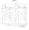
- FIG. 13 shows that application times of erase signals in the specific compensation subframe are differently controlled depending on portions divided from the specific compensation subframe, so as to implement the method shown in FIG. 12 .
- an organic light emitting diode display including: a display panel including a plurality of pixels; a display panel driver configured to drive signal lines of the display panel; and a timing controller configured to divide one frame into a plurality of subframes, divide data of an input image at each bit, map the data of the input image to the plurality of subframes, control an operation of the display panel driver, and differently adjust a writing speed for writing data and an erase speed for turning off the pixels in at least one compensation frame of the plurality of subframes.
- an erase speed for turning off the pixels is determined based on a luminance deviation depending on a position of the display panel in the compensation subframe.
Landscapes
- Engineering & Computer Science (AREA)
- Physics & Mathematics (AREA)
- Computer Hardware Design (AREA)
- General Physics & Mathematics (AREA)
- Theoretical Computer Science (AREA)
- Manufacturing & Machinery (AREA)
- Control Of Indicators Other Than Cathode Ray Tubes (AREA)
- Control Of El Displays (AREA)
Abstract
Description
- This application claims the benefit of Korea Patent Application No.
10-2014-0194442 filed on December 30, 2014 - The present disclosure relates to an organic light emitting diode display driven through a digital driving method and a method for driving the same.
- Because an organic light emitting diode display (hereinafter, referred to as "OLED display") is a self-emission display device, the OLED display may be manufactured to have lower power consumption and thinner profile than a liquid crystal display requiring a backlight unit. Further, the OLED display has advantages of a wide viewing angle and a fast response time and thus has expanded its market while competing with the liquid crystal display.
- The OLED display is driven through an analog voltage driving method or a digital driving method and may represent grayscale of an input image. The analog voltage driving method adjusts a data voltage applied to pixels based on data gray values of the input image and adjusts a luminance of the pixels based on a magnitude of the data voltage, thereby representing grayscale of the input image. The digital driving method adjusts an emission time of the pixels based on the data gray values of the input image, thereby representing grayscale of the input image.
- As shown in
FIGS. 1 and 2 , the digital driving method time-divides one frame into a plurality of subframes SF1 to SF6. Each subframe represents one bit of input image data. As shown inFIG. 1 , each subframe may include a writing time ADT, during which data is written on pixels, and an emission time EMT, during which the pixels emit light. As shown inFIG. 2 , each subframe may further include an erase time ERT, during which the pixels are turned off, in addition to the writing time ADT and the emission time EMT. The emission times of the subframes may have different lengths. However, all of the subframes are the same as one another in a scan direction for writing the data and an erase direction for turning off the pixels, and a writing speed for writing the data and an erase speed for turning off the pixels in each subframe are the same as each other. Therefore, the emission time of the same subframe is uniform irrespective of a position of the display panel. - Because the emission time of the same subframe is uniform, it is a matter of course that there is no luminance deviation irrespective of the position of the display panel. However, in fact, as shown in
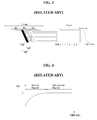
FIG. 3 , because IR drop resulting from a line resistance is generated in the display panel, a high potential power voltage EVDD varies depending on a spatial position of the display panel to thereby generate the luminance deviation. The luminance implemented in the display panel decreases as the display panel is far from an input terminal of the high potential power voltage EVDD. - In the analog voltage driving method, a driving thin film transistor (TFT) is driven in a saturation region. As shown in
FIG. 4 , the saturation region indicates a voltage region, in which a drain-source current Ids does not substantially change depending on a drain-source voltage Vds of the driving TFT, and is positioned on the right side of the Vds-Ids plane. In other words, in the saturation region, the drain-source current Ids does not change although the high potential power voltage EVDD (i.e., the drain-source voltage Vds of the driving TFT) changes. - On the other hand, in the digital driving method, the driving TFT is driven in an active region, so as to reduce power consumption. As shown in
FIG. 4 , the active region indicates a voltage region, in which the drain-source current Ids changes depending on the drain-source voltage Vds of the driving TFT, and is positioned on the left side of the Vds-Ids plane. In other words, in the active region, the drain-source current Ids sensitively changes depending on changes in the high potential power voltage EVDD (i.e., the drain-source voltage Vds of the driving TFT). - For this reason, the luminance deviation resulting from the IR drop is more of a problem in the digital driving method than the analog voltage driving method.
- Accordingly, the present disclosure provides an organic light emitting diode display driven through a digital driving method and a method for driving the same capable of minimizing a luminance deviation resulting from IR drop. Aspects of an invention are defined in the appended independent claims.
- There is provided an organic light emitting diode display comprising a display panel including a plurality of pixels; a display panel driver configured to drive signal lines of the display panel; and a timing controller configured to divide one frame into a plurality of subframes, divide data of an input image at each bit, map the data of the input image to the plurality of subframes, control an operation of the display panel driver, and differently adjust a writing speed for writing data and an erase speed for turning off the pixels in at least one compensation frame of the plurality of subframes.
- There is further provided a method for driving an organic light emitting diode display including a display panel including a plurality of pixels and a display panel driver driving signal lines of the display panel, the method comprising dividing one frame into a plurality of subframes, dividing data of an input image at each bit, and mapping the data of the input image to the plurality of subframes; and controlling an operation of the display panel driver and differently adjusting a writing speed for writing data and an erase speed for turning off the pixels in at least one compensation frame of the plurality of subframes.
- The accompanying drawings, which are included to provide a further understanding of the present disclosure and are incorporated in and constitute a part of this specification. The drawings illustrate embodiments and together with the description serve to explain the principles of the present disclosure. In the drawings:
-
FIGS. 1 and 2 illustrate a related art digital driving method; -
FIG. 3 shows that a luminance deviation resulting from IR drop is generated depending on a position of a display panel; -
FIG. 4 shows a graph indicating operating characteristics of a driving thin film transistor (TFT); -
FIGS. 5 and6 show an organic light emitting diode display according to an exemplary embodiment of the invention; -
FIG. 7 is a circuit diagram showing one pixel of the organic light emitting diode display shown inFIG. 6 ; -
FIG. 8 shows an example where an erase speed and a writing speed in a specific compensation subframe are differently adjusted as a method for minimizing a luminance deviation resulting from IR drop; -
FIG. 9 shows that a total application time of scan signals and a total application time of erase signals in the specific compensation subframe are differently controlled so as to implement the method shown inFIG. 8 ; -
FIG. 10 shows another example where an erase speed and a writing speed in a specific compensation subframe are differently adjusted as a method for minimizing a luminance deviation resulting from IR drop; -
FIG. 11 shows that a total application time of scan signals and a total application time of erase signals in the specific compensation subframe are differently controlled so as to implement the method shown inFIG. 10 ; -
FIG. 12 shows an example where an erase speed and a writing speed in a specific compensation subframe are differently adjusted, and an erase speed of a portion of the specific compensation subframe is different from an erase speed of a remaining portion, as a method for minimizing a luminance deviation resulting from IR drop; -
FIG. 13 shows that application times of erase signals in the specific compensation subframe are differently controlled depending on portions divided from the specific compensation subframe, so as to implement the method shown inFIG. 12 ; -
FIG. 14 shows an example where a scanning direction and an erase direction in a specific compensation subframe are reversely adjusted as another method for minimizing a luminance deviation resulting from IR drop; -
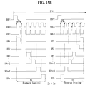
FIGS. 15A to 15C show examples where an erase speed in a compensation subframe is differently controlled depending on a degree of IR drop; and -
FIGS. 16 and 17 show a comparison between a simulation result according to an embodiment and a related art. - Reference will now be made in detail to embodiments, examples of which are illustrated in the accompanying drawings. Wherever possible, the like reference numbers will be used throughout the drawings to refer to the like parts. It will be paid attention that detailed description of known arts will be omitted if it is determined that the arts may mislead.
-
FIGS. 5 to 7 show an organic light emitting diode display (hereinafter, referred to as "OLED display") according to an embodiment. - Referring to
FIGS. 5 to 7 , the OLED display according to an embodiment includes adisplay panel 10,display panel drivers display panel 10, and atiming controller 11 for controlling thedisplay panel drivers - On the pixel array of the
display panel 10, a plurality ofdata lines 15 and a plurality of first andsecond gate lines display panel 10 includes pixels PIX, that are arranged in a matrix form and display the input image. Each pixel PIX may be one of a red (R) pixel, a green (G) pixel, a blue (B) pixel, and a white (W) pixel. As shown inFIG. 7 , each pixel PIX may include a plurality of thin film transistors (TFTs), an organic light emitting diode (OLED), a capacitor, and the like. - The
display panel drivers data driver 12, and first andsecond gate drivers - The
data driver 12 generates a data voltage SVdata based on data RGB of the input image received from thetiming controller 11 and outputs the data voltage SVdata to thedata lines 15. In a digital driving method, an amount of light emitted by the pixels PIX is uniform, and grayscale of the data RGB is represented through an amount of emission time, during which the pixels PIX emit light. Therefore, thedata driver 12 selects one of a voltage (hereinafter, referred to as "on-voltage") satisfying an emission condition of the pixels PIX and a voltage (hereinafter, referred to as "off-voltage") not satisfying the emission condition of the pixels PIX depending on digital values of the data RGB mapped to the subframe and generates the data voltage SVdata. - The
first gate driver 13 sequentially supplies a scan pulse (or a gate pulse) SP synchronized with the data voltage SVdata of thedata driver 12 to the first gate lines 16 (i.e., 161 to 16n) under the control of thetiming controller 11. Thefirst gate driver 13 sequentially shifts the scan pulse SP and sequentially selects the pixels PIX, to which the data voltage SVdata is applied, on a per line basis. - The
second gate driver 14 sequentially supplies an erase pulse EP to the second gate lines 17 (i.e., 171 to 17n) under the control of thetiming controller 11. The pixels PIX stop emitting light in response to the erase pulse EP. Thetiming controller 11 controls application timing of the erase pulse EP and controls an emission time of each subframe. - The
timing controller 11 receives the pixel data RGB of the input image and timing signals synchronized with the pixel data RGB from a host system (not shown). Thetiming controller 11 controls operation timing of thedata driver 12 and operation timing of thegate drivers timing controller 11 generates a source timing control signal DDC controlling the operation timing of thedata driver 12, a first gate timing control signal GDC controlling the operation timing of thefirst gate driver 13, and a second gate timing control signal EDC controlling the operation timing of thesecond gate driver 14. - The
timing controller 11 controls thedisplay panel drivers timing controller 11 divides one frame into a plurality of subframes. Lengths of the emission times of the subframes may be differently set depending on a data bit of the input image. For example, the most significant bit (MSB) represents a high gray level and thus may be mapped to the subframe having the long emission time, and the least significant bit (LSB) represents a low gray level and thus may be mapped to the subframe having the small emission time. Thetiming controller 11 maps the data RGB of the input image to the subframe at each bit and transmits the data RGB to thedata driver 12. - As shown in
FIGS. 8 ,10 ,12 , and14 , each subframe may further include an erase time ERT, during which the pixels PIX are turned off, as well as a writing time ADT, during which the data is written on the pixels PIX, and an emission time EMT, during which the pixels PIX emit light. As described above, the emission times EMT of the subframes may have different lengths. - The
timing controller 11 controls operations of thedisplay panel drivers timing controller 11 differently adjusts emission times of upper and lower display lines of thedisplay panel 10 and can suppress a luminance deviation resulting from IR drop depending on a position of thedisplay panel 10. This is described in detail later with reference toFIGS. 8 to 13 . - The
timing controller 11 controls the operations of thedisplay panel drivers timing controller 11 differently adjusts emission times of the upper and lower display lines of thedisplay panel 10 and can suppress the luminance deviation resulting from the IR drop depending on the position of thedisplay panel 10. This is described in detail later with reference toFIGS. 14 to 15C . - The host system may be implemented as one of a television system, a set-top box, a navigation system, a DVD player, a Blu-ray player, a personal computer (PC), a home theater system, and a phone system.
- As shown in
FIG. 7 , each pixel PIX includes an OLED, a driving TFT DT, a first switching TFT ST1, a second switching TFT ST2, a storage capacitor Cst, and the like. - The OLED has a stack structure of organic compound layers including a hole injection layer HIL, a hole transport layer HTL, an emission layer EML, an electron transport layer ETL, an electron injection layer EIL, etc. The OLED generates light when electrons and holes combine in the emission layer EML.
- The driving TFT DT operates in the active region shown in
FIG. 4 and makes the OLED emit light. The driving TFT DT is connected between a power line, to which a high potential power voltage EVDD is supplied, and the OLED and switches on or off a current flowing in the OLED depending on a voltage state of a gate node Ng. The driving TFT DT is turned on when the gate node Ng is in an on-voltage state, and applies a driving current to the OLED, thereby making the OLED emit light. The driving TFT DT is turned off when the gate node Ng is in an off-voltage state, and cuts off the driving current applied to the OLED, thereby turning off the OLED. Namely, the OLED does not emit light. - The first switching TFT ST1 is turned on in response to the scan pulse SP from the
first gate line 16. The first switching TFT ST1 supplies the data voltage SVdata of the on-voltage or the off-voltage to the gate node Ng in response to the scan pulse SP. - The second switching TFT ST2 is turned on in response to the erase pulse EP from the
second gate line 17. The second switching TFT ST2 makes a voltage of the gate node Ng in an off-voltage state in response to the erase pulse EP. - The storage capacitor Cst maintains the voltage of the gate node Ng of the driving TFT DT.
- Each pixel PIX of the
display panel 10 according to an embodiment is not limited to the structure shown inFIG. 7 and may have any pixel structure capable of performing the digital driving method. -
FIG. 8 shows an example where an erase speed and a writing speed in a specific compensation subframe are differently adjusted as a method for minimizing the luminance deviation resulting from the IR drop.FIG. 9 shows that a total application time of the scan signals and a total application time of the erase signals in the specific compensation subframe are differently controlled so as to implement the method shown inFIG. 8 . - As shown in
FIG. 8 , in the OLED display according to an embodiment, the high potential power voltage EVDD for driving the pixels is applied to thedisplay panel 10 from the upper side UP of thedisplay panel 10, and the data write may be sequentially performed from the upper side UP to the lower side DOWN of thedisplay panel 10 in a sequential line manner. In this instance, a luminance at the lower side DOWN of thedisplay panel 10 may be less than a luminance at the upper side UP of thedisplay panel 10 because of the IR drop. - To remove the luminance deviation depending on the position of the
display panel 10, thetiming controller 11 controls the operations of thedisplay panel drivers display panel 10, the emission time EMT may gradually increase. - The writing speed is determined in inverse proportion to a total application time of the scan signals for writing the data in the compensation subframe SF4, and the erase speed is determined in inverse proportion to a total application time of the erase signals for turning off the pixels in the compensation subframe SF4.
- As shown in
FIG. 9 , thetiming controller 11 may cause a total application time Te of erase signals EP1 to EPn to be longer than a total application time Ts of scan signals SP1 to SPn, so that the erase speed is slower than the writing speed in the compensation subframe SF4. For this, thetiming controller 11 may cause a first gate shift clock GSC1, that forms the basis of the generation of the scan signals SP1 to SPn, to have a first pulse period P1 and cause a second gate shift clock GSC2, that forms the basis of the generation of the erase signals EP1 to EPn, to have a second pulse period P2 longer than the first pulse period P1. - The
first gate driver 13 receives the first gate shift clock GSC1, a first gate start pulse GSP1, and a first gate output enable signal GOE1 from thetiming controller 11 and generates the scan signals SP1 to SPn in synchronization with a rising edge of the first gate shift clock GSC1. Thefirst gate driver 13 sequentially supplies the scan signals SP1 to SPn to thefirst gate lines 16 and scans the display lines of thedisplay panel 10 in a forward direction during the total scanning time Ts. - The
second gate driver 14 receives the second gate shift clock GSC2, a second gate start pulse GSP2, and a second gate output enable signal GOE2 from thetiming controller 11 and generates the erase signals EP1 to EPn in synchronization with a rising edge of the second gate shift clock GSC2. Thesecond gate driver 14 sequentially supplies the erase signals EP1 to EPn to thesecond gate lines 17 and erases the display lines of thedisplay panel 10 in the forward direction during the total erase time Te longer than the total scanning time Ts. - As described above, this causes the erase speed to be slower than the writing speed when the high potential power voltage EVDD is applied to the
display panel 10 from the upper side UP of thedisplay panel 10 as shown inFIG. 8 , and gradually increases the emission time EMT as it goes from the upper side UP to the lower side DOWN of thedisplay panel 10, thereby removing the luminance deviation resulting from the IR drop depending on the position of thedisplay panel 10. -
FIG. 10 shows another example where an erase speed and a writing speed in a specific compensation subframe are differently adjusted as a method for minimizing the luminance deviation resulting from the IR drop.FIG. 11 shows that a total application time of the scan signals and a total application time of the erase signals in the specific compensation subframe are differently controlled so as to implement the method shown inFIG. 10 . - As shown in
FIG. 10 , in the OLED display according to a further embodiment, the high potential power voltage EVDD for driving the pixels is applied to thedisplay panel 10 from the lower side DOWN of thedisplay panel 10, and the data write may be sequentially performed from the upper side UP to the lower side DOWN of thedisplay panel 10 in the sequential line manner. In this instance, a luminance at the upper side UP of thedisplay panel 10 may be less than a luminance at the lower side DOWN of thedisplay panel 10 because of the IR drop. - To remove the luminance deviation depending on the position of the
display panel 10, thetiming controller 11 controls the operations of thedisplay panel drivers display panel 10, the emission time EMT may gradually increase. - As shown in
FIG. 11 , thetiming controller 11 may cause a total application time Te of the erase signals EP1 to EPn to be shorter than a total application time Ts of the scan signals SP1 to SPn, so that the erase speed is faster than the writing speed in the compensation subframe SF4. For this, thetiming controller 11 may cause a first gate shift clock GSC1, that forms the basis of the generation of the scan signals SP1 to SPn, to have a first pulse period P1 and cause a second gate shift clock GSC2, that forms the basis of the generation of the erase signals EP1 to EPn, to have a second pulse period P2 shorter than the first pulse period P1. - The
first gate driver 13 receives the first gate shift clock GSC1, a first gate start pulse GSP1, and a first gate output enable signal GOE1 from thetiming controller 11 and generates the scan signals SP1 to SPn in synchronization with a rising edge of the first gate shift clock GSC1. Thefirst gate driver 13 sequentially supplies the scan signals SP1 to SPn to thefirst gate lines 16 and scans the display lines of thedisplay panel 10 in the forward direction during the total scanning time Ts. - The
second gate driver 14 receives the second gate shift clock GSC2, a second gate start pulse GSP2, and a second gate output enable signal GOE2 from thetiming controller 11 and generates the erase signals EP1 to EPn in synchronization with a rising edge of the second gate shift clock GSC2. Thesecond gate driver 14 sequentially supplies the erase signals EP1 to EPn to thesecond gate lines 17 and erases the display lines of thedisplay panel 10 in the forward direction during the total erase time Te shorter than the total scanning time Ts. - As described above, this causes the erase speed to be faster than the writing speed when the high potential power voltage EVDD is applied to the
display panel 10 from the lower side DOWN of thedisplay panel 10 as shown inFIG. 10 , and gradually increases the emission time EMT as it goes from the lower side DOWN to the upper side UP of thedisplay panel 10, thereby removing the luminance deviation resulting from the IR drop depending on the position of thedisplay panel 10. -
FIG. 12 shows an example where an erase speed and a writing speed in a specific compensation subframe are differently adjusted, and an erase speed in a portion of the specific compensation subframe is different from an erase speed in a remaining portion, as a method for minimizing the luminance deviation resulting from the IR drop.FIG. 13 shows that application times of erase signals in the specific compensation subframe are differently controlled depending on portions divided from the specific compensation subframe, so as to implement the method shown inFIG. 12 . - As shown in
FIG. 12 , in the OLED display according to a yet further embodiment, the high potential power voltage EVDD for driving the pixels is simultaneously applied to thedisplay panel 10 from both the upper side UP and the lower side DOWN of thedisplay panel 10, and the data write may be sequentially performed from the upper side UP and the lower side DOWN of thedisplay panel 10 in the sequential line manner. In this instance, a luminance at the middle part MIDD of thedisplay panel 10 may be less than a luminance at the upper side UP and the lower side DOWN of thedisplay panel 10 because of the IR drop. - To remove the luminance deviation depending on the position of the
display panel 10, thetiming controller 11 controls the operations of thedisplay panel drivers display panel 10 and from the lower side DOWN to the middle part MIDD of thedisplay panel 10, the emission time EMT may gradually increase. - The erase signals EP1 to EPn include first erase signals EP1 to EPk applied in the portion of the compensation subframe SF4 and second erase signals EP(k+1) to EPn applied in the remaining portion of the compensation subframe SF4. In this instance, as shown in
FIG. 13 , thetiming controller 11 may cause a total application time Te of the erase signals EP1 to EPn to be same as a total application time Ts of the scan signals SP1 to SPn, divide the total application time Te of the erase signals EP1 to EPn into a first erase time Te1, during which the first erase signals EP1 to EPk are applied, and a second erase time Te2, during which the second erase signals EP(k+1) to EPn are applied, and cause the first erase time Te1 to be longer than the second erase time Te2, so as to differently adjust the erase speed depending on the portions divided from the compensation subframe SF4. - For this, the
timing controller 11 may cause a first gate shift clock GSC1, that forms the basis of the generation of the scan signals SP1 to SPn, to have a first pulse period P1 and cause a second gate shift clock GSC2, that forms the basis of the generation of the erase signals EP1 to EPn, to have a second pulse period P2 longer than the first pulse period P1 during the first erase time Te1 and to have a third pulse period P3 shorter than the first pulse period P1 during the second erase time Te2. - The
first gate driver 13 receives the first gate shift clock GSC1, a first gate start pulse GSP1, and a first gate output enable signal GOE1 from thetiming controller 11 and generates the scan signals SP1 to SPn in synchronization with a rising edge of the first gate shift clock GSC1. Thefirst gate driver 13 sequentially supplies the scan signals SP1 to SPn to thefirst gate lines 16 and scans the display lines of thedisplay panel 10 in the forward direction during the total scanning time Ts. - The
second gate driver 14 receives the second gate shift clock GSC2, a second gate start pulse GSP2, and a second gate output enable signal GOE2 from thetiming controller 11 and generates the erase signals EP1 to EPn in synchronization with a rising edge of the second gate shift clock GSC2. Thesecond gate driver 14 sequentially supplies the erase signals EP1 to EPn to thesecond gate lines 17 and erases the display lines of thedisplay panel 10 in the forward direction at a first erase speed slower than the writing speed during the first erase time Te1 and at a second erase speed faster than the writing speed during the second erase time Te2. - As described above, thisdifferently adjusts the erase speed depending on the portions divided from the compensation subframe (i.e., causes the erase speed to be slower than the writing speed in the portion of the compensation subframe and to be faster than the writing speed in the remaining portion of the compensation subframe) when the high potential power voltage EVDD is simultaneously applied to the
display panel 10 from both the upper side UP and the lower side DOWN of thedisplay panel 10 as shown inFIG. 12 . Hence, the embodiment of the invention gradually increases the emission time EMT as it goes from the upper side UP and the lower side DOWN to the middle part MIDD of thedisplay panel 10, thereby removing the luminance deviation resulting from the IR drop depending on the position of thedisplay panel 10. -
FIG. 14 shows an example where a scanning direction and an erase direction in a specific compensation subframe are reversely adjusted as another method for minimizing the luminance deviation resulting from the IR drop.FIGS. 15A to 15C show examples where an erase speed in a compensation subframe is differently controlled depending on a degree of the IR drop. - As shown in
FIG. 14 , in the OLED display according to a still further embodiment, the high potential power voltage EVDD for driving the pixels is applied to thedisplay panel 10 from the lower side DOWN of thedisplay panel 10, and the data write may be sequentially performed from the upper side UP to the lower side DOWN of thedisplay panel 10 in the sequential line manner. In this instance, a luminance at the upper side UP of thedisplay panel 10 may be less than a luminance at the lower side DOWN of thedisplay panel 10 because of the IR drop. - To remove the luminance deviation depending on the position of the
display panel 10, thetiming controller 11 controls the operations of thedisplay panel drivers timing controller 11 may define the scanning direction as a forward direction and define the erase direction as a reverse direction. Hence, thetiming controller 11 can gradually increase the emission time EMT as it goes from the lower side DOWN to the upper side UP of thedisplay panel 10. - The erase speed of the reverse direction may be differently determined depending on a degree of the luminance deviation resulting from the IR drop on the upper and lower sides of the
display panel 10. - When the luminance deviation is large, the
timing controller 11 may cause the erase speed of the reverse direction to be slower than the writing speed of the forward direction in the compensation subframe SF4. For this, as shown inFIG. 15A , thetiming controller 11 may cause a total application time Te of the erase signals EP1 to EPn to be longer than a total application time Ts of the scan signals SP1 to SPn. Thetiming controller 11 may cause a first gate shift clock GSC1, that forms the basis of the generation of the scan signals SP1 to SPn, to have a first pulse period P1 and may cause a second gate shift clock GSC2, that forms the basis of the generation of the erase signals EP1 to EPn, to have a second pulse period P2 longer than the first pulse period P1. Thefirst gate driver 13 sequentially supplies the scan signals SP1 to SPn to thefirst gate lines 16 in the forward direction and scans the display lines of thedisplay panel 10 in the forward direction during the total scanning time Ts. Thesecond gate driver 14 sequentially supplies the erase signals EP1 to EPn to thesecond gate lines 17 in the reverse direction and erases the display lines of thedisplay panel 10 in the reverse direction during the total erase time Te longer than the total scanning time Ts. - On the contrary, when the luminance deviation is small, the
timing controller 11 may cause the erase speed of the reverse direction to be faster than the writing speed of the forward direction in the compensation subframe SF4. For this, as shown inFIG. 15B , thetiming controller 11 may cause a total application time Te of the erase signals EP1 to EPn to be shorter than a total application time Ts of the scan signals SP1 to SPn. Thetiming controller 11 may cause the first gate shift clock GSC1, that forms the basis of the generation of the scan signals SP1 to SPn, to have the first pulse period P1 and may cause the second gate shift clock GSC2, that forms the basis of the generation of the erase signals EP1 to EPn, to have the second pulse period P2 shorter than the first pulse period P1. Thefirst gate driver 13 sequentially supplies the scan signals SP1 to SPn to thefirst gate lines 16 in the forward direction and scans the display lines of thedisplay panel 10 in the forward direction during the total scanning time Ts. Thesecond gate driver 14 sequentially supplies the erase signals EP1 to EPn to thesecond gate lines 17 in the reverse direction and erases the display lines of thedisplay panel 10 in the reverse direction during the total erase time Te shorter than the total scanning time Ts. - Alternatively, as shown in
FIG. 15C , when the luminance deviation is small, thetiming controller 11 may cause the erase speed of the reverse direction to be same as the writing speed of the forward direction in the compensation subframe SF4. -
FIGS. 16 and 17 show a comparison between a simulation result according to an embodiment and a related art. - The present applicant adopted one configuration according to the embodiment shown in
FIG. 8 and then measured luminances depending on the position of the display panel. Referring toFIG. 16 , an increase in a value of a vertical line indicates that the position of the display panel is close to the lower side of the display panel. - As can be seen from the simulation result of
FIGS. 16 and 17 , the embodiment of the invention greatly reduced a deviation between the luminances of the upper and lower sides of the display panel, compared to the related art. - As described above, this selects at least one of the plurality of subframes belonging to one frame as the compensation subframe and causes the erase speed for turning off the pixels to be faster or slower than the writing speed for the data write in the compensation subframe, thereby differently controlling the emission times of the upper and lower display lines of the display panel. This can minimize the luminance deviation resulting from the IR drop.
- Furthermore, this embodiment selects at least one of the plurality of subframes belonging to one frame as the compensation subframe and reversely controls the scanning direction for the data write and the erase direction for turning off the pixels in the compensation subframe, thereby differently controlling the emission times of the upper and lower display lines of the display panel. This can minimize the luminance deviation resulting from the IR drop.
- Although embodiments have been described with reference to a number of illustrative embodiments thereof, it should be understood that numerous other modifications and embodiments can be devised by those skilled in the art that will fall within the scope of the principles of the present disclosure. More particularly, various variations and modifications are possible in the component parts and/or arrangements of the subject combination arrangement within the scope of the disclosure, the drawings and the appended claims. In addition to variations and modifications in the component parts and/or arrangements, alternative uses will also be apparent to those skilled in the art.
- There is also provided an organic light emitting diode display including: a display panel including a plurality of pixels; a display panel driver configured to drive signal lines of the display panel; and a timing controller configured to divide one frame into a plurality of subframes, divide data of an input image at each bit, map the data of the input image to the plurality of subframes, control an operation of the display panel driver, and differently adjust a writing speed for writing data and an erase speed for turning off the pixels in at least one compensation frame of the plurality of subframes.
- Optionally, when a high potential power voltage for driving the pixels is applied to the display panel from an upper side of the display panel, and the data write is sequentially performed from the upper side of the display panel to a lower side of the display panel opposite the upper side in a sequential line manner, the timing controller controls an operation of the display panel driver such that the erase speed is slower than the writing speed in the compensation subframe.
- Optionally, the timing controller controls a total application time of erase signals for turning off the pixels to be longer than a total application time of scan signals for writing the data in the compensation subframe, and the timing controller controls a first gate shift clock, that forms the basis of the generation of the scan signals, to have a first pulse period and controls a second gate shift clock, that forms the basis of the generation of the erase signals, to have a second pulse period longer than the first pulse period.
- Optionally, when a high potential power voltage for driving the pixels is applied to the display panel from a lower side of the display panel, and the data write is sequentially performed from an upper side opposite the lower side of the display panel to the lower side of the display panel in a sequential line manner, the timing controller controls an operation of the display panel driver such that the erase speed is faster than the writing speed in the compensation subframe.
- Optionally, the timing controller controls a total application time of erase signals for turning off the pixels to be shorter than a total application time of scan signals for writing the data in the compensation subframe, and the timing controller controls a first gate shift clock, that forms the basis of the generation of the scan signals, to have a first pulse period and controls a second gate shift clock, that forms the basis of the generation of the erase signals, to have a second pulse period shorter than the first pulse period.
- Optionally, when a high potential power voltage for driving the pixels is applied to the display panel from an upper side and a lower side of the display panel that are opposite to each other, and the data write is sequentially performed from the upper side to the lower side of the display panel in a sequential line manner, the timing controller controls an operation of the display panel driver such that the erase speed is slower than the writing speed in a portion of the compensation subframe, and then the erase speed is faster than the writing speed in a remaining portion of the compensation subframe.
- Optionally erase signals for turning off the pixels include first erase signals applied in the portion of the compensation subframe and second erase signals applied in the remaining portion of the compensation subframe, and the timing controller controls a total application time of the erase signals to be same as a total application time of scan signals for writing the data in the compensation subframe, divides the total application time of the erase signals into a first erase time, during which the first erase signals are applied, and a second erase time, during which the second erase signals are applied, and controls the first erase time to be longer than the second erase time, and the timing controller controls a first gate shift clock, that forms the basis of the generation of the scan signals, to have a first pulse period and controls a second gate shift clock, that forms the basis of the generation of the erase signals, to have a second pulse period longer than the first pulse period during the first erase time and to have a third pulse period shorter than the first pulse period during the second erase time.
- Optionally, the timing controller reversely adjusts a scanning direction for writing the data and an erase direction for turning off the pixels in the compensation subframe.
- Optionally, an erase speed for turning off the pixels is determined based on a luminance deviation depending on a position of the display panel in the compensation subframe.
- Optionally, each of the plurality of subframes includes a writing time during which the data is written on the pixels, an emission time during which the pixels emit light, and an erase time during which the pixels are turned off.
- There is also provided a method for driving an organic light emitting diode display including a display panel including a plurality of pixels and a display panel driver driving signal lines of the display panel, the method including: dividing one frame into a plurality of subframes, dividing data of an input image at each bit, and mapping the data of the input image to the plurality of subframes; and controlling an operation of the display panel driver and differently adjusting a writing speed for writing data and an erase speed for turning off the pixels in at least one compensation frame of the plurality of subframes.
- Optionally the method further includes reversely adjusting a scanning direction for writing the data and an erase direction for turning off the pixels in the compensation subframe.
- Optionally, an erase speed for turning off the pixels is determined based on a luminance deviation depending on a position of the display panel in the compensation subframe.
- Optionally, each of the plurality of subframes includes a writing time during which the data is written on the pixels, an emission time during which the pixels emit light, and an erase time during which the pixels are turned off.
Claims (15)
- An organic light emitting diode display comprising:a display panel (10) including a plurality of pixels;a display panel driver (12, 13, 14) configured to drive signal lines of the display panel (10); anda timing controller (11) configured to:divide one frame into a plurality of subframes;convert data of an input image into a bit pattern;map the bit pattern to the plurality of subframes;control an operation of the display panel driver (12, 13, 14); andadjust a writing speed for writing data and/or an erase speed for turning off pixels of the plurality of pixels in at least one compensation subframe (SF4) of the plurality of subframes such that the write speed and the erase speed are different from each other.
- The organic light emitting diode display according to claim 1, wherein when a high potential power voltage for driving the plurality of pixels is applied to the display panel (10) from a first side of the display panel (10), and writing data is sequentially performed from the first side of the display panel (10) to a second side of the display panel (10) opposite the first side sequentially in a line-by-line manner, the timing controller (11) is configured to control an operation of the display panel driver (12, 13, 14) such that the erase speed is slower than the writing speed in the at least one compensation subframe (SF4).
- The organic light emitting diode display according to claim 1 or 2, wherein the timing controller (11) is further configured to control a total application time of erase signals (EP1 to EPn) for turning off the plurality of pixels to be longer than a total application time of scan signals (SP1 to SPn) for writing the data in the at least one compensation subframe (SF4), and
wherein the timing controller (11) is also configured to:control a first gate shift clock (GSC1), that forms the basis of the generation of the scan signals (SP1 to SPn), to have a first pulse period (P1); andcontrol a second gate shift clock (GSC2), that forms the basis of the generation of the erase signals (EP1 to EPn), to have a second pulse period (P2) longer than the first pulse period (P1). - The organic light emitting diode display according to claim 1, wherein, when a high potential power voltage for driving the plurality of pixels is applied to the display panel (10) from a second side of the display panel (10), and writing data is sequentially performed from a first side opposite the second side of the display panel (10) to the second side of the display panel (10) sequentially in a line-by-line manner, the timing controller (11) is configured to control an operation of the display panel driver (12, 13, 14) such that the erase speed is faster than the writing speed in the at least one compensation subframe (SF4).
- The organic light emitting diode display according to claim 4, wherein the timing controller (11) is further configured to control a total application time of erase signals (EP1 to EPn) for turning off the plurality of pixels to be shorter than a total application time of scan signals (SP1 to SPn) for writing the data in the at least one compensation subframe (SF4), and
wherein the timing controller (11) is also configured to:control a first gate shift clock (GSC1), that forms the basis of the generation of the scan signals (SP1 to SPn), to have a first pulse period (P1); andcontrol a second gate shift clock (GCS2), that forms the basis of the generation of the erase signals (EP1 to EPn), to have a second pulse period (P2) shorter than the first pulse period (P1). - The organic light emitting diode display according to claim 1, wherein, when a high potential power voltage for driving the plurality of pixels is applied to the display panel (10) from a firstside and a second side of the display panel (10) that are opposite to each other, and writing data is sequentially performed from the first side to the second side of the display panel (10) sequentially in a line-by-line manner, the timing controller (11) is configured to control an operation of the display panel driver (12, 13, 14) such that the erase speed is slower than the writing speed in a portion of the at least one compensation subframe (SF4), and the erase speed is faster than the writing speed in a remaining portion of the at least one compensation subframe (SF4).
- The organic light emitting diode display according to claim 6, wherein erase signals (EP1 to EPn) for turning off the plurality of pixels include first erase signals (EP1 to EPk) applied in the portion of the at least one compensation subframe (SF4) and second erase signals (EPk+1 to EPn) applied in the remaining portion of the at least one compensation subframe (SF4),
wherein the timing controller (11) is further configured to:control a total application time of the erase signals (EP1 to EPn) to be same as a total application time of scan signals (SP1 to SPn) for writing the data in the at least one compensation subframe (SF4);divide the total application time of the erase signals (EP1 to EPn) into a first erase time (Te1), during which the first erase signals (EP1 to EPk) are applied, and a second erase time (Te2), during which the second erase signals (EPk+1 to EPn) are applied; andcontrol the first erase time (Te1) to be longer than the second erase time (Te2), andwherein the timing controller (11) is also configured to:control a first gate shift clock (GSC1) to have a first pulse period (P1), that forms the basis of the generation of the scan signals (SP1 to SPn); andcontrol a second gate shift clock (GSC2) to have a second pulse period (P2) longer than the first pulse period (P1) during the first erase time (Te1) and to have a third pulse period (P3) shorter than the first pulse period (P1) during the second erase time (Te2),wherein the first gate shift clock (GSC1) and second gate shift clock (GSC2) form the basis of the generation of the scan signals (SP1 to SPn) and the erase signals (EP1 to EPn), respectively. - The organic light emitting diode display according to any preceding claim, wherein the timing controller (11) is configured to reverse a scanning direction for writing the data and/or an erase direction for turning off pixels of the plurality of pixels in the at least one compensation subframe (SF4).
- The organic light emitting diode display according to any preceding claim, wherein an erase speed for turning off pixels of the plurality of pixels is determined based on a luminance deviation depending on a position on the display panel (10) in the at least one compensation subframe (SF4).
- The organic light emitting diode display according to any one of claims 1 to 9, wherein each of the plurality of subframes includes a writing time (ADT) during which the data is written to pixels of the plurality of pixels, an emission time (EMT) during which the pixels emit light, and an erase time (ERT) during which the pixels are turned off.
- A method for driving an organic light emitting diode display including a display panel (10) including a plurality of pixels and a display panel driver (12, 13, 14) driving signal lines of the display panel, the method comprising:dividing one frame into a plurality of subframes;converting data of an input image into a bit pattern;mapping the bit pattern to the plurality of subframes; andadjusting a writing speed for writing data and/or an erase speed for turning off pixels of the plurality of pixels in at least one compensation subframe (SF4) of the plurality of subframes, such that the write speed and the erase speed are different from each other.
- The method according to claim 11, further comprising reversing a scanning direction for writing the data and/or an erase direction for turning off pixels of the plurality of pixels in the at least one compensation subframe.
- The method according to claim 12, wherein an erase speed for turning off pixels of the plurality of pixels is determined based on a luminance deviation depending on a position on the display panel (10) in the at least one compensation subframe (SF4).
- The method according to any one of claims 11 to 13, wherein each of the plurality of subframes includes a writing time (ADT) during which the data is written to pixels of the plurality of pixels, an emission time (EMT) during which the pixels emit light, and an erase time (ERT) during which the pixels are turned off.
- The method according to claim 11 or 12, wherein a first difference between the erase speed and the write speed in a first portion of the at least one compensation subframe (SF4) is different from a second difference between the erase speed and the write speed in a second portion of the at least one compensation subframe (SF4).
Applications Claiming Priority (1)
| Application Number | Priority Date | Filing Date | Title |
|---|---|---|---|
| KR1020140194442A KR102380763B1 (en) | 2014-12-30 | 2014-12-30 | Organic light emitting display device and driving method thereof |
Publications (2)
| Publication Number | Publication Date |
|---|---|
| EP3040963A1 true EP3040963A1 (en) | 2016-07-06 |
| EP3040963B1 EP3040963B1 (en) | 2019-01-16 |
Family
ID=53524688
Family Applications (1)
| Application Number | Title | Priority Date | Filing Date |
|---|---|---|---|
| EP15175885.1A Active EP3040963B1 (en) | 2014-12-30 | 2015-07-08 | Organic light emitting diode display and method for driving the same |
Country Status (4)
| Country | Link |
|---|---|
| US (1) | US9711081B2 (en) |
| EP (1) | EP3040963B1 (en) |
| KR (1) | KR102380763B1 (en) |
| CN (1) | CN105761669B (en) |
Families Citing this family (24)
| Publication number | Priority date | Publication date | Assignee | Title |
|---|---|---|---|---|
| KR102328841B1 (en) * | 2014-12-24 | 2021-11-19 | 엘지디스플레이 주식회사 | Organic light emitting display device and driving method thereof |
| TWI564867B (en) * | 2016-03-18 | 2017-01-01 | 明陽半導體股份有限公司 | Light-emitting diode driving circuit and method |
| CN106097967A (en) * | 2016-08-25 | 2016-11-09 | 深圳市华星光电技术有限公司 | A kind of OLED PWM driving method |
| TWI622976B (en) * | 2017-03-15 | 2018-05-01 | 明陽半導體股份有限公司 | Gray scale generating circuit and driving circuit using same |
| CN110223628B (en) * | 2017-04-07 | 2021-04-23 | 合肥集创微电子科技有限公司 | LED display device and driving method thereof |
| KR102395792B1 (en) | 2017-10-18 | 2022-05-11 | 삼성디스플레이 주식회사 | Display device and driving method thereof |
| KR20200063348A (en) | 2018-11-22 | 2020-06-05 | 이미진 | Blogger and advertiser recommendation system based on bigdata collaborative filtering and method thereof |
| KR102782858B1 (en) * | 2019-02-08 | 2025-03-17 | 삼성디스플레이 주식회사 | Organic light emitting diode display device |
| US11694601B2 (en) | 2019-03-29 | 2023-07-04 | Creeled, Inc. | Active control of light emitting diodes and light emitting diode displays |
| US11790831B2 (en) | 2019-03-29 | 2023-10-17 | Creeled, Inc. | Active control of light emitting diodes and light emitting diode displays |
| US12142716B2 (en) | 2019-03-29 | 2024-11-12 | Creeled, Inc. | Active control of light emitting diodes and light emitting diode displays |
| US12198605B2 (en) | 2019-03-29 | 2025-01-14 | Creeled, Inc. | Active control of light emitting diodes and light emitting diode displays |
| US11727857B2 (en) | 2019-03-29 | 2023-08-15 | Creeled, Inc. | Active control of light emitting diodes and light emitting diode displays |
| KR102845462B1 (en) * | 2020-06-23 | 2025-08-11 | 삼성전자주식회사 | Light emitting diode package and display apparatus including the same |
| US11357087B2 (en) * | 2020-07-02 | 2022-06-07 | Solomon Systech (Shenzhen) Limited | Method for driving a passive matrix LED display |
| CN113741848B (en) * | 2021-09-15 | 2024-02-23 | Oppo广东移动通信有限公司 | Image display method, DDIC, display screen module and terminal |
| WO2023150502A1 (en) | 2022-02-07 | 2023-08-10 | Creeled, Inc. | Light-emitting diodes with mixed clock domain signaling |
| US12014673B2 (en) * | 2022-02-07 | 2024-06-18 | Creeled, Inc. | Light-emitting diodes with mixed clock domain signaling |
| KR20230125679A (en) | 2022-02-21 | 2023-08-29 | (주)리브레크리에이티브컴퍼니 | Marketing diagnosis method based on bigdata and marketing diagnosis system |
| CN114596816B (en) * | 2022-03-04 | 2023-05-12 | 武汉天马微电子有限公司 | Display panel, driving method thereof and display device |
| US12618917B2 (en) | 2022-11-15 | 2026-05-05 | Creeled, Inc. | Error detection in LED packages |
| US12014677B1 (en) | 2023-04-10 | 2024-06-18 | Creeled, Inc. | Light-emitting diode packages with transformation and shifting of pulse width modulation signals and related methods |
| US12526889B2 (en) | 2023-08-29 | 2026-01-13 | Creeled, Inc. | Light-emitting diode packages with varying current pulse width modulation and related methods |
| US12437707B2 (en) | 2023-09-27 | 2025-10-07 | Creeled, Inc. | Pseudo-exponential encoding for light-emitting devices and related methods |
Citations (3)
| Publication number | Priority date | Publication date | Assignee | Title |
|---|---|---|---|---|
| US7474282B2 (en) * | 2002-01-25 | 2009-01-06 | Sharp Kabushiki Kaisha | Display unit operating control method, display control method, and display apparatus |
| US20100188393A1 (en) * | 2006-08-07 | 2010-07-29 | Pioneer Corporation | Pixel driving apparatus and pixel driving method |
| US20120320005A1 (en) * | 2011-06-20 | 2012-12-20 | Canon Kabushiki Kaisha | Display apparatus and a method for driving the same |
Family Cites Families (4)
| Publication number | Priority date | Publication date | Assignee | Title |
|---|---|---|---|---|
| US6208325B1 (en) * | 1993-10-01 | 2001-03-27 | Cirrus Logic, Inc. | Image rotation for video displays |
| US6909419B2 (en) * | 1997-10-31 | 2005-06-21 | Kopin Corporation | Portable microdisplay system |
| JP2002207463A (en) * | 2000-11-13 | 2002-07-26 | Mitsubishi Electric Corp | Liquid crystal display |
| JP3772842B2 (en) * | 2003-03-05 | 2006-05-10 | セイコーエプソン株式会社 | Liquid crystal device, driving method thereof, and electronic apparatus |
-
2014
- 2014-12-30 KR KR1020140194442A patent/KR102380763B1/en active Active
-
2015
- 2015-07-08 EP EP15175885.1A patent/EP3040963B1/en active Active
- 2015-07-30 CN CN201510459780.0A patent/CN105761669B/en active Active
- 2015-10-12 US US14/880,898 patent/US9711081B2/en active Active
Patent Citations (3)
| Publication number | Priority date | Publication date | Assignee | Title |
|---|---|---|---|---|
| US7474282B2 (en) * | 2002-01-25 | 2009-01-06 | Sharp Kabushiki Kaisha | Display unit operating control method, display control method, and display apparatus |
| US20100188393A1 (en) * | 2006-08-07 | 2010-07-29 | Pioneer Corporation | Pixel driving apparatus and pixel driving method |
| US20120320005A1 (en) * | 2011-06-20 | 2012-12-20 | Canon Kabushiki Kaisha | Display apparatus and a method for driving the same |
Also Published As
| Publication number | Publication date |
|---|---|
| EP3040963B1 (en) | 2019-01-16 |
| CN105761669B (en) | 2019-06-25 |
| US20160189605A1 (en) | 2016-06-30 |
| CN105761669A (en) | 2016-07-13 |
| KR102380763B1 (en) | 2022-04-01 |
| US9711081B2 (en) | 2017-07-18 |
| KR20160083382A (en) | 2016-07-12 |
Similar Documents
| Publication | Publication Date | Title |
|---|---|---|
| EP3040963B1 (en) | Organic light emitting diode display and method for driving the same | |
| US10347173B2 (en) | Organic light emitting diode display and method for driving the same | |
| KR102322708B1 (en) | Organic light emitting diode display device and method of sensing device characteristic | |
| US9412304B2 (en) | Display device and method for driving the same | |
| US9672769B2 (en) | Display apparatus and method of driving the same | |
| EP3038084B1 (en) | Display device and self-calibration method thereof | |
| KR102412107B1 (en) | Luminance control device and display device including the same | |
| KR102512487B1 (en) | Organic light emitting display device and driving method thereof | |
| KR102450894B1 (en) | Electroluminescent Display Device And Driving Method Of The Same | |
| KR102957075B1 (en) | Electroluminescence Display Device | |
| KR100858614B1 (en) | Organic light emitting display device and driving method thereof | |
| KR102563228B1 (en) | Organic Light Emitting Display Device and Method of Driving the same | |
| KR102679784B1 (en) | Organic light emitting display, device and method for driving the same | |
| KR102366197B1 (en) | Display device and method of driving thereof | |
| CN116386544B (en) | Panel driving device, panel driving method, and electroluminescent display device | |
| KR102510567B1 (en) | Organic Light Emitting Display And Driving Method Thereof | |
| KR20170021678A (en) | Display device and data compensation method thereof | |
| KR20110113333A (en) | Organic light emitting diode display and driving method | |
| KR102392710B1 (en) | organic light emitting display device | |
| KR20170034265A (en) | Organic light emitting diode display device | |
| KR102019344B1 (en) | Organic Light Emitting Display |
Legal Events
| Date | Code | Title | Description |
|---|---|---|---|
| PUAI | Public reference made under article 153(3) epc to a published international application that has entered the european phase |
Free format text: ORIGINAL CODE: 0009012 |
|
| 17P | Request for examination filed |
Effective date: 20150708 |
|
| AK | Designated contracting states |
Kind code of ref document: A1 Designated state(s): AL AT BE BG CH CY CZ DE DK EE ES FI FR GB GR HR HU IE IS IT LI LT LU LV MC MK MT NL NO PL PT RO RS SE SI SK SM TR |
|
| AX | Request for extension of the european patent |
Extension state: BA ME |
|
| RBV | Designated contracting states (corrected) |
Designated state(s): AL AT BE BG CH CY CZ DE DK EE ES FI FR GB GR HR HU IE IS IT LI LT LU LV MC MK MT NL NO PL PT RO RS SE SI SK SM TR |
|
| GRAP | Despatch of communication of intention to grant a patent |
Free format text: ORIGINAL CODE: EPIDOSNIGR1 |
|
| STAA | Information on the status of an ep patent application or granted ep patent |
Free format text: STATUS: GRANT OF PATENT IS INTENDED |
|
| INTG | Intention to grant announced |
Effective date: 20180321 |
|
| GRAS | Grant fee paid |
Free format text: ORIGINAL CODE: EPIDOSNIGR3 |
|
| GRAJ | Information related to disapproval of communication of intention to grant by the applicant or resumption of examination proceedings by the epo deleted |
Free format text: ORIGINAL CODE: EPIDOSDIGR1 |
|
| GRAL | Information related to payment of fee for publishing/printing deleted |
Free format text: ORIGINAL CODE: EPIDOSDIGR3 |
|
| STAA | Information on the status of an ep patent application or granted ep patent |
Free format text: STATUS: REQUEST FOR EXAMINATION WAS MADE |
|
| INTC | Intention to grant announced (deleted) | ||
| GRAP | Despatch of communication of intention to grant a patent |
Free format text: ORIGINAL CODE: EPIDOSNIGR1 |
|
| STAA | Information on the status of an ep patent application or granted ep patent |
Free format text: STATUS: GRANT OF PATENT IS INTENDED |
|
| INTG | Intention to grant announced |
Effective date: 20181009 |
|
| GRAA | (expected) grant |
Free format text: ORIGINAL CODE: 0009210 |
|
| STAA | Information on the status of an ep patent application or granted ep patent |
Free format text: STATUS: THE PATENT HAS BEEN GRANTED |
|
| AK | Designated contracting states |
Kind code of ref document: B1 Designated state(s): AL AT BE BG CH CY CZ DE DK EE ES FI FR GB GR HR HU IE IS IT LI LT LU LV MC MK MT NL NO PL PT RO RS SE SI SK SM TR |
|
| REG | Reference to a national code |
Ref country code: GB Ref legal event code: FG4D |
|
| REG | Reference to a national code |
Ref country code: CH Ref legal event code: EP |
|
| REG | Reference to a national code |
Ref country code: IE Ref legal event code: FG4D |
|
| REG | Reference to a national code |
Ref country code: DE Ref legal event code: R096 Ref document number: 602015023509 Country of ref document: DE |
|
| REG | Reference to a national code |
Ref country code: AT Ref legal event code: REF Ref document number: 1090311 Country of ref document: AT Kind code of ref document: T Effective date: 20190215 |
|
| REG | Reference to a national code |
Ref country code: NL Ref legal event code: FP |
|
| REG | Reference to a national code |
Ref country code: LT Ref legal event code: MG4D |
|
| REG | Reference to a national code |
Ref country code: AT Ref legal event code: MK05 Ref document number: 1090311 Country of ref document: AT Kind code of ref document: T Effective date: 20190116 |
|
| PG25 | Lapsed in a contracting state [announced via postgrant information from national office to epo] |
Ref country code: PT Free format text: LAPSE BECAUSE OF FAILURE TO SUBMIT A TRANSLATION OF THE DESCRIPTION OR TO PAY THE FEE WITHIN THE PRESCRIBED TIME-LIMIT Effective date: 20190516 Ref country code: ES Free format text: LAPSE BECAUSE OF FAILURE TO SUBMIT A TRANSLATION OF THE DESCRIPTION OR TO PAY THE FEE WITHIN THE PRESCRIBED TIME-LIMIT Effective date: 20190116 Ref country code: PL Free format text: LAPSE BECAUSE OF FAILURE TO SUBMIT A TRANSLATION OF THE DESCRIPTION OR TO PAY THE FEE WITHIN THE PRESCRIBED TIME-LIMIT Effective date: 20190116 Ref country code: SE Free format text: LAPSE BECAUSE OF FAILURE TO SUBMIT A TRANSLATION OF THE DESCRIPTION OR TO PAY THE FEE WITHIN THE PRESCRIBED TIME-LIMIT Effective date: 20190116 Ref country code: FI Free format text: LAPSE BECAUSE OF FAILURE TO SUBMIT A TRANSLATION OF THE DESCRIPTION OR TO PAY THE FEE WITHIN THE PRESCRIBED TIME-LIMIT Effective date: 20190116 Ref country code: NO Free format text: LAPSE BECAUSE OF FAILURE TO SUBMIT A TRANSLATION OF THE DESCRIPTION OR TO PAY THE FEE WITHIN THE PRESCRIBED TIME-LIMIT Effective date: 20190416 Ref country code: LT Free format text: LAPSE BECAUSE OF FAILURE TO SUBMIT A TRANSLATION OF THE DESCRIPTION OR TO PAY THE FEE WITHIN THE PRESCRIBED TIME-LIMIT Effective date: 20190116 |
|
| PG25 | Lapsed in a contracting state [announced via postgrant information from national office to epo] |
Ref country code: BG Free format text: LAPSE BECAUSE OF FAILURE TO SUBMIT A TRANSLATION OF THE DESCRIPTION OR TO PAY THE FEE WITHIN THE PRESCRIBED TIME-LIMIT Effective date: 20190416 Ref country code: LV Free format text: LAPSE BECAUSE OF FAILURE TO SUBMIT A TRANSLATION OF THE DESCRIPTION OR TO PAY THE FEE WITHIN THE PRESCRIBED TIME-LIMIT Effective date: 20190116 Ref country code: RS Free format text: LAPSE BECAUSE OF FAILURE TO SUBMIT A TRANSLATION OF THE DESCRIPTION OR TO PAY THE FEE WITHIN THE PRESCRIBED TIME-LIMIT Effective date: 20190116 Ref country code: HR Free format text: LAPSE BECAUSE OF FAILURE TO SUBMIT A TRANSLATION OF THE DESCRIPTION OR TO PAY THE FEE WITHIN THE PRESCRIBED TIME-LIMIT Effective date: 20190116 Ref country code: GR Free format text: LAPSE BECAUSE OF FAILURE TO SUBMIT A TRANSLATION OF THE DESCRIPTION OR TO PAY THE FEE WITHIN THE PRESCRIBED TIME-LIMIT Effective date: 20190417 Ref country code: IS Free format text: LAPSE BECAUSE OF FAILURE TO SUBMIT A TRANSLATION OF THE DESCRIPTION OR TO PAY THE FEE WITHIN THE PRESCRIBED TIME-LIMIT Effective date: 20190516 |
|
| REG | Reference to a national code |
Ref country code: DE Ref legal event code: R097 Ref document number: 602015023509 Country of ref document: DE |
|
| PG25 | Lapsed in a contracting state [announced via postgrant information from national office to epo] |
Ref country code: CZ Free format text: LAPSE BECAUSE OF FAILURE TO SUBMIT A TRANSLATION OF THE DESCRIPTION OR TO PAY THE FEE WITHIN THE PRESCRIBED TIME-LIMIT Effective date: 20190116 Ref country code: RO Free format text: LAPSE BECAUSE OF FAILURE TO SUBMIT A TRANSLATION OF THE DESCRIPTION OR TO PAY THE FEE WITHIN THE PRESCRIBED TIME-LIMIT Effective date: 20190116 Ref country code: IT Free format text: LAPSE BECAUSE OF FAILURE TO SUBMIT A TRANSLATION OF THE DESCRIPTION OR TO PAY THE FEE WITHIN THE PRESCRIBED TIME-LIMIT Effective date: 20190116 Ref country code: SK Free format text: LAPSE BECAUSE OF FAILURE TO SUBMIT A TRANSLATION OF THE DESCRIPTION OR TO PAY THE FEE WITHIN THE PRESCRIBED TIME-LIMIT Effective date: 20190116 Ref country code: AL Free format text: LAPSE BECAUSE OF FAILURE TO SUBMIT A TRANSLATION OF THE DESCRIPTION OR TO PAY THE FEE WITHIN THE PRESCRIBED TIME-LIMIT Effective date: 20190116 Ref country code: DK Free format text: LAPSE BECAUSE OF FAILURE TO SUBMIT A TRANSLATION OF THE DESCRIPTION OR TO PAY THE FEE WITHIN THE PRESCRIBED TIME-LIMIT Effective date: 20190116 Ref country code: AT Free format text: LAPSE BECAUSE OF FAILURE TO SUBMIT A TRANSLATION OF THE DESCRIPTION OR TO PAY THE FEE WITHIN THE PRESCRIBED TIME-LIMIT Effective date: 20190116 Ref country code: EE Free format text: LAPSE BECAUSE OF FAILURE TO SUBMIT A TRANSLATION OF THE DESCRIPTION OR TO PAY THE FEE WITHIN THE PRESCRIBED TIME-LIMIT Effective date: 20190116 |
|
| PLBE | No opposition filed within time limit |
Free format text: ORIGINAL CODE: 0009261 |
|
| STAA | Information on the status of an ep patent application or granted ep patent |
Free format text: STATUS: NO OPPOSITION FILED WITHIN TIME LIMIT |
|
| PG25 | Lapsed in a contracting state [announced via postgrant information from national office to epo] |
Ref country code: SM Free format text: LAPSE BECAUSE OF FAILURE TO SUBMIT A TRANSLATION OF THE DESCRIPTION OR TO PAY THE FEE WITHIN THE PRESCRIBED TIME-LIMIT Effective date: 20190116 |
|
| 26N | No opposition filed |
Effective date: 20191017 |
|
| PG25 | Lapsed in a contracting state [announced via postgrant information from national office to epo] |
Ref country code: SI Free format text: LAPSE BECAUSE OF FAILURE TO SUBMIT A TRANSLATION OF THE DESCRIPTION OR TO PAY THE FEE WITHIN THE PRESCRIBED TIME-LIMIT Effective date: 20190116 Ref country code: MC Free format text: LAPSE BECAUSE OF FAILURE TO SUBMIT A TRANSLATION OF THE DESCRIPTION OR TO PAY THE FEE WITHIN THE PRESCRIBED TIME-LIMIT Effective date: 20190116 |
|
| REG | Reference to a national code |
Ref country code: CH Ref legal event code: PL |
|
| PG25 | Lapsed in a contracting state [announced via postgrant information from national office to epo] |
Ref country code: TR Free format text: LAPSE BECAUSE OF FAILURE TO SUBMIT A TRANSLATION OF THE DESCRIPTION OR TO PAY THE FEE WITHIN THE PRESCRIBED TIME-LIMIT Effective date: 20190116 |
|
| REG | Reference to a national code |
Ref country code: BE Ref legal event code: MM Effective date: 20190731 |
|
| PG25 | Lapsed in a contracting state [announced via postgrant information from national office to epo] |
Ref country code: BE Free format text: LAPSE BECAUSE OF NON-PAYMENT OF DUE FEES Effective date: 20190731 Ref country code: LI Free format text: LAPSE BECAUSE OF NON-PAYMENT OF DUE FEES Effective date: 20190731 Ref country code: CH Free format text: LAPSE BECAUSE OF NON-PAYMENT OF DUE FEES Effective date: 20190731 Ref country code: LU Free format text: LAPSE BECAUSE OF NON-PAYMENT OF DUE FEES Effective date: 20190708 |
|
| PG25 | Lapsed in a contracting state [announced via postgrant information from national office to epo] |
Ref country code: IE Free format text: LAPSE BECAUSE OF NON-PAYMENT OF DUE FEES Effective date: 20190708 |
|
| PG25 | Lapsed in a contracting state [announced via postgrant information from national office to epo] |
Ref country code: CY Free format text: LAPSE BECAUSE OF FAILURE TO SUBMIT A TRANSLATION OF THE DESCRIPTION OR TO PAY THE FEE WITHIN THE PRESCRIBED TIME-LIMIT Effective date: 20190116 |
|
| PG25 | Lapsed in a contracting state [announced via postgrant information from national office to epo] |
Ref country code: MT Free format text: LAPSE BECAUSE OF FAILURE TO SUBMIT A TRANSLATION OF THE DESCRIPTION OR TO PAY THE FEE WITHIN THE PRESCRIBED TIME-LIMIT Effective date: 20190116 Ref country code: HU Free format text: LAPSE BECAUSE OF FAILURE TO SUBMIT A TRANSLATION OF THE DESCRIPTION OR TO PAY THE FEE WITHIN THE PRESCRIBED TIME-LIMIT; INVALID AB INITIO Effective date: 20150708 |
|
| PG25 | Lapsed in a contracting state [announced via postgrant information from national office to epo] |
Ref country code: MK Free format text: LAPSE BECAUSE OF FAILURE TO SUBMIT A TRANSLATION OF THE DESCRIPTION OR TO PAY THE FEE WITHIN THE PRESCRIBED TIME-LIMIT Effective date: 20190116 |
|
| PGFP | Annual fee paid to national office [announced via postgrant information from national office to epo] |
Ref country code: NL Payment date: 20250520 Year of fee payment: 11 |
|
| PGFP | Annual fee paid to national office [announced via postgrant information from national office to epo] |
Ref country code: GB Payment date: 20250520 Year of fee payment: 11 |
|
| PGFP | Annual fee paid to national office [announced via postgrant information from national office to epo] |
Ref country code: FR Payment date: 20250521 Year of fee payment: 11 |
|
| PGFP | Annual fee paid to national office [announced via postgrant information from national office to epo] |
Ref country code: DE Payment date: 20250520 Year of fee payment: 11 |