EP3039473B1 - Optical device for light collection - Google Patents
Optical device for light collection Download PDFInfo
- Publication number
- EP3039473B1 EP3039473B1 EP14781279.6A EP14781279A EP3039473B1 EP 3039473 B1 EP3039473 B1 EP 3039473B1 EP 14781279 A EP14781279 A EP 14781279A EP 3039473 B1 EP3039473 B1 EP 3039473B1
- Authority
- EP
- European Patent Office
- Prior art keywords
- optic
- light
- optical system
- face
- angle
- Prior art date
- Legal status (The legal status is an assumption and is not a legal conclusion. Google has not performed a legal analysis and makes no representation as to the accuracy of the status listed.)
- Active
Links
- 230000003287 optical effect Effects 0.000 title claims description 161
- 230000003993 interaction Effects 0.000 claims description 5
- 238000003384 imaging method Methods 0.000 description 20
- 230000008901 benefit Effects 0.000 description 12
- 230000008859 change Effects 0.000 description 7
- 210000000887 face Anatomy 0.000 description 7
- 239000000463 material Substances 0.000 description 6
- 238000005286 illumination Methods 0.000 description 5
- 230000033001 locomotion Effects 0.000 description 5
- 230000009467 reduction Effects 0.000 description 5
- 239000011521 glass Substances 0.000 description 4
- 238000013461 design Methods 0.000 description 3
- 230000009471 action Effects 0.000 description 2
- 230000000712 assembly Effects 0.000 description 2
- 238000000429 assembly Methods 0.000 description 2
- 230000001143 conditioned effect Effects 0.000 description 2
- 230000003247 decreasing effect Effects 0.000 description 2
- 238000009434 installation Methods 0.000 description 2
- 238000004519 manufacturing process Methods 0.000 description 2
- 238000005259 measurement Methods 0.000 description 2
- 238000012544 monitoring process Methods 0.000 description 2
- 238000001228 spectrum Methods 0.000 description 2
- 240000003380 Passiflora rubra Species 0.000 description 1
- NIXOWILDQLNWCW-UHFFFAOYSA-N acrylic acid group Chemical group C(C=C)(=O)O NIXOWILDQLNWCW-UHFFFAOYSA-N 0.000 description 1
- 230000005540 biological transmission Effects 0.000 description 1
- 239000011248 coating agent Substances 0.000 description 1
- 238000000576 coating method Methods 0.000 description 1
- 239000012141 concentrate Substances 0.000 description 1
- 230000008878 coupling Effects 0.000 description 1
- 238000010168 coupling process Methods 0.000 description 1
- 238000005859 coupling reaction Methods 0.000 description 1
- 230000007423 decrease Effects 0.000 description 1
- 230000001419 dependent effect Effects 0.000 description 1
- 230000009977 dual effect Effects 0.000 description 1
- 230000000694 effects Effects 0.000 description 1
- 230000002349 favourable effect Effects 0.000 description 1
- 239000010408 film Substances 0.000 description 1
- 238000000034 method Methods 0.000 description 1
- 238000012986 modification Methods 0.000 description 1
- 230000004048 modification Effects 0.000 description 1
- 230000007170 pathology Effects 0.000 description 1
- 239000004038 photonic crystal Substances 0.000 description 1
- 230000008569 process Effects 0.000 description 1
- 238000003908 quality control method Methods 0.000 description 1
- 230000005855 radiation Effects 0.000 description 1
- 210000001525 retina Anatomy 0.000 description 1
- 230000003595 spectral effect Effects 0.000 description 1
- 239000010409 thin film Substances 0.000 description 1
- 238000012795 verification Methods 0.000 description 1
Images


Classifications
-
- G—PHYSICS
- G02—OPTICS
- G02B—OPTICAL ELEMENTS, SYSTEMS OR APPARATUS
- G02B17/00—Systems with reflecting surfaces, with or without refracting elements
- G02B17/08—Catadioptric systems
- G02B17/0856—Catadioptric systems comprising a refractive element with a reflective surface, the reflection taking place inside the element, e.g. Mangin mirrors
- G02B17/086—Catadioptric systems comprising a refractive element with a reflective surface, the reflection taking place inside the element, e.g. Mangin mirrors wherein the system is made of a single block of optical material, e.g. solid catadioptric systems
-
- G—PHYSICS
- G02—OPTICS
- G02B—OPTICAL ELEMENTS, SYSTEMS OR APPARATUS
- G02B19/00—Condensers, e.g. light collectors or similar non-imaging optics
- G02B19/0033—Condensers, e.g. light collectors or similar non-imaging optics characterised by the use
- G02B19/0038—Condensers, e.g. light collectors or similar non-imaging optics characterised by the use for use with ambient light
-
- G—PHYSICS
- G02—OPTICS
- G02B—OPTICAL ELEMENTS, SYSTEMS OR APPARATUS
- G02B19/00—Condensers, e.g. light collectors or similar non-imaging optics
- G02B19/0004—Condensers, e.g. light collectors or similar non-imaging optics characterised by the optical means employed
- G02B19/0028—Condensers, e.g. light collectors or similar non-imaging optics characterised by the optical means employed refractive and reflective surfaces, e.g. non-imaging catadioptric systems
-
- G—PHYSICS
- G02—OPTICS
- G02B—OPTICAL ELEMENTS, SYSTEMS OR APPARATUS
- G02B6/00—Light guides; Structural details of arrangements comprising light guides and other optical elements, e.g. couplings
- G02B6/0001—Light guides; Structural details of arrangements comprising light guides and other optical elements, e.g. couplings specially adapted for lighting devices or systems
- G02B6/0011—Light guides; Structural details of arrangements comprising light guides and other optical elements, e.g. couplings specially adapted for lighting devices or systems the light guides being planar or of plate-like form
- G02B6/0013—Means for improving the coupling-in of light from the light source into the light guide
- G02B6/0015—Means for improving the coupling-in of light from the light source into the light guide provided on the surface of the light guide or in the bulk of it
- G02B6/0016—Grooves, prisms, gratings, scattering particles or rough surfaces
-
- G—PHYSICS
- G02—OPTICS
- G02B—OPTICAL ELEMENTS, SYSTEMS OR APPARATUS
- G02B6/00—Light guides; Structural details of arrangements comprising light guides and other optical elements, e.g. couplings
- G02B6/0001—Light guides; Structural details of arrangements comprising light guides and other optical elements, e.g. couplings specially adapted for lighting devices or systems
- G02B6/0011—Light guides; Structural details of arrangements comprising light guides and other optical elements, e.g. couplings specially adapted for lighting devices or systems the light guides being planar or of plate-like form
- G02B6/0013—Means for improving the coupling-in of light from the light source into the light guide
- G02B6/0015—Means for improving the coupling-in of light from the light source into the light guide provided on the surface of the light guide or in the bulk of it
- G02B6/0018—Redirecting means on the surface of the light guide
-
- G—PHYSICS
- G02—OPTICS
- G02B—OPTICAL ELEMENTS, SYSTEMS OR APPARATUS
- G02B6/00—Light guides; Structural details of arrangements comprising light guides and other optical elements, e.g. couplings
- G02B6/0001—Light guides; Structural details of arrangements comprising light guides and other optical elements, e.g. couplings specially adapted for lighting devices or systems
- G02B6/0011—Light guides; Structural details of arrangements comprising light guides and other optical elements, e.g. couplings specially adapted for lighting devices or systems the light guides being planar or of plate-like form
- G02B6/0013—Means for improving the coupling-in of light from the light source into the light guide
- G02B6/0023—Means for improving the coupling-in of light from the light source into the light guide provided by one optical element, or plurality thereof, placed between the light guide and the light source, or around the light source
- G02B6/0026—Wavelength selective element, sheet or layer, e.g. filter or grating
-
- H—ELECTRICITY
- H01—ELECTRIC ELEMENTS
- H01L—SEMICONDUCTOR DEVICES NOT COVERED BY CLASS H10
- H01L31/00—Semiconductor devices sensitive to infrared radiation, light, electromagnetic radiation of shorter wavelength or corpuscular radiation and specially adapted either for the conversion of the energy of such radiation into electrical energy or for the control of electrical energy by such radiation; Processes or apparatus specially adapted for the manufacture or treatment thereof or of parts thereof; Details thereof
- H01L31/04—Semiconductor devices sensitive to infrared radiation, light, electromagnetic radiation of shorter wavelength or corpuscular radiation and specially adapted either for the conversion of the energy of such radiation into electrical energy or for the control of electrical energy by such radiation; Processes or apparatus specially adapted for the manufacture or treatment thereof or of parts thereof; Details thereof adapted as photovoltaic [PV] conversion devices
- H01L31/054—Optical elements directly associated or integrated with the PV cell, e.g. light-reflecting means or light-concentrating means
- H01L31/0543—Optical elements directly associated or integrated with the PV cell, e.g. light-reflecting means or light-concentrating means comprising light concentrating means of the refractive type, e.g. lenses
-
- H—ELECTRICITY
- H01—ELECTRIC ELEMENTS
- H01L—SEMICONDUCTOR DEVICES NOT COVERED BY CLASS H10
- H01L31/00—Semiconductor devices sensitive to infrared radiation, light, electromagnetic radiation of shorter wavelength or corpuscular radiation and specially adapted either for the conversion of the energy of such radiation into electrical energy or for the control of electrical energy by such radiation; Processes or apparatus specially adapted for the manufacture or treatment thereof or of parts thereof; Details thereof
- H01L31/04—Semiconductor devices sensitive to infrared radiation, light, electromagnetic radiation of shorter wavelength or corpuscular radiation and specially adapted either for the conversion of the energy of such radiation into electrical energy or for the control of electrical energy by such radiation; Processes or apparatus specially adapted for the manufacture or treatment thereof or of parts thereof; Details thereof adapted as photovoltaic [PV] conversion devices
- H01L31/054—Optical elements directly associated or integrated with the PV cell, e.g. light-reflecting means or light-concentrating means
- H01L31/0547—Optical elements directly associated or integrated with the PV cell, e.g. light-reflecting means or light-concentrating means comprising light concentrating means of the reflecting type, e.g. parabolic mirrors, concentrators using total internal reflection
-
- G—PHYSICS
- G02—OPTICS
- G02B—OPTICAL ELEMENTS, SYSTEMS OR APPARATUS
- G02B6/00—Light guides; Structural details of arrangements comprising light guides and other optical elements, e.g. couplings
- G02B6/0001—Light guides; Structural details of arrangements comprising light guides and other optical elements, e.g. couplings specially adapted for lighting devices or systems
- G02B6/0011—Light guides; Structural details of arrangements comprising light guides and other optical elements, e.g. couplings specially adapted for lighting devices or systems the light guides being planar or of plate-like form
- G02B6/0013—Means for improving the coupling-in of light from the light source into the light guide
- G02B6/0023—Means for improving the coupling-in of light from the light source into the light guide provided by one optical element, or plurality thereof, placed between the light guide and the light source, or around the light source
- G02B6/0031—Reflecting element, sheet or layer
-
- G—PHYSICS
- G02—OPTICS
- G02B—OPTICAL ELEMENTS, SYSTEMS OR APPARATUS
- G02B6/00—Light guides; Structural details of arrangements comprising light guides and other optical elements, e.g. couplings
- G02B6/0001—Light guides; Structural details of arrangements comprising light guides and other optical elements, e.g. couplings specially adapted for lighting devices or systems
- G02B6/0011—Light guides; Structural details of arrangements comprising light guides and other optical elements, e.g. couplings specially adapted for lighting devices or systems the light guides being planar or of plate-like form
- G02B6/0075—Arrangements of multiple light guides
- G02B6/0076—Stacked arrangements of multiple light guides of the same or different cross-sectional area
-
- Y—GENERAL TAGGING OF NEW TECHNOLOGICAL DEVELOPMENTS; GENERAL TAGGING OF CROSS-SECTIONAL TECHNOLOGIES SPANNING OVER SEVERAL SECTIONS OF THE IPC; TECHNICAL SUBJECTS COVERED BY FORMER USPC CROSS-REFERENCE ART COLLECTIONS [XRACs] AND DIGESTS
- Y02—TECHNOLOGIES OR APPLICATIONS FOR MITIGATION OR ADAPTATION AGAINST CLIMATE CHANGE
- Y02E—REDUCTION OF GREENHOUSE GAS [GHG] EMISSIONS, RELATED TO ENERGY GENERATION, TRANSMISSION OR DISTRIBUTION
- Y02E10/00—Energy generation through renewable energy sources
- Y02E10/50—Photovoltaic [PV] energy
- Y02E10/52—PV systems with concentrators
Description
- The invention relates to light capture and collection, and more specifically to an optical system for light collection.
- Conventionally, light is acquired using a collection optic such as a lens. In the case of a camera, an image sensor is placed behind the lens to capture an image of the target. Lenses are used in various configurations such as solar concentration, light field collection, etc. While lenses are useful and ubiquitous, they pose a fundamental disadvantage. As the field of view becomes larger, the distance between the lens and the target increases, making the light collection device bulky. Bulky configurations are undesirable since they are difficult to work with, cost more and are less portable. Transportation and installation of bulky devices cause additional problems and cost.
US2006/262562A1 ,US4863224A ,JP2007218540 A EP 2061092A1 ,WO 2010/033632 A2 ,WO 2012070533A1 ,DE202009007565U1 , andWO 02/097324 A1 -
US2006/262562A1 disclose a multifunctional-type backlight unit, including a light guiding plate having a first incident/exit surface and a second incident/exit surface which are capable of receiving and emitting light, a light emitting device disposed to face the first incident/exit surface and configured to supply light to the first incident/exit surface. -
US4863224A disclose a solar concentrator comprises a prism having radiation input, reflection and output faces. Located on the input and/or reflection face(s) is a layer of material with a formed three-dimensional hologram of transmitting type in the case of the input face or of reflecting type in the case of the reflection face. -
JP2007218540 A -
EP 2061092A1 disclose a device comprising a light guiding layer (105) optically coupled to a photocell (100) is described. A plurality of surface features (108) is formed on one the surface of the light guiding layer. -
WO 2010/033632 A2 disclose a device comprises an angle turning layer (209) disposed over a light guiding layer (201) that is optically coupled to a photocell (203). A plurality of surface features (202) is formed on one of the surfaces of the light guiding layer. -
WO 2012070533A1 disclose a solar cell module with a light guide module that has a first light guide body and a second light guide body, which are positioned so as to face each other, and a low-refractive-index layer, which is interposed between the first light guide body and the second light guide body -
DE202009007565U1 disclose an illuminated display panel (1) with at least one luminous means (2) and a light guide plate (4) which has at least one light entry surface (3) arranged in the emission region of the at least one luminous means (2) and a light exit surface (5) facing a surface (6) to be illuminated characterized in that the light guide plate (4) in front of the surface to be illuminated (6) is arranged and facing away from the surface to be illuminated (6) opposite side has a viewing surface (7) through which the surface to be illuminated (6 ) is visible, and that the viewing surface (7) and the light exit surface (5), starting from the light entry surface (3) to a spaced therefrom location of the light exit surface (5), run towards each other obliquely. -
WO 02/097324 A1 - The object of the invention is to provide an optical system with large field of view with reduction in the distance from the target.
- The object of the invention is achieved by an optical system as defined in
claim 1. Further advantageous embodiments are defined in dependent claims. - According to yet another embodiment, the geometrical structures are adapted to selectively alter the direction of reflection via a motion of one or more geometrical faces of the geometrical structures.
- According to yet another embodiment, the geometrical structures are adapted to reflect a first portion of the incident light and transmit a second portion of the incident light.
- The present invention is further described hereinafter with reference to illustrated embodiments shown in the accompanying drawings, in which:
- FIG 1
- illustrates an exemplary optical system according to an embodiment herein;
- FIG 2
- illustrates an exemplary optical system in combination with a
photosensor assembly 11 according to an embodiment herein; - FIG 3
- illustrates a transparent optic and a first turning optic in more detail according to an embodiment herein;
- FIG 4
- illustrates an array of geometrical structures of a first turning optic according to another embodiment herein;
- FIG 5
- illustrates an optical system not according to the claimed invention;
- FIG 6
- illustrates an exemplary coupler not according to the claimed invention;
- FIG 7
- illustrates a transparent optic according to an embodiment herein;
- FIG 8
- illustrates a transparent optic according to an embodiment herein;
- FIG 9
- illustrates a transparent optic comprising a curved geometry according an embodiment herein;
- FIG 10
- illustrates an optical system for capturing light from different viewpoints according to an embodiment herein;
- FIG 11
- illustrates an exemplary example of a first turning optic 13 according to an embodiment herein;
- FIG 12
- illustrates a first turning optic according to an embodiment herein;
- FIG 13
- illustrates an exemplary side view of a transparent optic, wherein the optical volume defines a plurality of zones due to the first turning optic according to an embodiment herein;
- FIG 14
- illustrates a transparent optic according to an embodiment herein;
- FIG 15
- illustrates a transparent optic wherein a series of optical sheets may be arranged into the hollow optical volume according to an embodiment herein;
- FIG 16
- illustrates a transparent optic according to an embodiment herein;
- FIG 17
- illustrates an optical system according to another embodiment herein;
- FIG 18
- illustrates a cross-sectional view of the transparent optic of
FIG 17 according to an embodiment herein; - FIG 19
- illustrates an optical system according to an embodiment herein;
- FIG 20
- illustrates an optical system according to an embodiment herein;
- FIG 21
- illustrates an optical system not according to the claimed invention;
- FIG 22
- illustrates an optical system not according to the claimed invention;
- FIG 23
- illustrates an optical system according to an embodiment herein;
- FIG 24
- illustrates an optical system according to an embodiment herein;
- FIG 25
- illustrates an optical system according to an embodiment herein;
- FIG 26
- illustrates an optical system according to an embodiment herein;
- FIG 27
- illustrates an application of an optical system in dental imaging not according to the claimed invention;
- FIG 28
- illustrates a dental imaging device comprising an optical system not according to the claimed invention;
- FIG 29
- illustrates an application of an optical system in gage imaging according to an embodiment herein;
- FIG 30
- illustrates an application of an optical system in a flatbed scanning device according to an embodiment;
- FIG 31
- illustrates an application of an optical system in a spectrometer according to an embodiment herein;
- FIG 32
- illustrates an application of an optical system in a light collecting system of a solar panel not according to the claimed invention;
- FIG 33
- illustrates an application of an optical system in a light collecting system of a solar panel not according to the claimed invention; and
- FIG 34
- illustrates an application of an optical system in user authentication system not according to the claimed invention.
- FIG 35
- illustrates the geometrical structure of the prism of the first turning optic according to an embodiment herein;
- FIG 36
- illustrates an optical system according to an embodiment herein;
- FIG 37
- illustrates an optical system according to an embodiment herein;
- FIG 38
- illustrates an optical system according to an embodiment herein;
- The invention is based on the concept of using a turning optic for providing an added turn to light rays admitted inside the optical volume of a transparent optic. The light rays undergo successive internal reflections within the optical volume before exiting.
-
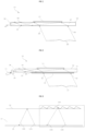
FIG 1 illustrates anoptical system 10 according to one embodiment of the present invention. Theoptical system 10 comprises atransparent optic 12 defining anoptical volume 37 and afirst turning optic 13. Theoptical system 10 captures light from ascene 15 or sources in front of it. Light from thescene 15 enters theoptical volume 37. Upon entering theoptical volume 37, light reaches thefirst turning optic 13 and gets turned in a manner to be contained within theoptical volume 37. Upon traveling a certain distance inside theoptical volume 37, the light reaches aside face 36 and exits theoptical volume 37. The term optical volume herein refers to the volume wherein the light undergoes to and forth reflection before exiting thetransparent optic 12. The side face 36 may be at an angle to the firstmain face 35 or the secondmain face 34. The side face 36 may be perpendicular to either the firstmain face 35 or the secondmain face 34. Depicted inFIG 1 are two light rays emerging from different portion of thescene 15 wherein on entering the optical volume, reach theside face 36 at different angles of incidence. -
FIG 2 discloses anoptical system 10 in combination with aphotosensor assembly 11 according to an embodiment herein. In the shown example ofFIG 2 , the light from a light source orscene 15 reaches thesecondary turning optic 14. Thesecondary turning optic 14 directs the light at a prescribed angle onto the firstmain face 35. For example, the prescribed angle is glancing. In the show example ofFIG 2 , thesecondary turning optic 14 is coupled to the firstmain face 35 via alayer 48 having a refractive index lower than the refractive index of theoptical volume 37. The firstmain face 35 is adapted to admit the light. The light admitted by the firstmain face 35 enters theoptical volume 37. The admitted light inside the optical volume reaches thefirst turning optic 13. Thefirst turning optic 13 is arranged on at least a portion of the secondmain face 34. Thefirst turning optic 13 turns the light such that the light travels in a confined manner between the secondmain face 34 and the firstmain face 35 to reach theside face 36. The light exits theoptical volume 37 through theside face 36 and is altered by atertiary optic 38 such as a lens or a grating to reach thephotosensor assembly 11. Thephotosensor assembly 11 is capable of detecting the light collected from different parts of thescene 15. This is due to a piece-wise spatial relationship preserving aspect of theoptical system 10. The spatial relationships of light from within atleast a subset of the scene are preserved when the light reaches thephotosensor assembly 11. While the spatial relationships of the whole scene may be preserved in some embodiments, it is sufficient in other embodiments that they are preserved within a subset of the scene while not necessarily the whole scene. Theoptical system 10 is also capable of preserving angular relationships in a piece wise manner. - This provides the advantage of the
optical system 10 collecting light from alarge area scene 15 or source and condensing it to asmaller photosensor assembly 11. Also provides reduction in the distance between thescene 15 and theoptical system 10. Conventional system, such as a lens does not provide the advantage of reduction in the distance. Also, the lens has the disadvantage of being bulky. Theoptical system 10 described in the embodiments herein provides a compact and substantially flat configuration. - Referring still to
FIG 2 , the propagation of light from the scene to thephotosensor assembly 11 is illustrated by therays rays first turning optic 13 undergo a change in the angle when they are reflected back into theoptical volume 37. Therays main face 35, wherein therays optical volume 37. This process repeats until therays first turning optic 13. Theray 39 proximate to theside face 36 undergoes a smaller number of reflections in theoptical volume 37 than thedistal ray 40. Hence theray 40 experiences a higher change in angle than theray 39. In his manner, the spatial relationships are converted into angular relationships and preserved. Upon reaching beyond thefirst turning optic 13, therays side face 36, via which they exit theoptical volume 37. Thus, therays optical volume 37, wherein the reflections caused by thefirst turning optic 13 causes change in angle and the reflections beyond the portion of thefirst turning optic 13 does not cause change in angle. Thetertiary optic 38 transfers the angular spread of therays photosensor assembly 11 such that different pixels of thephotosensor assembly 11 are illuminated from therays light rays scene 15 are preserved at thephotosensor assembly 11. -
FIG 3 illustrates atransparent optic 12 and a first turning optic in more detail according to an embodiment herein. According to an embodiment, thefirst turning optic 13 comprises an array ofgeometrical structures 105 for turning the light. In the shown example ofFIG 3 , an array of prisms is illustrated as thegeometrical structure 105. The light rays 106 entering the firstmain face 35 and reaching thefirst turning optic 13 continue into thegeometrical structures 105 and are reflected as the light rays 104 with an added turn angle. However, upon exiting thefirst turning optic 13, the reflection of light is determined by the geometry of the secondmain face 34 and the firstmain face 35 and may not experience the added turning angle imparted by thefirst turning optic 13, as illustrated by the light rays 103 and 102. According to one embodiment, thefirst turning optic 13 may be clamped or glued to an existingtransparent optic 12 such as a glass window. According to another embodiment herein, thefirst turning optic 13 may be embossed, inscribed or machined into thetransparent optic 12. Thetransparent optic 12 can be implemented using an off the shelf glass, acrylic or any other transparent slab wherein the first main face and the secondmain face 34 may be parallel to each other. This reduces the cost of the optical system and eases transportation and installation. However, the transparent optic can also be implemented using devices wherein the first main face and the second main face are not parallel, i.e., are at an angle. -
FIG 4 illustrates an array of geometrical structures of a first turning optic according to another embodiment herein. In the shown example ofFIG 4 , an array of trapezoidal structures is illustrated as thegeometrical structures 105. The light rays 140 and 143 are reflected by the trapezoidal structures with the added turning angle. According to another embodiment, thefirst turning optic 13 can also comprise varying refractive index materials, laterally varying geometries, laterally varying graded refractive index materials. According to yet another embodiment, the first turning optic can also comprise of layers of thin films of varying refractive indices, each of which could further comprise of laterally varying refractive index. - Referring now to
FIG 5 , according to one embodiment, a further compact form of theoptical system 10 is achieved using an additionaltransparent optic 20 and acoupler 19. The additionaltransparent optic 20 defines an additional optical volume 37b. The optical volume 37a and the additional optical volume 37b defined by thetransparent optic 12 and the additionaltransparent optic 20 together define theoptical volume 37.. As described inFIG 5 , thetransparent optic 12 comprises thefirst turning optic 13. Light rays 39 from thescene 15 enter into the optical volume 37a and propagate towards thecoupler 19. Thecoupler 19 will re-direct the light from thetransparent optic 12 to the additionaltransparent optic 20. The additionaltransparent optic 20 may redirect the light towards the optic 38. The embodiment provides the advantage of compacting the overall form factor towards smaller area footprint when the trade-off is favorable. For example, in fields of proximate imaging in the context of machine vision and industrial automation, the size of the optical system may be restricted by the space available. -
FIG 6 illustrates an exemplary coupler according to one embodiment herein. In the shown example ofFIG 6 , thecoupler 19 comprises a pair of prism 21a and 21b that reverse the light after shifting in one direction. - Referring now to
FIG 7 , according to one embodiment, aportion 12a of thetransparent optic 12 comprises a geometry of a wedge. The wedge geometry of theportion 12a is used for turning the light rays 39 in conjunction with thefirst turning optic 13. Since thefirst turning optic 13 is dedicated to turning the light rays 39 and reduce angle between the critical angle for exit, a higher flexibility is possible in the case of wedge designs. According to an embodiment, the wedge geometry of theportion 12a may taper in the opposite direction, as illustrated inFIG 8 . - Referring now to
FIG 9 , according to one embodiment, thetransparent optic 12 may comprise a curved geometrical structure. As illustrated inFIG 9 , the light rays 39, 40 from thescene 15 reach the curved geometrical structure of theoptical volume 37 and meet thefirst turning optic 13. As depicted inFIG 9 , thefirst turning optic 13 directs the light rays 39, 40 towards theside face 36 towards acoupling optic 38. The rays after exiting theoptical volume 37 are conditioned to reach thephotosensor assembly 11. In one embodiment, thefirst turning optic 13 is placed on the convex face of theoptical volume 37 in order to accept light from the concave side. An opposite configuration is achievable by changing the location of thefirst turning optic 13 from the convex to the concave face. In this case, imaging can be performed on the convex surface. Such an optical system, where the transparent optical volume has a curved geometrical structure can be used to scan curved objects like bottle labels, hand biometrics on door handles etc. - Referring now to
FIG 10 , according to one embodiment, a plurality of image sensors may be used for capturing light from different viewpoints. As depicted in the example ofFIG 10 , theoptical system 10, comprises thephotosensor assembly 11 and anadditional photosensor assembly 101 for capturing light from different viewpoints of thescene 15. Different light rays, depicted as 39 and 40, from a particular point, reach thefirst turning optic 13 at different positions. Thetertiary optics photosensor assembly 11 and theadditional photosensor assembly 101 respectively for capturing the light rays 39, 40 from different viewpoints. Using two imaging sensors, i.e., thephotosensor assembly 11 and theadditional photosensor assembly 101 allow for 3D image capturing via stereo. Use of three or more image sensors may provide the advantage of capturing the light field. Such a device could also function as a goniometer. -
FIG 11 illustrates an exemplary example of afirst turning optic 13 according to an embodiment herein. As illustrated in the shown example ofFIG 11 , a plurality of prismatic or trapezoid structures arranged adjacent to each other but curved in a lateral direction are illustrated as thegeometrical structures 105 of thefirst turning optic 13. As illustrated in the example ofFIG 11 , the curvature provides the advantage of capturing multiple views of the scene and the parameters such as aspect ratio, distortion, and the like. with increased accuracy. In the example ofFIG 11 , the curvedgeometrical structures 105 turn the incidentlight ray 39 such that the light rays 39 are turned into a plurality of different planes. - According to another embodiment, as depicted in
FIG 12 , a plurality of prismatic or trapezoid structures arranged adjacent to each other but curved in the lateral direction are illustrated as thegeometrical structures 105 of thefirst turning optic 13. According to one embodiment, thefirst turning optic 13 comprises one or moresecondary turns 116. This provides the advantage of imaging targets from different directions surrounding the target. The data can then be read out to form a 3D surface image or panoramic image. -
FIG 13 illustrates an exemplary side view of atransparent optic 12, wherein theoptical volume 37 defines a plurality of zones formed due to thefirst turning optic 13 ofFIG 11 andFIG 12 . As depicted, theoptical volume 37 defines twozones 123 and 124 whereinrays 39 reach the target at a certain angle whereas rays 39' reach the target at different angles. This provides the benefit of imaging targets from different directions surrounding the target. The data can then be read out to form a 3D surface image or panoramic image. -
FIG 14 illustrates a transparent optic according to an embodiment herein. As depicted in the example ofFIG 14 , anoptical volume 37 defined by thetransparent optic 12 is hollow. Theoptical volume 37 being hollow comprises additional layers of optics. The additional layers ofoptics 104 may be arranged on any one of the internal surface of thetransparent optic 12 or on both the internal surfaces. The optic 104 may be a turning optic. -
FIG 15 illustrates an embodiment wherein a series ofoptical sheets 104 may be arranged into the hollowoptical volume 37. For example, structural members may be used to support theoptical sheets 104 in position. Such an embodiment also allows for flexibility and stretch-ability. According to an embodiment, one or more sides of the internal surfaces may be coated with an antireflection coating. - In another embodiment, as depicted in
FIG 16 , thetransparent optic 12 comprises three optical surfaces. Light enters the firstoptical surface 1002 and is redirected by theturning optic 1003 to be contained between the twosurfaces transparent optic 12. In the shown example ofFIG 16 , the light exiting thetransparent optic 12 is incident onto aphotosensor assembly 11. As seen inFIG 16 , a portion of one of the surfaces comprises a polygonal structure configured in such a manner that light reflecting between the two surfaces does not change the relative angle of reflection, whereas in anotherportion 1003, the angle is increased or decreased. Thestructures 1003 could be a quadrilateral in cross section.FIG 17 illustrates anoptical system 10 according to another embodiment herein. In the shown example ofFIG 17 , thetransparent optic 12 defines an optical volume comprising a cylindrical structure. According to one embodiment, theoptical volume 37 comprises a plurality of layers of optics on one of either of the internal surfaces. Thefirst turning optic 13 is arranged on the secondmain face 34. Thesecondary turning optic 14 is coupled to the firstmain face 35 via alayer 48 having a refractive index lower than the refractive index of theoptical volume 37.FIG 18 illustrates a cross-sectional view of the transparent optic ofFIG 17 , according to an embodiment. The example ofFIG 18 depicts thefirst turning optic 13, theoptical volume 37 and thesecondary turning optic 14 coupled to thetransparent optic 12 via thelayer 48. -
FIG 19 illustrates anoptical system 10 according to another embodiment herein. In the shown example ofFIG 19 , thefirst turning optic 13 comprises an array ofgeometrical structures 105 placed adjacent to each other running along a portion of thetransparent optic 12.FIG 19 illustrates thefirst turning optic 13 which is coupled to thetransparent optic 12 via a wavelength selective filter. In the shown example ofFIG 19 , anoptical filter 753, such as a Bragg grating, is illustrated as the wavelength selective filter.Light rays 106 incident on theoptical filter 753 behave differently depending on the wavelength of light. Bragg gratings can be inscribed such that light rays of a certain wavelength reflect off the Bragg grating at a certain angle such asrays 752 reflected as 751 while rays of other wavelengths transmit through the Bragg grating and reflect off the prismatic structures such asrays 106 reflected as 104 at a different angle. Different Bragg gratings can be placed at different locations such as 753 and 754 sensitive to different wavelengths of light. - According to another embodiment, as depicted in
FIG 20 , the light rays 39 and 40 from atarget scene 15 enter theoptical volume 37 via asecondary turning optic 14 and reaches thefirst turning optic 13 to be contained within theoptical volume 37 until it reaches a redirectingoptic 802 which reflects the light towards aphotosensor assembly 11. The redirectingoptic 802 conditions the light rays 39 and 40 in such a manner that they are emitted at appropriate angles towards thephotosensor assembly 11. An advantage of such an embodiment is that thephotosensor assembly 11, the redirectingoptic 802, thefirst turning optic 13 and thesecondary turning optic 14 can be applied to an existingtransparent optic 12, such as a glass window or table and render it as an optical system for collecting light. - According to another embodiment, as depicted in
FIG 21 , theoptical system 10 comprises a plurality oftransparent optics transparent optics FIG 21 , thetransparent optics transparent optic 12a and transmitted to theexit face 36 while another range of angles of the incident light 990 are transmitted by the firsttransparent optic 12a into the secondtransparent optic 12b which then turns the light into theexit face 36. Several of suchtransparent optics - Referring now to
FIG 22 , anoptical system 10 is illustrated according to another embodiment herein. In the shown example ofFIG 22 , light from atarget scene 15 is incident on asecondary turning optic 14 and redirected to afirst turning optic 13 such that it is subsequently incident on a reflectingface 1202. In certain embodiments, the reflectingface 1202 is curved laterally. The reflectingface 1202 reflects the light to aphotosensor assembly 11. - Referring now to
FIG 23 , according to an embodiment herein, apropagation area 1402 of thetransparent optic 12 is cut laterally to comprise a triangular geometrical profile. This provides the advantage of reduced material consumption and weight. The term propagation area used herein is defined as a portion of thetransparent optic 12 where the light rays propagate through internal reflection without undergoing a turn from the first turning optic. In thepropagation area 1402, the light rays propagate through internal reflection between the firstmain face 34 and the secondmain face 35. According to an embodiment, as depicted inFIG 24 , thepropagation area 1402 can be tilted out of the plane of theoptical volume 37. According to an embodiment, as depicted inFIG 25 , aportion 1404 of thetransparent optic 12 comprising thefirst turning optic 13 may comprise a geometrical structure of a wedge. According to another embodiment, thepropagation area 1402 may comprise a triangular profile, as illustrated inFIG 24 . The illumination of the target scene can be achieved using a similarly scaled optic located on theface 36 as depicted inFIG 26 . The illumination optic 1601 is placed in a manner to direct light from asource 1602 into thesurface 36. This light exits theoptical volume 37 via thefirst turning optic 13 onto the target. This illumination pattern is optimized such that the resultant illumination from a uniformly reflecting target is uniform at thephotosensor assembly 11. - According to an embodiment, the illumination exiting out of the
transparent optic 12 is a batwing profile. - The embodiments described herein provides the advantage of the optical system collecting light from a large area of the scene or source and condensing it to a smaller photosensor assembly. Also, reduction in the distance between the scene and the optical system is achieved. Conventional system, such as a lens does not provide the advantage of reduction in the distance. Also, the conventional systems have the disadvantage of being bulky. The optical system described in the embodiments herein provides a compact and substantially flat configuration. Moreover, the optical system may be developed using a flat transparent optic, wherein the two main faces of the transparent optic are parallel. The first turning optic can be arranged on one of the main faces of the transparent optic. This provides the advantage of easy manufacturing of the optical system.
- The optical system described in the embodiments herein can be used in a 2D camera and for measuring light distribution. For example, the photosensor assembly can be an image sensor or an array of photodiodes, the secondary optic transfers the incoming light from an angular distribution to a spatial distribution on to individual pixels. The pixels are then readout to obtain the image of the scene. For example, such a system could be used in X-ray imaging, diagnostics and point of care, dental imaging, biometric imaging, imaging a meter or gauge, document scanner, borescopic imaging, and luminaires. For example, for X-ray imaging, as CMOS sensor resolutions increase, it is desirable to use a fluoroscopic chain consisting of a scintillator that fluoresces followed by a camera to image the fluorescence. Using conventional cameras creates a bulky design. The optical system described in the embodiments herein allows for a compact fluoroscopic chain. In aspects of diagnostics and point of care systems, semi-automated or fully automated systems capture light from material samples. Several samples are placed in front of the optical device. Each sample either reflects or emits light at certain wavelengths. A plurality of Photosensor assemblies can be used, each with an optical filter separating desired wavelengths. Each photosensor assembly can identify the light from a particular sample. Combining the measurements of the plurality of photosensor assemblies, each sample spectrum can be analyzed and later used to identify pathology or condition. Such a design increases through-put as well as decreases mechanical complexity of the device.
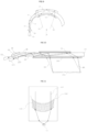
- In aspects of dental imaging, in a dental application, as depicted in
FIG 27 , instead of transferring light to a sensor, the light could be delivered to another possiblylarge area 43 to accommodate another optical device or even the eye. As, illustrated inFIG 28 , anoptical coupler 44 could be used to rotate one end of the device in order to rotate the field of view or in this case, obtain different views of upper and lower teeth. Here, the area of delivery would consist of athird turning optic 42 ofFIG 27 and afourth turning optic 41 ofFIG 27 . - In aspects of a biometric reader, the optical system can be used to read and verify a hand geometry, fingerprint, face and iris image. The concept could be used to construct a single device performing one or more of the aforementioned biometric image capture and verification. A key pad can be printed or projected on one of the faces of the optical device and using the concept of frustrated total internal reflection, the location of a key press can be detected. Thus, user interaction can be captured in this manner.
- In aspects of imaging a meter or gauge, as depicted in
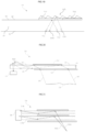
FIG 29 , theoptical system 10 is placed in front of thegage 301 to be read out (in remote monitoring or continuous monitoring scenarios) via image capturing. However, placing a camera will restrict the viewing of the gauge by a human. This may be avoided by using a transparent optic that redirects some of the light towards acamera 303 placed off-axis of the gage allowing for image capture as well as allowing auser 304 to view the gauge. - In aspects of a document Scanner,
FIG 30 illustrates a flatbed scanner device comprising the optical system described by the embodiments herein. The flatbed scanner device comprises alight source 331 that illuminates anobject 332. For example, theobject 332 may be a sheet of paper. The reflected light enters theoptical volume 37 and gets turned by thefirst turning optic 13 to reach thephotosensor assembly 11 as explained in earlier embodiments. Motion stages 333 allow for movement of thephotosensor assembly 11 enabling increase in field of view or obtain several images and reconstruct a high resolution image. The motion stage could be a motor or piezoelectric device. A configuration such as this allow for higher speed of scanning and increased throughput for automated scanning devices. - In aspects of borescopic imaging, the optical system can be used for borescopic imaging allowing for quicker image capture and simpler motion staging than existing borescopic systems.
- In aspects of luminaires, since the transparent optic can be made using thin and flexible material, it can be applied to a large surface as a ubiquitous camera. For example, a thin optic that runs all along the ceiling of a room could provide image data that could be used for occupancy sensing.
- The optical system can also be used in a 3D camera. Two or more image sensors can be placed adjacent to the photosensor assembly in order to obtain images from multiple views. The views are combined as stereo component images and a 3D image is obtained of the scene. Another embodiment is a photosensor capable of capturing spatial distribution as well as time of flight information. The sensor can obtain the time of arrival of light rays, which then coupled to the optical system allows for obtaining time of flight information of light from each point in the scene. This time of flight information could be used to create a depth map. Another embodiment is the collection of structured light reflected off a surface, which can also be used to capture 3D structure of the target.
- Additionally, the optical system can be used for light field imaging. Different groups of pixels could be used to reconstruct the light field data of the target. The optical system may also be used in a spectrometer. Apart from a lens, a grating could be placed in between the photosensor assembly and the optical volume wherein spectral data could be deciphered from the measurements. As depicted in
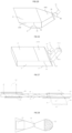
FIG 31 , theoptical system 10 is appended withseveral Bragg gratings optical system 10 and are seen to be reflected at different locations depending on the wavelength. In this manner, light sources can be combined. Theoptical system 10 may also be used as a light concentration device. Theoptical system 10 may be used to concentrate light onto photovoltaic cells and collect energy. As depicted inFIG 32 , theoptical system 10 is appended to a light collecting system such as a solar panel to increase the effective area of light collection. The optical systems 10a and 10b are placed near thesolar panel 970. Light from the sun directly reaches thesolar panel 970 as shown asrays 975 whereas therays FIG 33 , the optical system 10a and 10b can also be configured such that rays from the sun reaching the optical system 10a of thesolar collection system 976 pass through the optical system 10b and reach the solar panel of anotherdevice 977 in order to maximize power production. This is accomplished by varying the turning film parameters mechanically. - According to an embodiment, the optical system may also be used in wearable gadgets, for example a wearable glass. As the configuration of the optical system is flexible, it may be used in wearable gadgets for human. An additional function is that the device could view the iris or retina and capture images for authentication. The optical system may also be used as a user authentication card for authentication purpose. As depicted in
FIG 34 , theoptical system 10 is configured as a slim identification card such that a reader could direct light into the primary optic for illuminating a region where a finger print can be placed. The light from the finger is reflected and travels back to thereader 1110 wherein the finger print image is read. User authentication proceeds via an additional read of a magnetic or an RF card. A card swipe action whilst placing the finger on the reader would allow a simultaneous dual authentication in one swift action. - One embodiment of the geometric structure is depicted as 601 in
FIG 35 . The structure is a prism bounded by thebase face 604, the leadingedge face 602 and the trailingedge face 603. Alternatively, theface 604 could be a portion of the secondmain face 34. Aray 605 arising from thetransparent optic volume 37 passes through theface 604 and is reflected by theface 602 to return as theray 606. The reflection by theface 602 imparts a turn in the rays. In essence, if the ray were to reflect off faces 34 or 35, such a turn would not be imparted. - Still referring to
FIG 35 , the angle ofincidence 611 of theray 605 and the angle ofreflection 612 are the same as measured from the surface normal 610. However, when measured from the surface normal 615 of theface 34, theangle 614 is different from theangle 613 subtended by the reflectedray 606 at the surface normal 609. This change in angle is facilitated by the geometric structure to condition theray 605 to exit theoptical volume 37 in a prescribed manner. - The
angle 608 of the leading edge face is small in-order to impart a small turn in direction of theray 605. In a certain embodiment, theangle 608 is less than 10 degrees. In another embodiment, the angle is less than 3 degrees. In yet another embodiment, the angle is less than 1 degree. - In the embodiment where the
angle 608 is comparatively lesser, theray 605 would require a larger number of reflections to be conditioned to exit theoptical volume 37. In effect, the distance between thefaces - The second angle of the
prism 607 is less than a prescribed value. This avoids the collision ofrays 606 and theface 603, thereby preventing loss of rays or spatial structure. Since the rays may undergo multiple interactions between the prismatic structures wherein each interaction results in an additional turn, thesecond angle 607 is chosen to prevent collision of the reflected ray and theprismatic face 603 at the respective prism. Critical angle is defined as the angle of incidence above which total internal reflection occurs. In an embodiment, the second angle of theprism 607 is less than the difference of 90 degrees and critical. In a further embodiment, the second angle of theprism 607 is less than the difference 90 degrees and the sum of the critical angle and product of the number of reflections undergone by theray 605 and twice theprism angle 608. -
FIG 36 illustrates the path of a ray entering from one extreme of theface 34. Once the ray enters, it undergoes one or more reflections within theoptical volume 37. In the event of multiple reflections, the angle successively is altered and the distance between the point of reflection increases. The distance between the point of entry and the first reflection is D0 , whereas the distance between the first and the second reflection is D1 and so on. These distances are given by the following formulae.


- Where r is the angle of turn imparted at each reflection and N is the total number of reflections undergone by the ray under the influence of the turning optic.
- The length of the area adapted to admit light L is the sum of the distances D0+D1+... +DN
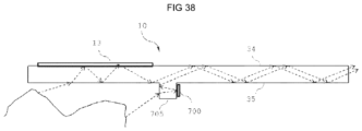
- As illustrated in
FIG 37 , the propagation area length can be reduced by imparting a further turn by 710 to the rays exiting the area adapted to receive light. Increased reflections in the propagation area allow for a decreased propagation area length. In an embodiment, the opposing faces of the propagation areas could be silvered, thus preventing the light exiting the optical volume even 5 beyond the critical angle. The opposite faces of the propagation area may be coated with bragg gratings, photonic crystals or perfect mirrors to increase the efficiency of reflection. -
FIG 38 illustrates imaging of a scene or an object from multiple angles using a monolithic piece of optic and a single light sensor, lens or camera. Light from the same or different scene coming from a different direction falls on theoffshoot area 705 and enters the optic's propagation area via aturning optic 700 which redirects light in a desired manner to reach the main optical volume. This turning optic 700 may be of the geometry of thefirst turning optic 13. Thus, light from two different directions, enters the optical volume and combines in the main optical volume to get transported to the photosensor assembly. This configuration may be used to capture side views along with the front view of objects like food items for quality control. - While this invention has been described in detail with reference to certain preferred embodiments, it should be appreciated that the present invention is not limited to those precise embodiments. Rather, in view of the present disclosure which describes the current best mode for practicing the invention, many modifications and variations would present them-selves, to those of skilled in the art without departing from the scope of this invention as defined in claims. The scope of the invention is, therefore, indicated by the following claims rather than by the foregoing description.
Claims (10)
- An optical system for collecting light from a scene (15), comprising:a single continuous transparent optic (12), a tertiary optic (38) and a photosensor assembly (11) comprising a plurality of pixels,the transparent optic (12) comprising:a first main face (35);a second main face (34) opposite to the first main face (35), wherein an optical volume (37) is defined between the first main face (35) and the second main face (34); anda first turning optic (13) arranged on the second main face (34) and configured to turn light from the scene (15) entering the transparent optic through the first main face (35) and admitted inside the optical volume (37) and passing through the second main face (34), such that the light is internally reflected within the optical volume (37), wherein the first turning optic (13) is configured to provide an added turn angle, for the admitted light passing through the second main face (34);wherein the first main face (35) is a single continuous surface throughout the transparent optic (12) and the second main face (34) is a single continuous surface throughout the transparent optic (12),wherein the first turning optic (13) includes an array of geometrical structures (105) arranged on the second main face (34) and external to the optical volume (37), such that, at each interaction with the second main face (34), the light passing through the second main face (34) enters into at least one of the array of geometrical structures (105) and is reflected by at least one face of the geometrical structure (105), such that the first turning optic (13) imparts a cumulatively larger turn angle at every interaction of the light with the first turning optic (13),wherein the tertiary optic (38) is configured to alter light that exits the optical volume (37) through the side face (36) to reach the photosensor assembly (11);wherein the optical system (10) is configured to preserve angular relationships of incident light in a piece wise manner such that the spatial relationships of light from within at least a subset of the scene (15) are preserved when the light reaches the photosensor assembly (11).
- The optical system as claimed in claim 1, wherein the first turning optic (13) is arranged on a portion of the second main face (34).
- The optical system as claimed in claim 1, wherein the geometrical structures selectively alter the direction of reflection.
- The optical system as claimed in any of the preceding claims, wherein the first turning optic (13) simultaneously direct portions of the incident light in more than one direction.
- The optical system as claimed in any of the preceding claims, wherein the first turning optic (13) is curved in one or more directions.
- The optical system as claimed in any of the preceding claims, wherein the first turning optic (13) is a layer formed on a portion of the second main face (34).
- The optical system as claimed in any of the preceding claims, wherein a wavelength selective filter is placed between the first turning optic (13) and the optical volume (37).
- The optical system as claimed in claim 1, wherein a first portion of the incident light is admitted inside the optical volume and a second portion of the incident light is transmitted.
- The optical system as claimed in claim 1, wherein the geometrical structures reflect a first portion of the incident light and transmit a second portion of the incident light.
- The optical system as claimed in claim 1, wherein each of the array of geometrical structures includes:a base face (604), a leading-edge face (602) and a trailing edge face (603);a first angle (608) of each of the array of geometrical structures is defined as an angle between the leading-edge face (602) and the base face (604); anda second angle (607) of each of the array of geometrical structures is defined as an angle between the trailing edge face (603) and the base face (604);wherein, the value of the first angle (608) is less than half the value of a critical angle, and the value of second angle (607) is less than (90-critical angle),wherein the critical angle is defined as an angle of incidence above which total internal reflection occurs.
Applications Claiming Priority (3)
| Application Number | Priority Date | Filing Date | Title |
|---|---|---|---|
| IN3352CH2013 | 2013-09-01 | ||
| IN3355CH2013 | 2013-09-01 | ||
| PCT/IB2014/064174 WO2015028991A1 (en) | 2013-09-01 | 2014-09-01 | Optical device for light collection |
Publications (2)
| Publication Number | Publication Date |
|---|---|
| EP3039473A1 EP3039473A1 (en) | 2016-07-06 |
| EP3039473B1 true EP3039473B1 (en) | 2024-04-17 |
Family
ID=51662163
Family Applications (1)
| Application Number | Title | Priority Date | Filing Date |
|---|---|---|---|
| EP14781279.6A Active EP3039473B1 (en) | 2013-09-01 | 2014-09-01 | Optical device for light collection |
Country Status (5)
| Country | Link |
|---|---|
| US (1) | US10606051B2 (en) |
| EP (1) | EP3039473B1 (en) |
| JP (2) | JP2016537683A (en) |
| CN (1) | CN105492955A (en) |
| WO (2) | WO2015028991A1 (en) |
Families Citing this family (6)
| Publication number | Priority date | Publication date | Assignee | Title |
|---|---|---|---|---|
| EP3314316A4 (en) * | 2015-06-29 | 2018-11-21 | Varun Akur Venkatesan | Optical system |
| WO2018042341A1 (en) * | 2016-08-31 | 2018-03-08 | Varun Akur Venkatesan | An optical system with turning optics |
| US20190057547A1 (en) * | 2017-08-16 | 2019-02-21 | II James A. Abraham | System and Method for Imaging a Mouth in Real Time During a Dental Procedure |
| EP3518023A1 (en) * | 2018-01-26 | 2019-07-31 | Momes GmbH | Visualisation device |
| CN109238979B (en) * | 2018-11-02 | 2021-05-07 | 京东方科技集团股份有限公司 | Light extraction device, detection device and method of use thereof |
| DE102019204875B3 (en) * | 2019-04-05 | 2020-06-18 | Audi Ag | Flatbed scanner |
Citations (3)
| Publication number | Priority date | Publication date | Assignee | Title |
|---|---|---|---|---|
| WO2002097324A1 (en) * | 2001-06-01 | 2002-12-05 | Lumileds Lighting U.S., Llc | Compact illumination system and display device |
| DE202009007565U1 (en) * | 2009-05-27 | 2010-10-14 | Hella Kgaa Hueck & Co. | Illuminated scoreboard |
| WO2012070533A1 (en) * | 2010-11-24 | 2012-05-31 | シャープ株式会社 | Solar cell module and photovolatic power generation device |
Family Cites Families (27)
| Publication number | Priority date | Publication date | Assignee | Title |
|---|---|---|---|---|
| US4863224A (en) * | 1981-10-06 | 1989-09-05 | Afian Viktor V | Solar concentrator and manufacturing method therefor |
| JPH01287785A (en) * | 1988-05-16 | 1989-11-20 | Fujitsu Ltd | Irregular shape detecting device |
| US6002829A (en) * | 1992-03-23 | 1999-12-14 | Minnesota Mining And Manufacturing Company | Luminaire device |
| JP2000221416A (en) * | 1999-02-03 | 2000-08-11 | Olympus Optical Co Ltd | Optical path conversion optical system |
| GB2360603A (en) * | 2000-03-20 | 2001-09-26 | Cambridge 3D Display Ltd | Planar optical waveguide and float glass process |
| GB0029340D0 (en) * | 2000-11-30 | 2001-01-17 | Cambridge 3D Display Ltd | Flat panel camera |
| JP2003308714A (en) | 2002-04-17 | 2003-10-31 | Fuji Photo Film Co Ltd | Light guide film |
| US7426328B2 (en) * | 2002-08-28 | 2008-09-16 | Phosistor Technologies, Inc. | Varying refractive index optical medium using at least two materials with thicknesses less than a wavelength |
| TW200413776A (en) | 2002-11-05 | 2004-08-01 | Matsushita Electric Ind Co Ltd | Display element and display using the same |
| JP2004171948A (en) * | 2002-11-20 | 2004-06-17 | Harison Toshiba Lighting Corp | Backlight model |
| US20050074204A1 (en) * | 2003-10-02 | 2005-04-07 | Gordon Wilson | Spectral plane method and apparatus for wavelength-selective optical switching |
| US7775700B2 (en) * | 2004-10-01 | 2010-08-17 | Rohm And Haas Electronics Materials Llc | Turning film using array of roof prism structures |
| JP4743846B2 (en) | 2005-05-10 | 2011-08-10 | シチズン電子株式会社 | Optical communication apparatus and information equipment using the same |
| JP2006350452A (en) * | 2005-06-13 | 2006-12-28 | Olympus Corp | Photographing display device and calibration data calculation method therefor |
| JP2006065360A (en) * | 2005-11-16 | 2006-03-09 | Omron Corp | Light guide and display apparatus |
| US7613898B2 (en) * | 2006-01-17 | 2009-11-03 | Globalfoundries Inc. | Virtualizing an IOMMU |
| JP4639337B2 (en) * | 2006-02-17 | 2011-02-23 | 国立大学法人長岡技術科学大学 | Solar cell and solar collector |
| GB0619226D0 (en) * | 2006-09-29 | 2006-11-08 | Cambridge Flat Projection | Efficient wedge projection |
| ES2642209T3 (en) * | 2007-05-01 | 2017-11-15 | Morgan Solar Inc. | Solar light guide panel and its manufacturing method |
| US20090126792A1 (en) * | 2007-11-16 | 2009-05-21 | Qualcomm Incorporated | Thin film solar concentrator/collector |
| EP2248189A1 (en) * | 2008-02-12 | 2010-11-10 | QUALCOMM MEMS Technologies, Inc. | Dual layer thin film holographic solar concentrator/ collector |
| JP2012503221A (en) * | 2008-09-18 | 2012-02-02 | クォルコム・メムズ・テクノロジーズ・インコーポレーテッド | Increasing the angular range of light collection in solar collectors / collectors |
| US7949214B2 (en) * | 2008-11-06 | 2011-05-24 | Microvision, Inc. | Substrate guided relay with pupil expanding input coupler |
| CN103335931A (en) * | 2009-07-07 | 2013-10-02 | 索尼公司 | Microfluidic device |
| WO2012147646A1 (en) * | 2011-04-28 | 2012-11-01 | シャープ株式会社 | Light source device, surface light source device, display device, and illumination device |
| JP2015035252A (en) * | 2011-11-30 | 2015-02-19 | シャープ株式会社 | Light source device, surface light source device, display device, and lighting device |
| US8979394B2 (en) * | 2013-03-28 | 2015-03-17 | Corning Cable Systems Llc | Self-contained total internal reflection sub-assembly |
-
2014
- 2014-09-01 JP JP2016537423A patent/JP2016537683A/en active Pending
- 2014-09-01 EP EP14781279.6A patent/EP3039473B1/en active Active
- 2014-09-01 WO PCT/IB2014/064174 patent/WO2015028991A1/en active Application Filing
- 2014-09-01 US US14/914,879 patent/US10606051B2/en active Active
- 2014-09-01 WO PCT/IB2014/064165 patent/WO2015028988A1/en active Application Filing
- 2014-09-01 CN CN201480048307.7A patent/CN105492955A/en active Pending
-
2018
- 2018-06-20 JP JP2018116565A patent/JP6706287B2/en active Active
Patent Citations (4)
| Publication number | Priority date | Publication date | Assignee | Title |
|---|---|---|---|---|
| WO2002097324A1 (en) * | 2001-06-01 | 2002-12-05 | Lumileds Lighting U.S., Llc | Compact illumination system and display device |
| DE202009007565U1 (en) * | 2009-05-27 | 2010-10-14 | Hella Kgaa Hueck & Co. | Illuminated scoreboard |
| WO2012070533A1 (en) * | 2010-11-24 | 2012-05-31 | シャープ株式会社 | Solar cell module and photovolatic power generation device |
| US20130240037A1 (en) * | 2010-11-24 | 2013-09-19 | Sharp Kabushiki Kaisha | Solar cell module and solar generator |
Also Published As
| Publication number | Publication date |
|---|---|
| JP2018200468A (en) | 2018-12-20 |
| JP6706287B2 (en) | 2020-06-03 |
| WO2015028991A4 (en) | 2015-05-07 |
| JP2016537683A (en) | 2016-12-01 |
| US10606051B2 (en) | 2020-03-31 |
| US20160209633A1 (en) | 2016-07-21 |
| EP3039473A1 (en) | 2016-07-06 |
| CN105492955A (en) | 2016-04-13 |
| WO2015028991A1 (en) | 2015-03-05 |
| WO2015028988A1 (en) | 2015-03-05 |
Similar Documents
| Publication | Publication Date | Title |
|---|---|---|
| EP3039473B1 (en) | Optical device for light collection | |
| KR101981730B1 (en) | Ambient light illumination for non-imaging contact sensors | |
| US10366273B2 (en) | Device for the contact-based simultaneous capture of prints of autopodia | |
| RU2532696C2 (en) | Lighting device for touch- and object-sensitive display | |
| KR102298500B1 (en) | Head-mounted display with an eyeball-tracker integrated system | |
| CN107407598A (en) | Glass waveguide spectrophotometer | |
| CN114143435A (en) | Method and system for multiple F-value shots | |
| US20150281535A1 (en) | Imaging device and analyzing apparatus using the imaging device | |
| WO2015137880A1 (en) | An optical interference device | |
| US8952317B2 (en) | Apparatus for the analysis of an object, preferably of a document of value, using optical radiation | |
| CN102564980A (en) | Optical device and electronic apparatus | |
| JP5820845B2 (en) | Illumination device, image sensor unit, and paper sheet identification device | |
| RU2528036C2 (en) | Optical system and sensor for inspecting valuable documents having said optical system | |
| RU2484524C1 (en) | System for recording papillary patterns | |
| CN111723621B (en) | Image acquisition device and electronic equipment | |
| US6409088B1 (en) | Scanning device for capturing images | |
| WO2017002008A1 (en) | Optical system | |
| TWI822342B (en) | Hyperspectral camera | |
| KR20230164376A (en) | Optical apparatus | |
| RU2172982C1 (en) | Securities image reader | |
| CN107402439B (en) | Thin plate imaging device | |
| JP4390334B2 (en) | Pattern detector | |
| JP2023136779A (en) | Coin image sensor, coin identification device, coin processing apparatus, and coin image capturing method | |
| CN202837179U (en) | Spherical reflectivity measuring device | |
| WO2015028993A1 (en) | Hand geometry reader |
Legal Events
| Date | Code | Title | Description |
|---|---|---|---|
| PUAI | Public reference made under article 153(3) epc to a published international application that has entered the european phase |
Free format text: ORIGINAL CODE: 0009012 |
|
| 17P | Request for examination filed |
Effective date: 20160223 |
|
| AK | Designated contracting states |
Kind code of ref document: A1 Designated state(s): AL AT BE BG CH CY CZ DE DK EE ES FI FR GB GR HR HU IE IS IT LI LT LU LV MC MK MT NL NO PL PT RO RS SE SI SK SM TR |
|
| AX | Request for extension of the european patent |
Extension state: BA ME |
|
| DAX | Request for extension of the european patent (deleted) | ||
| STAA | Information on the status of an ep patent application or granted ep patent |
Free format text: STATUS: EXAMINATION IS IN PROGRESS |
|
| 17Q | First examination report despatched |
Effective date: 20191002 |
|
| STAA | Information on the status of an ep patent application or granted ep patent |
Free format text: STATUS: EXAMINATION IS IN PROGRESS |
|
| STAA | Information on the status of an ep patent application or granted ep patent |
Free format text: STATUS: EXAMINATION IS IN PROGRESS |
|
| GRAP | Despatch of communication of intention to grant a patent |
Free format text: ORIGINAL CODE: EPIDOSNIGR1 |
|
| STAA | Information on the status of an ep patent application or granted ep patent |
Free format text: STATUS: GRANT OF PATENT IS INTENDED |
|
| INTG | Intention to grant announced |
Effective date: 20231211 |
|
| GRAS | Grant fee paid |
Free format text: ORIGINAL CODE: EPIDOSNIGR3 |
|
| GRAA | (expected) grant |
Free format text: ORIGINAL CODE: 0009210 |
|
| STAA | Information on the status of an ep patent application or granted ep patent |
Free format text: STATUS: THE PATENT HAS BEEN GRANTED |
|
| AK | Designated contracting states |
Kind code of ref document: B1 Designated state(s): AL AT BE BG CH CY CZ DE DK EE ES FI FR GB GR HR HU IE IS IT LI LT LU LV MC MK MT NL NO PL PT RO RS SE SI SK SM TR |
|
| REG | Reference to a national code |
Ref country code: GB Ref legal event code: FG4D |