EP3038436B1 - Production of a circuit assembly with thermal vias - Google Patents
Production of a circuit assembly with thermal vias Download PDFInfo
- Publication number
- EP3038436B1 EP3038436B1 EP15197167.8A EP15197167A EP3038436B1 EP 3038436 B1 EP3038436 B1 EP 3038436B1 EP 15197167 A EP15197167 A EP 15197167A EP 3038436 B1 EP3038436 B1 EP 3038436B1
- Authority
- EP
- European Patent Office
- Prior art keywords
- vias
- circuit board
- thermal
- thermal vias
- solder
- Prior art date
- Legal status (The legal status is an assumption and is not a legal conclusion. Google has not performed a legal analysis and makes no representation as to the accuracy of the status listed.)
- Active
Links
- 238000004519 manufacturing process Methods 0.000 title description 4
- 229910000679 solder Inorganic materials 0.000 claims description 30
- 238000000034 method Methods 0.000 claims description 25
- 239000000463 material Substances 0.000 claims description 13
- 238000005476 soldering Methods 0.000 claims description 13
- 239000012777 electrically insulating material Substances 0.000 claims description 4
- 239000010410 layer Substances 0.000 description 19
- 230000017525 heat dissipation Effects 0.000 description 6
- 238000001816 cooling Methods 0.000 description 5
- 238000010292 electrical insulation Methods 0.000 description 4
- 238000013459 approach Methods 0.000 description 3
- 239000004020 conductor Substances 0.000 description 3
- BQCADISMDOOEFD-UHFFFAOYSA-N Silver Chemical compound [Ag] BQCADISMDOOEFD-UHFFFAOYSA-N 0.000 description 2
- 239000012790 adhesive layer Substances 0.000 description 2
- 239000003570 air Substances 0.000 description 2
- 230000015572 biosynthetic process Effects 0.000 description 2
- 229910052802 copper Inorganic materials 0.000 description 2
- 239000010949 copper Substances 0.000 description 2
- 230000002349 favourable effect Effects 0.000 description 2
- 238000007639 printing Methods 0.000 description 2
- 229910052709 silver Inorganic materials 0.000 description 2
- 239000004332 silver Substances 0.000 description 2
- 241001463014 Chazara briseis Species 0.000 description 1
- RYGMFSIKBFXOCR-UHFFFAOYSA-N Copper Chemical compound [Cu] RYGMFSIKBFXOCR-UHFFFAOYSA-N 0.000 description 1
- 239000012080 ambient air Substances 0.000 description 1
- 230000004888 barrier function Effects 0.000 description 1
- 239000002131 composite material Substances 0.000 description 1
- 239000002826 coolant Substances 0.000 description 1
- 238000013461 design Methods 0.000 description 1
- 238000011161 development Methods 0.000 description 1
- 239000011152 fibreglass Substances 0.000 description 1
- 230000001771 impaired effect Effects 0.000 description 1
- 238000009413 insulation Methods 0.000 description 1
- 230000010354 integration Effects 0.000 description 1
- 238000002955 isolation Methods 0.000 description 1
- 239000007769 metal material Substances 0.000 description 1
- 238000012856 packing Methods 0.000 description 1
- 239000004033 plastic Substances 0.000 description 1
- 238000007650 screen-printing Methods 0.000 description 1
- 238000012546 transfer Methods 0.000 description 1
Images


Classifications
-
- H—ELECTRICITY
- H05—ELECTRIC TECHNIQUES NOT OTHERWISE PROVIDED FOR
- H05K—PRINTED CIRCUITS; CASINGS OR CONSTRUCTIONAL DETAILS OF ELECTRIC APPARATUS; MANUFACTURE OF ASSEMBLAGES OF ELECTRICAL COMPONENTS
- H05K1/00—Printed circuits
- H05K1/02—Details
- H05K1/0201—Thermal arrangements, e.g. for cooling, heating or preventing overheating
- H05K1/0203—Cooling of mounted components
- H05K1/0204—Cooling of mounted components using means for thermal conduction connection in the thickness direction of the substrate
- H05K1/0206—Cooling of mounted components using means for thermal conduction connection in the thickness direction of the substrate by printed thermal vias
-
- H—ELECTRICITY
- H05—ELECTRIC TECHNIQUES NOT OTHERWISE PROVIDED FOR
- H05K—PRINTED CIRCUITS; CASINGS OR CONSTRUCTIONAL DETAILS OF ELECTRIC APPARATUS; MANUFACTURE OF ASSEMBLAGES OF ELECTRICAL COMPONENTS
- H05K3/00—Apparatus or processes for manufacturing printed circuits
- H05K3/0094—Filling or covering plated through-holes or blind plated vias, e.g. for masking or for mechanical reinforcement
-
- H—ELECTRICITY
- H05—ELECTRIC TECHNIQUES NOT OTHERWISE PROVIDED FOR
- H05K—PRINTED CIRCUITS; CASINGS OR CONSTRUCTIONAL DETAILS OF ELECTRIC APPARATUS; MANUFACTURE OF ASSEMBLAGES OF ELECTRICAL COMPONENTS
- H05K3/00—Apparatus or processes for manufacturing printed circuits
- H05K3/30—Assembling printed circuits with electric components, e.g. with resistor
- H05K3/32—Assembling printed circuits with electric components, e.g. with resistor electrically connecting electric components or wires to printed circuits
- H05K3/34—Assembling printed circuits with electric components, e.g. with resistor electrically connecting electric components or wires to printed circuits by soldering
- H05K3/341—Surface mounted components
-
- H—ELECTRICITY
- H05—ELECTRIC TECHNIQUES NOT OTHERWISE PROVIDED FOR
- H05K—PRINTED CIRCUITS; CASINGS OR CONSTRUCTIONAL DETAILS OF ELECTRIC APPARATUS; MANUFACTURE OF ASSEMBLAGES OF ELECTRICAL COMPONENTS
- H05K7/00—Constructional details common to different types of electric apparatus
- H05K7/20—Modifications to facilitate cooling, ventilating, or heating
- H05K7/2039—Modifications to facilitate cooling, ventilating, or heating characterised by the heat transfer by conduction from the heat generating element to a dissipating body
- H05K7/205—Heat-dissipating body thermally connected to heat generating element via thermal paths through printed circuit board [PCB]
-
- H—ELECTRICITY
- H05—ELECTRIC TECHNIQUES NOT OTHERWISE PROVIDED FOR
- H05K—PRINTED CIRCUITS; CASINGS OR CONSTRUCTIONAL DETAILS OF ELECTRIC APPARATUS; MANUFACTURE OF ASSEMBLAGES OF ELECTRICAL COMPONENTS
- H05K7/00—Constructional details common to different types of electric apparatus
- H05K7/20—Modifications to facilitate cooling, ventilating, or heating
- H05K7/20845—Modifications to facilitate cooling, ventilating, or heating for automotive electronic casings
- H05K7/20854—Heat transfer by conduction from internal heat source to heat radiating structure
-
- H—ELECTRICITY
- H01—ELECTRIC ELEMENTS
- H01L—SEMICONDUCTOR DEVICES NOT COVERED BY CLASS H10
- H01L23/00—Details of semiconductor or other solid state devices
- H01L23/34—Arrangements for cooling, heating, ventilating or temperature compensation ; Temperature sensing arrangements
- H01L23/36—Selection of materials, or shaping, to facilitate cooling or heating, e.g. heatsinks
- H01L23/367—Cooling facilitated by shape of device
- H01L23/3677—Wire-like or pin-like cooling fins or heat sinks
-
- H—ELECTRICITY
- H05—ELECTRIC TECHNIQUES NOT OTHERWISE PROVIDED FOR
- H05K—PRINTED CIRCUITS; CASINGS OR CONSTRUCTIONAL DETAILS OF ELECTRIC APPARATUS; MANUFACTURE OF ASSEMBLAGES OF ELECTRICAL COMPONENTS
- H05K1/00—Printed circuits
- H05K1/02—Details
- H05K1/11—Printed elements for providing electric connections to or between printed circuits
- H05K1/111—Pads for surface mounting, e.g. lay-out
- H05K1/112—Pads for surface mounting, e.g. lay-out directly combined with via connections
- H05K1/113—Via provided in pad; Pad over filled via
-
- H—ELECTRICITY
- H05—ELECTRIC TECHNIQUES NOT OTHERWISE PROVIDED FOR
- H05K—PRINTED CIRCUITS; CASINGS OR CONSTRUCTIONAL DETAILS OF ELECTRIC APPARATUS; MANUFACTURE OF ASSEMBLAGES OF ELECTRICAL COMPONENTS
- H05K2201/00—Indexing scheme relating to printed circuits covered by H05K1/00
- H05K2201/06—Thermal details
- H05K2201/066—Heatsink mounted on the surface of the PCB
-
- H—ELECTRICITY
- H05—ELECTRIC TECHNIQUES NOT OTHERWISE PROVIDED FOR
- H05K—PRINTED CIRCUITS; CASINGS OR CONSTRUCTIONAL DETAILS OF ELECTRIC APPARATUS; MANUFACTURE OF ASSEMBLAGES OF ELECTRICAL COMPONENTS
- H05K2201/00—Indexing scheme relating to printed circuits covered by H05K1/00
- H05K2201/09—Shape and layout
- H05K2201/09209—Shape and layout details of conductors
- H05K2201/095—Conductive through-holes or vias
- H05K2201/09572—Solder filled plated through-hole in the final product
-
- H—ELECTRICITY
- H05—ELECTRIC TECHNIQUES NOT OTHERWISE PROVIDED FOR
- H05K—PRINTED CIRCUITS; CASINGS OR CONSTRUCTIONAL DETAILS OF ELECTRIC APPARATUS; MANUFACTURE OF ASSEMBLAGES OF ELECTRICAL COMPONENTS
- H05K2201/00—Indexing scheme relating to printed circuits covered by H05K1/00
- H05K2201/10—Details of components or other objects attached to or integrated in a printed circuit board
- H05K2201/10007—Types of components
- H05K2201/10106—Light emitting diode [LED]
-
- H—ELECTRICITY
- H05—ELECTRIC TECHNIQUES NOT OTHERWISE PROVIDED FOR
- H05K—PRINTED CIRCUITS; CASINGS OR CONSTRUCTIONAL DETAILS OF ELECTRIC APPARATUS; MANUFACTURE OF ASSEMBLAGES OF ELECTRICAL COMPONENTS
- H05K2201/00—Indexing scheme relating to printed circuits covered by H05K1/00
- H05K2201/10—Details of components or other objects attached to or integrated in a printed circuit board
- H05K2201/10613—Details of electrical connections of non-printed components, e.g. special leads
- H05K2201/10954—Other details of electrical connections
- H05K2201/10969—Metallic case or integral heatsink of component electrically connected to a pad on PCB
-
- H—ELECTRICITY
- H05—ELECTRIC TECHNIQUES NOT OTHERWISE PROVIDED FOR
- H05K—PRINTED CIRCUITS; CASINGS OR CONSTRUCTIONAL DETAILS OF ELECTRIC APPARATUS; MANUFACTURE OF ASSEMBLAGES OF ELECTRICAL COMPONENTS
- H05K2203/00—Indexing scheme relating to apparatus or processes for manufacturing printed circuits covered by H05K3/00
- H05K2203/04—Soldering or other types of metallurgic bonding
- H05K2203/0455—PTH for surface mount device [SMD], e.g. wherein solder flows through the PTH during mounting
-
- H—ELECTRICITY
- H05—ELECTRIC TECHNIQUES NOT OTHERWISE PROVIDED FOR
- H05K—PRINTED CIRCUITS; CASINGS OR CONSTRUCTIONAL DETAILS OF ELECTRIC APPARATUS; MANUFACTURE OF ASSEMBLAGES OF ELECTRICAL COMPONENTS
- H05K3/00—Apparatus or processes for manufacturing printed circuits
- H05K3/0058—Laminating printed circuit boards onto other substrates, e.g. metallic substrates
-
- H—ELECTRICITY
- H05—ELECTRIC TECHNIQUES NOT OTHERWISE PROVIDED FOR
- H05K—PRINTED CIRCUITS; CASINGS OR CONSTRUCTIONAL DETAILS OF ELECTRIC APPARATUS; MANUFACTURE OF ASSEMBLAGES OF ELECTRICAL COMPONENTS
- H05K3/00—Apparatus or processes for manufacturing printed circuits
- H05K3/10—Apparatus or processes for manufacturing printed circuits in which conductive material is applied to the insulating support in such a manner as to form the desired conductive pattern
- H05K3/12—Apparatus or processes for manufacturing printed circuits in which conductive material is applied to the insulating support in such a manner as to form the desired conductive pattern using thick film techniques, e.g. printing techniques to apply the conductive material or similar techniques for applying conductive paste or ink patterns
- H05K3/1216—Apparatus or processes for manufacturing printed circuits in which conductive material is applied to the insulating support in such a manner as to form the desired conductive pattern using thick film techniques, e.g. printing techniques to apply the conductive material or similar techniques for applying conductive paste or ink patterns by screen printing or stencil printing
-
- H—ELECTRICITY
- H05—ELECTRIC TECHNIQUES NOT OTHERWISE PROVIDED FOR
- H05K—PRINTED CIRCUITS; CASINGS OR CONSTRUCTIONAL DETAILS OF ELECTRIC APPARATUS; MANUFACTURE OF ASSEMBLAGES OF ELECTRICAL COMPONENTS
- H05K3/00—Apparatus or processes for manufacturing printed circuits
- H05K3/30—Assembling printed circuits with electric components, e.g. with resistor
- H05K3/32—Assembling printed circuits with electric components, e.g. with resistor electrically connecting electric components or wires to printed circuits
- H05K3/34—Assembling printed circuits with electric components, e.g. with resistor electrically connecting electric components or wires to printed circuits by soldering
- H05K3/3452—Solder masks
-
- Y—GENERAL TAGGING OF NEW TECHNOLOGICAL DEVELOPMENTS; GENERAL TAGGING OF CROSS-SECTIONAL TECHNOLOGIES SPANNING OVER SEVERAL SECTIONS OF THE IPC; TECHNICAL SUBJECTS COVERED BY FORMER USPC CROSS-REFERENCE ART COLLECTIONS [XRACs] AND DIGESTS
- Y02—TECHNOLOGIES OR APPLICATIONS FOR MITIGATION OR ADAPTATION AGAINST CLIMATE CHANGE
- Y02P—CLIMATE CHANGE MITIGATION TECHNOLOGIES IN THE PRODUCTION OR PROCESSING OF GOODS
- Y02P70/00—Climate change mitigation technologies in the production process for final industrial or consumer products
- Y02P70/50—Manufacturing or production processes characterised by the final manufactured product
Definitions
- the invention relates to a method for producing a circuit arrangement on a carrier plate, in which components are applied to an upper side of the printed circuit board, the printed circuit board having thermal vias which run through the printed circuit board to an underside opposite the upper side.
- Circuit arrangements of the type considered here are typically implemented on a printed circuit board which, as a carrier plate, carries a number of electronic components ("parts"), as a rule on one of the two sides of the printed circuit board.
- This side carrying the components is referred to in the context of this disclosure in accordance with the usual terminology as the "upper side”; the side opposite this is referred to as the "underside”.
- Electrical connection lines for the electronic components can be located on both sides of the circuit board, typically predominantly on the underside.
- the circuit board is conventionally made of a plastic or composite material such as FR4, an epoxy-fiberglass material; suitable circuit board materials are known per se and are not the subject of the invention.
- heat spreading surfaces are provided, i.e. surfaces made of thermally conductive material on a surface of the circuit board, which are in thermal contact with the component to be cooled. Such a heat spreading surface leads to an effective enlargement of the thermal surface of the component, via which heat can be given off.
- the thermal budget on a circuit board is becoming more and more critical due to the increasing integration and the ever increasing packing density, which results, among other things, from limitations in the space available for the circuit board and / or its components. Of the The free space required for thermally stressed components that can be used for heat spreading surfaces is therefore increasingly no longer available in sufficient size.
- heat spreading surfaces have the further disadvantage that the heat is only dissipated to the ambient air and not into a heat sink.
- the thermal vias are mostly outside the surfaces to be soldered, thus not directly in the component pads, which makes it difficult to dissipate the heat;
- expanded pad areas are necessary, so that thermal vias that are outside the component pads, in turn, lead to increased space requirements.
- thermal vias are placed in the component pads and are already filled ("plugged") with components, for example by the manufacturer of the printed circuit board, before they are fitted.
- Such filled vias meet the technical specifications, but are expensive.
- thermal vias often cannot be arranged in the most effective place and therefore do not provide optimal heat dissipation.
- unfilled vias only have a small surface area for heat dissipation and thus result in a limited conductivity of the heat path from the component to the heat sink.
- EP 0 869 704 A1 describes a method according to the preamble of claim 1, wherein after the thermal vias have been filled, a thermal adhesive layer is formed on the underside.
- DE 199 09 505 A1 describes an application of a screen printing material on the underside of the carrier body, which penetrates into the plated-through holes.
- This solution according to the invention contains as a basic idea that a layer of thermally conductive, electrically insulating material is applied in a first process step to the back of the printed circuit board, for example by a printing process of a type known per se. TIM), such as thermal paste, can be considered.
- thermal conductivity is to be understood as meaning a material which has a comparatively high thermal conductivity, which makes it suitable for use in a thermal via.
- thermal conductivity is above that of the Carrier plate is, preferably by at least one order of magnitude or by several orders of magnitude.
- This layer leads to little or no additional costs, and nevertheless an optimal thermal dissipation of the heat from components on the upper side of the circuit board to the heat sink can be ensured.
- the method according to the invention is particularly suitable for use in the production of a printed circuit board of a vehicle headlight, the printed circuit board comprising a carrier plate with at least one thermal through-hole contact, which is located in the area of a connection pad of a light-generating component. This plated-through hole is thus filled according to the method according to the invention.
- the cooling capacity can be additionally increased on the one hand and a simple design of the TIM layer can be used on the other hand if the layer applied in step a) jointly covers the opening of several vias on the underside.
- the thermal vias in step a) can remain at least predominantly free in their areas between the bottom and the top and only be filled in step b).
- step b) can be carried out by a soldering process at elevated temperature, preferably a reflow process.
- the components can advantageously be fitted between steps a) and b), for example by first applying solder paste to the thermal vias on the top after step a) and then fitting the components.
- a circuit board 30 is shown in which two solder-filled thermal vias 34, 35 are provided in the area of a pad 38 of a component 39 which is arranged on the top 31 of the circuit board 30 and which is via the thermal vias filled with solder 33 34, 35 is to be cooled via the underside 32.
- a circuit board 30 is shown in which two solder-filled thermal vias 34, 35 are provided in the area of a pad 38 of a component 39 which is arranged on the top 31 of the circuit board 30 and which is via the thermal vias filled with solder 33 34, 35 is to be cooled via the underside 32.
- Fig. 1 illustrates the problems that can arise with thermal vias of this type. Both vias are open towards the bottom 32.
- via 34 for example, this has the result that it was incompletely filled with solder 33 and / or solder has flowed off to the bottom 32; Solder that has flowed off can, for example, have dripped off or run off to the side, where it can possibly form disruptive drops 36. Even if a via 35 remains completely filled with solder 33, it must be expected that a more or less large part of the solder will run off through the via during the soldering process, which can lead to solder in the area of the pad 38 on the upper side 31 is absent, so that voids 37 form in the solder, which reduce the thermal conductivity and thus hinder the dissipation of heat from the component 39 to the underside 32.
- a layer of a TIM is printed on the underside of the circuit board.
- the TIM has a high thermal conductivity and sufficient electrical insulation strength. This makes it possible to place thermal vias directly in the pads of thermally stressed components - such as LEDs for headlights - without this leading to the disadvantages described above. This is explained below with the embodiment of FIG Figures 2a to 2c explained.
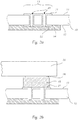
- FIG. 10 shows a circuit board 10 which is structurally similar to circuit board 30 of FIG Fig. 1 is equivalent to.
- the circuit board consists for example of FR-4 material; in the area 13 of a pad, which is provided for a component to be applied to the top side 11 of the circuit board in a later step, there are two thermal vias 20 with a diameter of typically 350 ⁇ m; However, thanks to the invention, larger diameters are also possible, larger vias also being easier to fill and offering a higher overall thermal conductivity.
- the two vias 20 are representative of any number of one, two, three or more thermal vias, the number being able to be selected depending on the application and the desired heat throughput (cooling capacity) to the underside 12.
- thermal vias 20 consist of a known type each of a - usually cylindrical - bore, the inner surface of which is lined with an electrically conductive material - e.g. copper - and a flat area 21 each at the two openings on the top and bottom , 22 passes.
- the area 21 on the upper side 11 and that 22 on the lower side 12 can be the same with regard to the surface shape or (not shown) can be of different sizes.
- a layer 14 of a TIM for example a heat-resistant to the temperatures of the later soldering process, printed on the bottom 12, so that the vias 20 are closed at their lower openings.
- the layer 14 preferably covers the entire area 22 of the vias 20 and can also protrude around the edge of the area 22, thereby electrically isolating the vias on the underside.
- the TIM of the layer 14 is printed over the vias according to the invention, whereby it (for example due to its viscosity) does not penetrate into the vias; the interface between the TIM layer and the underside of a vias is only slightly sickle-shaped (viewed in the longitudinal section).
- the size of an individual area of the printed layer 14 is typically in the region of one square centimeter, these areas as a rule not being over the entire area but being structured.
- solder paste 15 is printed on the upper side of the circuit board and the component 39 including its component pad 38 facing the circuit board 10 is fitted.
- the pad 38 is used here for both the electrical and the thermal Contacting the component 39; in other applications, a pad can only be used for a thermal connection.
- the solder paste is a SnAgCu solder of a type known per se with a silver content of, for example, 3%; a higher proportion of silver can improve the thermal conductivity, but leads to the risk of the formation of an undesirable, brittle Ag 3 Sn phase.
- solder 16 completely fills the vias 20.
- the amount of solder 16 that is required for filling the via can be provided by solder paste extensions on the upper side 11 of the circuit board (not shown).
- the TIM layer 14 applied according to the invention to the underside prevents the solder 16 from flowing away onto the underside of the printed circuit board 12, as well as the formation of undesirable gaps or bubbles in the solder 16 that would otherwise (cf. Fig. 1 ) could occur as a result of loss of solder material.
- a heat sink 24 can be applied over the underside 12 of the circuit board 10 on the TIM layer 14, which additionally improves the heat transfer e.g. to the cooling air or (not shown) a cooling medium due to its shape.
- the heat sink 24 can be applied directly to the TIM layer 14 or by means of an adhesive layer (not shown), it being possible for a fastening by means of a screw connection 23 or the like to be provided for mechanical fixing.
- Fig. 3 shows the obtained circuit arrangement 40 of the exemplary embodiment.
- the exemplary embodiment shown is not to be understood as limiting the invention, but merely serves to illustrate the invention, which extends to a large number of possible embodiments.
- the filled vias have a thermal resistance R th , which is typically about 2/3 of the thermal resistance R. th 0 of the corresponding unfilled Is vias and can be further reduced by increasing the cross-sectional area of the vias.
- the TIM used in the exemplary embodiment preferably has a dielectric strength of 20 to 30 kV / mm. Such a value of the dielectric strength is favorable in order to achieve sufficient mutual electrical insulation of components on the circuit board without further insulation from the heat sink 24, for example of LEDs connected in series in an LED circuit board of a headlight.
- the high thermal conductivity of the TIM allows it to be applied over the entire surface in the form of layer 14. Therefore only one printing step is necessary. Because the solder 16 in the thermal vias 20 makes thermal contact with the TIM layer 14, the effective cross section of the heat-conducting path increases.
Description
Die Erfindung betrifft ein Verfahren zum Herstellen einer Schaltungsanordnung auf einer Trägerplatte, bei welchem Bauteile auf einer Oberseite der Leiterplatte aufgebracht werden, wobei die Leiterplatte thermische Durchkontaktierungen aufweist, die durch die Leiterplatte hindurch zu einer der Oberseite gegenüber liegenden Unterseite verlaufen.The invention relates to a method for producing a circuit arrangement on a carrier plate, in which components are applied to an upper side of the printed circuit board, the printed circuit board having thermal vias which run through the printed circuit board to an underside opposite the upper side.
Schaltungsanordnungen der hier betrachteten Art sind typischer Weise auf einer Leiterplatte ausgeführt, die als Trägerplatte eine Anzahl von elektronischen Komponenten ("Bauteile") trägt, in der Regel auf einer der beiden Seiten der Leiterplatte. Diese die Bauteile tragende Seite wird im Rahmen dieser Offenbarung in Übereinstimmung mit der üblichen Terminologie als "Oberseite" bezeichnet; die dieser gegenüber liegende Seite wird als "Unterseite" bezeichnet. Elektrische Verbindungsleitungen für die elektronischen Komponenten können sich auf beiden Seiten der Leiterplatte befinden, typischer Weise überwiegend auf der Unterseite. Die Leiterplatte besteht herkömmlicher Weise aus einem Kunststoff- oder Verbundmaterial, wie z.B. FR4, einem Epoxidharz-Glasfaser-Material; geeignete Leiterplattenmaterialien sind an sich bekannt und nicht Gegenstand der Erfindung.Circuit arrangements of the type considered here are typically implemented on a printed circuit board which, as a carrier plate, carries a number of electronic components ("parts"), as a rule on one of the two sides of the printed circuit board. This side carrying the components is referred to in the context of this disclosure in accordance with the usual terminology as the "upper side"; the side opposite this is referred to as the "underside". Electrical connection lines for the electronic components can be located on both sides of the circuit board, typically predominantly on the underside. The circuit board is conventionally made of a plastic or composite material such as FR4, an epoxy-fiberglass material; suitable circuit board materials are known per se and are not the subject of the invention.
Da die Bauteile aufgrund unvermeidlicher Verlustleistungen während des Betriebs Wärme erzeugen, ist in der Regel auch für eine ausreichende Ableitung der Wärme zu sorgen, um Beeinträchtigungen der Bauteile bis hin zu deren Zerstörung zu vermeiden. Nur in sehr einfachen Fällen ist eine Kühlung durch umgebende Luft und Wärmeleitung in der Leiterplatte ohne zusätzliche Maßnahmen ausreichend; zumeist müssen zusätzliche Maßnahmen zur passiven oder aktiven Kühlung getroffen werden.Since the components generate heat due to unavoidable power losses during operation, sufficient heat dissipation must generally also be ensured in order to prevent the components from being impaired or even destroyed. Cooling by surrounding air and heat conduction in the circuit board without additional measures is only sufficient in very simple cases; mostly additional measures for passive or active cooling have to be taken.
Ein bekannter Ansatz der Wärmeableitung besteht darin, dass Wärmespreizflächen vorgesehen werden, d.s. Flächen aus thermisch leitfähigem Material auf einer Oberfläche der Leiterplatte, die mit dem zu kühlenden Bauteil in thermischem Kontakt stehen. Eine solche Wärmespreizfläche führt zu einer effektiven Vergrößerung der thermischen Oberfläche des Bauteils, über die Wärme abgegeben werden kann. Der thermische Haushalt auf einer Leiterplatte wird durch die zunehmende Integration sowie die immer höher werdende Packungsdichte, die sich unter anderem aufgrund von Beschränkungen des zur Verfügung stehenden Raumes für die Leiterplatte und/oder deren Bauteile ergibt, immer kritischer. Der für thermisch gestresste Bauteile notwendige Freiraum, der für Wärmespreizflächen verwendbar ist, ist daher zunehmend nicht mehr in ausreichender Größe vorhanden. Neben dem stark erhöhten Platzbedarf auf der Leiterplattenoberseite haben Wärmespreizflächen den weiteren Nachteil, dass die Wärmeabfuhr nur an die Umgebungsluft und nicht in einen Kühlkörper erfolgt.A known approach to heat dissipation is that heat spreading surfaces are provided, i.e. surfaces made of thermally conductive material on a surface of the circuit board, which are in thermal contact with the component to be cooled. Such a heat spreading surface leads to an effective enlargement of the thermal surface of the component, via which heat can be given off. The thermal budget on a circuit board is becoming more and more critical due to the increasing integration and the ever increasing packing density, which results, among other things, from limitations in the space available for the circuit board and / or its components. Of the The free space required for thermally stressed components that can be used for heat spreading surfaces is therefore increasingly no longer available in sufficient size. In addition to the greatly increased space requirement on the top of the circuit board, heat spreading surfaces have the further disadvantage that the heat is only dissipated to the ambient air and not into a heat sink.
Ein anderer Ansatz der Wärmeableitung von thermisch beanspruchten Bauteilen sind thermische Durchkontaktierungen, oft Thermo-Vias oder (englisch) "thermal vias" genannt. Ein Thermo-Via stellt eine thermisch (sowie in der Regel auch elektrisch) leitfähige Verbindung von der Leiterplattenoberseite auf die -unterseite dar, um einen Wärmetransport quer durch die Leiterplatte zu erleichtern und den thermischen Widerstand des Leiterplattenmaterials zu überbrücken. Bei der Verwendung von Thermo-Vias müssen jedoch drei kritische Punkte berücksichtigt werden:
- 1. Übliche Thermo-Vias sind mit metallischem Material ausgeführt und stellen daher eine elektrisch leitfähige Verbindung zu der Leiterplattenunterseite dar. Falls eine elektrische Isolation zum darunter liegenden Kühlkörper benötigt wird, muss diese daher zusätzlich implementiert werden.
- 2. Um thermisch am effizientesten zu sein, müsste ein Thermo-Via direkt unter einem Pad-Anschluss des thermisch gestressten Bauteils angeordnet sein. Herkömmliche Thermo-Vias sind jedoch nicht geschlossen, weshalb sich ein Loch von der Leiterplattenoberseite auf die Unterseite ergibt. Bei der Verlötung wird daher Lot durch Vias, die unter den Bauteil-Pads angeordnet sind, durch Kapillar- sowie Gravitationskräfte nach unten weggezogen; dadurch vermindert sich die Lötqualität drastisch. Im Extremfall steht an der Leiterplattenoberfläche nicht mehr ausreichend Lot zur Verfügung, um das Bauteil elektrisch zu kontaktieren.
- 3. Obwohl Thermo-Vias eine thermisch hoch leitfähige Verbindung darstellen, ist die zur Wärmeabfuhr verfügbare Oberfläche in ungefüllten Vias sehr gering. Das Wärmeleitvermögen wird lediglich durch die Dicke der Kupferschicht in den Vias bestimmt.
- 1. Usual thermal vias are made of metallic material and therefore represent an electrically conductive connection to the underside of the printed circuit board. If electrical insulation is required from the heat sink below, this must therefore be implemented additionally.
- 2. In order to be thermally most efficient, a thermal via would have to be arranged directly under a pad connection of the thermally stressed component. However, conventional thermal vias are not closed, which is why there is a hole from the top of the circuit board to the bottom. During the soldering process, solder is therefore drawn away downwards through vias that are arranged under the component pads by capillary and gravitational forces; this drastically reduces the soldering quality. In extreme cases, there is no longer enough solder available on the circuit board surface to make electrical contact with the component.
- 3. Although thermal vias represent a thermally highly conductive connection, the surface available for heat dissipation in unfilled vias is very small. The thermal conductivity is only determined by the thickness of the copper layer in the vias.
Daher liegen die Thermo-Vias in bekannten Anordnungen zumeist außerhalb der zu verlötenden Flächen, somit nicht direkt in den Bauteil-Pads, was die Ableitung der Wärme erschwert; zudem werden erweiterte Pad-Flächen notwendig, sodass Thermo-Vias, die außerhalb der Bauteil-Pads liegen, wiederum zu erhöhtem Platzbedarf führen.Therefore, in known arrangements, the thermal vias are mostly outside the surfaces to be soldered, thus not directly in the component pads, which makes it difficult to dissipate the heat; In addition, expanded pad areas are necessary, so that thermal vias that are outside the component pads, in turn, lead to increased space requirements.
Ein bekannter Lösungsansatz sieht vor, dass Thermo-Vias in den Bauteil-Pads platziert und bereits vor der Bestückung mit Bauteilen, beispielsweise durch den Hersteller der Leiterplatte, verfüllt ("plugged") ausgeführt werden. Derartige verfüllte Vias erfüllen zwar die technischen Vorgaben, sind jedoch teuer.A known approach provides that thermal vias are placed in the component pads and are already filled ("plugged") with components, for example by the manufacturer of the printed circuit board, before they are fitted. Such filled vias meet the technical specifications, but are expensive.
Erschwerend kommt hinzu, dass Thermo-Vias häufig nicht an der effektivsten Stelle angeordnet werden können und somit nicht einen optimalen Wärmeabtransport leisten. Außerdem weisen unbefüllte Vias nur eine geringe Oberfläche für die Wärmeabfuhr auf und ergeben somit ein beschränktes Leitvermögen des Wärmepfades vom Bauteil zum Kühlkörper.To make matters worse, thermal vias often cannot be arranged in the most effective place and therefore do not provide optimal heat dissipation. In addition, unfilled vias only have a small surface area for heat dissipation and thus result in a limited conductivity of the heat path from the component to the heat sink.
Es ist daher eine Aufgabe der Erfindung, die oben genannten Nachteile zu überwinden und einen einfachen und kosteneffizienten Weg zum Herstellen effizienter Thermo-Vias zu schaffen.It is therefore an object of the invention to overcome the above-mentioned disadvantages and to create a simple and cost-effective way of producing efficient thermal vias.
Diese Aufgabe wird ausgehend von einem Verfahren der eingangs genannten Art dadurch gelöst, dass erfindungsgemäß
- a) die thermischen Durchkontaktierungen an der Unterseite durch Aufbringen einer Schicht thermisch leitfähigen, elektrisch isolierenden Materials, das nicht in die thermischen Durchkontaktierungen eindringt, verschlossen werden, und sodann
- b) die thermischen Durchkontaktierungen von der Oberseite her mit Lötmaterial verfüllt werden.
- a) the thermal vias on the underside are closed by applying a layer of thermally conductive, electrically insulating material that does not penetrate into the thermal vias, and then
- b) the thermal vias are filled with soldering material from the top.
Diese erfindungsgemäße Lösung beinhaltet als einen Grundgedanken, dass eine Schicht thermisch leitfähigen, elektrisch isolierenden Materials in einem ersten Prozessschritt auf die noch unbestückte Leiterplattenrückseite aufgebracht wird, beispielsweise durch ein Druckverfahren an sich bekannter Art. Als solches Material kommt insbesondere sogenanntes Thermal-Interface-Material (TIM), wie z.B. Wärmeleitpaste, in Betracht. Durch dieThis solution according to the invention contains as a basic idea that a layer of thermally conductive, electrically insulating material is applied in a first process step to the back of the printed circuit board, for example by a printing process of a type known per se. TIM), such as thermal paste, can be considered. Through the
Verwendung dieser Schicht sind die Vias nach unten hin geschlossen und verhindern ein unkontrolliertes Wegfließen des Lotes während eines nachfolgenden Lötvorgangs. Im Allgemeinen ist unter "thermisch leitfähigem Material" oder "gut wärmeleitfähigem Material" ein Material zu verstehen, welches eine vergleichsweise hohe thermische Leitfähigkeit hat, durch die es zur Verwendung in einer thermischen Durchkontaktierung geeignet ist. Insbesondere ist es günstig, wenn die thermische Leitfähigkeit über jener der Trägerplatte liegt, vorzugsweise um mindestens eine Größenordnung oder um mehrere Größenordnungen.When this layer is used, the vias are closed at the bottom and prevent the solder from flowing away in an uncontrolled manner during a subsequent soldering process. In general, “thermally conductive material” or “material with good thermal conductivity” is to be understood as meaning a material which has a comparatively high thermal conductivity, which makes it suitable for use in a thermal via. In particular, it is advantageous if the thermal conductivity is above that of the Carrier plate is, preferably by at least one order of magnitude or by several orders of magnitude.
Aufgrund der Erfindung kann der thermische Pfad vom Bauteil auf der Leiterplatte zum Kühlkörper durchgängig mit gut wärmeleitfähigen Materialien realisiert werden (Abfolge Lot - Kupfer - mit Lot gefülltes Via - TIM). Die erfindungsgemäße Schicht thermisch leitfähigen, elektrisch isolierenden Materials ermöglicht insbesondere
- 1. bessere Wärmeanbindung von der Leiterplattenrückseite zum Kühlkörper,
- 2. elektrische Isolierung von Leiterplattenrückseite zum Kühlkörper,
- 3. eine mechanische Barriere für das Lot, die ein Durchlaufen des Lots durch Thermo-Vias an die Leiterplattenunterseite verhindert.
- 1. better thermal connection from the back of the circuit board to the heat sink,
- 2. electrical insulation from the back of the circuit board to the heat sink,
- 3. a mechanical barrier for the solder, which prevents the solder from flowing through thermal vias on the underside of the circuit board.
Diese Schicht führt zu keinen oder nur geringfügigen zusätzlichen Kosten, und dennoch kann eine optimale thermische Ableitung der Wärme von Bauteilen auf der Leiterplattenoberseite zum Kühlkörper hin sichergestellt werden.This layer leads to little or no additional costs, and nevertheless an optimal thermal dissipation of the heat from components on the upper side of the circuit board to the heat sink can be ensured.
Das erfindungsgemäße Verfahren eignet sich insbesondere zur Verwendung bei der Herstellung einer Leiterplatte eines Fahrzeugscheinwerfers, wobei die Leiterplatte eine Trägerplatte mit zumindest einer thermischen Durchkontaktierung umfasst, die im Bereich eines Anschlusspads eines lichterzeugenden Bauteils liegt. Diese Durchkontaktierung wird somit nach dem erfindungsgemäßen Verfahren verfüllt.The method according to the invention is particularly suitable for use in the production of a printed circuit board of a vehicle headlight, the printed circuit board comprising a carrier plate with at least one thermal through-hole contact, which is located in the area of a connection pad of a light-generating component. This plated-through hole is thus filled according to the method according to the invention.
In einer besonders günstigen Weiterbildung der Erfindung kann einerseits das Kühlvermögen zusätzlich gesteigert und andererseits eine einfache Gestaltung der TIM-Schicht ausgenutzt werden, wenn die in Schritt a) aufgebrachte Schicht die Öffnung mehrerer Durchkontaktierungen an der Unterseite gemeinsam überdeckt.In a particularly favorable development of the invention, the cooling capacity can be additionally increased on the one hand and a simple design of the TIM layer can be used on the other hand if the layer applied in step a) jointly covers the opening of several vias on the underside.
In einer besonders vorteilhaften Variante können die thermischen Durchkontaktierungen in Schritt a) in ihren Bereichen zwischen der Unter- und der Oberseite zumindest überwiegend frei bleiben und erst in Schritt b) verfüllt werden.In a particularly advantageous variant, the thermal vias in step a) can remain at least predominantly free in their areas between the bottom and the top and only be filled in step b).
Außerdem kann Schritt b) durch ein Verlötungsverfahren unter erhöhter Temperatur, vorzugsweise einen Reflow-Prozess, erfolgen.In addition, step b) can be carried out by a soldering process at elevated temperature, preferably a reflow process.
Die Bestückung der Bauteile kann vorteilhafter Weise zwischen den Schritten a) und b) erfolgen, beispielsweise dadurch, dass nach Schritt a) erst Lötpaste auf die thermischen Durchkontaktierungen auf der Oberseite aufgebracht wird und sodann die Bauteile bestückt werden.The components can advantageously be fitted between steps a) and b), for example by first applying solder paste to the thermal vias on the top after step a) and then fitting the components.
Die Erfindung samt weiterer Vorzüge und Ausgestaltungen wird im Folgenden anhand eines nicht einschränkenden Ausführungsbeispiels näher erläutert, das in den beigefügten Zeichnungen dargestellt ist. Die Zeichnungen zeigen:
- Fig. 1
- eine Leiterplatte mit Thermo-Vias, die nach herkömmlicher Art erzeugt worden sind;
- Fig. 2a―c
- die Herstellung einer Leiterplatte mit einer Lötung unter Verwendung des erfindungsgemäßen Verfahrens; und
- Fig. 3
- die fertig gestellte Schaltungsanordnung.
- Fig. 1
- a circuit board with thermal vias, which have been produced in a conventional manner;
- Fig. 2a ― c
- the manufacture of a printed circuit board with a solder using the method according to the invention; and
- Fig. 3
- the completed circuit arrangement.
In
Gemäß der Erfindung wird, bevor die Leiterplatte mit einer Lötung ausgestattet wird, an der Unterseite der Leiterplatte eine Schicht eines TIM aufgedruckt. Das TIM weist eine hohe thermische Leitfähigkeit sowie eine ausreichende elektrische Isolationsfestigkeit auf. Dies gestattet es, Thermo-Vias direkt in die Pads thermisch gestresster Bauteile - wie z.B. LEDs von Schweinwerfern - zu platzieren, ohne dass dies zu den oben beschriebenen Nachteilen führt. Dies wird nachstehend mit dem Ausführungsbeispiel der
Gemäß der Erfindung wird wie in
Sodann wird -
Daraufhin wird die Anordnung in einen Reflow-Ofen gebracht, wo der eigentliche Lötvorgang durch Reflow-Lötung erfolgt: Das Lot über den Pads mit den Thermo-Vias 20 verflüssigt sich und fließt in die Hohlräume derselben.
Nach dem Lötvorgang kann, sofern gewünscht, über der Unterseite 12 der Leiterplatte 10 auf die TIM-Schicht 14 ein Kühlkörper 24 aufgebracht werden, der durch seine Formgebung den Wärmeübergang z.B. zur kühlenden Luft oder (nicht gezeigt) einem Kühlmedium zusätzlich verbessert. Der Kühlkörper 24 kann direkt auf die TIM-Schicht 14 oder vermittels einer (nicht gezeigten) Kleberschicht aufgebracht werden, wobei zur mechanischen Fixierung eine Befestigung mittels einer Schraubverbindung 23 oder dgl. vorgesehen sein kann.After the soldering process, if desired, a
Als Ergebnis des erfindungsgemäßen Verfahrens besteht eine thermisch hoch leitfähige Verbindung vom Bauteil-Pad BP über die Thermo-Vias 20 bis direkt zum Kühlkörper 24. Über die mit Lot befüllten Vias wird auch, im Vergleich zu einer Ausführung mit ungefüllten Vias, die zur Wärmeabfuhr zur Verfügung stehende effektive Querschnittsfläche in der Leiterplatte 10 stark vergrößert. Die befüllten Vias weisen einen thermischen Widerstand Rth auf, welcher typischer Weise etwa 2/3 des thermischen Widerstands ![]()
![]()
Die hohe Wärmeleitfähigkeit des TIM gestattet es, dass es ganzflächig in Form der Schicht 14 aufgetragen werden kann. Es ist deshalb nur ein Printing-Schritt erforderlich. Dadurch, dass das Lot 16 in den Thermo-Vias 20 die TIM-Schicht 14 thermisch kontaktiert, vergrößert sich der wirksame Querschnitt des wärmeleitenden Pfads.The high thermal conductivity of the TIM allows it to be applied over the entire surface in the form of
Claims (6)
- Method of producing a circuit arrangement (40) on a support plate (10), wherein components (39) are attached onto an top surface (11) of the support plate (10), the support plate (10) having thermal vias (20) which extend through the support plate (10) to a bottom surface (12) located opposite the top surface (11),
characterised in thata) the thermal vias (20) are closed on the bottom surface (12) by applying a layer (14) of thermally conductive, electrically insulating material which does not penetrate into the thermal vias (20), and subsequentlyb) the thermal vias (20) are filled with solder material (15, 16) from the top surface (11). - The method of claim 1, characterised in that the layer (14) applied on the bottom surface (12) in step a) jointly covers the openings of several vias (20).
- The method of claim 1 or 2, characterised in that in step a) the thermal vias (20) remain at least predominantly free in their regions between the lower and top surface and are only filled in step b).
- The method of any one of the preceding claims, characterised in that step b) is carried out by a soldering process at elevated temperature, preferably a reflow process.
- The method of any one of the preceding claims, characterised in that after step a) and before step b), soldering paste (15) is applied to the thermal vias (20) on the top surface (11) and subsequently the components (39) are fitted.
- Use of the method of any one of the preceding claims in producing a printed circuit board of a vehicle headlamp, the printed circuit board comprising a support plate (10) having at least one thermal via (20) located in the region of a connection pad of a light-generating component (39).
Applications Claiming Priority (1)
| Application Number | Priority Date | Filing Date | Title |
|---|---|---|---|
| ATA50934/2014A AT516724B1 (en) | 2014-12-22 | 2014-12-22 | MAKING A CIRCUIT ARRANGEMENT WITH THERMAL CONTACT |
Publications (2)
| Publication Number | Publication Date |
|---|---|
| EP3038436A1 EP3038436A1 (en) | 2016-06-29 |
| EP3038436B1 true EP3038436B1 (en) | 2021-10-20 |
Family
ID=54754545
Family Applications (1)
| Application Number | Title | Priority Date | Filing Date |
|---|---|---|---|
| EP15197167.8A Active EP3038436B1 (en) | 2014-12-22 | 2015-12-01 | Production of a circuit assembly with thermal vias |
Country Status (3)
| Country | Link |
|---|---|
| EP (1) | EP3038436B1 (en) |
| CN (1) | CN105722308B (en) |
| AT (1) | AT516724B1 (en) |
Families Citing this family (4)
| Publication number | Priority date | Publication date | Assignee | Title |
|---|---|---|---|---|
| DE112017002446T5 (en) * | 2016-07-08 | 2019-02-28 | Hitachi Automotive Systems, Ltd. | Power conversion device |
| AT520301B1 (en) * | 2017-10-12 | 2019-03-15 | Zkw Group Gmbh | PROCESS FOR PRODUCING A PCB WITH THERMAL CONTACT, AND PCB |
| EP3562279A1 (en) * | 2018-04-25 | 2019-10-30 | Siemens Aktiengesellschaft | Production of an electrical connection of components with a contacting plate |
| DE102021114658A1 (en) | 2021-06-08 | 2022-12-08 | Continental Automotive Gmbh | Printed circuit board for a power semiconductor module, power semiconductor module and method for producing a printed circuit board and a power semiconductor module |
Citations (1)
| Publication number | Priority date | Publication date | Assignee | Title |
|---|---|---|---|---|
| DE4107312A1 (en) * | 1991-03-07 | 1992-09-10 | Telefunken Electronic Gmbh | Mounting system for power semiconductor device - has heat conductive coupling between heat conductive layer beneath semiconductor device and insulating layer supporting circuit board |
Family Cites Families (5)
| Publication number | Priority date | Publication date | Assignee | Title |
|---|---|---|---|---|
| EP0869704A1 (en) * | 1997-03-31 | 1998-10-07 | Ford Motor Company | Method of mounting components on a printed circuit board |
| DE19842590A1 (en) * | 1998-09-17 | 2000-04-13 | Daimler Chrysler Ag | Process for the production of circuit arrangements |
| DE19909505C2 (en) * | 1999-03-04 | 2001-11-15 | Daimler Chrysler Ag | Process for the production of circuit arrangements |
| DE10101359A1 (en) * | 2001-01-13 | 2002-07-25 | Conti Temic Microelectronic | Method of manufacturing an electronic assembly |
| US8166650B2 (en) * | 2008-05-30 | 2012-05-01 | Steering Solutions IP Holding Company | Method of manufacturing a printed circuit board |
-
2014
- 2014-12-22 AT ATA50934/2014A patent/AT516724B1/en active
-
2015
- 2015-12-01 EP EP15197167.8A patent/EP3038436B1/en active Active
- 2015-12-22 CN CN201510966149.XA patent/CN105722308B/en active Active
Patent Citations (1)
| Publication number | Priority date | Publication date | Assignee | Title |
|---|---|---|---|---|
| DE4107312A1 (en) * | 1991-03-07 | 1992-09-10 | Telefunken Electronic Gmbh | Mounting system for power semiconductor device - has heat conductive coupling between heat conductive layer beneath semiconductor device and insulating layer supporting circuit board |
Also Published As
| Publication number | Publication date |
|---|---|
| CN105722308A (en) | 2016-06-29 |
| AT516724A4 (en) | 2016-08-15 |
| AT516724B1 (en) | 2016-08-15 |
| CN105722308B (en) | 2019-05-28 |
| EP3038436A1 (en) | 2016-06-29 |
Similar Documents
| Publication | Publication Date | Title |
|---|---|---|
| EP1929847B1 (en) | Printed board | |
| DE102009055691B4 (en) | The power semiconductor module | |
| EP3038436B1 (en) | Production of a circuit assembly with thermal vias | |
| EP3036761B1 (en) | Method of diffusion soldering an electronic component with a mounting surface with recesses on a substrate | |
| DE19532992A1 (en) | Single sided electronic component mounting conductor plate device, e.g. surface mounted device | |
| EP3698400B1 (en) | Method for producing a heat sink on an electronic assembly | |
| DE102007008912A1 (en) | Semiconductor device | |
| EP3358917A1 (en) | Printed circuit board with a cooling function | |
| DE102007021073B4 (en) | Method for producing a circuit arrangement | |
| DE102018213859A1 (en) | The power semiconductor module | |
| EP3031308B1 (en) | Circuit board assembly, control device for a cooler fan module and method | |
| EP3695691B1 (en) | Method for producing a printed circuit board having thermal through-contacts, and printed circuit board | |
| DE102015200031A1 (en) | BOARD AND ELECTRONIC DEVICE | |
| DE102017208973A1 (en) | ELECTRONIC ASSEMBLY FOR LIGHTING APPLICATIONS, LIGHTING DEVICE AND METHOD FOR PRODUCING AN ELECTRONIC MODULE | |
| DE102020200196A1 (en) | Semiconductor device | |
| DE102015204915B4 (en) | Wärmeleitkörper with a coupling surface with recess and heat transfer device | |
| EP3718136B1 (en) | Semiconductor module and method of manufacturing same | |
| DE102004016847A1 (en) | Light emitting diode arrangement and method for producing a light emitting diode array | |
| EP3581005B1 (en) | Electric device and method for producing an electric device | |
| EP3289619B1 (en) | Led module with improved heat dissipation | |
| EP3432692A1 (en) | Thermal coupling of copper heat spreading surfaces | |
| DE102017207329A1 (en) | Electronic assembly with a built between two substrates component and method for its preparation | |
| DE102009014852A1 (en) | Component assembly has electrical or electronic building panel and cooling element with molten body, where molten body is made of metallic alloy | |
| WO2017001108A1 (en) | Circuit support for an electronic circuit, and method for manufacturing a circuit support of said type | |
| WO2024056458A1 (en) | Method for mounting a power module comprising a heat sink |
Legal Events
| Date | Code | Title | Description |
|---|---|---|---|
| PUAI | Public reference made under article 153(3) epc to a published international application that has entered the european phase |
Free format text: ORIGINAL CODE: 0009012 |
|
| AK | Designated contracting states |
Kind code of ref document: A1 Designated state(s): AL AT BE BG CH CY CZ DE DK EE ES FI FR GB GR HR HU IE IS IT LI LT LU LV MC MK MT NL NO PL PT RO RS SE SI SK SM TR |
|
| AX | Request for extension of the european patent |
Extension state: BA ME |
|
| RAP1 | Party data changed (applicant data changed or rights of an application transferred) |
Owner name: ZKW GROUP GMBH |
|
| STAA | Information on the status of an ep patent application or granted ep patent |
Free format text: STATUS: REQUEST FOR EXAMINATION WAS MADE |
|
| 17P | Request for examination filed |
Effective date: 20161223 |
|
| RBV | Designated contracting states (corrected) |
Designated state(s): AL AT BE BG CH CY CZ DE DK EE ES FI FR GB GR HR HU IE IS IT LI LT LU LV MC MK MT NL NO PL PT RO RS SE SI SK SM TR |
|
| STAA | Information on the status of an ep patent application or granted ep patent |
Free format text: STATUS: EXAMINATION IS IN PROGRESS |
|
| 17Q | First examination report despatched |
Effective date: 20181115 |
|
| STAA | Information on the status of an ep patent application or granted ep patent |
Free format text: STATUS: EXAMINATION IS IN PROGRESS |
|
| GRAP | Despatch of communication of intention to grant a patent |
Free format text: ORIGINAL CODE: EPIDOSNIGR1 |
|
| STAA | Information on the status of an ep patent application or granted ep patent |
Free format text: STATUS: GRANT OF PATENT IS INTENDED |
|
| RIC1 | Information provided on ipc code assigned before grant |
Ipc: H05K 3/34 20060101ALN20210428BHEP Ipc: H05K 3/12 20060101ALN20210428BHEP Ipc: H05K 1/11 20060101ALN20210428BHEP Ipc: H05K 3/00 20060101ALI20210428BHEP Ipc: H05K 1/02 20060101AFI20210428BHEP |
|
| INTG | Intention to grant announced |
Effective date: 20210526 |
|
| GRAS | Grant fee paid |
Free format text: ORIGINAL CODE: EPIDOSNIGR3 |
|
| GRAA | (expected) grant |
Free format text: ORIGINAL CODE: 0009210 |
|
| STAA | Information on the status of an ep patent application or granted ep patent |
Free format text: STATUS: THE PATENT HAS BEEN GRANTED |
|
| AK | Designated contracting states |
Kind code of ref document: B1 Designated state(s): AL AT BE BG CH CY CZ DE DK EE ES FI FR GB GR HR HU IE IS IT LI LT LU LV MC MK MT NL NO PL PT RO RS SE SI SK SM TR |
|
| REG | Reference to a national code |
Ref country code: GB Ref legal event code: FG4D Free format text: NOT ENGLISH |
|
| REG | Reference to a national code |
Ref country code: CH Ref legal event code: EP |
|
| REG | Reference to a national code |
Ref country code: DE Ref legal event code: R096 Ref document number: 502015015312 Country of ref document: DE |
|
| REG | Reference to a national code |
Ref country code: IE Ref legal event code: FG4D Free format text: LANGUAGE OF EP DOCUMENT: GERMAN |
|
| REG | Reference to a national code |
Ref country code: AT Ref legal event code: REF Ref document number: 1440982 Country of ref document: AT Kind code of ref document: T Effective date: 20211115 |
|
| REG | Reference to a national code |
Ref country code: LT Ref legal event code: MG9D |
|
| REG | Reference to a national code |
Ref country code: NL Ref legal event code: MP Effective date: 20211020 |
|
| PG25 | Lapsed in a contracting state [announced via postgrant information from national office to epo] |
Ref country code: RS Free format text: LAPSE BECAUSE OF FAILURE TO SUBMIT A TRANSLATION OF THE DESCRIPTION OR TO PAY THE FEE WITHIN THE PRESCRIBED TIME-LIMIT Effective date: 20211020 Ref country code: LT Free format text: LAPSE BECAUSE OF FAILURE TO SUBMIT A TRANSLATION OF THE DESCRIPTION OR TO PAY THE FEE WITHIN THE PRESCRIBED TIME-LIMIT Effective date: 20211020 Ref country code: FI Free format text: LAPSE BECAUSE OF FAILURE TO SUBMIT A TRANSLATION OF THE DESCRIPTION OR TO PAY THE FEE WITHIN THE PRESCRIBED TIME-LIMIT Effective date: 20211020 Ref country code: BG Free format text: LAPSE BECAUSE OF FAILURE TO SUBMIT A TRANSLATION OF THE DESCRIPTION OR TO PAY THE FEE WITHIN THE PRESCRIBED TIME-LIMIT Effective date: 20220120 |
|
| PG25 | Lapsed in a contracting state [announced via postgrant information from national office to epo] |
Ref country code: IS Free format text: LAPSE BECAUSE OF FAILURE TO SUBMIT A TRANSLATION OF THE DESCRIPTION OR TO PAY THE FEE WITHIN THE PRESCRIBED TIME-LIMIT Effective date: 20220220 Ref country code: SE Free format text: LAPSE BECAUSE OF FAILURE TO SUBMIT A TRANSLATION OF THE DESCRIPTION OR TO PAY THE FEE WITHIN THE PRESCRIBED TIME-LIMIT Effective date: 20211020 Ref country code: PT Free format text: LAPSE BECAUSE OF FAILURE TO SUBMIT A TRANSLATION OF THE DESCRIPTION OR TO PAY THE FEE WITHIN THE PRESCRIBED TIME-LIMIT Effective date: 20220221 Ref country code: PL Free format text: LAPSE BECAUSE OF FAILURE TO SUBMIT A TRANSLATION OF THE DESCRIPTION OR TO PAY THE FEE WITHIN THE PRESCRIBED TIME-LIMIT Effective date: 20211020 Ref country code: NO Free format text: LAPSE BECAUSE OF FAILURE TO SUBMIT A TRANSLATION OF THE DESCRIPTION OR TO PAY THE FEE WITHIN THE PRESCRIBED TIME-LIMIT Effective date: 20220120 Ref country code: NL Free format text: LAPSE BECAUSE OF FAILURE TO SUBMIT A TRANSLATION OF THE DESCRIPTION OR TO PAY THE FEE WITHIN THE PRESCRIBED TIME-LIMIT Effective date: 20211020 Ref country code: LV Free format text: LAPSE BECAUSE OF FAILURE TO SUBMIT A TRANSLATION OF THE DESCRIPTION OR TO PAY THE FEE WITHIN THE PRESCRIBED TIME-LIMIT Effective date: 20211020 Ref country code: HR Free format text: LAPSE BECAUSE OF FAILURE TO SUBMIT A TRANSLATION OF THE DESCRIPTION OR TO PAY THE FEE WITHIN THE PRESCRIBED TIME-LIMIT Effective date: 20211020 Ref country code: GR Free format text: LAPSE BECAUSE OF FAILURE TO SUBMIT A TRANSLATION OF THE DESCRIPTION OR TO PAY THE FEE WITHIN THE PRESCRIBED TIME-LIMIT Effective date: 20220121 Ref country code: ES Free format text: LAPSE BECAUSE OF FAILURE TO SUBMIT A TRANSLATION OF THE DESCRIPTION OR TO PAY THE FEE WITHIN THE PRESCRIBED TIME-LIMIT Effective date: 20211020 |
|
| REG | Reference to a national code |
Ref country code: DE Ref legal event code: R097 Ref document number: 502015015312 Country of ref document: DE |
|
| PG25 | Lapsed in a contracting state [announced via postgrant information from national office to epo] |
Ref country code: SM Free format text: LAPSE BECAUSE OF FAILURE TO SUBMIT A TRANSLATION OF THE DESCRIPTION OR TO PAY THE FEE WITHIN THE PRESCRIBED TIME-LIMIT Effective date: 20211020 Ref country code: SK Free format text: LAPSE BECAUSE OF FAILURE TO SUBMIT A TRANSLATION OF THE DESCRIPTION OR TO PAY THE FEE WITHIN THE PRESCRIBED TIME-LIMIT Effective date: 20211020 Ref country code: RO Free format text: LAPSE BECAUSE OF FAILURE TO SUBMIT A TRANSLATION OF THE DESCRIPTION OR TO PAY THE FEE WITHIN THE PRESCRIBED TIME-LIMIT Effective date: 20211020 Ref country code: MC Free format text: LAPSE BECAUSE OF FAILURE TO SUBMIT A TRANSLATION OF THE DESCRIPTION OR TO PAY THE FEE WITHIN THE PRESCRIBED TIME-LIMIT Effective date: 20211020 Ref country code: EE Free format text: LAPSE BECAUSE OF FAILURE TO SUBMIT A TRANSLATION OF THE DESCRIPTION OR TO PAY THE FEE WITHIN THE PRESCRIBED TIME-LIMIT Effective date: 20211020 Ref country code: DK Free format text: LAPSE BECAUSE OF FAILURE TO SUBMIT A TRANSLATION OF THE DESCRIPTION OR TO PAY THE FEE WITHIN THE PRESCRIBED TIME-LIMIT Effective date: 20211020 Ref country code: CZ Free format text: LAPSE BECAUSE OF FAILURE TO SUBMIT A TRANSLATION OF THE DESCRIPTION OR TO PAY THE FEE WITHIN THE PRESCRIBED TIME-LIMIT Effective date: 20211020 |
|
| REG | Reference to a national code |
Ref country code: CH Ref legal event code: PL |
|
| PLBE | No opposition filed within time limit |
Free format text: ORIGINAL CODE: 0009261 |
|
| STAA | Information on the status of an ep patent application or granted ep patent |
Free format text: STATUS: NO OPPOSITION FILED WITHIN TIME LIMIT |
|
| REG | Reference to a national code |
Ref country code: BE Ref legal event code: MM Effective date: 20211231 |
|
| 26N | No opposition filed |
Effective date: 20220721 |
|
| GBPC | Gb: european patent ceased through non-payment of renewal fee |
Effective date: 20220120 |
|
| PG25 | Lapsed in a contracting state [announced via postgrant information from national office to epo] |
Ref country code: LU Free format text: LAPSE BECAUSE OF NON-PAYMENT OF DUE FEES Effective date: 20211201 Ref country code: IE Free format text: LAPSE BECAUSE OF NON-PAYMENT OF DUE FEES Effective date: 20211201 Ref country code: GB Free format text: LAPSE BECAUSE OF NON-PAYMENT OF DUE FEES Effective date: 20220120 Ref country code: AL Free format text: LAPSE BECAUSE OF FAILURE TO SUBMIT A TRANSLATION OF THE DESCRIPTION OR TO PAY THE FEE WITHIN THE PRESCRIBED TIME-LIMIT Effective date: 20211020 |
|
| PG25 | Lapsed in a contracting state [announced via postgrant information from national office to epo] |
Ref country code: SI Free format text: LAPSE BECAUSE OF FAILURE TO SUBMIT A TRANSLATION OF THE DESCRIPTION OR TO PAY THE FEE WITHIN THE PRESCRIBED TIME-LIMIT Effective date: 20211020 Ref country code: BE Free format text: LAPSE BECAUSE OF NON-PAYMENT OF DUE FEES Effective date: 20211231 |
|
| PG25 | Lapsed in a contracting state [announced via postgrant information from national office to epo] |
Ref country code: LI Free format text: LAPSE BECAUSE OF NON-PAYMENT OF DUE FEES Effective date: 20211231 Ref country code: CH Free format text: LAPSE BECAUSE OF NON-PAYMENT OF DUE FEES Effective date: 20211231 |
|
| REG | Reference to a national code |
Ref country code: AT Ref legal event code: MM01 Ref document number: 1440982 Country of ref document: AT Kind code of ref document: T Effective date: 20211201 |
|
| PG25 | Lapsed in a contracting state [announced via postgrant information from national office to epo] |
Ref country code: AT Free format text: LAPSE BECAUSE OF NON-PAYMENT OF DUE FEES Effective date: 20211201 |
|
| PG25 | Lapsed in a contracting state [announced via postgrant information from national office to epo] |
Ref country code: IT Free format text: LAPSE BECAUSE OF FAILURE TO SUBMIT A TRANSLATION OF THE DESCRIPTION OR TO PAY THE FEE WITHIN THE PRESCRIBED TIME-LIMIT Effective date: 20211020 Ref country code: HU Free format text: LAPSE BECAUSE OF FAILURE TO SUBMIT A TRANSLATION OF THE DESCRIPTION OR TO PAY THE FEE WITHIN THE PRESCRIBED TIME-LIMIT; INVALID AB INITIO Effective date: 20151201 |
|
| PG25 | Lapsed in a contracting state [announced via postgrant information from national office to epo] |
Ref country code: CY Free format text: LAPSE BECAUSE OF FAILURE TO SUBMIT A TRANSLATION OF THE DESCRIPTION OR TO PAY THE FEE WITHIN THE PRESCRIBED TIME-LIMIT Effective date: 20211020 |
|
| P01 | Opt-out of the competence of the unified patent court (upc) registered |
Effective date: 20230528 |
|
| PGFP | Annual fee paid to national office [announced via postgrant information from national office to epo] |
Ref country code: FR Payment date: 20231221 Year of fee payment: 9 Ref country code: DE Payment date: 20231214 Year of fee payment: 9 |