EP3038144A1 - A process for manufacturing a package for a surface-mount semiconductor device, and related semiconductor device - Google Patents
A process for manufacturing a package for a surface-mount semiconductor device, and related semiconductor device Download PDFInfo
- Publication number
- EP3038144A1 EP3038144A1 EP15200614.4A EP15200614A EP3038144A1 EP 3038144 A1 EP3038144 A1 EP 3038144A1 EP 15200614 A EP15200614 A EP 15200614A EP 3038144 A1 EP3038144 A1 EP 3038144A1
- Authority
- EP
- European Patent Office
- Prior art keywords
- preliminary
- region
- insulating region
- die pad
- forming
- Prior art date
- Legal status (The legal status is an assumption and is not a legal conclusion. Google has not performed a legal analysis and makes no representation as to the accuracy of the status listed.)
- Granted
Links
Images








Classifications
-
- H—ELECTRICITY
- H10—SEMICONDUCTOR DEVICES; ELECTRIC SOLID-STATE DEVICES NOT OTHERWISE PROVIDED FOR
- H10W—GENERIC PACKAGES, INTERCONNECTIONS, CONNECTORS OR OTHER CONSTRUCTIONAL DETAILS OF DEVICES COVERED BY CLASS H10
- H10W70/00—Package substrates; Interposers; Redistribution layers [RDL]
- H10W70/40—Leadframes
- H10W70/411—Chip-supporting parts, e.g. die pads
- H10W70/415—Leadframe inner leads serving as die pads
-
- H—ELECTRICITY
- H10—SEMICONDUCTOR DEVICES; ELECTRIC SOLID-STATE DEVICES NOT OTHERWISE PROVIDED FOR
- H10P—GENERIC PROCESSES OR APPARATUS FOR THE MANUFACTURE OR TREATMENT OF DEVICES COVERED BY CLASS H10
- H10P72/00—Handling or holding of wafers, substrates or devices during manufacture or treatment thereof
- H10P72/70—Handling or holding of wafers, substrates or devices during manufacture or treatment thereof for supporting or gripping
- H10P72/74—Handling or holding of wafers, substrates or devices during manufacture or treatment thereof for supporting or gripping using temporarily an auxiliary support
-
- H—ELECTRICITY
- H10—SEMICONDUCTOR DEVICES; ELECTRIC SOLID-STATE DEVICES NOT OTHERWISE PROVIDED FOR
- H10W—GENERIC PACKAGES, INTERCONNECTIONS, CONNECTORS OR OTHER CONSTRUCTIONAL DETAILS OF DEVICES COVERED BY CLASS H10
- H10W70/00—Package substrates; Interposers; Redistribution layers [RDL]
- H10W70/01—Manufacture or treatment
- H10W70/04—Manufacture or treatment of leadframes
- H10W70/041—Connecting or disconnecting interconnections to or from leadframes, e.g. connecting bond wires or bumps
-
- H—ELECTRICITY
- H10—SEMICONDUCTOR DEVICES; ELECTRIC SOLID-STATE DEVICES NOT OTHERWISE PROVIDED FOR
- H10W—GENERIC PACKAGES, INTERCONNECTIONS, CONNECTORS OR OTHER CONSTRUCTIONAL DETAILS OF DEVICES COVERED BY CLASS H10
- H10W70/00—Package substrates; Interposers; Redistribution layers [RDL]
- H10W70/01—Manufacture or treatment
- H10W70/04—Manufacture or treatment of leadframes
- H10W70/048—Mechanical treatments, e.g. punching, cutting, deforming or cold welding
-
- H—ELECTRICITY
- H10—SEMICONDUCTOR DEVICES; ELECTRIC SOLID-STATE DEVICES NOT OTHERWISE PROVIDED FOR
- H10W—GENERIC PACKAGES, INTERCONNECTIONS, CONNECTORS OR OTHER CONSTRUCTIONAL DETAILS OF DEVICES COVERED BY CLASS H10
- H10W70/00—Package substrates; Interposers; Redistribution layers [RDL]
- H10W70/40—Leadframes
- H10W70/421—Shapes or dispositions
-
- H—ELECTRICITY
- H10—SEMICONDUCTOR DEVICES; ELECTRIC SOLID-STATE DEVICES NOT OTHERWISE PROVIDED FOR
- H10W—GENERIC PACKAGES, INTERCONNECTIONS, CONNECTORS OR OTHER CONSTRUCTIONAL DETAILS OF DEVICES COVERED BY CLASS H10
- H10W70/00—Package substrates; Interposers; Redistribution layers [RDL]
- H10W70/40—Leadframes
- H10W70/421—Shapes or dispositions
- H10W70/424—Cross-sectional shapes
-
- H—ELECTRICITY
- H10—SEMICONDUCTOR DEVICES; ELECTRIC SOLID-STATE DEVICES NOT OTHERWISE PROVIDED FOR
- H10W—GENERIC PACKAGES, INTERCONNECTIONS, CONNECTORS OR OTHER CONSTRUCTIONAL DETAILS OF DEVICES COVERED BY CLASS H10
- H10W70/00—Package substrates; Interposers; Redistribution layers [RDL]
- H10W70/40—Leadframes
- H10W70/421—Shapes or dispositions
- H10W70/435—Shapes or dispositions of insulating layers on leadframes, e.g. bridging members
-
- H—ELECTRICITY
- H10—SEMICONDUCTOR DEVICES; ELECTRIC SOLID-STATE DEVICES NOT OTHERWISE PROVIDED FOR
- H10W—GENERIC PACKAGES, INTERCONNECTIONS, CONNECTORS OR OTHER CONSTRUCTIONAL DETAILS OF DEVICES COVERED BY CLASS H10
- H10W70/00—Package substrates; Interposers; Redistribution layers [RDL]
- H10W70/40—Leadframes
- H10W70/464—Additional interconnections in combination with leadframes
- H10W70/465—Bumps or wires
-
- H—ELECTRICITY
- H10—SEMICONDUCTOR DEVICES; ELECTRIC SOLID-STATE DEVICES NOT OTHERWISE PROVIDED FOR
- H10W—GENERIC PACKAGES, INTERCONNECTIONS, CONNECTORS OR OTHER CONSTRUCTIONAL DETAILS OF DEVICES COVERED BY CLASS H10
- H10W70/00—Package substrates; Interposers; Redistribution layers [RDL]
- H10W70/60—Insulating or insulated package substrates; Interposers; Redistribution layers
- H10W70/62—Insulating or insulated package substrates; Interposers; Redistribution layers characterised by their interconnections
- H10W70/65—Shapes or dispositions of interconnections
- H10W70/657—Shapes or dispositions of interconnections on sidewalls or bottom surfaces of the package substrates, interposers or redistribution layers
-
- H—ELECTRICITY
- H10—SEMICONDUCTOR DEVICES; ELECTRIC SOLID-STATE DEVICES NOT OTHERWISE PROVIDED FOR
- H10W—GENERIC PACKAGES, INTERCONNECTIONS, CONNECTORS OR OTHER CONSTRUCTIONAL DETAILS OF DEVICES COVERED BY CLASS H10
- H10W74/00—Encapsulations, e.g. protective coatings
- H10W74/01—Manufacture or treatment
- H10W74/012—Manufacture or treatment of encapsulations on active surfaces of flip-chip devices, e.g. forming underfills
-
- H—ELECTRICITY
- H10—SEMICONDUCTOR DEVICES; ELECTRIC SOLID-STATE DEVICES NOT OTHERWISE PROVIDED FOR
- H10W—GENERIC PACKAGES, INTERCONNECTIONS, CONNECTORS OR OTHER CONSTRUCTIONAL DETAILS OF DEVICES COVERED BY CLASS H10
- H10W74/00—Encapsulations, e.g. protective coatings
- H10W74/01—Manufacture or treatment
- H10W74/014—Manufacture or treatment using batch processing
-
- H—ELECTRICITY
- H10—SEMICONDUCTOR DEVICES; ELECTRIC SOLID-STATE DEVICES NOT OTHERWISE PROVIDED FOR
- H10W—GENERIC PACKAGES, INTERCONNECTIONS, CONNECTORS OR OTHER CONSTRUCTIONAL DETAILS OF DEVICES COVERED BY CLASS H10
- H10W74/00—Encapsulations, e.g. protective coatings
- H10W74/01—Manufacture or treatment
- H10W74/016—Manufacture or treatment using moulds
-
- H—ELECTRICITY
- H10—SEMICONDUCTOR DEVICES; ELECTRIC SOLID-STATE DEVICES NOT OTHERWISE PROVIDED FOR
- H10W—GENERIC PACKAGES, INTERCONNECTIONS, CONNECTORS OR OTHER CONSTRUCTIONAL DETAILS OF DEVICES COVERED BY CLASS H10
- H10W74/00—Encapsulations, e.g. protective coatings
- H10W74/01—Manufacture or treatment
- H10W74/019—Manufacture or treatment using temporary auxiliary substrates
-
- H—ELECTRICITY
- H10—SEMICONDUCTOR DEVICES; ELECTRIC SOLID-STATE DEVICES NOT OTHERWISE PROVIDED FOR
- H10W—GENERIC PACKAGES, INTERCONNECTIONS, CONNECTORS OR OTHER CONSTRUCTIONAL DETAILS OF DEVICES COVERED BY CLASS H10
- H10W74/00—Encapsulations, e.g. protective coatings
- H10W74/10—Encapsulations, e.g. protective coatings characterised by their shape or disposition
- H10W74/111—Encapsulations, e.g. protective coatings characterised by their shape or disposition the semiconductor body being completely enclosed
- H10W74/129—Encapsulations, e.g. protective coatings characterised by their shape or disposition the semiconductor body being completely enclosed forming a chip-scale package [CSP]
-
- H—ELECTRICITY
- H10—SEMICONDUCTOR DEVICES; ELECTRIC SOLID-STATE DEVICES NOT OTHERWISE PROVIDED FOR
- H10W—GENERIC PACKAGES, INTERCONNECTIONS, CONNECTORS OR OTHER CONSTRUCTIONAL DETAILS OF DEVICES COVERED BY CLASS H10
- H10W74/00—Encapsulations, e.g. protective coatings
- H10W74/10—Encapsulations, e.g. protective coatings characterised by their shape or disposition
- H10W74/15—Encapsulations, e.g. protective coatings characterised by their shape or disposition on active surfaces of flip-chip devices, e.g. underfills
-
- H—ELECTRICITY
- H10—SEMICONDUCTOR DEVICES; ELECTRIC SOLID-STATE DEVICES NOT OTHERWISE PROVIDED FOR
- H10P—GENERIC PROCESSES OR APPARATUS FOR THE MANUFACTURE OR TREATMENT OF DEVICES COVERED BY CLASS H10
- H10P72/00—Handling or holding of wafers, substrates or devices during manufacture or treatment thereof
- H10P72/70—Handling or holding of wafers, substrates or devices during manufacture or treatment thereof for supporting or gripping
- H10P72/74—Handling or holding of wafers, substrates or devices during manufacture or treatment thereof for supporting or gripping using temporarily an auxiliary support
- H10P72/744—Details of chemical or physical process used for separating the auxiliary support from a device or a wafer
-
- H—ELECTRICITY
- H10—SEMICONDUCTOR DEVICES; ELECTRIC SOLID-STATE DEVICES NOT OTHERWISE PROVIDED FOR
- H10W—GENERIC PACKAGES, INTERCONNECTIONS, CONNECTORS OR OTHER CONSTRUCTIONAL DETAILS OF DEVICES COVERED BY CLASS H10
- H10W70/00—Package substrates; Interposers; Redistribution layers [RDL]
- H10W70/40—Leadframes
-
- H—ELECTRICITY
- H10—SEMICONDUCTOR DEVICES; ELECTRIC SOLID-STATE DEVICES NOT OTHERWISE PROVIDED FOR
- H10W—GENERIC PACKAGES, INTERCONNECTIONS, CONNECTORS OR OTHER CONSTRUCTIONAL DETAILS OF DEVICES COVERED BY CLASS H10
- H10W70/00—Package substrates; Interposers; Redistribution layers [RDL]
- H10W70/40—Leadframes
- H10W70/411—Chip-supporting parts, e.g. die pads
-
- H—ELECTRICITY
- H10—SEMICONDUCTOR DEVICES; ELECTRIC SOLID-STATE DEVICES NOT OTHERWISE PROVIDED FOR
- H10W—GENERIC PACKAGES, INTERCONNECTIONS, CONNECTORS OR OTHER CONSTRUCTIONAL DETAILS OF DEVICES COVERED BY CLASS H10
- H10W70/00—Package substrates; Interposers; Redistribution layers [RDL]
- H10W70/40—Leadframes
- H10W70/456—Materials
-
- H—ELECTRICITY
- H10—SEMICONDUCTOR DEVICES; ELECTRIC SOLID-STATE DEVICES NOT OTHERWISE PROVIDED FOR
- H10W—GENERIC PACKAGES, INTERCONNECTIONS, CONNECTORS OR OTHER CONSTRUCTIONAL DETAILS OF DEVICES COVERED BY CLASS H10
- H10W72/00—Interconnections or connectors in packages
- H10W72/01—Manufacture or treatment
- H10W72/012—Manufacture or treatment of bump connectors, dummy bumps or thermal bumps
- H10W72/01271—Cleaning, e.g. oxide removal or de-smearing
-
- H—ELECTRICITY
- H10—SEMICONDUCTOR DEVICES; ELECTRIC SOLID-STATE DEVICES NOT OTHERWISE PROVIDED FOR
- H10W—GENERIC PACKAGES, INTERCONNECTIONS, CONNECTORS OR OTHER CONSTRUCTIONAL DETAILS OF DEVICES COVERED BY CLASS H10
- H10W72/00—Interconnections or connectors in packages
- H10W72/01—Manufacture or treatment
- H10W72/016—Manufacture or treatment of strap connectors
-
- H—ELECTRICITY
- H10—SEMICONDUCTOR DEVICES; ELECTRIC SOLID-STATE DEVICES NOT OTHERWISE PROVIDED FOR
- H10W—GENERIC PACKAGES, INTERCONNECTIONS, CONNECTORS OR OTHER CONSTRUCTIONAL DETAILS OF DEVICES COVERED BY CLASS H10
- H10W72/00—Interconnections or connectors in packages
- H10W72/01—Manufacture or treatment
- H10W72/0198—Manufacture or treatment batch processes
-
- H—ELECTRICITY
- H10—SEMICONDUCTOR DEVICES; ELECTRIC SOLID-STATE DEVICES NOT OTHERWISE PROVIDED FOR
- H10W—GENERIC PACKAGES, INTERCONNECTIONS, CONNECTORS OR OTHER CONSTRUCTIONAL DETAILS OF DEVICES COVERED BY CLASS H10
- H10W72/00—Interconnections or connectors in packages
- H10W72/071—Connecting or disconnecting
- H10W72/072—Connecting or disconnecting of bump connectors
-
- H—ELECTRICITY
- H10—SEMICONDUCTOR DEVICES; ELECTRIC SOLID-STATE DEVICES NOT OTHERWISE PROVIDED FOR
- H10W—GENERIC PACKAGES, INTERCONNECTIONS, CONNECTORS OR OTHER CONSTRUCTIONAL DETAILS OF DEVICES COVERED BY CLASS H10
- H10W72/00—Interconnections or connectors in packages
- H10W72/071—Connecting or disconnecting
- H10W72/072—Connecting or disconnecting of bump connectors
- H10W72/07202—Connecting or disconnecting of bump connectors using auxiliary members
- H10W72/07204—Connecting or disconnecting of bump connectors using auxiliary members using temporary auxiliary members, e.g. sacrificial coatings
- H10W72/07207—Temporary substrates, e.g. removable substrates
-
- H—ELECTRICITY
- H10—SEMICONDUCTOR DEVICES; ELECTRIC SOLID-STATE DEVICES NOT OTHERWISE PROVIDED FOR
- H10W—GENERIC PACKAGES, INTERCONNECTIONS, CONNECTORS OR OTHER CONSTRUCTIONAL DETAILS OF DEVICES COVERED BY CLASS H10
- H10W72/00—Interconnections or connectors in packages
- H10W72/071—Connecting or disconnecting
- H10W72/072—Connecting or disconnecting of bump connectors
- H10W72/07231—Techniques
- H10W72/07236—Soldering or alloying
-
- H—ELECTRICITY
- H10—SEMICONDUCTOR DEVICES; ELECTRIC SOLID-STATE DEVICES NOT OTHERWISE PROVIDED FOR
- H10W—GENERIC PACKAGES, INTERCONNECTIONS, CONNECTORS OR OTHER CONSTRUCTIONAL DETAILS OF DEVICES COVERED BY CLASS H10
- H10W72/00—Interconnections or connectors in packages
- H10W72/071—Connecting or disconnecting
- H10W72/073—Connecting or disconnecting of die-attach connectors
-
- H—ELECTRICITY
- H10—SEMICONDUCTOR DEVICES; ELECTRIC SOLID-STATE DEVICES NOT OTHERWISE PROVIDED FOR
- H10W—GENERIC PACKAGES, INTERCONNECTIONS, CONNECTORS OR OTHER CONSTRUCTIONAL DETAILS OF DEVICES COVERED BY CLASS H10
- H10W72/00—Interconnections or connectors in packages
- H10W72/071—Connecting or disconnecting
- H10W72/073—Connecting or disconnecting of die-attach connectors
- H10W72/07302—Connecting or disconnecting of die-attach connectors using an auxiliary member
- H10W72/07304—Connecting or disconnecting of die-attach connectors using an auxiliary member the auxiliary member being temporary, e.g. a sacrificial coating
- H10W72/07307—Connecting or disconnecting of die-attach connectors using an auxiliary member the auxiliary member being temporary, e.g. a sacrificial coating the auxiliary member being a temporary substrate, e.g. a removable substrate
-
- H—ELECTRICITY
- H10—SEMICONDUCTOR DEVICES; ELECTRIC SOLID-STATE DEVICES NOT OTHERWISE PROVIDED FOR
- H10W—GENERIC PACKAGES, INTERCONNECTIONS, CONNECTORS OR OTHER CONSTRUCTIONAL DETAILS OF DEVICES COVERED BY CLASS H10
- H10W72/00—Interconnections or connectors in packages
- H10W72/071—Connecting or disconnecting
- H10W72/075—Connecting or disconnecting of bond wires
-
- H—ELECTRICITY
- H10—SEMICONDUCTOR DEVICES; ELECTRIC SOLID-STATE DEVICES NOT OTHERWISE PROVIDED FOR
- H10W—GENERIC PACKAGES, INTERCONNECTIONS, CONNECTORS OR OTHER CONSTRUCTIONAL DETAILS OF DEVICES COVERED BY CLASS H10
- H10W72/00—Interconnections or connectors in packages
- H10W72/071—Connecting or disconnecting
- H10W72/075—Connecting or disconnecting of bond wires
- H10W72/07502—Connecting or disconnecting of bond wires using an auxiliary member
- H10W72/07504—Connecting or disconnecting of bond wires using an auxiliary member the auxiliary member being temporary, e.g. a sacrificial coating
- H10W72/07507—Connecting or disconnecting of bond wires using an auxiliary member the auxiliary member being temporary, e.g. a sacrificial coating the auxiliary member being a temporary substrate, e.g. a removable substrate
-
- H—ELECTRICITY
- H10—SEMICONDUCTOR DEVICES; ELECTRIC SOLID-STATE DEVICES NOT OTHERWISE PROVIDED FOR
- H10W—GENERIC PACKAGES, INTERCONNECTIONS, CONNECTORS OR OTHER CONSTRUCTIONAL DETAILS OF DEVICES COVERED BY CLASS H10
- H10W72/00—Interconnections or connectors in packages
- H10W72/20—Bump connectors, e.g. solder bumps or copper pillars; Dummy bumps; Thermal bumps
- H10W72/241—Dispositions, e.g. layouts
-
- H—ELECTRICITY
- H10—SEMICONDUCTOR DEVICES; ELECTRIC SOLID-STATE DEVICES NOT OTHERWISE PROVIDED FOR
- H10W—GENERIC PACKAGES, INTERCONNECTIONS, CONNECTORS OR OTHER CONSTRUCTIONAL DETAILS OF DEVICES COVERED BY CLASS H10
- H10W72/00—Interconnections or connectors in packages
- H10W72/20—Bump connectors, e.g. solder bumps or copper pillars; Dummy bumps; Thermal bumps
- H10W72/251—Materials
- H10W72/252—Materials comprising solid metals or solid metalloids, e.g. PbSn, Ag or Cu
-
- H—ELECTRICITY
- H10—SEMICONDUCTOR DEVICES; ELECTRIC SOLID-STATE DEVICES NOT OTHERWISE PROVIDED FOR
- H10W—GENERIC PACKAGES, INTERCONNECTIONS, CONNECTORS OR OTHER CONSTRUCTIONAL DETAILS OF DEVICES COVERED BY CLASS H10
- H10W72/00—Interconnections or connectors in packages
- H10W72/851—Dispositions of multiple connectors or interconnections
- H10W72/874—On different surfaces
- H10W72/884—Die-attach connectors and bond wires
-
- H—ELECTRICITY
- H10—SEMICONDUCTOR DEVICES; ELECTRIC SOLID-STATE DEVICES NOT OTHERWISE PROVIDED FOR
- H10W—GENERIC PACKAGES, INTERCONNECTIONS, CONNECTORS OR OTHER CONSTRUCTIONAL DETAILS OF DEVICES COVERED BY CLASS H10
- H10W74/00—Encapsulations, e.g. protective coatings
-
- H—ELECTRICITY
- H10—SEMICONDUCTOR DEVICES; ELECTRIC SOLID-STATE DEVICES NOT OTHERWISE PROVIDED FOR
- H10W—GENERIC PACKAGES, INTERCONNECTIONS, CONNECTORS OR OTHER CONSTRUCTIONAL DETAILS OF DEVICES COVERED BY CLASS H10
- H10W90/00—Package configurations
- H10W90/701—Package configurations characterised by the relative positions of pads or connectors relative to package parts
- H10W90/721—Package configurations characterised by the relative positions of pads or connectors relative to package parts of bump connectors
- H10W90/722—Package configurations characterised by the relative positions of pads or connectors relative to package parts of bump connectors between stacked chips
-
- H—ELECTRICITY
- H10—SEMICONDUCTOR DEVICES; ELECTRIC SOLID-STATE DEVICES NOT OTHERWISE PROVIDED FOR
- H10W—GENERIC PACKAGES, INTERCONNECTIONS, CONNECTORS OR OTHER CONSTRUCTIONAL DETAILS OF DEVICES COVERED BY CLASS H10
- H10W90/00—Package configurations
- H10W90/701—Package configurations characterised by the relative positions of pads or connectors relative to package parts
- H10W90/721—Package configurations characterised by the relative positions of pads or connectors relative to package parts of bump connectors
- H10W90/724—Package configurations characterised by the relative positions of pads or connectors relative to package parts of bump connectors between a chip and a stacked insulating package substrate, interposer or RDL
-
- H—ELECTRICITY
- H10—SEMICONDUCTOR DEVICES; ELECTRIC SOLID-STATE DEVICES NOT OTHERWISE PROVIDED FOR
- H10W—GENERIC PACKAGES, INTERCONNECTIONS, CONNECTORS OR OTHER CONSTRUCTIONAL DETAILS OF DEVICES COVERED BY CLASS H10
- H10W90/00—Package configurations
- H10W90/701—Package configurations characterised by the relative positions of pads or connectors relative to package parts
- H10W90/731—Package configurations characterised by the relative positions of pads or connectors relative to package parts of die-attach connectors
- H10W90/736—Package configurations characterised by the relative positions of pads or connectors relative to package parts of die-attach connectors between a chip and a stacked lead frame, conducting package substrate or heat sink
-
- H—ELECTRICITY
- H10—SEMICONDUCTOR DEVICES; ELECTRIC SOLID-STATE DEVICES NOT OTHERWISE PROVIDED FOR
- H10W—GENERIC PACKAGES, INTERCONNECTIONS, CONNECTORS OR OTHER CONSTRUCTIONAL DETAILS OF DEVICES COVERED BY CLASS H10
- H10W90/00—Package configurations
- H10W90/701—Package configurations characterised by the relative positions of pads or connectors relative to package parts
- H10W90/751—Package configurations characterised by the relative positions of pads or connectors relative to package parts of bond wires
- H10W90/756—Package configurations characterised by the relative positions of pads or connectors relative to package parts of bond wires between a chip and a stacked lead frame, conducting package substrate or heat sink
Definitions
- the present invention relates to a process for manufacturing a package for a surface-mount semiconductor device, as well as to the corresponding semiconductor device.
- PCB printed-circuit board
- surface-mount packages comprise, for example, the so-called packages of a “quad-flat no-leads” (QFN) type, also known as “micro-lead frame” (MLF) or “small-outline no-leads” (SON) packages.
- QFN quad-flat no-leads
- MLF micro-lead frame
- SON small-outline no-leads
- a package of a QFN type it comprises a region of resin, englobed inside which is a lead frame, which in turn forms at least one array of terminals that give out onto a bottom surface of the package.
- a lead frame which in turn forms at least one array of terminals that give out onto a bottom surface of the package.
- lead frames are manufactured in strips, which are subsequently used in the manufacturing processes. This being said, even though the technologies that enable production of packages starting from lead-frame strips are by now well consolidated, they are still relatively costly. Further, the packages thus obtained have relatively high weights.
- the aim of the present invention is thus to provide a manufacturing process for a package for a semiconductor device, which will overcome at least in part the drawbacks of the known art.
- Figure 1 shows a supporting structure 2 of a watersoluble type, which comprises a first layer 4 and a second layer 6, referred to hereinafter as “first supporting layer 4" and "second supporting layer 6".
- Figure 1 is not in scale.
- the first and second supporting layers 4, 6 are arranged in contact with one another and form an adhesive tape of a per se known type.
- the first supporting layer 4 is formed, for example, by a film of polyvinyl acetate (PVA) or polyvinyl pyrrolidone (PVP), which may have a thickness comprised, for example, between 10 ⁇ m and 30 ⁇ m.
- the second layer 6 is formed, for example, by a pressure-sensitive adhesive film (PSA film) soluble in water, which may have a thickness comprised, for example, between 20 ⁇ m and 30 ⁇ m. More in particular, the second supporting layer 6 may be formed, for example, by a gel containing a mixture of polyvinyl acetate and sodium silicate.
- the supporting structure 2 is mechanically coupled to a plate 8, which is made, for example, of steel and has a thickness comprised, for instance, between 0.2 mm and 0.5 mm, for functioning as stiffener.
- the supporting structure 2 is laminated; i.e., it is arranged on the plate 8 in such a way that the second supporting layer 6 contacts the plate 8.
- Lamination is carried out, for example, in a pressurized oven, with a pressure of 5 bar and a temperature of 200°C, for eliminating the air bubbles that may develop following upon heating of the second supporting layer 6.
- the first supporting layer 4 is glued to the plate 8, thanks to the action of gluing performed by the second supporting layer 6, as illustrated in Figure 2 .
- an assembly 10 i.e., an intermediate structure, which has a thickness comprised, for example, between 0.23 mm and 0.56 mm.
- a third layer 12 of dielectric material such as, for example, an acrylic adhesive resin curable with ultraviolet radiation.
- the third layer 12 may be formed in a per se known manner, for example by silk-screen printing and subsequent curing. Further, the third layer 12 has a thickness comprised, for example, between 10 ⁇ m and 30 ⁇ m.
- the third layer 12 forms a plurality of dielectric regions.
- first and second base regions 14, 16 are the same as one another.
- the first and second base regions 14, 16 are physically separated from one another and are laterally staggered. Furthermore, in top plan view each of the first and second base regions 14, 16 is shaped like a postage stamp; i.e., it has a main body (designated, respectively, by 15 and 17) having a rectangular or square shape, from the perimeter of which there depart, towards the outside, a plurality of teeth, i.e., projecting elements, which also have a rectangular or square shape.
- the teeth of the first base region 14 are designated by 19
- the teeth of the second base region 16 are designated by 21.
- the teeth define a plurality of recesses, open at the top and delimited at the bottom by the first supporting layer 4.
- the recesses defined by the first base region 14 are designated by 23, whereas the recesses defined by the second base region 16 are designated by 25.
- the preliminary contact regions 30, the preliminary track regions 32, and the preliminary pad regions 34 are formed, by a process of silk-screen printing, from the same sintering paste of a per se known type; for example, the sintering paste may be formed by so-called "transient-phase liquid sintering" (TPLS).
- TPLS transient-phase liquid sintering
- the sintering paste may comprise metal microparticles, which have equivalent diameters comprised, for example, between 10 ⁇ m and 30 ⁇ m.
- the sintering paste may comprise, for example, copper and tin microparticles, bonded by an epoxy resin.
- the microparticles if arranged in an environment at a temperature of 220°C and with low oxygen content, the microparticles form a copper-tin intermetal compound.
- the sintering paste may likewise be formed by copper microparticles coated with silver and dispersed in a solvent. In this case, if the sintering paste is heated up to 170°C, the solvent evaporates.
- each preliminary contact region 30 is formed within a corresponding recess 19 of the first base region 14 for contacting the underlying first supporting layer 4.
- each preliminary contact region 30 comprises a bottom portion, which contacts the first supporting layer 4 and extends between a corresponding pair of teeth 19, and a top portion, which overlies the bottom portion and extends laterally until it partially overlies also the aforementioned pair of teeth 19.
- the top portion comprises a first lateral sub-portion and a second lateral sub-portion, which extend, respectively, on the two teeth of the aforementioned pair of teeth 19.
- Each of the first and second lateral sub-portions may have a width, for example, of 0.1 mm.
- the preliminary contact regions 30 maintain the respective positions within the intermediate structure 10, also when they are subjected to stresses induced by removal of the underlying layers (as described hereinafter), or else to the thermo-mechanical stresses caused by the difference between the coefficients of thermal expansion (CTE) of the preliminary contact regions 30 and of the surrounding elements.
- CTE coefficients of thermal expansion
- the preliminary pad regions 34 are equal in number to the preliminary contact regions 30. Furthermore, the preliminary pad regions 34 are formed on top of the first base region 14, with which they are in direct contact. In particular, without this implying any loss of generality, the preliminary contact regions 30 are arranged along the sides of a imaginary square, arranged in a central portion of the main body 15 of the first base region 14.
- the preliminary track regions 32 are equal in number to the preliminary contact regions 30. Furthermore, the preliminary track regions 32 are formed on top of the first base region 14, with which they are in direct contact. In particular, each preliminary track region 32 is arranged between a corresponding preliminary pad region 34 and a corresponding preliminary contact region 30, with which it is in direct contact. Consequently, the preliminary track regions 32 form a sort of plurality of arms directed to a first approximation radially, which guarantee electrical continuity between each preliminary pad region 34 and the corresponding preliminary contact region 30.
- the intermediate structure 10 is subjected to a thermal treatment.
- the thermal treatment may envisage a gradual rise in temperature from 25°C to 215°C, in thirty minutes, the temperature of 215°C being subsequently maintained for seventy-five minutes.
- the thermal treatment may be conducted in an environment with a controlled atmosphere having a low oxygen content (for example, less than 200 ppm), which may be obtained thanks to a continuous flow of nitrogen.
- the thermal treatment may have a duration of thirty minutes and be carried out at a temperature of 170°C.
- each preliminary contact region 30 forms a corresponding preliminary contact 36.
- each preliminary track region 32 forms a corresponding track 38, while each preliminary pad region 34 forms a corresponding pad 40.
- the preliminary contacts 36, the tracks 38, and the pads 40 thus form a single sintered region, which may have a thickness comprised, for example, between 10 ⁇ m and 50 ⁇ m, and is referred to hereinafter also as "first device area A 1 ".
- Figure 7 in addition to the first device area A 1 , also illustrates a second device area A 2 , formed on the second base region 16.
- sintering is irreversible; i.e., even increasing the temperature again up to 270°C, the material does not re-melt.
- a die 42 is provided of a per se known manner type, illustrated in Figure 8a .
- the die 42 includes a semiconductor body 44 and a plurality of contacts 46, which are known as "bumps" 46 and are formed by a solder paste, obtained, for example, by particles of tin-silver-copper (SAC) englobed in a flux.
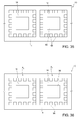
- a solder paste obtained, for example, by particles of tin-silver-copper (SAC) englobed in a flux.
- metallization pads (not illustrated), on which the bumps 46 themselves rest.
- the bumps 46 are formed on the metallization pads arranged on the top surface of the semiconductor body 44.
- the die 42 is then coupled to the intermediate structure 10.
- the die 42 is arranged in the so-called "flip-chip" configuration in such a way that each bump 46 rests on a corresponding pad 40, to which it is temporarily fixed thanks to the adhesive action of the flux.
- additional dice are coupled to the intermediate structure 10, on the corresponding device areas.
- the intermediate structure 10 and the die 42 are subjected to a further thermal treatment, conducted at a temperature, for example, of 260°C and in an environment exposed to a nitrogen flow for carrying out reflow soldering.
- a further thermal treatment conducted at a temperature, for example, of 260°C and in an environment exposed to a nitrogen flow for carrying out reflow soldering.
- each bump 46 is soldered to a corresponding pad 40.
- the gaps present between the bumps 46 are filled, in a per se known manner, with a filling region 48, also known as "underfill".
- a filling region 48 also known as "underfill”.
- the filling region 48 extends between the die surface and the elements underlying it, and thus also on a central portion of the first base region 14.
- the filling region 48 is formed, for example, by a heat-hardening epoxy resin inside which silicone microparticles are dispersed in order to reducing the coefficient of thermal expansion of the resin itself.
- the filling region 48 enables setting-up of a strong mechanical connection between the die 42 and the first base region 14, as well as reduction of the mechanical stress that acts on the soldering in the presence of thermal variations, this stress being due to the difference between the coefficients of thermal expansion of the die 42 and of the first base region 14.
- formation of the filling region 48 may be preceded by an operation of plasma cleaning (not illustrated), of a per se known type, and may be followed, once again in a per se known manner, by a corresponding thermal treatment (not illustrated) at a temperature comprised between 150°C and 170°C, to obtain complete polymerisation of the resin that forms the filling region 48.
- a dielectric region 50 is formed via injection of a corresponding heat-hardening epoxy resin, dispersed in which are silicon microparticles.
- the dielectric region 50 is formed on top of the die 42, as well as on top of the first device area A 1 , i.e., on top of the preliminary contacts 36, of the tracks 38 and of the pads 40.
- the dielectric region 50 also coats the additional dice present on the intermediate structure 10 and the corresponding device areas, without any solution of continuity.
- the plate 8 is removed mechanically from the intermediate structure 10.
- the plate 8 may then be re-used in other processes.
- the supporting structure 2 is removed.
- the first and second supporting layers 4, 6 are dissolved by application of a jet of water at a pressure comprised, for example, between 2 bar and 5 bar, and at the temperature of, for example, 70°C.
- a further thermal treatment may be carried out, for example, at a temperature of 175°C.
- the latter thermal treatment is also known as "post-moulding curing".
- the operations of marking and cutting in such a way as to singulate the intermediate structure 10.
- the first device area A 1 is separated from the other device areas, and thus also the die 42 is separated from the other dice.
- a semiconductor device 51 is thus formed.
- each preliminary contact 36 forms a corresponding contact 53 of sintered material, which not only gives out onto a bottom surface of the package (designated by S 1 in Figure 14 and formed by the first base region 14), but is also provided with a lateral surface, which is exposed, and thus solderable.
- the lateral surface of each contact 53 (designated by S 2 in Figure 14 ) is co-planar with a lateral surface (designated by S 3 in Figure 14 ) of the package region 52.
- the intersection between the lateral surface S 3 of the package region 52 and the bottom surface S 1 of the package region 52 defines an edge E, along which at least part of the contacts 53 extends.
- the package is designated as a whole by P.
- the preliminary contact regions, the preliminary track regions, and the preliminary pad regions are formed by a process of jet printing of the same sinterable ink.
- this ink may comprise nanoparticles of copper or silver dispersed in a solvent.
- the ink may be applied at a temperature of at least 150°C.
- the nanoparticles may have equivalent diameters comprised, for example, between 5 nm and 50 nm.
- a sintering process is carried out, for example, in an oven with a controlled atmosphere at the temperature of 150°C, or in any case at a temperature at least equal to the temperature used during the previous jet-printing process.
- the preliminary contact regions 60, the preliminary track regions 62, and the preliminary pad regions 64 form, respectively, the preliminary contacts (here designated by 66), the tracks (here designated by 68), and the pads (here designated by 70).
- the preliminary contacts 66, the tracks 68, and the pads 70 thus form a single sintered region, which has a thickness comprised, for example, between 10 ⁇ m and 30 ⁇ m.
- the preliminary contact regions 30, and thus the first device area A 1 are formed directly on the first supporting layer 4, with which they are in direct contact.
- the preliminary track regions and the preliminary pad regions are not instead formed.
- the preliminary contact regions 30 are formed, once again by a process of silk-screen printing, by the sintering paste mentioned with reference to Figure 5 , which, as has been said, may comprise, for example, copper and tin microparticles, dispersed in an epoxy resin, or else may comprise, once again purely by way of example, copper microparticles coated with silver and dispersed in a solvent.
- the first device area A 1 further comprises a preliminary die pad 54, which extends over the first supporting layer 4, with which it is in direct contact. Furthermore, the preliminary die pad 54 is surrounded, at a distance, by the preliminary contact regions 30.
- the preliminary die pad 54 has, for example, a square shape; the preliminary contact regions 30 are arranged along the sides of a square, arranged inside which is the square shape defined by the preliminary die pad 54.
- the preliminary die pad 54 is of the same sintering paste as that with which the preliminary contact regions 30 are formed.
- the intermediate structure 10 is subjected to a thermal treatment, of the same type as the one described with reference to Figure 7 , which, as has been said, depends upon the type of sintering paste adopted.
- each preliminary contact region 30 forms a corresponding preliminary contact 36.
- the preliminary die pad 54 forms a die pad 56.
- the preliminary contacts 36 and the die pad 56 may have thicknesses comprised, for example, between 15 ⁇ m and 50 ⁇ m.
- a preliminary gluing region 74 formed by a conductive glue of a per se known type.
- the die (here designated by 72) is arranged on the preliminary gluing region 74.
- the die 72 comprises the semiconductor body (here designated by 75) and a bottom dielectric region 77, made, for example, of silicon dioxide. Further, the bottom dielectric region 77 contacts the preliminary gluing region 74.
- a thermal treatment of the intermediate structure 10 is carried out, for example, at 170°C and with a duration of two hours, in order to harden the preliminary gluing region 74.
- the preliminary gluing region 74 forms a gluing region 76, arranged between the die 72 and the die pad 56.
- a process of plasma cleaning of the preliminary contacts 36 may be carried out in a per se known manner using as reactive gas a mixture of nitrogen (96%) and hydrogen (4%). This operation is not illustrated.
- the die 72 is electrically connected to the preliminary contacts 36, by corresponding conductive wires 78, made, for example, of silver.
- Each conductive wire 78 contacts a corresponding preliminary contact 36, with which it forms a corresponding wire bonding.
- the wire bondings are formed at a maximum temperature of approximately 200°C.
- the aforementioned dielectric region 50 is formed on the die 72, as well as on the first device area A 1 , i.e., on the preliminary contacts 36.
- the dielectric region 50 also coats the additional dice present in the intermediate structure 10 and the corresponding device areas, without any solution of continuity.
- the supporting structure 2 is removed.
- the first and second supporting layers 4, 6 are dissolved by application of a jet of water at a pressure comprised, for example, between 2 bar and 5 bar, and at the temperature of, for example, 70°C.
- a further thermal treatment may be carried out, for example, at the temperature of 175°C; the latter thermal treatment functions as "post-moulding curing".
- the operations of marking and cutting are then carried out, in a per se known manner, in such a way as to singulate the intermediate structure 10 and form the semiconductor device 51.
- the package P illustrated in Figure 26 is of the same type as that illustrated in Figure 14 , but the contacts 53 are electrically connected to the die 72 by wire bonds.
- the bottom surface S 1 of the package P is formed in part by the die pad 56 and in part by the package region 52.
- the die (illustrated in Figure 27 , where it is designated by 82) comprises, in addition to the semiconductor body 75, a bottom metallization 84.
- the manufacturing process envisages, after carrying out the operations represented in Figure 17 , arranging the die 82 so that the bottom metallization 84 contacts the preliminary die pad 54.
- the aforementioned sintering process is carried out, following upon which the preliminary contact regions 30 form corresponding preliminary contacts 36, whereas the preliminary die pad 54 forms the die pad 56.
- the die 82 remains fixed to the die pad 56.
- a process of plasma cleaning of the preliminary contacts 36 may be carried out in a per se known manner using as reactive gas a mixture of nitrogen (96%) and hydrogen (4%). This operation is not illustrated. Then, the operations described previously with reference to Figures 22-26 are carried out.
- the preliminary contact regions and the preliminary die pad are formed by process of jet printing of a sinterable ink, of the same type as the one described with reference to Figure 15 .
- a sintering process is carried out, for example in an oven with a controlled atmosphere at the temperature of 150°C, or in any case at a temperature at least equal to the temperature used during the previous jet-printing process.
- the preliminary contact regions 90 and the preliminary die pad 94 form, respectively, the preliminary contacts (here designated by 96) and the die pad (here designated by 98).
- the preliminary contacts 96 and the die pad 98 have a thickness comprised, for example, between 10 ⁇ m and 30um.
- the preliminary contact regions 30, and consequently the preliminary contacts 36 it is further possible for the preliminary contact regions 30, and consequently the preliminary contacts 36, to have heights such that the contacts 53 give out, not only onto the bottom surface S 1 of the package P, but also onto a top surface (designated by S 4 in Figure 31 ) of the package region 52, i.e., onto the top surface of the package itself.
- the tracks 38 extend, instead, as described previously.
- a three-dimensional structure 100 which includes, in addition to the semiconductor device 51, at least one additional device 102, which comprises a respective semiconductor body 104, a respective metallization region 106, and a plurality of respective contacts 108.
- the metallization region 106 is arranged between the contacts 108 and the semiconductor body 104 of the additional device 102.
- the contacts 108 of the additional device 102 contact the top portions of corresponding contacts 53 of the semiconductor device 51.
- Figure 31 refers, by way of example, to the case where the die 42 is arranged in flip-chip configuration, this type of package may be implemented also in the case where the die is connected to the contacts by wire bonds, as well as in the absence of the first base region 14.
- the present manufacturing method makes it possible to prescind from the need of having lead-frame strips.
- the packages formed with the present manufacturing method are characterized by lower weights, on account of the lightness of the sintered material, as well as on account of a smaller thickness.
- the pitch of the contacts may be comprised between 200 ⁇ m and 350 ⁇ m.
- the preliminary contact regions 30 are formed, as described with reference to Figure 5 , i.e., by a process of silk-screen printing. Furthermore, with this process of silk-screen printing, the preliminary die pad 54 is likewise formed on the main body 15 of the first base region 14.
- the preliminary contact regions 30 are thus of the same type as what has been described with reference to Figure 6 and present the same advantages, which are guaranteed precisely by use of the first base region 14, irrespective of the type of methodology used for applying the sintering paste.
- a subsequent sintering treatment of the same type as the one described with reference to Figure 18 , leads to formation of the preliminary contacts 36 and of the die pad 56, as illustrated in Figure 33 .
- the operations described previously with reference to Figures 19-28 may be carried out. In this way, there is obtained, for example, the semiconductor device 51 illustrated in Figure 34 .
- the preliminary die pad is formed on the first base region 14
- the jet print leads to formation of the preliminary contact regions and of the preliminary die pad (designated, respectively, by 90 and 94), the latter being arranged on the first base region 14.
- a subsequent sintering process of the same type as the one described with reference to Figure 30 leads to formation of the preliminary contacts 96 and of the die pad 98, as illustrated in Figure 36 .
- the operations described previously with reference to Figures 19-28 may be carried out.
- the present manufacturing method may further be used for forming packages different from QFN packages, such as, for example, the packages of the land-grid-array (LGA) type.
- packages different from QFN packages such as, for example, the packages of the land-grid-array (LGA) type.
- this may be absent. Furthermore, instead of reflow soldering, it is possible to implement, for example, thermosonic bonding.
- the gluing region 76 this may not be present. In this case, it is, for example, possible to apply on the bottom dielectric region 77 of the die 72 a bi-adhesive layer (not illustrated), whether conductive or insulating. Next, the die 72 is fixed to the die pad 56 thanks to the action of the bi-adhesive layer.
- the supporting structure 2 instead of being formed by the first supporting layer 4 and the second supporting layer 6, it may be formed by just one watersoluble layer (not illustrated).
- the soluble layer is formed, for example, by injectable polyvinyl acetate, or else by a bio-material.
- the soluble layer may include glass fibre or silicon microparticles.
- the soluble layer may have the following characteristics: thickness comprised between 0.2 mm and 1.0 mm; elastic modulus of 10 GPa at room temperature and 5 GPa RT; coefficient of cubic expansion lower than 200 ppm; temperature of vitreous transition higher than 150°C; melting point higher than 200°C; and complete solubility in water at 80°C (except for the glass-fibre/silicon microparticles).
Landscapes
- Encapsulation Of And Coatings For Semiconductor Or Solid State Devices (AREA)
- Physics & Mathematics (AREA)
- Geometry (AREA)
- Structures Or Materials For Encapsulating Or Coating Semiconductor Devices Or Solid State Devices (AREA)
- Die Bonding (AREA)
- Engineering & Computer Science (AREA)
- Microelectronics & Electronic Packaging (AREA)
- Wire Bonding (AREA)
Abstract
Description
- The present invention relates to a process for manufacturing a package for a surface-mount semiconductor device, as well as to the corresponding semiconductor device.
- As is known, semiconductor devices, such as, for example, integrated circuits and MEMS devices, are encapsulated within corresponding packages, which perform functions of protection and interfacing with the outside world. For instance, there are known packages that enable so-called surface mounting on a printed-circuit board (PCB).
- In greater detail, surface-mount packages comprise, for example, the so-called packages of a "quad-flat no-leads" (QFN) type, also known as "micro-lead frame" (MLF) or "small-outline no-leads" (SON) packages.
- In general, with reference, for example, to a package of a QFN type, it comprises a region of resin, englobed inside which is a lead frame, which in turn forms at least one array of terminals that give out onto a bottom surface of the package. An example of process for manufacturing a package comprising a lead frame is described in the document No.
US 2005/0116321 . - Traditionally, lead frames are manufactured in strips, which are subsequently used in the manufacturing processes. This being said, even though the technologies that enable production of packages starting from lead-frame strips are by now well consolidated, they are still relatively costly. Further, the packages thus obtained have relatively high weights.
- The aim of the present invention is thus to provide a manufacturing process for a package for a semiconductor device, which will overcome at least in part the drawbacks of the known art.
- According to the present invention, a manufacturing process and a semiconductor device are provided, as defined respectively in
claims 1 and 10. - For a better understanding of the present invention, preferred embodiments thereof are now described purely by way of non-limiting example and with reference to the attached drawings, wherein:
-
Figures 1-3 are schematic cross-sectional views of portions of an intermediate structure, during successive steps of an embodiment of the present manufacturing process; -
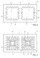
Figures 4, 5 , and7 are schematic top plan views of portions of an intermediate structure, during successive steps of an embodiment of the present manufacturing process; -
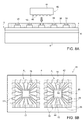
Figure 6 is a schematic illustration of a portion of a cross-section of the intermediate structure illustrated inFigure 5 , taken along a line of section VI-VI represented inFigure 5 ; -
Figure 8a is a schematic lateral view of a portion of an intermediate structure, during a step of an embodiment of the manufacturing process; -
Figure 8b is a schematic top plan view of a portion of an intermediate structure, during the same step illustrated inFigure 8a ; -
Figures 9 and 10 are schematic lateral views of portions of the intermediate structure, during successive steps of an embodiment of the manufacturing process; -
Figures 11-14 are schematic cross-sectional views of portions of an intermediate structure, during successive steps of an embodiment of the manufacturing process; -
Figures 15 and 16 are schematic top plan views of portions of an intermediate structure, during successive steps of an embodiment of the present manufacturing process; -
Figures 17 and 18 are schematic top plan views of portions of an intermediate structure, during successive steps of an embodiment of the present manufacturing process; -
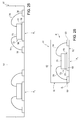
Figures 19-25 are schematic cross-sectional views of portions of an intermediate structure, during successive steps of an embodiment of the manufacturing process; -
Figures 26 and34 are schematic cross-sectional views of semiconductor devices; -
Figures 27 and 28 are schematic cross-sectional views of portions of an intermediate structure, during successive steps of an embodiment of the manufacturing process; -
Figures 29 and 30 are schematic top plan views of portions of an intermediate structure, during successive steps of an embodiment of the present manufacturing process; -
Figure 31 is a schematic illustration of a cross-section of a three-dimensional electronic structure; -
Figures 32 and 33 are schematic top plan views of portions of an intermediate structure, during successive steps of an embodiment of the present manufacturing process; and -
Figures 35 and 36 are schematic top plan views of portions of an intermediate structure, during successive steps of an embodiment of the present manufacturing process. -
Figure 1 shows a supportingstructure 2 of a watersoluble type, which comprises afirst layer 4 and asecond layer 6, referred to hereinafter as "first supportinglayer 4" and "second supportinglayer 6".Figure 1 , as on the other hand also the subsequent figures, is not in scale. - The first and second supporting
layers layer 4 is formed, for example, by a film of polyvinyl acetate (PVA) or polyvinyl pyrrolidone (PVP), which may have a thickness comprised, for example, between 10 µm and 30 µm. Thesecond layer 6 is formed, for example, by a pressure-sensitive adhesive film (PSA film) soluble in water, which may have a thickness comprised, for example, between 20 µm and 30 µm. More in particular, the second supportinglayer 6 may be formed, for example, by a gel containing a mixture of polyvinyl acetate and sodium silicate. - As illustrated once again in
Figure 1 , according to the present manufacturing method, the supportingstructure 2 is mechanically coupled to aplate 8, which is made, for example, of steel and has a thickness comprised, for instance, between 0.2 mm and 0.5 mm, for functioning as stiffener. - More in particular, the supporting
structure 2 is laminated; i.e., it is arranged on theplate 8 in such a way that the second supportinglayer 6 contacts theplate 8. Lamination is carried out, for example, in a pressurized oven, with a pressure of 5 bar and a temperature of 200°C, for eliminating the air bubbles that may develop following upon heating of the second supportinglayer 6. In this way, the first supportinglayer 4 is glued to theplate 8, thanks to the action of gluing performed by the second supportinglayer 6, as illustrated inFigure 2 . There is thus formed anassembly 10, i.e., an intermediate structure, which has a thickness comprised, for example, between 0.23 mm and 0.56 mm. - Next, as illustrated in
Figure 3 , formed on top of the first supportinglayer 4 is athird layer 12 of dielectric material, such as, for example, an acrylic adhesive resin curable with ultraviolet radiation. Thethird layer 12 may be formed in a per se known manner, for example by silk-screen printing and subsequent curing. Further, thethird layer 12 has a thickness comprised, for example, between 10 µm and 30 µm. - As illustrated also in
Figure 4 , thethird layer 12 forms a plurality of dielectric regions. In particular, illustrated inFigure 4 are a firstdielectric region 14 and a seconddielectric region 16, referred to hereinafter as "first andsecond base regions second base regions - The first and
second base regions second base regions Figure 4 , the teeth of thefirst base region 14 are designated by 19, whereas the teeth of thesecond base region 16 are designated by 21. - In turn, the teeth define a plurality of recesses, open at the top and delimited at the bottom by the first supporting
layer 4. InFigure 4 , the recesses defined by thefirst base region 14 are designated by 23, whereas the recesses defined by thesecond base region 16 are designated by 25. - In what follows, for brevity, the operations of the present manufacturing method are described with reference to the portion of
intermediate structure 10 including thefirst base region 14, except where otherwise specified. - This said, as illustrated in
Figure 5 , there are subsequently formed a plurality ofpreliminary contact regions 30, a plurality ofpreliminary track regions 32, and a plurality ofpreliminary pad regions 34, of a conductive type. - In detail, the
preliminary contact regions 30, thepreliminary track regions 32, and thepreliminary pad regions 34 are formed, by a process of silk-screen printing, from the same sintering paste of a per se known type; for example, the sintering paste may be formed by so-called "transient-phase liquid sintering" (TPLS). - In greater detail, the sintering paste may comprise metal microparticles, which have equivalent diameters comprised, for example, between 10 µm and 30 µm.
- In even greater detail, the sintering paste may comprise, for example, copper and tin microparticles, bonded by an epoxy resin. In this case, if arranged in an environment at a temperature of 220°C and with low oxygen content, the microparticles form a copper-tin intermetal compound. Once again by way of example, the sintering paste may likewise be formed by copper microparticles coated with silver and dispersed in a solvent. In this case, if the sintering paste is heated up to 170°C, the solvent evaporates.
- In greater detail, each
preliminary contact region 30 is formed within acorresponding recess 19 of thefirst base region 14 for contacting the underlying first supportinglayer 4. - As illustrated in greater detail in
Figure 6 , eachpreliminary contact region 30 comprises a bottom portion, which contacts the first supportinglayer 4 and extends between a corresponding pair ofteeth 19, and a top portion, which overlies the bottom portion and extends laterally until it partially overlies also the aforementioned pair ofteeth 19. In particular, the top portion comprises a first lateral sub-portion and a second lateral sub-portion, which extend, respectively, on the two teeth of the aforementioned pair ofteeth 19. Each of the first and second lateral sub-portions may have a width, for example, of 0.1 mm. In this way, thepreliminary contact regions 30 maintain the respective positions within theintermediate structure 10, also when they are subjected to stresses induced by removal of the underlying layers (as described hereinafter), or else to the thermo-mechanical stresses caused by the difference between the coefficients of thermal expansion (CTE) of thepreliminary contact regions 30 and of the surrounding elements. - As regards the
preliminary pad regions 34, without this implying any loss of generality, they are equal in number to thepreliminary contact regions 30. Furthermore, thepreliminary pad regions 34 are formed on top of thefirst base region 14, with which they are in direct contact. In particular, without this implying any loss of generality, thepreliminary contact regions 30 are arranged along the sides of a imaginary square, arranged in a central portion of themain body 15 of thefirst base region 14. - As regards the
preliminary track regions 32, without this implying any loss of generality, they are equal in number to thepreliminary contact regions 30. Furthermore, thepreliminary track regions 32 are formed on top of thefirst base region 14, with which they are in direct contact. In particular, eachpreliminary track region 32 is arranged between a correspondingpreliminary pad region 34 and a correspondingpreliminary contact region 30, with which it is in direct contact. Consequently, thepreliminary track regions 32 form a sort of plurality of arms directed to a first approximation radially, which guarantee electrical continuity between eachpreliminary pad region 34 and the correspondingpreliminary contact region 30. - Next, as illustrated in
Figure 7 , a sintering process is carried out in a per se known manner. In detail, theintermediate structure 10 is subjected to a thermal treatment. For instance, in the case where the sintering paste contains copper and tin microparticles, the thermal treatment may envisage a gradual rise in temperature from 25°C to 215°C, in thirty minutes, the temperature of 215°C being subsequently maintained for seventy-five minutes. Furthermore, the thermal treatment may be conducted in an environment with a controlled atmosphere having a low oxygen content (for example, less than 200 ppm), which may be obtained thanks to a continuous flow of nitrogen. Alternatively, if the sintering paste contains copper microparticles coated with silver, the thermal treatment may have a duration of thirty minutes and be carried out at a temperature of 170°C. - At the end of sintering, each
preliminary contact region 30 forms a correspondingpreliminary contact 36. Further, eachpreliminary track region 32 forms a correspondingtrack 38, while eachpreliminary pad region 34 forms acorresponding pad 40. Thepreliminary contacts 36, thetracks 38, and thepads 40 thus form a single sintered region, which may have a thickness comprised, for example, between 10 µm and 50 µm, and is referred to hereinafter also as "first device area A1".Figure 7 , in addition to the first device area A1, also illustrates a second device area A2, formed on thesecond base region 16. In a per se known manner, sintering is irreversible; i.e., even increasing the temperature again up to 270°C, the material does not re-melt. - Next, a
die 42 is provided of a per se known manner type, illustrated inFigure 8a . - The
die 42 includes asemiconductor body 44 and a plurality ofcontacts 46, which are known as "bumps" 46 and are formed by a solder paste, obtained, for example, by particles of tin-silver-copper (SAC) englobed in a flux. Arranged between thebumps 46 and thesemiconductor body 44 are metallization pads (not illustrated), on which thebumps 46 themselves rest. In particular, thebumps 46 are formed on the metallization pads arranged on the top surface of thesemiconductor body 44. - As illustrated once again in
Figure 8a and inFigure 8b , thedie 42 is then coupled to theintermediate structure 10. In particular, thedie 42 is arranged in the so-called "flip-chip" configuration in such a way that eachbump 46 rests on acorresponding pad 40, to which it is temporarily fixed thanks to the adhesive action of the flux. Even though not illustrated or described any further, additional dice are coupled to theintermediate structure 10, on the corresponding device areas. - Next, as illustrated in
Figure 9 , theintermediate structure 10 and the die 42 are subjected to a further thermal treatment, conducted at a temperature, for example, of 260°C and in an environment exposed to a nitrogen flow for carrying out reflow soldering. In practice, at the end of the soldering process, eachbump 46 is soldered to acorresponding pad 40. - Next, as illustrated in
Figure 10 , the gaps present between thebumps 46 are filled, in a per se known manner, with a fillingregion 48, also known as "underfill". In practice, if the surface defined by the metallization pads (not illustrated) on which thebumps 46 are arranged is referred to as "die surface", the fillingregion 48 extends between the die surface and the elements underlying it, and thus also on a central portion of thefirst base region 14. - The filling
region 48 is formed, for example, by a heat-hardening epoxy resin inside which silicone microparticles are dispersed in order to reducing the coefficient of thermal expansion of the resin itself. In this way, the fillingregion 48 enables setting-up of a strong mechanical connection between the die 42 and thefirst base region 14, as well as reduction of the mechanical stress that acts on the soldering in the presence of thermal variations, this stress being due to the difference between the coefficients of thermal expansion of thedie 42 and of thefirst base region 14. - In greater detail, formation of the filling
region 48 may be preceded by an operation of plasma cleaning (not illustrated), of a per se known type, and may be followed, once again in a per se known manner, by a corresponding thermal treatment (not illustrated) at a temperature comprised between 150°C and 170°C, to obtain complete polymerisation of the resin that forms the fillingregion 48. - Next, as illustrated in
Figure 11 , adielectric region 50 is formed via injection of a corresponding heat-hardening epoxy resin, dispersed in which are silicon microparticles. In particular, thedielectric region 50 is formed on top of the die 42, as well as on top of the first device area A1, i.e., on top of thepreliminary contacts 36, of thetracks 38 and of thepads 40. Albeit not illustrated, thedielectric region 50 also coats the additional dice present on theintermediate structure 10 and the corresponding device areas, without any solution of continuity. - Next, as illustrated in
Figure 12 , theplate 8 is removed mechanically from theintermediate structure 10. Theplate 8 may then be re-used in other processes. - Next, as illustrated in
Figure 13 , the supportingstructure 2 is removed. In particular, the first and second supportinglayers - Next, albeit not illustrated, a further thermal treatment may be carried out, for example, at a temperature of 175°C. The latter thermal treatment is also known as "post-moulding curing".
- As illustrated in
Figure 14 , there are then carried out, in a per se known manner, the operations of marking and cutting, in such a way as to singulate theintermediate structure 10. In other words, the first device area A1 is separated from the other device areas, and thus also thedie 42 is separated from the other dice. Asemiconductor device 51 is thus formed. - Following upon the cutting operations, the
dielectric region 50 forms apackage region 52, which covers thedie 42. Furthermore, in the example illustrated inFigure 14 , cutting is carried out in such a way that eachpreliminary contact 36 forms acorresponding contact 53 of sintered material, which not only gives out onto a bottom surface of the package (designated by S1 inFigure 14 and formed by the first base region 14), but is also provided with a lateral surface, which is exposed, and thus solderable. In greater detail, the lateral surface of each contact 53 (designated by S2 inFigure 14 ) is co-planar with a lateral surface (designated by S3 inFigure 14 ) of thepackage region 52. Furthermore, the intersection between the lateral surface S3 of thepackage region 52 and the bottom surface S1 of thepackage region 52 defines an edge E, along which at least part of thecontacts 53 extends. InFigure 14 , the package is designated as a whole by P. - In practice, the cutting operation illustrated in
Figure 14 leads, without this implying any loss of generality, to formation of a device with a package of the quad-flat no-leads (QFN) type. - According to a variant illustrated in
Figure 15 , the preliminary contact regions, the preliminary track regions, and the preliminary pad regions (designated, respectively, by 60, 62, and 64) are formed by a process of jet printing of the same sinterable ink. For instance, this ink may comprise nanoparticles of copper or silver dispersed in a solvent. Further, the ink may be applied at a temperature of at least 150°C. In general, the nanoparticles may have equivalent diameters comprised, for example, between 5 nm and 50 nm. - Next, as illustrated in
Figure 16 , a sintering process is carried out, for example, in an oven with a controlled atmosphere at the temperature of 150°C, or in any case at a temperature at least equal to the temperature used during the previous jet-printing process. - Following upon sintering, the
preliminary contact regions 60, thepreliminary track regions 62, and thepreliminary pad regions 64 form, respectively, the preliminary contacts (here designated by 66), the tracks (here designated by 68), and the pads (here designated by 70). Thepreliminary contacts 66, thetracks 68, and thepads 70 thus form a single sintered region, which has a thickness comprised, for example, between 10 µm and 30 µm. - Next, the operations described previously with reference to
Figures 8a, 8b and 9-14 are carried out. - According to a different embodiment, illustrated in
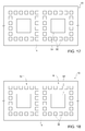
Figure 17 , thepreliminary contact regions 30, and thus the first device area A1, are formed directly on the first supportinglayer 4, with which they are in direct contact. The preliminary track regions and the preliminary pad regions are not instead formed. - In particular, the
preliminary contact regions 30 are formed, once again by a process of silk-screen printing, by the sintering paste mentioned with reference toFigure 5 , which, as has been said, may comprise, for example, copper and tin microparticles, dispersed in an epoxy resin, or else may comprise, once again purely by way of example, copper microparticles coated with silver and dispersed in a solvent. - The first device area A1 further comprises a
preliminary die pad 54, which extends over the first supportinglayer 4, with which it is in direct contact. Furthermore, thepreliminary die pad 54 is surrounded, at a distance, by thepreliminary contact regions 30. In particular, in top plan view thepreliminary die pad 54 has, for example, a square shape; thepreliminary contact regions 30 are arranged along the sides of a square, arranged inside which is the square shape defined by thepreliminary die pad 54. Thepreliminary die pad 54 is of the same sintering paste as that with which thepreliminary contact regions 30 are formed. - Next, as illustrated in
Figure 18 , a sintering process is carried out in a per se known manner. - In detail, the
intermediate structure 10 is subjected to a thermal treatment, of the same type as the one described with reference toFigure 7 , which, as has been said, depends upon the type of sintering paste adopted. - At the end of the sintering process, each
preliminary contact region 30 forms a correspondingpreliminary contact 36. Further, thepreliminary die pad 54 forms adie pad 56. Thepreliminary contacts 36 and thedie pad 56 may have thicknesses comprised, for example, between 15 µm and 50 µm. - Next, as illustrated in
Figure 19 , formed on thedie pad 56 is apreliminary gluing region 74, formed by a conductive glue of a per se known type. - Then, as illustrated in
Figure 20 , the die (here designated by 72) is arranged on thepreliminary gluing region 74. Thedie 72 comprises the semiconductor body (here designated by 75) and a bottomdielectric region 77, made, for example, of silicon dioxide. Further, the bottomdielectric region 77 contacts thepreliminary gluing region 74. - Next, as illustrated in
Figure 21 , a thermal treatment of theintermediate structure 10 is carried out, for example, at 170°C and with a duration of two hours, in order to harden thepreliminary gluing region 74. Following upon the latter thermal treatment, thepreliminary gluing region 74 forms a gluingregion 76, arranged between the die 72 and thedie pad 56. - Then, a process of plasma cleaning of the
preliminary contacts 36 may be carried out in a per se known manner using as reactive gas a mixture of nitrogen (96%) and hydrogen (4%). This operation is not illustrated. - Next, as illustrated in
Figure 22 , thedie 72 is electrically connected to thepreliminary contacts 36, by correspondingconductive wires 78, made, for example, of silver. Eachconductive wire 78 contacts a correspondingpreliminary contact 36, with which it forms a corresponding wire bonding. The wire bondings are formed at a maximum temperature of approximately 200°C. - Next, as illustrated in
Figure 23 , the aforementioneddielectric region 50 is formed on thedie 72, as well as on the first device area A1, i.e., on thepreliminary contacts 36. Thedielectric region 50 also coats the additional dice present in theintermediate structure 10 and the corresponding device areas, without any solution of continuity. - Then, as illustrated in
Figure 24 , theplate 8 is removed from theintermediate structure 10. - Next, as illustrated in
Figure 25 , the supportingstructure 2 is removed. In particular, the first and second supportinglayers - Then, even though not illustrated, a further thermal treatment may be carried out, for example, at the temperature of 175°C; the latter thermal treatment functions as "post-moulding curing".
- As illustrated in
Figure 26 , the operations of marking and cutting are then carried out, in a per se known manner, in such a way as to singulate theintermediate structure 10 and form thesemiconductor device 51. - In particular, without this implying any loss of generality, the package P illustrated in
Figure 26 is of the same type as that illustrated inFigure 14 , but thecontacts 53 are electrically connected to the die 72 by wire bonds. For completeness, in this case the bottom surface S1 of the package P is formed in part by thedie pad 56 and in part by thepackage region 52. - According to a different embodiment, the die (illustrated in
Figure 27 , where it is designated by 82) comprises, in addition to thesemiconductor body 75, abottom metallization 84. In this case, the manufacturing process envisages, after carrying out the operations represented inFigure 17 , arranging the die 82 so that thebottom metallization 84 contacts thepreliminary die pad 54. Next, as illustrated inFigure 28 , the aforementioned sintering process is carried out, following upon which thepreliminary contact regions 30 form correspondingpreliminary contacts 36, whereas thepreliminary die pad 54 forms thedie pad 56. Furthermore, on account of the sintering process, the die 82 remains fixed to thedie pad 56. - Next, a process of plasma cleaning of the
preliminary contacts 36 may be carried out in a per se known manner using as reactive gas a mixture of nitrogen (96%) and hydrogen (4%). This operation is not illustrated. Then, the operations described previously with reference toFigures 22-26 are carried out. - According to a variant, illustrated in
Figure 29 , the preliminary contact regions and the preliminary die pad (designated, respectively, by 90 and 94) are formed by process of jet printing of a sinterable ink, of the same type as the one described with reference toFigure 15 . - Next, as illustrated in
Figure 30 , a sintering process is carried out, for example in an oven with a controlled atmosphere at the temperature of 150°C, or in any case at a temperature at least equal to the temperature used during the previous jet-printing process. - Following upon the sintering operation, the
preliminary contact regions 90 and thepreliminary die pad 94 form, respectively, the preliminary contacts (here designated by 96) and the die pad (here designated by 98). Thepreliminary contacts 96 and thedie pad 98 have a thickness comprised, for example, between 10 µm and 30um. - Next, the operations described previously with reference to
Figures 19-28 are carried out. - Irrespective of whether the die is arranged in a flip-chip configuration or else is connected to the contacts by wire bonds, it is further possible for the
preliminary contact regions 30, and consequently thepreliminary contacts 36, to have heights such that thecontacts 53 give out, not only onto the bottom surface S1 of the package P, but also onto a top surface (designated by S4 inFigure 31 ) of thepackage region 52, i.e., onto the top surface of the package itself. Thetracks 38 extend, instead, as described previously. - As illustrated once again in
Figure 31 , it is thus possible to form a three-dimensional structure 100, which includes, in addition to thesemiconductor device 51, at least oneadditional device 102, which comprises arespective semiconductor body 104, arespective metallization region 106, and a plurality ofrespective contacts 108. For instance, themetallization region 106 is arranged between thecontacts 108 and thesemiconductor body 104 of theadditional device 102. Further, thecontacts 108 of theadditional device 102 contact the top portions ofcorresponding contacts 53 of thesemiconductor device 51. Even thoughFigure 31 refers, by way of example, to the case where thedie 42 is arranged in flip-chip configuration, this type of package may be implemented also in the case where the die is connected to the contacts by wire bonds, as well as in the absence of thefirst base region 14. - From what has been described and illustrated previously, the advantages that the present solution affords emerge clearly.
- In particular, the present manufacturing method makes it possible to prescind from the need of having lead-frame strips. Furthermore, the packages formed with the present manufacturing method are characterized by lower weights, on account of the lightness of the sintered material, as well as on account of a smaller thickness. In this connection, in the case of a flip-chip arrangement, it is possible to form packages having thicknesses in the region of 0.2 mm. Again, the pitch of the contacts may be comprised between 200 µm and 350 µm.
- Finally, it is clear that modifications and variations may be made to what has been described and illustrated herein, without thereby departing from the scope of the present invention, as defined in the annexed claims.
- For instance, as illustrated in
Figure 32 , it is possible to use thethird layer 12, and thus the aforementioned first andsecond base regions Figure 4 have been carried out, thepreliminary contact regions 30 are formed, as described with reference toFigure 5 , i.e., by a process of silk-screen printing. Furthermore, with this process of silk-screen printing, thepreliminary die pad 54 is likewise formed on themain body 15 of thefirst base region 14. Thepreliminary contact regions 30 are thus of the same type as what has been described with reference toFigure 6 and present the same advantages, which are guaranteed precisely by use of thefirst base region 14, irrespective of the type of methodology used for applying the sintering paste. A subsequent sintering treatment, of the same type as the one described with reference toFigure 18 , leads to formation of thepreliminary contacts 36 and of thedie pad 56, as illustrated inFigure 33 . Next, the operations described previously with reference toFigures 19-28 may be carried out. In this way, there is obtained, for example, thesemiconductor device 51 illustrated inFigure 34 . - As illustrated in
Figure 35 , also in the case where the preliminary die pad is formed on thefirst base region 14, it is possible for it to be formed by a jet-printing process, with the characteristics described previously. In this case, the jet print leads to formation of the preliminary contact regions and of the preliminary die pad (designated, respectively, by 90 and 94), the latter being arranged on thefirst base region 14. A subsequent sintering process of the same type as the one described with reference toFigure 30 leads to formation of thepreliminary contacts 96 and of thedie pad 98, as illustrated inFigure 36 . Next, the operations described previously with reference toFigures 19-28 may be carried out. - In general, the present manufacturing method may further be used for forming packages different from QFN packages, such as, for example, the packages of the land-grid-array (LGA) type.
- As regards the filling
region 48, this may be absent. Furthermore, instead of reflow soldering, it is possible to implement, for example, thermosonic bonding. - As regards the gluing
region 76, this may not be present. In this case, it is, for example, possible to apply on the bottomdielectric region 77 of the die 72 a bi-adhesive layer (not illustrated), whether conductive or insulating. Next, thedie 72 is fixed to thedie pad 56 thanks to the action of the bi-adhesive layer. - As regards the supporting
structure 2, instead of being formed by the first supportinglayer 4 and the second supportinglayer 6, it may be formed by just one watersoluble layer (not illustrated). In this case, the soluble layer is formed, for example, by injectable polyvinyl acetate, or else by a bio-material. Furthermore, the soluble layer may include glass fibre or silicon microparticles. - In greater detail, the soluble layer may have the following characteristics: thickness comprised between 0.2 mm and 1.0 mm; elastic modulus of 10 GPa at room temperature and 5 GPa RT; coefficient of cubic expansion lower than 200 ppm; temperature of vitreous transition higher than 150°C; melting point higher than 200°C; and complete solubility in water at 80°C (except for the glass-fibre/silicon microparticles).
Claims (18)
- A process for manufacturing a surface-mount electronic device, comprising the steps of:- forming a plurality of preliminary contact regions (30; 60; 90) of a sinterable material on a supporting structure (2);- mechanically coupling a die (42; 72; 82) including a semiconductor body (44; 75) to the supporting structure (2); and- sintering said sinterable material, in such a way that each preliminary contact region (30; 60; 90) forms a corresponding sintered preliminary contact (36; 66; 96).
- The process according to claim 1, wherein said supporting structure (2) is of a soluble type, said process further comprising the steps of:- coating the die (42; 72; 82) and the preliminary contact regions (30; 60; 90) with a dielectric coating region (50); and then- removing said supporting structure (2) by a jet of liquid.
- The process according to claim 2, further comprising the step of cutting said dielectric coating region (50); and wherein said cutting step is performed in such a way as to cut also portions of the sintered preliminary contacts (36; 66; 96) in such a way that each sintered preliminary contact (36; 66; 96) forms a corresponding contact (53) having a lateral surface (S2) exposed.
- The process according to any one of claims 1 to 3, further comprising the step of forming at least one insulating region (14) on the supporting structure (2) so that said insulating region (14) forms a plurality of lateral teeth (19), which delimit corresponding recesses (23); and wherein said step of forming a plurality of preliminary contact regions (30; 60; 90) comprises forming said plurality of preliminary contact regions (30; 60; 90) so that each preliminary contact region (30; 60; 90) extends into a corresponding recess (23) and partially overlies the insulating region (14).
- The process according to claim 4, further comprising the steps of:- forming on the insulating region (14) a plurality of preliminary tracks (32; 62) and preliminary pads (34; 64) of said sinterable material; and- electrically connecting the semiconductor body (44; 75) to said preliminary pads (34; 64).
- The process according to any one of claims 1 to 3, further comprising the steps of:- forming a preliminary die pad (54; 94) of said sinterable material on the supporting structure (2);- sintering the preliminary die pad (54; 94) so as to form a sintered die pad (56; 98) and then fixing said die (72) to the sintered die pad (56; 98); and- electrically connecting the semiconductor body (75) to said sintered preliminary contacts (36; 66; 96).
- The process according to any one of claims 1 to 3, further comprising the steps of:- forming a preliminary die pad (54; 94) of said sinterable material on the supporting structure (2);- arranging the die (82) on the preliminary die pad (54; 94) so that a metallization region (84) of the die (82) contacts the preliminary die pad (54; 94); and then- sintering the preliminary die pad (54; 94) so as to form a sintered die pad (56; 98); and- electrically connecting the semiconductor body (75) to said sintered preliminary contacts (36; 66; 96).
- The process according to claim 6 or claim 7, further comprising the step of forming at least one insulating region (14) on the supporting structure (2) so that said insulating region (14) forms a plurality of lateral teeth (19), which delimit corresponding recesses (23); and wherein said step of forming a plurality of preliminary contact regions (30; 60; 90) comprises forming said plurality of preliminary contact regions (30; 60; 90) so that each preliminary contact region (30; 60; 90) extends into a corresponding recess (23) and partially overlies the insulating region (14); and wherein said step of forming a preliminary die pad (54; 94) comprises forming said preliminary die pad (54; 94) on the insulating region (14).
- The process according to any one of claims 1 to 8, wherein said step of forming a plurality of preliminary contact regions (30; 60) comprises depositing said sinterable material by silk-screen printing or ink-jet printing.
- A surface-mount electronic device comprising:- a body (44; 75) of semiconductor material; and- a lead frame (38, 40, 53; 53, 56) including a plurality of contact terminals (53) electrically connected to the semiconductor body (44; 75);characterized in that the contact terminals (53) are of sintered material.
- The electronic device according to claim 10, further comprising a package (P) delimited by a bottom surface (S1); and wherein the contact terminals (53) give out onto said bottom surface (S1).
- The electronic device according to claim 11, wherein the package (P) is further delimited by at least one lateral surface (S3); and wherein at least part of the contact terminals (53) gives out onto said lateral surface (S3).
- The electronic device according to any one of claims 11 to 12, wherein the package (P) further comprises an insulating region (14) and a package dielectric region (52), which overlies the semiconductor body (44; 75), the insulating region (14), and at least part of the lead frame (38, 40, 53; 53, 56); and wherein the insulating region (14) forms a plurality of lateral teeth (19), which delimit corresponding recesses (23); and wherein each contact terminal (53) extends into a corresponding recess (23) and partially overlies the insulating region (14).
- The electronic device according to claim 13, wherein said lead frame (38, 40, 53; 53, 56) comprises a plurality of pads (40; 70) and a plurality of tracks (38; 68) arranged on the insulating region (14), each track (38; 78) electrically connecting a corresponding pad (40; 70) to a corresponding contact (53).
- The electronic device according to claim 11 or claim 12, further comprising a die pad (56; 98), the semiconductor body (44) being arranged on the die pad (56; 98) and being electrically connected to the contacts (53) by wire bonds.
- The electronic device according to claim 15, wherein the package (P) comprises an insulating region (14) and a package dielectric region (52), which overlies the semiconductor body (44; 75), the insulating region (14), and at least part of the lead frame (38, 40, 53; 53, 56); and wherein the insulating region (14) forms a plurality of lateral teeth (19), which delimit corresponding recesses (23); and wherein each contact terminal (53) extends into a corresponding recess (23) and partially overlies the insulating region (14).
- The electronic device according to any one of claims 13, 14 or 16, wherein the package dielectric region (52) forms a front surface (S4) of the package (P), and wherein the contact terminals (53) further give out onto said front surface (S4).
- The electronic device according to any one of the claims from 10 to 17, said electronic device being of a QFN or LGA type.
Applications Claiming Priority (1)
| Application Number | Priority Date | Filing Date | Title |
|---|---|---|---|
| ITTO20141106 | 2014-12-24 |
Publications (2)
| Publication Number | Publication Date |
|---|---|
| EP3038144A1 true EP3038144A1 (en) | 2016-06-29 |
| EP3038144B1 EP3038144B1 (en) | 2019-11-20 |
Family
ID=52597174
Family Applications (1)
| Application Number | Title | Priority Date | Filing Date |
|---|---|---|---|
| EP15200614.4A Active EP3038144B1 (en) | 2014-12-24 | 2015-12-16 | A process for manufacturing a package for a surface-mount semiconductor device |
Country Status (3)
| Country | Link |
|---|---|
| US (2) | US9640468B2 (en) |
| EP (1) | EP3038144B1 (en) |
| CN (2) | CN105742265B (en) |
Families Citing this family (6)
| Publication number | Priority date | Publication date | Assignee | Title |
|---|---|---|---|---|
| DE102014114093B4 (en) * | 2014-09-29 | 2017-03-23 | Danfoss Silicon Power Gmbh | Method for low-temperature pressure sintering |
| DE102014114097B4 (en) | 2014-09-29 | 2017-06-01 | Danfoss Silicon Power Gmbh | Sintering tool and method for sintering an electronic assembly |
| DE102014114096A1 (en) | 2014-09-29 | 2016-03-31 | Danfoss Silicon Power Gmbh | Sintering tool for the lower punch of a sintering device |
| DE102014114095B4 (en) | 2014-09-29 | 2017-03-23 | Danfoss Silicon Power Gmbh | sintering apparatus |
| TWI582919B (en) * | 2015-12-31 | 2017-05-11 | 力成科技股份有限公司 | Substrate-free fan-out type multi-chip package structure and manufacturing method thereof |
| CN107025481B (en) * | 2016-02-02 | 2021-08-20 | 上海伯乐电子有限公司 | Flexible printed circuit board and smart card module and smart card using the same |
Citations (5)
| Publication number | Priority date | Publication date | Assignee | Title |
|---|---|---|---|---|
| US6215179B1 (en) * | 1998-07-02 | 2001-04-10 | Mitsubishi Denki Kabushiki Kaisha | Semiconductor device |
| US20050116321A1 (en) | 2002-12-10 | 2005-06-02 | National Semiconductor Corporation, A Delaware Corp. | Enhanced solder joint strength and ease of inspection of leadless leadframe package (LLP) |
| US20120211889A1 (en) * | 2011-02-23 | 2012-08-23 | Texas Instruments Incorporated | Method for contacting agglomerate terminals of semiconductor packages |
| US20130037927A1 (en) * | 2011-08-11 | 2013-02-14 | Philip E. Rogren | Lead carrier with multi-material print formed package components |
| WO2013174418A1 (en) * | 2012-05-22 | 2013-11-28 | Würth Elektronik GmbH & Co. KG | Method for producing an electronic subassembly |
Family Cites Families (4)
| Publication number | Priority date | Publication date | Assignee | Title |
|---|---|---|---|---|
| JP2008545274A (en) * | 2005-06-30 | 2008-12-11 | フェアチャイルド セミコンダクター コーポレイション | Semiconductor die package and manufacturing method thereof |
| MY171813A (en) * | 2009-11-13 | 2019-10-31 | Semiconductor Components Ind Llc | Electronic device including a packaging substrate having a trench |
| US20110248392A1 (en) * | 2010-04-12 | 2011-10-13 | Texas Instruments Incorporated | Ball-Grid Array Device Having Chip Assembled on Half-Etched metal Leadframe |
| US20160141232A1 (en) * | 2014-11-19 | 2016-05-19 | Cambridge Silicon Radio Limited | Integrated circuit package |
-
2015
- 2015-08-28 US US14/839,408 patent/US9640468B2/en active Active
- 2015-09-10 CN CN201510575044.1A patent/CN105742265B/en active Active
- 2015-09-10 CN CN201520701347.9U patent/CN205004328U/en not_active Expired - Lifetime
- 2015-12-16 EP EP15200614.4A patent/EP3038144B1/en active Active
-
2017
- 2017-03-27 US US15/470,494 patent/US10026679B2/en active Active
Patent Citations (5)
| Publication number | Priority date | Publication date | Assignee | Title |
|---|---|---|---|---|
| US6215179B1 (en) * | 1998-07-02 | 2001-04-10 | Mitsubishi Denki Kabushiki Kaisha | Semiconductor device |
| US20050116321A1 (en) | 2002-12-10 | 2005-06-02 | National Semiconductor Corporation, A Delaware Corp. | Enhanced solder joint strength and ease of inspection of leadless leadframe package (LLP) |
| US20120211889A1 (en) * | 2011-02-23 | 2012-08-23 | Texas Instruments Incorporated | Method for contacting agglomerate terminals of semiconductor packages |
| US20130037927A1 (en) * | 2011-08-11 | 2013-02-14 | Philip E. Rogren | Lead carrier with multi-material print formed package components |
| WO2013174418A1 (en) * | 2012-05-22 | 2013-11-28 | Würth Elektronik GmbH & Co. KG | Method for producing an electronic subassembly |
Also Published As
| Publication number | Publication date |
|---|---|
| US9640468B2 (en) | 2017-05-02 |
| CN105742265B (en) | 2018-11-09 |
| US20170200669A1 (en) | 2017-07-13 |
| CN205004328U (en) | 2016-01-27 |
| EP3038144B1 (en) | 2019-11-20 |
| US10026679B2 (en) | 2018-07-17 |
| US20160190046A1 (en) | 2016-06-30 |
| CN105742265A (en) | 2016-07-06 |
Similar Documents
| Publication | Publication Date | Title |
|---|---|---|
| US10026679B2 (en) | Process for manufacturing a package for a surface-mount semiconductor device and semiconductor device | |
| TWI501378B (en) | Laminated semiconductor device and method of manufacturing same | |
| CN100423258C (en) | Semiconductor device and manufacturing method thereof | |
| US20040235221A1 (en) | Electronic device and method for manufacturing the same | |
| US20220230944A1 (en) | Configurable leaded package | |
| KR100970855B1 (en) | Double-sided electrode package and its manufacturing method | |
| JP2008288489A (en) | Manufacturing method of chip embedded substrate | |
| CN102543908A (en) | Flip chip encapsulating piece and manufacturing method thereof | |
| JP4970388B2 (en) | Semiconductor device and manufacturing method of semiconductor device | |
| US20140091465A1 (en) | Leadframe having sloped metal terminals for wirebonding | |
| US20080105960A1 (en) | Integrated Circuit Package and Method for Manufacturing an Integrated Circuit Package | |
| JP2010272609A (en) | Semiconductor device and manufacturing method thereof | |
| CN103762200B (en) | Chip package and method for packing thereof | |
| JP4203031B2 (en) | Manufacturing method of multilayer electronic component | |
| JP4594777B2 (en) | Manufacturing method of multilayer electronic component | |
| JP2000150716A (en) | Package structure and semiconductor device, package manufacturing method, and semiconductor device manufacturing method | |
| CN100440464C (en) | Stacked semiconductor device and method for manufacturing stacked electronic component | |
| JP3741670B2 (en) | Manufacturing method of semiconductor device | |
| CN107564876B (en) | A chip packaging structure | |
| JP2004253529A (en) | Semiconductor device and manufacturing method thereof | |
| KR100840869B1 (en) | Semiconductor package and manufacturing method thereof | |
| JP2005101312A (en) | Manufacturing method of semiconductor device | |
| EP3024025A1 (en) | Die arrangement | |
| JP4473668B2 (en) | Semiconductor device and manufacturing method thereof | |
| JP4668729B2 (en) | Manufacturing method of semiconductor device |
Legal Events
| Date | Code | Title | Description |
|---|---|---|---|
| PUAI | Public reference made under article 153(3) epc to a published international application that has entered the european phase |
Free format text: ORIGINAL CODE: 0009012 |
|
| AK | Designated contracting states |
Kind code of ref document: A1 Designated state(s): AL AT BE BG CH CY CZ DE DK EE ES FI FR GB GR HR HU IE IS IT LI LT LU LV MC MK MT NL NO PL PT RO RS SE SI SK SM TR |
|
| AX | Request for extension of the european patent |
Extension state: BA ME |
|
| STAA | Information on the status of an ep patent application or granted ep patent |
Free format text: STATUS: REQUEST FOR EXAMINATION WAS MADE |
|
| 17P | Request for examination filed |
Effective date: 20161229 |
|
| RBV | Designated contracting states (corrected) |
Designated state(s): AL AT BE BG CH CY CZ DE DK EE ES FI FR GB GR HR HU IE IS IT LI LT LU LV MC MK MT NL NO PL PT RO RS SE SI SK SM TR |
|
| RIC1 | Information provided on ipc code assigned before grant |
Ipc: H01L 23/498 20060101ALN20190416BHEP Ipc: H01L 21/56 20060101AFI20190416BHEP |
|
| GRAP | Despatch of communication of intention to grant a patent |
Free format text: ORIGINAL CODE: EPIDOSNIGR1 |
|
| STAA | Information on the status of an ep patent application or granted ep patent |
Free format text: STATUS: GRANT OF PATENT IS INTENDED |
|
| INTG | Intention to grant announced |
Effective date: 20190604 |
|
| GRAS | Grant fee paid |
Free format text: ORIGINAL CODE: EPIDOSNIGR3 |
|
| GRAA | (expected) grant |
Free format text: ORIGINAL CODE: 0009210 |
|
| STAA | Information on the status of an ep patent application or granted ep patent |
Free format text: STATUS: THE PATENT HAS BEEN GRANTED |
|
| AK | Designated contracting states |
Kind code of ref document: B1 Designated state(s): AL AT BE BG CH CY CZ DE DK EE ES FI FR GB GR HR HU IE IS IT LI LT LU LV MC MK MT NL NO PL PT RO RS SE SI SK SM TR |
|
| REG | Reference to a national code |
Ref country code: GB Ref legal event code: FG4D |
|
| REG | Reference to a national code |
Ref country code: CH Ref legal event code: EP |
|
| REG | Reference to a national code |
Ref country code: DE Ref legal event code: R096 Ref document number: 602015041971 Country of ref document: DE |
|
| REG | Reference to a national code |
Ref country code: IE Ref legal event code: FG4D |
|
| REG | Reference to a national code |
Ref country code: AT Ref legal event code: REF Ref document number: 1205148 Country of ref document: AT Kind code of ref document: T Effective date: 20191215 |
|
| REG | Reference to a national code |
Ref country code: NL Ref legal event code: MP Effective date: 20191120 |
|
| REG | Reference to a national code |
Ref country code: LT Ref legal event code: MG4D |
|
| PG25 | Lapsed in a contracting state [announced via postgrant information from national office to epo] |
Ref country code: FI Free format text: LAPSE BECAUSE OF FAILURE TO SUBMIT A TRANSLATION OF THE DESCRIPTION OR TO PAY THE FEE WITHIN THE PRESCRIBED TIME-LIMIT Effective date: 20191120 Ref country code: BG Free format text: LAPSE BECAUSE OF FAILURE TO SUBMIT A TRANSLATION OF THE DESCRIPTION OR TO PAY THE FEE WITHIN THE PRESCRIBED TIME-LIMIT Effective date: 20200220 Ref country code: SE Free format text: LAPSE BECAUSE OF FAILURE TO SUBMIT A TRANSLATION OF THE DESCRIPTION OR TO PAY THE FEE WITHIN THE PRESCRIBED TIME-LIMIT Effective date: 20191120 Ref country code: LV Free format text: LAPSE BECAUSE OF FAILURE TO SUBMIT A TRANSLATION OF THE DESCRIPTION OR TO PAY THE FEE WITHIN THE PRESCRIBED TIME-LIMIT Effective date: 20191120 Ref country code: NL Free format text: LAPSE BECAUSE OF FAILURE TO SUBMIT A TRANSLATION OF THE DESCRIPTION OR TO PAY THE FEE WITHIN THE PRESCRIBED TIME-LIMIT Effective date: 20191120 Ref country code: NO Free format text: LAPSE BECAUSE OF FAILURE TO SUBMIT A TRANSLATION OF THE DESCRIPTION OR TO PAY THE FEE WITHIN THE PRESCRIBED TIME-LIMIT Effective date: 20200220 Ref country code: LT Free format text: LAPSE BECAUSE OF FAILURE TO SUBMIT A TRANSLATION OF THE DESCRIPTION OR TO PAY THE FEE WITHIN THE PRESCRIBED TIME-LIMIT Effective date: 20191120 Ref country code: GR Free format text: LAPSE BECAUSE OF FAILURE TO SUBMIT A TRANSLATION OF THE DESCRIPTION OR TO PAY THE FEE WITHIN THE PRESCRIBED TIME-LIMIT Effective date: 20200221 |
|
| PG25 | Lapsed in a contracting state [announced via postgrant information from national office to epo] |
Ref country code: IS Free format text: LAPSE BECAUSE OF FAILURE TO SUBMIT A TRANSLATION OF THE DESCRIPTION OR TO PAY THE FEE WITHIN THE PRESCRIBED TIME-LIMIT Effective date: 20200320 Ref country code: HR Free format text: LAPSE BECAUSE OF FAILURE TO SUBMIT A TRANSLATION OF THE DESCRIPTION OR TO PAY THE FEE WITHIN THE PRESCRIBED TIME-LIMIT Effective date: 20191120 Ref country code: RS Free format text: LAPSE BECAUSE OF FAILURE TO SUBMIT A TRANSLATION OF THE DESCRIPTION OR TO PAY THE FEE WITHIN THE PRESCRIBED TIME-LIMIT Effective date: 20191120 |
|
| PG25 | Lapsed in a contracting state [announced via postgrant information from national office to epo] |
Ref country code: AL Free format text: LAPSE BECAUSE OF FAILURE TO SUBMIT A TRANSLATION OF THE DESCRIPTION OR TO PAY THE FEE WITHIN THE PRESCRIBED TIME-LIMIT Effective date: 20191120 |
|
| PG25 | Lapsed in a contracting state [announced via postgrant information from national office to epo] |
Ref country code: DK Free format text: LAPSE BECAUSE OF FAILURE TO SUBMIT A TRANSLATION OF THE DESCRIPTION OR TO PAY THE FEE WITHIN THE PRESCRIBED TIME-LIMIT Effective date: 20191120 Ref country code: EE Free format text: LAPSE BECAUSE OF FAILURE TO SUBMIT A TRANSLATION OF THE DESCRIPTION OR TO PAY THE FEE WITHIN THE PRESCRIBED TIME-LIMIT Effective date: 20191120 Ref country code: PT Free format text: LAPSE BECAUSE OF FAILURE TO SUBMIT A TRANSLATION OF THE DESCRIPTION OR TO PAY THE FEE WITHIN THE PRESCRIBED TIME-LIMIT Effective date: 20200412 Ref country code: ES Free format text: LAPSE BECAUSE OF FAILURE TO SUBMIT A TRANSLATION OF THE DESCRIPTION OR TO PAY THE FEE WITHIN THE PRESCRIBED TIME-LIMIT Effective date: 20191120 Ref country code: CZ Free format text: LAPSE BECAUSE OF FAILURE TO SUBMIT A TRANSLATION OF THE DESCRIPTION OR TO PAY THE FEE WITHIN THE PRESCRIBED TIME-LIMIT Effective date: 20191120 Ref country code: RO Free format text: LAPSE BECAUSE OF FAILURE TO SUBMIT A TRANSLATION OF THE DESCRIPTION OR TO PAY THE FEE WITHIN THE PRESCRIBED TIME-LIMIT Effective date: 20191120 |
|
| REG | Reference to a national code |
Ref country code: CH Ref legal event code: PL |
|
| REG | Reference to a national code |
Ref country code: AT Ref legal event code: MK05 Ref document number: 1205148 Country of ref document: AT Kind code of ref document: T Effective date: 20191120 |
|
| REG | Reference to a national code |
Ref country code: DE Ref legal event code: R097 Ref document number: 602015041971 Country of ref document: DE |
|
| REG | Reference to a national code |
Ref country code: BE Ref legal event code: MM Effective date: 20191231 |
|
| PG25 | Lapsed in a contracting state [announced via postgrant information from national office to epo] |
Ref country code: MC Free format text: LAPSE BECAUSE OF FAILURE TO SUBMIT A TRANSLATION OF THE DESCRIPTION OR TO PAY THE FEE WITHIN THE PRESCRIBED TIME-LIMIT Effective date: 20191120 Ref country code: SK Free format text: LAPSE BECAUSE OF FAILURE TO SUBMIT A TRANSLATION OF THE DESCRIPTION OR TO PAY THE FEE WITHIN THE PRESCRIBED TIME-LIMIT Effective date: 20191120 Ref country code: SM Free format text: LAPSE BECAUSE OF FAILURE TO SUBMIT A TRANSLATION OF THE DESCRIPTION OR TO PAY THE FEE WITHIN THE PRESCRIBED TIME-LIMIT Effective date: 20191120 |
|
| PLBE | No opposition filed within time limit |
Free format text: ORIGINAL CODE: 0009261 |
|
| STAA | Information on the status of an ep patent application or granted ep patent |
Free format text: STATUS: NO OPPOSITION FILED WITHIN TIME LIMIT |
|
| 26N | No opposition filed |
Effective date: 20200821 |
|
| GBPC | Gb: european patent ceased through non-payment of renewal fee |
Effective date: 20200220 |
|
| PG25 | Lapsed in a contracting state [announced via postgrant information from national office to epo] |
Ref country code: FR Free format text: LAPSE BECAUSE OF NON-PAYMENT OF DUE FEES Effective date: 20200120 Ref country code: IE Free format text: LAPSE BECAUSE OF NON-PAYMENT OF DUE FEES Effective date: 20191216 Ref country code: LU Free format text: LAPSE BECAUSE OF NON-PAYMENT OF DUE FEES Effective date: 20191216 |
|
| PG25 | Lapsed in a contracting state [announced via postgrant information from national office to epo] |
Ref country code: PL Free format text: LAPSE BECAUSE OF FAILURE TO SUBMIT A TRANSLATION OF THE DESCRIPTION OR TO PAY THE FEE WITHIN THE PRESCRIBED TIME-LIMIT Effective date: 20191120 Ref country code: SI Free format text: LAPSE BECAUSE OF FAILURE TO SUBMIT A TRANSLATION OF THE DESCRIPTION OR TO PAY THE FEE WITHIN THE PRESCRIBED TIME-LIMIT Effective date: 20191120 Ref country code: AT Free format text: LAPSE BECAUSE OF FAILURE TO SUBMIT A TRANSLATION OF THE DESCRIPTION OR TO PAY THE FEE WITHIN THE PRESCRIBED TIME-LIMIT Effective date: 20191120 Ref country code: CH Free format text: LAPSE BECAUSE OF NON-PAYMENT OF DUE FEES Effective date: 20191231 Ref country code: BE Free format text: LAPSE BECAUSE OF NON-PAYMENT OF DUE FEES Effective date: 20191231 Ref country code: LI Free format text: LAPSE BECAUSE OF NON-PAYMENT OF DUE FEES Effective date: 20191231 |
|
| PG25 | Lapsed in a contracting state [announced via postgrant information from national office to epo] |
Ref country code: GB Free format text: LAPSE BECAUSE OF NON-PAYMENT OF DUE FEES Effective date: 20200220 Ref country code: IT Free format text: LAPSE BECAUSE OF FAILURE TO SUBMIT A TRANSLATION OF THE DESCRIPTION OR TO PAY THE FEE WITHIN THE PRESCRIBED TIME-LIMIT Effective date: 20191120 |
|
| PG25 | Lapsed in a contracting state [announced via postgrant information from national office to epo] |
Ref country code: CY Free format text: LAPSE BECAUSE OF FAILURE TO SUBMIT A TRANSLATION OF THE DESCRIPTION OR TO PAY THE FEE WITHIN THE PRESCRIBED TIME-LIMIT Effective date: 20191120 |
|
| PG25 | Lapsed in a contracting state [announced via postgrant information from national office to epo] |
Ref country code: HU Free format text: LAPSE BECAUSE OF FAILURE TO SUBMIT A TRANSLATION OF THE DESCRIPTION OR TO PAY THE FEE WITHIN THE PRESCRIBED TIME-LIMIT; INVALID AB INITIO Effective date: 20151216 Ref country code: MT Free format text: LAPSE BECAUSE OF FAILURE TO SUBMIT A TRANSLATION OF THE DESCRIPTION OR TO PAY THE FEE WITHIN THE PRESCRIBED TIME-LIMIT Effective date: 20191120 |
|
| PG25 | Lapsed in a contracting state [announced via postgrant information from national office to epo] |
Ref country code: TR Free format text: LAPSE BECAUSE OF FAILURE TO SUBMIT A TRANSLATION OF THE DESCRIPTION OR TO PAY THE FEE WITHIN THE PRESCRIBED TIME-LIMIT Effective date: 20191120 |
|
| PG25 | Lapsed in a contracting state [announced via postgrant information from national office to epo] |
Ref country code: MK Free format text: LAPSE BECAUSE OF FAILURE TO SUBMIT A TRANSLATION OF THE DESCRIPTION OR TO PAY THE FEE WITHIN THE PRESCRIBED TIME-LIMIT Effective date: 20191120 |
|
| REG | Reference to a national code |
Ref country code: DE Ref legal event code: R079 Ref document number: 602015041971 Country of ref document: DE Free format text: PREVIOUS MAIN CLASS: H01L0021560000 Ipc: H10W0074010000 |
|
| PGFP | Annual fee paid to national office [announced via postgrant information from national office to epo] |
Ref country code: DE Payment date: 20251126 Year of fee payment: 11 |