EP3036772B1 - Cellule photoélectrique, en particulier cellule solaire, ainsi que procédé de fabrication d'une cellule photoélectrique - Google Patents
Cellule photoélectrique, en particulier cellule solaire, ainsi que procédé de fabrication d'une cellule photoélectrique Download PDFInfo
- Publication number
- EP3036772B1 EP3036772B1 EP14752843.4A EP14752843A EP3036772B1 EP 3036772 B1 EP3036772 B1 EP 3036772B1 EP 14752843 A EP14752843 A EP 14752843A EP 3036772 B1 EP3036772 B1 EP 3036772B1
- Authority
- EP
- European Patent Office
- Prior art keywords
- nanometers
- layer
- antenna elements
- distance
- solar cell
- Prior art date
- Legal status (The legal status is an assumption and is not a legal conclusion. Google has not performed a legal analysis and makes no representation as to the accuracy of the status listed.)
- Active
Links
- 238000004519 manufacturing process Methods 0.000 title description 13
- BQCADISMDOOEFD-UHFFFAOYSA-N Silver Chemical compound [Ag] BQCADISMDOOEFD-UHFFFAOYSA-N 0.000 claims description 46
- 229910052709 silver Inorganic materials 0.000 claims description 45
- 239000004332 silver Substances 0.000 claims description 45
- 239000000463 material Substances 0.000 claims description 41
- 239000006096 absorbing agent Substances 0.000 claims description 30
- XUIMIQQOPSSXEZ-UHFFFAOYSA-N Silicon Chemical compound [Si] XUIMIQQOPSSXEZ-UHFFFAOYSA-N 0.000 claims description 12
- PCHJSUWPFVWCPO-UHFFFAOYSA-N gold Chemical compound [Au] PCHJSUWPFVWCPO-UHFFFAOYSA-N 0.000 claims description 12
- 229910052737 gold Inorganic materials 0.000 claims description 12
- 239000010931 gold Substances 0.000 claims description 12
- 229910052710 silicon Inorganic materials 0.000 claims description 12
- 239000010703 silicon Substances 0.000 claims description 12
- 229910052751 metal Inorganic materials 0.000 claims description 11
- 239000002184 metal Substances 0.000 claims description 11
- 230000003287 optical effect Effects 0.000 claims description 11
- RYGMFSIKBFXOCR-UHFFFAOYSA-N Copper Chemical compound [Cu] RYGMFSIKBFXOCR-UHFFFAOYSA-N 0.000 claims description 10
- 229910052802 copper Inorganic materials 0.000 claims description 10
- 239000010949 copper Substances 0.000 claims description 10
- 229910045601 alloy Inorganic materials 0.000 claims description 7
- 239000000956 alloy Substances 0.000 claims description 7
- 229910052782 aluminium Inorganic materials 0.000 claims description 7
- XAGFODPZIPBFFR-UHFFFAOYSA-N aluminium Chemical compound [Al] XAGFODPZIPBFFR-UHFFFAOYSA-N 0.000 claims description 7
- 239000004020 conductor Substances 0.000 claims description 6
- 229910020286 SiOxNy Inorganic materials 0.000 claims description 2
- 239000010410 layer Substances 0.000 description 134
- 238000010521 absorption reaction Methods 0.000 description 23
- 229920002120 photoresistant polymer Polymers 0.000 description 20
- 238000000034 method Methods 0.000 description 15
- VYPSYNLAJGMNEJ-UHFFFAOYSA-N Silicium dioxide Chemical compound O=[Si]=O VYPSYNLAJGMNEJ-UHFFFAOYSA-N 0.000 description 13
- 230000006872 improvement Effects 0.000 description 13
- 238000004088 simulation Methods 0.000 description 13
- 239000010408 film Substances 0.000 description 12
- 239000011241 protective layer Substances 0.000 description 12
- 239000011248 coating agent Substances 0.000 description 8
- 238000000576 coating method Methods 0.000 description 8
- 239000002105 nanoparticle Substances 0.000 description 8
- 230000008569 process Effects 0.000 description 8
- 239000000758 substrate Substances 0.000 description 8
- 229910052581 Si3N4 Inorganic materials 0.000 description 6
- 239000002245 particle Substances 0.000 description 6
- 239000000377 silicon dioxide Substances 0.000 description 6
- 238000005530 etching Methods 0.000 description 5
- 235000012239 silicon dioxide Nutrition 0.000 description 5
- 230000000694 effects Effects 0.000 description 4
- HQVNEWCFYHHQES-UHFFFAOYSA-N silicon nitride Chemical compound N12[Si]34N5[Si]62N3[Si]51N64 HQVNEWCFYHHQES-UHFFFAOYSA-N 0.000 description 4
- 230000003321 amplification Effects 0.000 description 3
- 238000013459 approach Methods 0.000 description 3
- 230000008901 benefit Effects 0.000 description 3
- 230000008878 coupling Effects 0.000 description 3
- 238000010168 coupling process Methods 0.000 description 3
- 238000005859 coupling reaction Methods 0.000 description 3
- 238000001459 lithography Methods 0.000 description 3
- 238000003199 nucleic acid amplification method Methods 0.000 description 3
- 230000005855 radiation Effects 0.000 description 3
- 238000001228 spectrum Methods 0.000 description 3
- 239000010409 thin film Substances 0.000 description 3
- IJGRMHOSHXDMSA-UHFFFAOYSA-N Atomic nitrogen Chemical compound N#N IJGRMHOSHXDMSA-UHFFFAOYSA-N 0.000 description 2
- FOIXSVOLVBLSDH-UHFFFAOYSA-N Silver ion Chemical compound [Ag+] FOIXSVOLVBLSDH-UHFFFAOYSA-N 0.000 description 2
- 230000003667 anti-reflective effect Effects 0.000 description 2
- 238000003491 array Methods 0.000 description 2
- 238000000151 deposition Methods 0.000 description 2
- 238000009826 distribution Methods 0.000 description 2
- 238000000025 interference lithography Methods 0.000 description 2
- 238000001127 nanoimprint lithography Methods 0.000 description 2
- 239000004065 semiconductor Substances 0.000 description 2
- 229910001218 Gallium arsenide Inorganic materials 0.000 description 1
- 229910004298 SiO 2 Inorganic materials 0.000 description 1
- GWEVSGVZZGPLCZ-UHFFFAOYSA-N Titan oxide Chemical compound O=[Ti]=O GWEVSGVZZGPLCZ-UHFFFAOYSA-N 0.000 description 1
- 229910021417 amorphous silicon Inorganic materials 0.000 description 1
- 238000000137 annealing Methods 0.000 description 1
- 230000015572 biosynthetic process Effects 0.000 description 1
- 229910021419 crystalline silicon Inorganic materials 0.000 description 1
- 230000008021 deposition Effects 0.000 description 1
- 239000003989 dielectric material Substances 0.000 description 1
- 238000001312 dry etching Methods 0.000 description 1
- 238000004049 embossing Methods 0.000 description 1
- 238000001704 evaporation Methods 0.000 description 1
- 230000008020 evaporation Effects 0.000 description 1
- 230000005284 excitation Effects 0.000 description 1
- 238000001914 filtration Methods 0.000 description 1
- RHZWSUVWRRXEJF-UHFFFAOYSA-N indium tin Chemical compound [In].[Sn] RHZWSUVWRRXEJF-UHFFFAOYSA-N 0.000 description 1
- 230000001788 irregular Effects 0.000 description 1
- 238000002955 isolation Methods 0.000 description 1
- 238000011031 large-scale manufacturing process Methods 0.000 description 1
- 230000031700 light absorption Effects 0.000 description 1
- 150000002739 metals Chemical class 0.000 description 1
- 229910021421 monocrystalline silicon Inorganic materials 0.000 description 1
- 238000005329 nanolithography Methods 0.000 description 1
- 239000002086 nanomaterial Substances 0.000 description 1
- 229910052757 nitrogen Inorganic materials 0.000 description 1
- 230000010355 oscillation Effects 0.000 description 1
- TWNQGVIAIRXVLR-UHFFFAOYSA-N oxo(oxoalumanyloxy)alumane Chemical compound O=[Al]O[Al]=O TWNQGVIAIRXVLR-UHFFFAOYSA-N 0.000 description 1
- 238000000059 patterning Methods 0.000 description 1
- 238000002360 preparation method Methods 0.000 description 1
- 229910052814 silicon oxide Inorganic materials 0.000 description 1
- 238000002174 soft lithography Methods 0.000 description 1
- 230000003595 spectral effect Effects 0.000 description 1
- 238000004528 spin coating Methods 0.000 description 1
- 238000002198 surface plasmon resonance spectroscopy Methods 0.000 description 1
- 238000002207 thermal evaporation Methods 0.000 description 1
- 229910001887 tin oxide Inorganic materials 0.000 description 1
- OGIDPMRJRNCKJF-UHFFFAOYSA-N titanium oxide Inorganic materials [Ti]=O OGIDPMRJRNCKJF-UHFFFAOYSA-N 0.000 description 1
- 238000009281 ultraviolet germicidal irradiation Methods 0.000 description 1
- 238000007740 vapor deposition Methods 0.000 description 1
Images


Classifications
-
- H—ELECTRICITY
- H01—ELECTRIC ELEMENTS
- H01L—SEMICONDUCTOR DEVICES NOT COVERED BY CLASS H10
- H01L31/00—Semiconductor devices sensitive to infrared radiation, light, electromagnetic radiation of shorter wavelength or corpuscular radiation and specially adapted either for the conversion of the energy of such radiation into electrical energy or for the control of electrical energy by such radiation; Processes or apparatus specially adapted for the manufacture or treatment thereof or of parts thereof; Details thereof
- H01L31/04—Semiconductor devices sensitive to infrared radiation, light, electromagnetic radiation of shorter wavelength or corpuscular radiation and specially adapted either for the conversion of the energy of such radiation into electrical energy or for the control of electrical energy by such radiation; Processes or apparatus specially adapted for the manufacture or treatment thereof or of parts thereof; Details thereof adapted as photovoltaic [PV] conversion devices
-
- H—ELECTRICITY
- H01—ELECTRIC ELEMENTS
- H01L—SEMICONDUCTOR DEVICES NOT COVERED BY CLASS H10
- H01L31/00—Semiconductor devices sensitive to infrared radiation, light, electromagnetic radiation of shorter wavelength or corpuscular radiation and specially adapted either for the conversion of the energy of such radiation into electrical energy or for the control of electrical energy by such radiation; Processes or apparatus specially adapted for the manufacture or treatment thereof or of parts thereof; Details thereof
- H01L31/02—Details
- H01L31/0216—Coatings
- H01L31/02161—Coatings for devices characterised by at least one potential jump barrier or surface barrier
- H01L31/02167—Coatings for devices characterised by at least one potential jump barrier or surface barrier for solar cells
- H01L31/02168—Coatings for devices characterised by at least one potential jump barrier or surface barrier for solar cells the coatings being antireflective or having enhancing optical properties for the solar cells
-
- H—ELECTRICITY
- H01—ELECTRIC ELEMENTS
- H01L—SEMICONDUCTOR DEVICES NOT COVERED BY CLASS H10
- H01L31/00—Semiconductor devices sensitive to infrared radiation, light, electromagnetic radiation of shorter wavelength or corpuscular radiation and specially adapted either for the conversion of the energy of such radiation into electrical energy or for the control of electrical energy by such radiation; Processes or apparatus specially adapted for the manufacture or treatment thereof or of parts thereof; Details thereof
- H01L31/02—Details
- H01L31/0224—Electrodes
- H01L31/022466—Electrodes made of transparent conductive layers, e.g. TCO, ITO layers
- H01L31/022475—Electrodes made of transparent conductive layers, e.g. TCO, ITO layers composed of indium tin oxide [ITO]
-
- H—ELECTRICITY
- H01—ELECTRIC ELEMENTS
- H01L—SEMICONDUCTOR DEVICES NOT COVERED BY CLASS H10
- H01L31/00—Semiconductor devices sensitive to infrared radiation, light, electromagnetic radiation of shorter wavelength or corpuscular radiation and specially adapted either for the conversion of the energy of such radiation into electrical energy or for the control of electrical energy by such radiation; Processes or apparatus specially adapted for the manufacture or treatment thereof or of parts thereof; Details thereof
- H01L31/02—Details
- H01L31/0232—Optical elements or arrangements associated with the device
- H01L31/02327—Optical elements or arrangements associated with the device the optical elements being integrated or being directly associated to the device, e.g. back reflectors
-
- H—ELECTRICITY
- H01—ELECTRIC ELEMENTS
- H01L—SEMICONDUCTOR DEVICES NOT COVERED BY CLASS H10
- H01L31/00—Semiconductor devices sensitive to infrared radiation, light, electromagnetic radiation of shorter wavelength or corpuscular radiation and specially adapted either for the conversion of the energy of such radiation into electrical energy or for the control of electrical energy by such radiation; Processes or apparatus specially adapted for the manufacture or treatment thereof or of parts thereof; Details thereof
- H01L31/04—Semiconductor devices sensitive to infrared radiation, light, electromagnetic radiation of shorter wavelength or corpuscular radiation and specially adapted either for the conversion of the energy of such radiation into electrical energy or for the control of electrical energy by such radiation; Processes or apparatus specially adapted for the manufacture or treatment thereof or of parts thereof; Details thereof adapted as photovoltaic [PV] conversion devices
- H01L31/054—Optical elements directly associated or integrated with the PV cell, e.g. light-reflecting means or light-concentrating means
- H01L31/056—Optical elements directly associated or integrated with the PV cell, e.g. light-reflecting means or light-concentrating means the light-reflecting means being of the back surface reflector [BSR] type
-
- H—ELECTRICITY
- H01—ELECTRIC ELEMENTS
- H01L—SEMICONDUCTOR DEVICES NOT COVERED BY CLASS H10
- H01L31/00—Semiconductor devices sensitive to infrared radiation, light, electromagnetic radiation of shorter wavelength or corpuscular radiation and specially adapted either for the conversion of the energy of such radiation into electrical energy or for the control of electrical energy by such radiation; Processes or apparatus specially adapted for the manufacture or treatment thereof or of parts thereof; Details thereof
- H01L31/18—Processes or apparatus specially adapted for the manufacture or treatment of these devices or of parts thereof
-
- Y—GENERAL TAGGING OF NEW TECHNOLOGICAL DEVELOPMENTS; GENERAL TAGGING OF CROSS-SECTIONAL TECHNOLOGIES SPANNING OVER SEVERAL SECTIONS OF THE IPC; TECHNICAL SUBJECTS COVERED BY FORMER USPC CROSS-REFERENCE ART COLLECTIONS [XRACs] AND DIGESTS
- Y02—TECHNOLOGIES OR APPLICATIONS FOR MITIGATION OR ADAPTATION AGAINST CLIMATE CHANGE
- Y02E—REDUCTION OF GREENHOUSE GAS [GHG] EMISSIONS, RELATED TO ENERGY GENERATION, TRANSMISSION OR DISTRIBUTION
- Y02E10/00—Energy generation through renewable energy sources
- Y02E10/50—Photovoltaic [PV] energy
- Y02E10/52—PV systems with concentrators
Definitions
- the invention relates to a photocell, in particular a solar cell, with an absorber layer, is arranged in front of one of the antireflection layer.
- an antireflection layer (AR layer) is used by default, which is geometrically structured, in the form of a pyramidal structure or an inverted pyramidal structure. This achieves a significant improvement in the photon management of solar cells, thereby improving the efficiency by about 10% (relative), i. a solar cell with e.g. 20% efficiency can be increased to 22% efficiency by using an AR layer with pyramidal structure.
- the AR layer is usually made of silicon nitride and is formed as a regular pyramidal structure, wherein the base of the square pyramids is usually 2 to 10 microns long.
- the apex angle of the pyramids with a square base is about 70 °.
- a disadvantage of such AR layers is in particular that the structure works optimally only in a very narrow wavelength range of the solar spectrum.
- a first approach for improving solar cells by plasmonic structures was therefore to additionally apply nanoparticles to the surface of a conventional silicon solar cell, which is done by depositing a thin metal layer and annealing under nitrogen, so that the structure is transformed into discrete islands.
- the resulting structures were irregular.
- colloidal silver and gold nanoparticles were used as the source of scattering elements. This resulted in a uniform size and uniform density distribution of particles on the surface. This type of deposition has been used on crystalline silicon, amorphous silicon and InP / InGaAsP cells. In some cases, an improvement in efficiency of 8% was observed for silver nanoparticles.
- AAO masks anodic aluminum oxide
- evaporation masks as a means of controlling the height and density of the deposited nanoparticles.
- the highest increases in efficiency were observed in dense, high particle arrangements, which was attributed to near-field coupling between the particles.
- nanostructured AR layer of silver on the surface of silicon was also investigated.
- the nanostructured scattering objects were fins 100 nanometers wide and 50 nanometers high, starting from the back of the cell into the semiconductor. Both 6 micron and 300 nanometer distances were investigated, and certain absorption improvements were observed.
- plasmonic solar cell structures are contemplated in which resonant plasmon excitation has been made on thin-film solar cells utilizing the strong near-field enhancement around the metallic nanoparticles to improve absorption in a surrounding semiconductor material.
- the nanoparticles then act as an antenna for the incident sunlight, which is stored in a localized surface plasmon mode. This should work well especially for small particle diameters of 5 to 20 nanometers.
- the photovoltaic cell has a substrate, a first dielectric layer on the substrate, an active layer on the first dielectric layer, and a plasmonic light concentrator arrangement on the active layer to couple incident light of a first wavelength range into the active layer.
- the photovoltaic cell further comprises a second dielectric layer, which is transparent to the first wavelength range and at a second wavelength range on the plasmonic Lichtkonzentratoran ever.
- the first dielectric layer, the active layer, the plasmonic light concentrator arrangement and the second dielectric layer are configured to form a resonant cavity for coupling incident light at the second wavelength range into a wave standing in the resonant cavity.
- the invention has for its object to provide an improved photocell, in particular solar cell, with which a significant improvement in the photon management can be achieved.
- the use of a nanostructured layer with periodically arranged antenna elements of an electrically conductive material, which is arranged at a distance of 1 to 50 nanometers from the absorber layer, wherein the antenna elements are arranged with a distance of more than 250 to 750 nanometers to each other and have a height of more than 30 to 120 nanometers, achieved a significant improvement in photon management, ie Overall, a significant improvement in the absorption in the solar cell.
- the antenna elements can easily couple the entire spectrum of sunlight (from 280 nm to 1100 nm wavelength) into the solar cell and hold the light longer in the solar cell than the previously used microstructures since the nano-antenna elements resume the absorbed light in the solar cell ( received) and radiate back into the solar cell.
- the novel nanostructured layer the light can be better absorbed by a factor of 2 than with conventional AR layers in pyramidal form (the efficiency can be improved by about 20% (relative)).
- these act as surface plasmons with defined near-field properties.
- the nanostructured layer forms an optical resonator together with a back contact of the photocell.
- the plasmon structures with nanostructured layers known hitherto in the prior art either have no periodically arranged antenna elements or are still so indeterminate that no optimized properties can be achieved over a wide range.
- a particular advantage of the photocell according to the invention is that the nanostructured layer can be used with periodically arranged antenna elements in all types of photocells regardless of the structure of the photocell itself.
- the light is collected over a larger angular range and irradiated into the substrate, since the plasmons act as antennas. Also, blurring upon irradiation with infrared light is reduced by patterning. Namely, the modes are also formed in regions of the sensor layer, whereby an improved collection of the generated electrons is possible.
- the nanostructured layer is arranged at a distance of 2 to 20 nanometers from the absorber layer, preferably at a distance of 5 to 15 nanometers, particularly preferably at a distance of 7 to 12 nanometers.
- Individual antenna elements are preferably arranged periodically either orthogonal or hexagonal to one another.
- the maximum extension of the antenna elements in the transverse direction is preferably 20 to 400 nanometers, more preferably 40 to 250 nanometers, particularly preferably 100 to 250 nanometers.
- the minimum extension of the antenna elements in the transverse direction is preferably 25 nanometers, more preferably 30 nanometers, particularly preferably at least 50 nanometers.
- the nanostructured layer with the antenna elements is preferably at least partially accommodated in the antireflection layer, which preferably consists of SiOxNy (for example SiO3N4), titanium oxide or ITO ("indium tin oxide").
- the nanostructured layer partially protrudes from the antireflection coating as a result of its height, it preferably lies in a protective layer applied over it, which may be made of silicon oxide, for example.
- the nanostructured layer can consist of identical antenna elements or of antenna elements of different shape and / or size, which are combined with each other in a regular pattern.
- the nanostructured layer consists of circular, polygonal, triangular or square antenna elements, of cross-shaped antenna elements, in the form of crossed bars in a symmetrical configuration, in the form of a square with smaller squares on each outer side in a symmetrical configuration, in Shape of a square with square recesses in each corner region in a symmetrical configuration, or in the form of a circle with four tangentially patched rectangles in a symmetrical configuration, the rectangles are either arranged in the direction of a unit cell or offset by 45 ° thereto, or consists of star-shaped elements six peaks arranged hexagonally on a unit cell, with the tips of the star-shaped antenna elements facing each other or the sides between the peaks facing each other.
- antenna elements depending on the particular application, ie in particular an absorption improvement in a particular solar cell, or a targeted amplification of a particular frequency range, or filtering a certain frequency range in an application as a sensor reach.
- the antenna elements are formed as cylinders or as straight prisms, which extend perpendicular to a main extension direction of the photocell.
- the antenna elements are made of a metal selected from the group consisting of silver, copper, aluminum, gold and their alloys.
- silver is particularly preferred, but other metals may be advantageous for individual applications.
- the antenna elements are made of a metal selected from the group consisting of silver, copper, aluminum, gold and their alloys, and at least one side of the antenna elements facing the absorber or the absorber facing away from one another Metal selected from the group consisting of silver, copper, aluminum, gold and their alloys.
- the nanostructured layer consists of straight cylinders. This is particularly advantageous when the photocell is designed as a solar cell, in particular as a silicon solar cell.
- the nanostructured layer consists of cylinders with a diameter of 150 to 250 nanometers, preferably from 180 to 200 nanometers, and with a height of 50 to 90 nanometers, which are preferably arranged in an orthogonal pattern with a spacing of 400 to 600 nanometers, preferably 450 to 510 nanometers and a distance to the absorber layer of 5 to 13 nanometers, preferably from 8 to 10 nanometers.
- the solar cell is designed as a standard thick-film solar cell with a thickness of up to 200 micrometers, wherein the cylinders of the nanostructured layer have a diameter of 185 to 195 nanometers, preferably about 190 nanometers, a height of 68 to 72 nanometers, preferably about 70 nanometers, have a distance to the absorber layer of 8.5 to 9.5 nanometers, preferably about 9 nanometers, and arranged at a distance of 460 to 470 nanometers, preferably about 465 nanometers, in an orthogonal pattern to each other are.
- the solar cell is designed as a HIT thick-film solar cell with a thickness of up to 200 micrometers, wherein the cylinders of the nanostructured layer have a diameter of about 185 to 195 nanometers, preferably about 190 nanometers, a height of 68 to 72 nanometers, preferably about 70 nanometers, have a distance to the absorber layer of 8.5 to 9.5 nanometers, preferably about 9 nanometers and arranged at a distance of 485 to 495 nanometers, preferably about 490 nanometers, in an orthogonal pattern to each other are.
- the nanostructured layer advantageously consists of cylinders with a diameter of 200 to 300 nanometers, preferably about 250 nanometers, with a height of 50 to 90 nanometers, preferably about 70 nanometers, preferably in an orthogonal pattern with a spacing of 400 to 600 nanometers, preferably about 525 nanometers are arranged and have a distance to the absorber layer of 5 to 13 nanometers, preferably of about 9 nanometers.
- the ultrathin-film solar cell can be, for example, a cell approximately in the order of up to about 1000 nanometers in thickness, for example with a back contact layer of silver and a thickness of 200 nanometers, an absorber layer of silicon with a thickness of approximately 150 nanometers,
- an AR layer may be about 45 nanometers thick silicon nitride and about 64 nanometers thick silicon dioxide protective layer.
- the photocell is used as a solar cell with an absorption increase of selected frequency ranges of incident radiation.
- the photocell is used as a sensor, with an absorption increase of selected frequency ranges and / or an optical signal attenuation over a certain frequency range.
- the properties can be varied within wide limits, in order to obtain certain absorption increases of selected frequency ranges, ie to effect, for example, particular gains in individual frequency ranges.
- optical signal attenuation over a certain frequency range ie optical filter functions, can be achieved.
- a photocell according to the invention can advantageously be produced by producing the photocell with an absorber and an antireflection layer (unstructured) arranged above it, the antireflection layer having a nanostructured layer with periodically arranged antenna elements made of an electrically conductive material with a spacing of 1 to 50 nanometers is made to the absorber surface.
- At least the shape, size, arrangement, periodicity and spacing of the antenna elements are adapted to the absorber surface as a function of the design and the design parameters of the photocell to a targeted increase in absorption in a desired first frequency range and / or optical signal attenuation over a second frequency range guarantee.
- the properties of the nanostructured layer can be tailor-made with regard to the desired application.
- a production of the nanostructured layer is carried out by basically known methods, which are adapted with regard to the desired application.
- UV nano imprint lithography This involves the production of the nanostructured layer by a nanoimprint process, namely the so-called nanoprint lithography.
- a soft die is used at room temperature.
- the contact force is less than 1000 Newton.
- UV light with a wavelength range of 350 to 450 nanometers is used. It can achieve resolutions of ⁇ 15 nanometers and process substrates from 10 to 200 mm. It is the so-called UV nano imprint lithography (UV-NIL).
- the so-called nano-interference lithography can be used to produce the structuring of the photoresist layer.
- the nanostructured layer is advantageously produced on already finished solar cells, in which only the antireflection layer was produced unstructured, ie as a continuous layer without pyramidal structure.
- the nanostructured layer can thus be subsequently produced and then re-sealed again by applying a protective layer, which preferably consists of silicon dioxide.
- the production of the nanostructured layer can be easily adapted to existing manufacturing processes.
- Fig. 1 is a photocell, which is designed here as a solar cell, generally designated by the numeral 10.
- solar cell which are, for example, a standard thick-film solar cell made of (monocrystalline) silicon with an absorber layer 12, a back contact layer 14 made of silver, a front antireflection layer 16 made of silicon nitride (Si 3 N 4 ) and above a protective layer of silicon dioxide.
- a nanostructured layer 20 having antenna elements 22 is partially received in the AR layer 16 and protrudes partially into the protective layer 18.
- the nanostructured layer 20 has a height h and a distance d from the absorber layer 12.
- the individual antenna elements may consist of silver, but also of another material, such as copper, aluminum, gold or alloys thereof and may optionally be coated on the side of the AR layer 16 or on the opposite side with another material, ie eg made of silver and be coated on the AR side with gold.
- the shape, size, arrangement and other parameters of the antenna elements 22 can be varied within wide limits to produce tailored properties of the nanostructured layer with respect to the particular application.
- the antenna elements 22 together with the back contact 14 form an optical resonator, the antenna elements 22 acting as plasmons.
- simulation results are in the FIGS. 4a to 4e exemplified, will be discussed later.
- the nanostructured layer 20 is produced by methods known in the art which are adapted to the respective procedure.
- the photocell or solar cell is completely manufactured according to the method known in the art and only then applied the nanostructured layer.
- Only the antireflection layer (AR layer) 16 is produced as a flat layer and is not patterned as a pyramid pattern as is usual in the prior art.
- the advantage of subsequently producing the nanostructured layer 20 is that the photocell can be completely manufactured by known methods, so that no process changes are required.
- the solar cell is produced as known in the prior art, but with a planar AR layer 16.
- a photoresist layer is then applied to the protective layer 18, for example by spin coating.
- the substrate 24 is the protective layer 18 of the solar cell 10 (it would also be conceivable to begin immediately after the application of the AR layer 16 before the application of the protective layer 18).
- the photoresist layer 26 is then patterned by means of a stamp 28 having the pattern of the nanostructured layer 20.
- the soft, rubber stamp 28 is according to Fig.
- the nanostructured layer 20 with the discrete antenna elements 22 in the desired arrangement with the desired distance to the absorber layer 12.
- the nanostructured layer can be produced with the desired design parameters. Depending on the height of the individual antenna elements 22, they either project upwards from the AR layer 16 or are completely accommodated therein.
- the final step is then the application of a protective layer on the surface, usually silica.
- the invention is not the production process for the nanostructured layer 20 as such, but it is essentially about structure, arrangement and design of the nanostructured layer.
- the respective antenna elements extend in a straight line in the direction of the height, that is to say that they are straight cylinders or prisms.
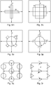
- Fig. 3a and 3b hexagonal arrays of hexagonal antenna elements are shown. According to Fig. 3a the side surfaces are parallel to each other while according to Fig. 3b each showing the corners to each other.
- 3e and 3f correspond Fig. 3b or 3a.
- FIG. 3g and 3h are shown star-shaped antenna elements, wherein Fig. 3g shows a hexagonal arrangement, with the tip of the star-shaped antenna elements facing each other. In contrast, according to Fig. 3h the sides of the star-shaped antenna elements to each other.
- Fig. 3i shows a hexagonal array of square antenna elements.
- FIGS. 3j and 3k There are combinations of a square and triangles, each with a square in the middle and triangles on the side surfaces in an orthogonal arrangement. According to Fig. 3j the square is arranged with its side surfaces parallel to the unit cell, according to Fig. 3k the square is turned 45 ° so that the peaks point to the triangles.
- Fig. 3m shows a cross structure of two crossed bars.
- Fig. 3n shows a cross structure with a large square, at the corners of each small squares are cut out.
- Fig. 3o shows a cross structure with a central circle on the smaller angular rectangles are placed on the outside at angular intervals of 90 ° to each other. According to Fig. 3o The rectangles are rotated by 45 ° and thus point to the corners of the unit cell. According to Fig. 3p show the attached rectangles parallel to the side surface of the unit cell.
- Fig. 3q shows a hexagonal arrangement of cylinders.
- Fig. 3r shows a hexagonal arrangement of equilateral triangles.
- Fig. 3s shows cylinder in orthogonal arrangement.
- Hexagonal Shape Hexagon (regular) Period (P): from 260 to 460 nm Radius (r): 62.5 nm Distance (d): 9.0 nm Material: Silver (Ag) varies: Height (h) of the structure from 36 nm to 109 nm (36, 50, 64, 70, 80, 109 nm)
- Series 5 Hexagon with a smaller radius than in series 2 side faces are parallel to each other ( Fig.
- Hexagonal Shape Hexagon (regular) Period (P): from 260 to 460 nm Radius (r): 62.5 nm Distance (d): 9.0 nm Material; Silver (Ag) varies: Height (h) of the structure from 36 nm to 100 nm (36, 50, 64, 70, 80, 100 nm) Series 6: Star (6 points), corners point to each other ( Fig.
- Hexagonal Shape Hexagon (regular) Period (P): from 265.5 to 460 nm Radius (r): 125 nm (r1), 62.5 nm (r2) Distance (d): 9 nm Material: Silver (Ag) varies: Height (h) from 36 nm to 64 nm (36, 50, 64 nm) Series 7: Star (6 points), sides pointing to each other ( Fig.
- Hexagonal Shape Hexagon (regular) Period (P): from 265.5 to 460 nm Radius (r): 125 nm (r1), 62.5 nm (r2) Distance (d): 9 nm Material: Silver (Ag) varies: Height (h) from 36 nm to 64 nm (36, 50, 64 nm) Series 8: Square side faces are parallel to each other ( Fig.
- Table 1 summarizes further simulation results in additional series 19 to 28. They refer respectively to the cylinder with orthogonal arrangement according to Fig. 3s ,
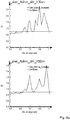
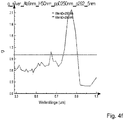
- FIGS. 4a to 4l Selected simulation results concerning the calculated absorption increases g as a function of the wavelength are given in FIGS FIGS. 4a to 4l summarized. As can be seen from the individual representations, some show strong absorption increases in preferred wavelength ranges.
- the properties of the plasmons in the antireflection layers thus not only enable improved photon management, but also, using special design parameters, an optical filter function or signal attenuation and a simultaneous amplification of specific frequency ranges can be achieved.
- the nano-antenna elements 22 can be adapted accordingly with respect to their design parameters to effect special properties in the range of optical sensors.
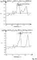
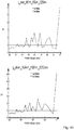
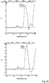
- FIG. 4a shows simulation results for the cross structure according to series 11 according to Table 1.
- the representation of the absorption increase as a function of the wavelength shows two strong peaks at about 1050 nanometers and 725 nanometers with an up to 6-fold gain.
- the remaining frequency range remains unaffected or only relatively weakly amplified up to a range of approximately 550 nanometers.
- the position of the peaks or their height can be influenced by the design parameters.
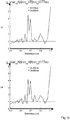
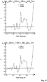
- Fig. 4b shows simulation results for the cross structure according to series 12 and 13. It can be seen that there are two strong peaks at 1050 and 825 nanometers, with up to a 16-fold gain. The remaining frequency range remains unaffected or only relatively weakly amplified. The position of the peaks or their height can be influenced by the design parameters.
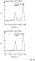
- Fig. 4c shows further simulation results for the cross structure according to series 16.
- the remaining frequency range remains unaffected or only relatively weakly amplified up to a range of approximately 550 nanometers.
- the position of the peaks or their height can be influenced by the design parameters.
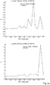
- Fig. 4d shows simulation results for the cross structure according to series 15. It can be seen that there are two very strong peaks at about 1000 nanometers and about 750 nanometers, with up to a 4-fold gain. The remaining frequency range remains unaffected or only relatively weakly amplified up to a range of approximately 550 nanometers. The position of the peaks or their height can be influenced by the design parameters.
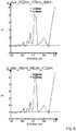
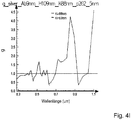
- Fig. 4e shows simulation results for the triangular structure according to series 17. It can be seen that a very strong peak occurs at about 1050 nanometers with up to a 19-fold gain. The remaining frequency range remains unaffected or only relatively weakly amplified. The position of the peaks or their height can be influenced by the design parameters.
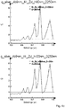
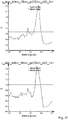
- Fig. 4f shows simulation results for the star structure according to series 6 and 7. It can be seen that a very strong peak at about 825 nanometers means a gain of up to 3.3 times. The remaining frequency range remains unaffected or only relatively weakly amplified. The position of the peaks or their height can be influenced by the design parameters.
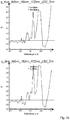
- Fig. 4g to l shows simulation results for the square structure according to series 8. There are three strong peaks at about 1100 nanometers, 850 nanometers and 725 nanometers with up to 7-fold amplification. The remaining frequency range remains unaffected or only relatively weakly amplified. The position of the peaks or their height can be influenced by the design parameters.
- the absorption properties can be specifically influenced in order to amplify certain frequency ranges, which is advantageous for use as a sensor.
- the antenna elements 22 are cylindrical in orthogonal configuration with a period of 525 nanometers.
- the radius is 125 nanometers and the height h is 70 nanometers.
- the distance d from the absorber layer 12 is 9 nanometers.
- the radius of the cylinders is 95 nanometers and the height h is 70 nanometers.
- the distance d from the absorber layer 12 is 9 nanometers.
- the period is optimally 490 nanometers.
Claims (14)
- Cellule photoélectrique, en particulier cellule solaire, comportant une couche absorbante (12) devant laquelle est disposée une couche antiréfléchissante (16), dans laquelle la couche antiréfléchissante (16) comprend une couche nanostructurée (20) comportant des éléments d'antenne (22) en matériau électriquement conducteur selon un agencement périodique, qui est disposée à une distance (d) de 1 à 50 nanomètres de la couche absorbante (12) et qui est reçue au moins partiellement dans la couche antiréfléchissante (16), dans laquelle les éléments d'antenne (22) présentent une hauteur de plus de 30 à 120 nanomètres, et dans laquelle la couche nanostructurée (20) forme en association avec un contact arrière (14) de la cellule photoélectrique (10) un résonateur optique, caractérisée en ce que les éléments d'antenne sont disposés périodiquement à des distances supérieures à 250 à 750 nanomètres les uns des autres.
- Cellule photoélectrique selon la revendication 1, caractérisée en ce que la couche nanostructurée (20) est disposée à une distance de 2 à 20 nanomètres de la couche absorbante (12), de préférence à une distance de 5 à 15 nanomètres, et de manière particulièrement préférable, de 7 à 12 nanomètres.
- Cellule photoélectrique selon l'une quelconque des revendications précédentes, caractérisée en ce que les éléments d'antenne (22) présentent une extension transversale maximale de 20 à 400 nanomètres, de préférence de 40 à 250 nanomètres, et de manière particulièrement préférable, de 100 à 250 nanomètres.
- Cellule photoélectrique selon l'une quelconque des revendications précédentes, caractérisée en ce que les éléments d'antenne (22) présentent une extension transversale minimale de 25 nanomètres, de préférence de 30 nanomètres, et de manière particulièrement préférable, de 50 nanomètres.
- Cellule photoélectrique selon l'une quelconque des revendications précédentes, dans laquelle la couche nanostructurée est constituée de SiOxNy, d'oxyde de titane ou d'ITO.
- Cellule photoélectrique selon l'une quelconque des revendications précédentes, caractérisée en ce que la couche nanostructurée (20) est constituée d'éléments d'antenne identiques ou d'éléments d'antenne de formes et/ou de tailles différentes qui sont combinés les uns aux autres selon un motif régulier.
- Cellule photoélectrique selon l'une quelconque des revendications précédentes, caractérisée en ce que la couche nanostructurée est constituée d'éléments d'antenne circulaires, polygonaux, triangulaires ou carrés (22), d'éléments d'antenne cruciformes, sous forme de barres croisées agencées de manière symétrique, sous forme d'un carré comportant de plus petits carrés agencés de manière symétrique sur chaque côté extérieur, sous forme d'un carré comportant dans chaque zone d'angle des évidements carrés agencés de manière symétrique, ou sous forme d'un cercle comportant quatre rectangles tangentiels agencés de manière symétrique, dans laquelle les rectangles sont soit disposés dans la direction d'une cellule élémentaire, soit décalés de 45° par rapport à celle-ci, soit constitués d'éléments en forme d'étoile ayant six branches qui sont disposés de manière hexagonale sur une cellule élémentaire, dans laquelle les branches des éléments d'antenne en forme d'étoile sont orientés les unes vers les autres ou les côtés situés entre les branches sont orientés les uns vers les autres.
- Cellule photoélectrique selon la revendication 7, caractérisée en ce que les éléments d'antenne (22) sont réalisés sous la forme de cylindres ou de prismes droits s'étendant perpendiculairement à une direction d'extension principale de la cellule photoélectrique (10).
- Cellule photoélectrique selon l'une quelconque des revendications précédentes, dans laquelle les éléments d'antenne sont constitués d'un métal choisi dans le groupe constitué de l'argent, du cuivre, de l'aluminium, de l'or et d'alliages de ceux-ci.
- Cellule photoélectrique selon l'une quelconque des revendications précédentes, caractérisée en ce que les éléments d'antenne sont constitués d'un métal choisi dans le groupe constitué de l'argent, du cuivre, de l'aluminium, de l'or et d'alliages de ceux-ci, et dans laquelle au moins un côté des éléments d'antenne qui est tourné vers l'absorbeur ou en sens opposé à l'absorbeur est revêtu d'un autre métal choisi dans le groupe constitué de l'argent, du cuivre, de l'aluminium, de l'or et d'alliages de ceux-ci.
- Cellule solaire selon l'une quelconque des revendications précédentes, qui est réalisée sous la forme d'une cellule solaire au silicium, dans laquelle la couche nanostructurée est de préférence constituée de cylindres droits, caractérisée en ce que la couche nanostructurée comprend des cylindres présentant un diamètre de 150 à 250 nanomètres, de préférence de 180 à 200 nanomètres, et présentant une hauteur de 50 à 90 nanomètres, qui sont disposés de préférence de manière orthogonale à une distance de 400 à 600 nanomètres, de préférence de 450 à 510 nanomètres, et qui présentent une distance de 5 à 13 nanomètres, de préférence de 8 à 10 nanomètres, par rapport à la couche absorbante.
- Cellule solaire selon la revendication 11, qui est une réalisée sous la forme d'une cellule solaire à couche épaisse standard présentant une épaisseur allant jusqu'à 200 micromètres, caractérisée en ce que les cylindres de la couche nanostructurée présentent un diamètre de 185 à 195 nanomètres, de préférence d'environ 190 nanomètres, présentent une hauteur de 68 à 72 nanomètres, de préférence d'environ 70 nanomètres, une distance par rapport à la couche absorbante de 8,5 à 9,5 nanomètres, de préférence d'environ 9 nanomètres, et sont disposés à une distance de 460 à 470 nanomètres, de préférence d'environ 465 nanomètres, selon un motif orthogonal les uns par rapport aux autres.
- Cellule solaire selon la revendication 12, qui est réalisée sous la forme d'une cellule solaire à couche épaisse HIT (10) présentant une épaisseur allant jusqu'à 200 micromètres, caractérisée en ce que les cylindres de la couche nanostructurée (20) présentent un diamètre d'environ 185 à 195 nanomètres, de préférence d'environ 190 nanomètres, présentent une hauteur (h) de 68 à 72 nanomètres, de préférence d'environ 70 nanomètres, une distance (d) par rapport à la couche absorbante (12) de 8,5 à 9,5 nanomètres, de préférence d'environ 9 nanomètres, et sont disposés à une distance de 485 à 495 nanomètres, de préférence d'environ 490 nanomètres, selon un motif orthogonal les uns par rapport aux autres.
- Cellule solaire selon l'une quelconque des revendications 1 à 10, qui est réalisée sous la forme d'une cellule solaire au silicium, en particulier sous la forme d'une cellule solaire à couches ultra-minces, caractérisée en ce que la couche nanostructurée est constituée de cylindres présentant un diamètre de 200 à 300 nanomètres, de préférence d'environ 250 nanomètres, et présentant une hauteur (h) de 50 à 90 nanomètres, de préférence d'environ 70 nanomètres, qui sont disposés selon un motif orthogonal avec un espacement de 400 à 600 nanomètres, de préférence d'environ 525 nanomètres, et présentent une distance (d) de 5 à 13 nanomètres, de préférence d'environ 9 nanomètres, par rapport à la couche absorbante (12).
Applications Claiming Priority (2)
| Application Number | Priority Date | Filing Date | Title |
|---|---|---|---|
| DE102013109143.1A DE102013109143A1 (de) | 2013-08-23 | 2013-08-23 | Photozelle, insbesondere Solarzelle sowie Verfahren zum Herstellen einer Photozelle |
| PCT/EP2014/067450 WO2015024866A1 (fr) | 2013-08-23 | 2014-08-14 | Cellule photoélectrique, en particulier cellule solaire, ainsi que procédé de fabrication d'une cellule photoélectrique |
Publications (2)
| Publication Number | Publication Date |
|---|---|
| EP3036772A1 EP3036772A1 (fr) | 2016-06-29 |
| EP3036772B1 true EP3036772B1 (fr) | 2019-06-19 |
Family
ID=51359389
Family Applications (1)
| Application Number | Title | Priority Date | Filing Date |
|---|---|---|---|
| EP14752843.4A Active EP3036772B1 (fr) | 2013-08-23 | 2014-08-14 | Cellule photoélectrique, en particulier cellule solaire, ainsi que procédé de fabrication d'une cellule photoélectrique |
Country Status (8)
| Country | Link |
|---|---|
| US (1) | US20160315206A1 (fr) |
| EP (1) | EP3036772B1 (fr) |
| JP (2) | JP2016530724A (fr) |
| KR (1) | KR20160065096A (fr) |
| CN (1) | CN105830224B (fr) |
| AU (1) | AU2014310698B2 (fr) |
| DE (1) | DE102013109143A1 (fr) |
| WO (1) | WO2015024866A1 (fr) |
Families Citing this family (3)
| Publication number | Priority date | Publication date | Assignee | Title |
|---|---|---|---|---|
| US10319868B2 (en) * | 2017-01-06 | 2019-06-11 | Nanoclear Technologies Inc. | Methods and systems to boost efficiency of solar cells |
| CN106876513B (zh) * | 2017-03-06 | 2018-08-21 | 东南大学 | 一种等离极化激元横向异质集成的太阳电池 |
| FI129724B (en) * | 2019-03-25 | 2022-07-29 | Teknologian Tutkimuskeskus Vtt Oy | Enhancing the absorption and detection of infrared radiation using plasmonics |
Family Cites Families (18)
| Publication number | Priority date | Publication date | Assignee | Title |
|---|---|---|---|---|
| JPS5791564A (en) * | 1980-11-28 | 1982-06-07 | Toshiba Corp | Solar battery |
| EP1365455A4 (fr) * | 2001-01-31 | 2006-09-20 | Shinetsu Handotai Kk | Cellule solaire et son procede de fabrication |
| FR2883663B1 (fr) * | 2005-03-22 | 2007-05-11 | Commissariat Energie Atomique | Procede de fabrication d'une cellule photovoltaique a base de silicium en couche mince. |
| US20090266415A1 (en) * | 2006-06-27 | 2009-10-29 | Liquidia Technologies , Inc. | Nanostructures and materials for photovoltaic devices |
| US8482197B2 (en) * | 2006-07-05 | 2013-07-09 | Hamamatsu Photonics K.K. | Photocathode, electron tube, field assist type photocathode, field assist type photocathode array, and field assist type electron tube |
| EP2109147A1 (fr) * | 2008-04-08 | 2009-10-14 | FOM Institute for Atomic and Molueculair Physics | Cellule photovoltaïque avec nano-structures à génération de résonance à plasmons de surface |
| US20090253227A1 (en) * | 2008-04-08 | 2009-10-08 | Defries Anthony | Engineered or structured coatings for light manipulation in solar cells and other materials |
| US20110247690A1 (en) * | 2008-12-17 | 2011-10-13 | David Thomas Crouse | Semiconductor devices comprising antireflective conductive layers and methods of making and using |
| WO2010118418A2 (fr) * | 2009-04-10 | 2010-10-14 | Lightwave Power, Inc. | Dispositif plasmonique plan pour réflexion, diffusion et guidage de lumière |
| WO2011108259A1 (fr) * | 2010-03-02 | 2011-09-09 | 国立大学法人北海道大学 | Procédé de production d'un motif de résine photosensible |
| FR2959352B1 (fr) * | 2010-04-23 | 2014-02-21 | Centre Nat Rech Scient | Structure nanometrique absorbante de type mim asymetrique et methode de realisation d'une telle structure |
| JP5649856B2 (ja) * | 2010-06-14 | 2015-01-07 | 国立大学法人 東京大学 | 光電変換素子 |
| US8338211B2 (en) * | 2010-07-27 | 2012-12-25 | Amtech Systems, Inc. | Systems and methods for charging solar cell layers |
| US8216872B1 (en) * | 2011-02-21 | 2012-07-10 | National Applied Research Laboratories | Method of integrating light-trapping layer to thin-film solar cell |
| WO2012123620A1 (fr) * | 2011-03-16 | 2012-09-20 | Aalto University Foundation | Structure de cellule photovoltaïque à couches minces, nanoantenne et procédé de fabrication |
| CN102184975A (zh) * | 2011-04-11 | 2011-09-14 | 复旦大学 | 一种能增加光电转换效率的薄膜太阳能电池及其制造方法 |
| JP5713856B2 (ja) * | 2011-09-26 | 2015-05-07 | 株式会社東芝 | 光透過型金属電極、電子装置及び光学素子 |
| CN103078057B (zh) * | 2013-01-29 | 2016-01-20 | 苏州大学 | 有机太阳能电池及其制作方法 |
-
2013
- 2013-08-23 DE DE102013109143.1A patent/DE102013109143A1/de not_active Withdrawn
-
2014
- 2014-08-14 WO PCT/EP2014/067450 patent/WO2015024866A1/fr active Application Filing
- 2014-08-14 JP JP2016535428A patent/JP2016530724A/ja active Pending
- 2014-08-14 EP EP14752843.4A patent/EP3036772B1/fr active Active
- 2014-08-14 KR KR1020167007669A patent/KR20160065096A/ko not_active Application Discontinuation
- 2014-08-14 AU AU2014310698A patent/AU2014310698B2/en active Active
- 2014-08-14 CN CN201480058264.0A patent/CN105830224B/zh active Active
-
2016
- 2016-02-23 US US15/050,795 patent/US20160315206A1/en not_active Abandoned
-
2018
- 2018-11-27 JP JP2018221235A patent/JP2019036755A/ja active Pending
Non-Patent Citations (1)
| Title |
|---|
| None * |
Also Published As
| Publication number | Publication date |
|---|---|
| CN105830224A (zh) | 2016-08-03 |
| AU2014310698B2 (en) | 2018-11-01 |
| WO2015024866A1 (fr) | 2015-02-26 |
| EP3036772A1 (fr) | 2016-06-29 |
| JP2019036755A (ja) | 2019-03-07 |
| AU2014310698A1 (en) | 2016-04-14 |
| JP2016530724A (ja) | 2016-09-29 |
| CN105830224B (zh) | 2018-07-06 |
| DE102013109143A1 (de) | 2015-02-26 |
| US20160315206A1 (en) | 2016-10-27 |
| KR20160065096A (ko) | 2016-06-08 |
Similar Documents
| Publication | Publication Date | Title |
|---|---|---|
| DE60222004T2 (de) | Transparentes substrat beschichtet mit einer elektrode | |
| DE112012002461B4 (de) | Gleichmässig verteilte selbstorganisierte kegelförmige Säulen für Solarzellen mit hohem Wirkungsgrad | |
| WO2007110392A1 (fr) | Composants optiques antireflets à large bande avec surfaces incurvées et leur procédé de fabrication | |
| DE2828744A1 (de) | Vorrichtung zum absorbieren von sonnenenergie und verfahren zur herstellung einer derartigen vorrichtung | |
| EP0664926B1 (fr) | Dispositif pour absorber des rayons infrarouges | |
| WO2008037506A1 (fr) | Nanostructures en aiguilles auto-organisées dans leurs applications | |
| DE112010002936T5 (de) | Verfahren zum Aufrauen einer Substratoberfläche, Verfahren zum Herstellen einer Fotovoltaikvorrichtung und Fotovoltaikvorrichtung | |
| EP2481092A2 (fr) | Cellule solaire | |
| EP3036772B1 (fr) | Cellule photoélectrique, en particulier cellule solaire, ainsi que procédé de fabrication d'une cellule photoélectrique | |
| DE112018004186T5 (de) | Fertigungsprozesse für effektiv transparente Kontakte | |
| DE3508469A1 (de) | Verfahren zum strukturieren von auf einem transparenten substrat aufgebrachten schichtfolgen | |
| WO1992014270A1 (fr) | Cellule solaire | |
| DE202011003479U1 (de) | Strukturierte Siliziumschicht für ein optoelektronisches Bauelement und optoelektronisches Bauelement | |
| WO2007042520A2 (fr) | Nanostructures en aiguilles auto-organisees et leur production sur du silicium | |
| WO2014023809A2 (fr) | Procédé et banc de traitement à laser pour métalliser la face arrière d'un composant à semi-conducteur | |
| DE102011112696B4 (de) | Solarzelle mit Folie zur Rückseitenkontaktierung, Verfahren zu deren Herstellung und Verwendung einer Folie als Rückseitenkontaktierung | |
| DE102012105457B3 (de) | Schichtsystem für eine transparente Elektrode und Verfahren zu dessen Herstellung | |
| EP3449509B1 (fr) | Support transparent pour structure de couches minces semi-conductrice ainsi que procédé de production et utilisation du support transparent | |
| DE102022105533B3 (de) | Verfahren zur Herstellung von Perowskit/Silizium-Tandemsolarzellen | |
| EP2443661A2 (fr) | Cellule solaire et procédé de fabrication de ladite cellule | |
| AT518236B1 (de) | Optischer Filter | |
| DE102020126116A1 (de) | Mehrfachsolarzelle und Verwendung einer Mehrfachsolarzelle | |
| DE102013113585A1 (de) | Passivierungsschicht mit Punktkontakten für Dünnschichtsolarzellen | |
| DE102013209217A1 (de) | Solarzelle mit breitbandiger Antireflexschicht, Verfahren zu deren Herstellung sowie deren Verwendung | |
| DE102011107124A1 (de) | Verfahren zur Herstellung einer Oberflächenbeschichtung mit einem Mikrostruktur-Gitter und Solarkollektor mit einer solchen Oberflächenbeschichtung |
Legal Events
| Date | Code | Title | Description |
|---|---|---|---|
| PUAI | Public reference made under article 153(3) epc to a published international application that has entered the european phase |
Free format text: ORIGINAL CODE: 0009012 |
|
| 17P | Request for examination filed |
Effective date: 20160321 |
|
| AK | Designated contracting states |
Kind code of ref document: A1 Designated state(s): AL AT BE BG CH CY CZ DE DK EE ES FI FR GB GR HR HU IE IS IT LI LT LU LV MC MK MT NL NO PL PT RO RS SE SI SK SM TR |
|
| AX | Request for extension of the european patent |
Extension state: BA ME |
|
| DAX | Request for extension of the european patent (deleted) | ||
| RAP1 | Party data changed (applicant data changed or rights of an application transferred) |
Owner name: NTS NANOTECHNOLOGYSOLAR GMBH |
|
| STAA | Information on the status of an ep patent application or granted ep patent |
Free format text: STATUS: EXAMINATION IS IN PROGRESS |
|
| 17Q | First examination report despatched |
Effective date: 20170927 |
|
| RAP1 | Party data changed (applicant data changed or rights of an application transferred) |
Owner name: F.U.N.K.E. NANOSOLAR GMBH |
|
| RIC1 | Information provided on ipc code assigned before grant |
Ipc: H01L 31/0216 20140101AFI20181122BHEP Ipc: H01L 31/056 20140101ALI20181122BHEP Ipc: H01L 31/0232 20140101ALI20181122BHEP |
|
| GRAP | Despatch of communication of intention to grant a patent |
Free format text: ORIGINAL CODE: EPIDOSNIGR1 |
|
| STAA | Information on the status of an ep patent application or granted ep patent |
Free format text: STATUS: GRANT OF PATENT IS INTENDED |
|
| INTG | Intention to grant announced |
Effective date: 20190103 |
|
| GRAS | Grant fee paid |
Free format text: ORIGINAL CODE: EPIDOSNIGR3 |
|
| GRAA | (expected) grant |
Free format text: ORIGINAL CODE: 0009210 |
|
| STAA | Information on the status of an ep patent application or granted ep patent |
Free format text: STATUS: THE PATENT HAS BEEN GRANTED |
|
| AK | Designated contracting states |
Kind code of ref document: B1 Designated state(s): AL AT BE BG CH CY CZ DE DK EE ES FI FR GB GR HR HU IE IS IT LI LT LU LV MC MK MT NL NO PL PT RO RS SE SI SK SM TR |
|
| REG | Reference to a national code |
Ref country code: GB Ref legal event code: FG4D Free format text: NOT ENGLISH |
|
| REG | Reference to a national code |
Ref country code: CH Ref legal event code: EP |
|
| REG | Reference to a national code |
Ref country code: IE Ref legal event code: FG4D Free format text: LANGUAGE OF EP DOCUMENT: GERMAN |
|
| REG | Reference to a national code |
Ref country code: DE Ref legal event code: R096 Ref document number: 502014012016 Country of ref document: DE |
|
| REG | Reference to a national code |
Ref country code: AT Ref legal event code: REF Ref document number: 1146599 Country of ref document: AT Kind code of ref document: T Effective date: 20190715 |
|
| REG | Reference to a national code |
Ref country code: NL Ref legal event code: FP |
|
| PG25 | Lapsed in a contracting state [announced via postgrant information from national office to epo] |
Ref country code: LT Free format text: LAPSE BECAUSE OF FAILURE TO SUBMIT A TRANSLATION OF THE DESCRIPTION OR TO PAY THE FEE WITHIN THE PRESCRIBED TIME-LIMIT Effective date: 20190619 Ref country code: FI Free format text: LAPSE BECAUSE OF FAILURE TO SUBMIT A TRANSLATION OF THE DESCRIPTION OR TO PAY THE FEE WITHIN THE PRESCRIBED TIME-LIMIT Effective date: 20190619 Ref country code: NO Free format text: LAPSE BECAUSE OF FAILURE TO SUBMIT A TRANSLATION OF THE DESCRIPTION OR TO PAY THE FEE WITHIN THE PRESCRIBED TIME-LIMIT Effective date: 20190919 Ref country code: AL Free format text: LAPSE BECAUSE OF FAILURE TO SUBMIT A TRANSLATION OF THE DESCRIPTION OR TO PAY THE FEE WITHIN THE PRESCRIBED TIME-LIMIT Effective date: 20190619 Ref country code: HR Free format text: LAPSE BECAUSE OF FAILURE TO SUBMIT A TRANSLATION OF THE DESCRIPTION OR TO PAY THE FEE WITHIN THE PRESCRIBED TIME-LIMIT Effective date: 20190619 Ref country code: SE Free format text: LAPSE BECAUSE OF FAILURE TO SUBMIT A TRANSLATION OF THE DESCRIPTION OR TO PAY THE FEE WITHIN THE PRESCRIBED TIME-LIMIT Effective date: 20190619 |
|
| REG | Reference to a national code |
Ref country code: LT Ref legal event code: MG4D |
|
| PG25 | Lapsed in a contracting state [announced via postgrant information from national office to epo] |
Ref country code: LV Free format text: LAPSE BECAUSE OF FAILURE TO SUBMIT A TRANSLATION OF THE DESCRIPTION OR TO PAY THE FEE WITHIN THE PRESCRIBED TIME-LIMIT Effective date: 20190619 Ref country code: GR Free format text: LAPSE BECAUSE OF FAILURE TO SUBMIT A TRANSLATION OF THE DESCRIPTION OR TO PAY THE FEE WITHIN THE PRESCRIBED TIME-LIMIT Effective date: 20190920 Ref country code: RS Free format text: LAPSE BECAUSE OF FAILURE TO SUBMIT A TRANSLATION OF THE DESCRIPTION OR TO PAY THE FEE WITHIN THE PRESCRIBED TIME-LIMIT Effective date: 20190619 Ref country code: BG Free format text: LAPSE BECAUSE OF FAILURE TO SUBMIT A TRANSLATION OF THE DESCRIPTION OR TO PAY THE FEE WITHIN THE PRESCRIBED TIME-LIMIT Effective date: 20190919 |
|
| PG25 | Lapsed in a contracting state [announced via postgrant information from national office to epo] |
Ref country code: SK Free format text: LAPSE BECAUSE OF FAILURE TO SUBMIT A TRANSLATION OF THE DESCRIPTION OR TO PAY THE FEE WITHIN THE PRESCRIBED TIME-LIMIT Effective date: 20190619 Ref country code: RO Free format text: LAPSE BECAUSE OF FAILURE TO SUBMIT A TRANSLATION OF THE DESCRIPTION OR TO PAY THE FEE WITHIN THE PRESCRIBED TIME-LIMIT Effective date: 20190619 Ref country code: CZ Free format text: LAPSE BECAUSE OF FAILURE TO SUBMIT A TRANSLATION OF THE DESCRIPTION OR TO PAY THE FEE WITHIN THE PRESCRIBED TIME-LIMIT Effective date: 20190619 Ref country code: PT Free format text: LAPSE BECAUSE OF FAILURE TO SUBMIT A TRANSLATION OF THE DESCRIPTION OR TO PAY THE FEE WITHIN THE PRESCRIBED TIME-LIMIT Effective date: 20191021 Ref country code: EE Free format text: LAPSE BECAUSE OF FAILURE TO SUBMIT A TRANSLATION OF THE DESCRIPTION OR TO PAY THE FEE WITHIN THE PRESCRIBED TIME-LIMIT Effective date: 20190619 |
|
| PG25 | Lapsed in a contracting state [announced via postgrant information from national office to epo] |
Ref country code: ES Free format text: LAPSE BECAUSE OF FAILURE TO SUBMIT A TRANSLATION OF THE DESCRIPTION OR TO PAY THE FEE WITHIN THE PRESCRIBED TIME-LIMIT Effective date: 20190619 Ref country code: IT Free format text: LAPSE BECAUSE OF FAILURE TO SUBMIT A TRANSLATION OF THE DESCRIPTION OR TO PAY THE FEE WITHIN THE PRESCRIBED TIME-LIMIT Effective date: 20190619 Ref country code: SM Free format text: LAPSE BECAUSE OF FAILURE TO SUBMIT A TRANSLATION OF THE DESCRIPTION OR TO PAY THE FEE WITHIN THE PRESCRIBED TIME-LIMIT Effective date: 20190619 Ref country code: IS Free format text: LAPSE BECAUSE OF FAILURE TO SUBMIT A TRANSLATION OF THE DESCRIPTION OR TO PAY THE FEE WITHIN THE PRESCRIBED TIME-LIMIT Effective date: 20191019 |
|
| PG25 | Lapsed in a contracting state [announced via postgrant information from national office to epo] |
Ref country code: TR Free format text: LAPSE BECAUSE OF FAILURE TO SUBMIT A TRANSLATION OF THE DESCRIPTION OR TO PAY THE FEE WITHIN THE PRESCRIBED TIME-LIMIT Effective date: 20190619 |
|
| PG25 | Lapsed in a contracting state [announced via postgrant information from national office to epo] |
Ref country code: PL Free format text: LAPSE BECAUSE OF FAILURE TO SUBMIT A TRANSLATION OF THE DESCRIPTION OR TO PAY THE FEE WITHIN THE PRESCRIBED TIME-LIMIT Effective date: 20190619 Ref country code: DK Free format text: LAPSE BECAUSE OF FAILURE TO SUBMIT A TRANSLATION OF THE DESCRIPTION OR TO PAY THE FEE WITHIN THE PRESCRIBED TIME-LIMIT Effective date: 20190619 |
|
| PG25 | Lapsed in a contracting state [announced via postgrant information from national office to epo] |
Ref country code: LU Free format text: LAPSE BECAUSE OF NON-PAYMENT OF DUE FEES Effective date: 20190814 Ref country code: MC Free format text: LAPSE BECAUSE OF FAILURE TO SUBMIT A TRANSLATION OF THE DESCRIPTION OR TO PAY THE FEE WITHIN THE PRESCRIBED TIME-LIMIT Effective date: 20190619 Ref country code: IS Free format text: LAPSE BECAUSE OF FAILURE TO SUBMIT A TRANSLATION OF THE DESCRIPTION OR TO PAY THE FEE WITHIN THE PRESCRIBED TIME-LIMIT Effective date: 20200224 |
|
| REG | Reference to a national code |
Ref country code: BE Ref legal event code: MM Effective date: 20190831 |
|
| REG | Reference to a national code |
Ref country code: DE Ref legal event code: R097 Ref document number: 502014012016 Country of ref document: DE |
|
| PLBE | No opposition filed within time limit |
Free format text: ORIGINAL CODE: 0009261 |
|
| STAA | Information on the status of an ep patent application or granted ep patent |
Free format text: STATUS: NO OPPOSITION FILED WITHIN TIME LIMIT |
|
| PG2D | Information on lapse in contracting state deleted |
Ref country code: IS |
|
| PG25 | Lapsed in a contracting state [announced via postgrant information from national office to epo] |
Ref country code: IE Free format text: LAPSE BECAUSE OF NON-PAYMENT OF DUE FEES Effective date: 20190814 |
|
| 26N | No opposition filed |
Effective date: 20200603 |
|
| PG25 | Lapsed in a contracting state [announced via postgrant information from national office to epo] |
Ref country code: SI Free format text: LAPSE BECAUSE OF FAILURE TO SUBMIT A TRANSLATION OF THE DESCRIPTION OR TO PAY THE FEE WITHIN THE PRESCRIBED TIME-LIMIT Effective date: 20190619 Ref country code: BE Free format text: LAPSE BECAUSE OF NON-PAYMENT OF DUE FEES Effective date: 20190831 |
|
| REG | Reference to a national code |
Ref country code: AT Ref legal event code: MM01 Ref document number: 1146599 Country of ref document: AT Kind code of ref document: T Effective date: 20190814 |
|
| PG25 | Lapsed in a contracting state [announced via postgrant information from national office to epo] |
Ref country code: AT Free format text: LAPSE BECAUSE OF NON-PAYMENT OF DUE FEES Effective date: 20190814 |
|
| PG25 | Lapsed in a contracting state [announced via postgrant information from national office to epo] |
Ref country code: CY Free format text: LAPSE BECAUSE OF FAILURE TO SUBMIT A TRANSLATION OF THE DESCRIPTION OR TO PAY THE FEE WITHIN THE PRESCRIBED TIME-LIMIT Effective date: 20190619 |
|
| PG25 | Lapsed in a contracting state [announced via postgrant information from national office to epo] |
Ref country code: MT Free format text: LAPSE BECAUSE OF FAILURE TO SUBMIT A TRANSLATION OF THE DESCRIPTION OR TO PAY THE FEE WITHIN THE PRESCRIBED TIME-LIMIT Effective date: 20190619 Ref country code: HU Free format text: LAPSE BECAUSE OF FAILURE TO SUBMIT A TRANSLATION OF THE DESCRIPTION OR TO PAY THE FEE WITHIN THE PRESCRIBED TIME-LIMIT; INVALID AB INITIO Effective date: 20140814 |
|
| PG25 | Lapsed in a contracting state [announced via postgrant information from national office to epo] |
Ref country code: MK Free format text: LAPSE BECAUSE OF FAILURE TO SUBMIT A TRANSLATION OF THE DESCRIPTION OR TO PAY THE FEE WITHIN THE PRESCRIBED TIME-LIMIT Effective date: 20190619 |
|
| P01 | Opt-out of the competence of the unified patent court (upc) registered |
Effective date: 20230508 |
|
| PGFP | Annual fee paid to national office [announced via postgrant information from national office to epo] |
Ref country code: NL Payment date: 20230821 Year of fee payment: 10 |
|
| PGFP | Annual fee paid to national office [announced via postgrant information from national office to epo] |
Ref country code: GB Payment date: 20230822 Year of fee payment: 10 Ref country code: CH Payment date: 20230902 Year of fee payment: 10 |
|
| PGFP | Annual fee paid to national office [announced via postgrant information from national office to epo] |
Ref country code: FR Payment date: 20230825 Year of fee payment: 10 Ref country code: DE Payment date: 20230926 Year of fee payment: 10 |