EP3036772B1 - Photocell, in particular solar cell and method for producing a photocell - Google Patents
Photocell, in particular solar cell and method for producing a photocell Download PDFInfo
- Publication number
- EP3036772B1 EP3036772B1 EP14752843.4A EP14752843A EP3036772B1 EP 3036772 B1 EP3036772 B1 EP 3036772B1 EP 14752843 A EP14752843 A EP 14752843A EP 3036772 B1 EP3036772 B1 EP 3036772B1
- Authority
- EP
- European Patent Office
- Prior art keywords
- nanometers
- layer
- antenna elements
- distance
- solar cell
- Prior art date
- Legal status (The legal status is an assumption and is not a legal conclusion. Google has not performed a legal analysis and makes no representation as to the accuracy of the status listed.)
- Active
Links
- 238000004519 manufacturing process Methods 0.000 title description 13
- BQCADISMDOOEFD-UHFFFAOYSA-N Silver Chemical compound [Ag] BQCADISMDOOEFD-UHFFFAOYSA-N 0.000 claims description 46
- 229910052709 silver Inorganic materials 0.000 claims description 45
- 239000004332 silver Substances 0.000 claims description 45
- 239000000463 material Substances 0.000 claims description 41
- 239000006096 absorbing agent Substances 0.000 claims description 30
- XUIMIQQOPSSXEZ-UHFFFAOYSA-N Silicon Chemical compound [Si] XUIMIQQOPSSXEZ-UHFFFAOYSA-N 0.000 claims description 12
- PCHJSUWPFVWCPO-UHFFFAOYSA-N gold Chemical compound [Au] PCHJSUWPFVWCPO-UHFFFAOYSA-N 0.000 claims description 12
- 229910052737 gold Inorganic materials 0.000 claims description 12
- 239000010931 gold Substances 0.000 claims description 12
- 229910052710 silicon Inorganic materials 0.000 claims description 12
- 239000010703 silicon Substances 0.000 claims description 12
- 229910052751 metal Inorganic materials 0.000 claims description 11
- 239000002184 metal Substances 0.000 claims description 11
- 230000003287 optical effect Effects 0.000 claims description 11
- RYGMFSIKBFXOCR-UHFFFAOYSA-N Copper Chemical compound [Cu] RYGMFSIKBFXOCR-UHFFFAOYSA-N 0.000 claims description 10
- 229910052802 copper Inorganic materials 0.000 claims description 10
- 239000010949 copper Substances 0.000 claims description 10
- 229910045601 alloy Inorganic materials 0.000 claims description 7
- 239000000956 alloy Substances 0.000 claims description 7
- 229910052782 aluminium Inorganic materials 0.000 claims description 7
- XAGFODPZIPBFFR-UHFFFAOYSA-N aluminium Chemical compound [Al] XAGFODPZIPBFFR-UHFFFAOYSA-N 0.000 claims description 7
- 239000004020 conductor Substances 0.000 claims description 6
- 229910020286 SiOxNy Inorganic materials 0.000 claims description 2
- 239000010410 layer Substances 0.000 description 134
- 238000010521 absorption reaction Methods 0.000 description 23
- 229920002120 photoresistant polymer Polymers 0.000 description 20
- 238000000034 method Methods 0.000 description 15
- VYPSYNLAJGMNEJ-UHFFFAOYSA-N Silicium dioxide Chemical compound O=[Si]=O VYPSYNLAJGMNEJ-UHFFFAOYSA-N 0.000 description 13
- 230000006872 improvement Effects 0.000 description 13
- 238000004088 simulation Methods 0.000 description 13
- 239000010408 film Substances 0.000 description 12
- 239000011241 protective layer Substances 0.000 description 12
- 239000011248 coating agent Substances 0.000 description 8
- 238000000576 coating method Methods 0.000 description 8
- 239000002105 nanoparticle Substances 0.000 description 8
- 230000008569 process Effects 0.000 description 8
- 239000000758 substrate Substances 0.000 description 8
- 229910052581 Si3N4 Inorganic materials 0.000 description 6
- 239000002245 particle Substances 0.000 description 6
- 239000000377 silicon dioxide Substances 0.000 description 6
- 238000005530 etching Methods 0.000 description 5
- 235000012239 silicon dioxide Nutrition 0.000 description 5
- 230000000694 effects Effects 0.000 description 4
- HQVNEWCFYHHQES-UHFFFAOYSA-N silicon nitride Chemical compound N12[Si]34N5[Si]62N3[Si]51N64 HQVNEWCFYHHQES-UHFFFAOYSA-N 0.000 description 4
- 230000003321 amplification Effects 0.000 description 3
- 238000013459 approach Methods 0.000 description 3
- 230000008901 benefit Effects 0.000 description 3
- 230000008878 coupling Effects 0.000 description 3
- 238000010168 coupling process Methods 0.000 description 3
- 238000005859 coupling reaction Methods 0.000 description 3
- 238000001459 lithography Methods 0.000 description 3
- 238000003199 nucleic acid amplification method Methods 0.000 description 3
- 230000005855 radiation Effects 0.000 description 3
- 238000001228 spectrum Methods 0.000 description 3
- 239000010409 thin film Substances 0.000 description 3
- IJGRMHOSHXDMSA-UHFFFAOYSA-N Atomic nitrogen Chemical compound N#N IJGRMHOSHXDMSA-UHFFFAOYSA-N 0.000 description 2
- FOIXSVOLVBLSDH-UHFFFAOYSA-N Silver ion Chemical compound [Ag+] FOIXSVOLVBLSDH-UHFFFAOYSA-N 0.000 description 2
- 230000003667 anti-reflective effect Effects 0.000 description 2
- 238000003491 array Methods 0.000 description 2
- 238000000151 deposition Methods 0.000 description 2
- 238000009826 distribution Methods 0.000 description 2
- 238000000025 interference lithography Methods 0.000 description 2
- 238000001127 nanoimprint lithography Methods 0.000 description 2
- 239000004065 semiconductor Substances 0.000 description 2
- 229910001218 Gallium arsenide Inorganic materials 0.000 description 1
- 229910004298 SiO 2 Inorganic materials 0.000 description 1
- GWEVSGVZZGPLCZ-UHFFFAOYSA-N Titan oxide Chemical compound O=[Ti]=O GWEVSGVZZGPLCZ-UHFFFAOYSA-N 0.000 description 1
- 229910021417 amorphous silicon Inorganic materials 0.000 description 1
- 238000000137 annealing Methods 0.000 description 1
- 230000015572 biosynthetic process Effects 0.000 description 1
- 229910021419 crystalline silicon Inorganic materials 0.000 description 1
- 230000008021 deposition Effects 0.000 description 1
- 239000003989 dielectric material Substances 0.000 description 1
- 238000001312 dry etching Methods 0.000 description 1
- 238000004049 embossing Methods 0.000 description 1
- 238000001704 evaporation Methods 0.000 description 1
- 230000008020 evaporation Effects 0.000 description 1
- 230000005284 excitation Effects 0.000 description 1
- 238000001914 filtration Methods 0.000 description 1
- RHZWSUVWRRXEJF-UHFFFAOYSA-N indium tin Chemical compound [In].[Sn] RHZWSUVWRRXEJF-UHFFFAOYSA-N 0.000 description 1
- 230000001788 irregular Effects 0.000 description 1
- 238000002955 isolation Methods 0.000 description 1
- 238000011031 large-scale manufacturing process Methods 0.000 description 1
- 230000031700 light absorption Effects 0.000 description 1
- 150000002739 metals Chemical class 0.000 description 1
- 229910021421 monocrystalline silicon Inorganic materials 0.000 description 1
- 238000005329 nanolithography Methods 0.000 description 1
- 239000002086 nanomaterial Substances 0.000 description 1
- 229910052757 nitrogen Inorganic materials 0.000 description 1
- 230000010355 oscillation Effects 0.000 description 1
- TWNQGVIAIRXVLR-UHFFFAOYSA-N oxo(oxoalumanyloxy)alumane Chemical compound O=[Al]O[Al]=O TWNQGVIAIRXVLR-UHFFFAOYSA-N 0.000 description 1
- 238000000059 patterning Methods 0.000 description 1
- 238000002360 preparation method Methods 0.000 description 1
- 229910052814 silicon oxide Inorganic materials 0.000 description 1
- 238000002174 soft lithography Methods 0.000 description 1
- 230000003595 spectral effect Effects 0.000 description 1
- 238000004528 spin coating Methods 0.000 description 1
- 238000002198 surface plasmon resonance spectroscopy Methods 0.000 description 1
- 238000002207 thermal evaporation Methods 0.000 description 1
- 229910001887 tin oxide Inorganic materials 0.000 description 1
- OGIDPMRJRNCKJF-UHFFFAOYSA-N titanium oxide Inorganic materials [Ti]=O OGIDPMRJRNCKJF-UHFFFAOYSA-N 0.000 description 1
- 238000009281 ultraviolet germicidal irradiation Methods 0.000 description 1
- 238000007740 vapor deposition Methods 0.000 description 1
Images


Classifications
-
- H—ELECTRICITY
- H01—ELECTRIC ELEMENTS
- H01L—SEMICONDUCTOR DEVICES NOT COVERED BY CLASS H10
- H01L31/00—Semiconductor devices sensitive to infrared radiation, light, electromagnetic radiation of shorter wavelength or corpuscular radiation and specially adapted either for the conversion of the energy of such radiation into electrical energy or for the control of electrical energy by such radiation; Processes or apparatus specially adapted for the manufacture or treatment thereof or of parts thereof; Details thereof
- H01L31/04—Semiconductor devices sensitive to infrared radiation, light, electromagnetic radiation of shorter wavelength or corpuscular radiation and specially adapted either for the conversion of the energy of such radiation into electrical energy or for the control of electrical energy by such radiation; Processes or apparatus specially adapted for the manufacture or treatment thereof or of parts thereof; Details thereof adapted as photovoltaic [PV] conversion devices
-
- H—ELECTRICITY
- H01—ELECTRIC ELEMENTS
- H01L—SEMICONDUCTOR DEVICES NOT COVERED BY CLASS H10
- H01L31/00—Semiconductor devices sensitive to infrared radiation, light, electromagnetic radiation of shorter wavelength or corpuscular radiation and specially adapted either for the conversion of the energy of such radiation into electrical energy or for the control of electrical energy by such radiation; Processes or apparatus specially adapted for the manufacture or treatment thereof or of parts thereof; Details thereof
- H01L31/02—Details
- H01L31/0216—Coatings
- H01L31/02161—Coatings for devices characterised by at least one potential jump barrier or surface barrier
- H01L31/02167—Coatings for devices characterised by at least one potential jump barrier or surface barrier for solar cells
- H01L31/02168—Coatings for devices characterised by at least one potential jump barrier or surface barrier for solar cells the coatings being antireflective or having enhancing optical properties for the solar cells
-
- H—ELECTRICITY
- H01—ELECTRIC ELEMENTS
- H01L—SEMICONDUCTOR DEVICES NOT COVERED BY CLASS H10
- H01L31/00—Semiconductor devices sensitive to infrared radiation, light, electromagnetic radiation of shorter wavelength or corpuscular radiation and specially adapted either for the conversion of the energy of such radiation into electrical energy or for the control of electrical energy by such radiation; Processes or apparatus specially adapted for the manufacture or treatment thereof or of parts thereof; Details thereof
- H01L31/02—Details
- H01L31/0224—Electrodes
- H01L31/022466—Electrodes made of transparent conductive layers, e.g. TCO, ITO layers
- H01L31/022475—Electrodes made of transparent conductive layers, e.g. TCO, ITO layers composed of indium tin oxide [ITO]
-
- H—ELECTRICITY
- H01—ELECTRIC ELEMENTS
- H01L—SEMICONDUCTOR DEVICES NOT COVERED BY CLASS H10
- H01L31/00—Semiconductor devices sensitive to infrared radiation, light, electromagnetic radiation of shorter wavelength or corpuscular radiation and specially adapted either for the conversion of the energy of such radiation into electrical energy or for the control of electrical energy by such radiation; Processes or apparatus specially adapted for the manufacture or treatment thereof or of parts thereof; Details thereof
- H01L31/02—Details
- H01L31/0232—Optical elements or arrangements associated with the device
- H01L31/02327—Optical elements or arrangements associated with the device the optical elements being integrated or being directly associated to the device, e.g. back reflectors
-
- H—ELECTRICITY
- H01—ELECTRIC ELEMENTS
- H01L—SEMICONDUCTOR DEVICES NOT COVERED BY CLASS H10
- H01L31/00—Semiconductor devices sensitive to infrared radiation, light, electromagnetic radiation of shorter wavelength or corpuscular radiation and specially adapted either for the conversion of the energy of such radiation into electrical energy or for the control of electrical energy by such radiation; Processes or apparatus specially adapted for the manufacture or treatment thereof or of parts thereof; Details thereof
- H01L31/04—Semiconductor devices sensitive to infrared radiation, light, electromagnetic radiation of shorter wavelength or corpuscular radiation and specially adapted either for the conversion of the energy of such radiation into electrical energy or for the control of electrical energy by such radiation; Processes or apparatus specially adapted for the manufacture or treatment thereof or of parts thereof; Details thereof adapted as photovoltaic [PV] conversion devices
- H01L31/054—Optical elements directly associated or integrated with the PV cell, e.g. light-reflecting means or light-concentrating means
- H01L31/056—Optical elements directly associated or integrated with the PV cell, e.g. light-reflecting means or light-concentrating means the light-reflecting means being of the back surface reflector [BSR] type
-
- H—ELECTRICITY
- H01—ELECTRIC ELEMENTS
- H01L—SEMICONDUCTOR DEVICES NOT COVERED BY CLASS H10
- H01L31/00—Semiconductor devices sensitive to infrared radiation, light, electromagnetic radiation of shorter wavelength or corpuscular radiation and specially adapted either for the conversion of the energy of such radiation into electrical energy or for the control of electrical energy by such radiation; Processes or apparatus specially adapted for the manufacture or treatment thereof or of parts thereof; Details thereof
- H01L31/18—Processes or apparatus specially adapted for the manufacture or treatment of these devices or of parts thereof
-
- Y—GENERAL TAGGING OF NEW TECHNOLOGICAL DEVELOPMENTS; GENERAL TAGGING OF CROSS-SECTIONAL TECHNOLOGIES SPANNING OVER SEVERAL SECTIONS OF THE IPC; TECHNICAL SUBJECTS COVERED BY FORMER USPC CROSS-REFERENCE ART COLLECTIONS [XRACs] AND DIGESTS
- Y02—TECHNOLOGIES OR APPLICATIONS FOR MITIGATION OR ADAPTATION AGAINST CLIMATE CHANGE
- Y02E—REDUCTION OF GREENHOUSE GAS [GHG] EMISSIONS, RELATED TO ENERGY GENERATION, TRANSMISSION OR DISTRIBUTION
- Y02E10/00—Energy generation through renewable energy sources
- Y02E10/50—Photovoltaic [PV] energy
- Y02E10/52—PV systems with concentrators
Definitions
- the invention relates to a photocell, in particular a solar cell, with an absorber layer, is arranged in front of one of the antireflection layer.
- an antireflection layer (AR layer) is used by default, which is geometrically structured, in the form of a pyramidal structure or an inverted pyramidal structure. This achieves a significant improvement in the photon management of solar cells, thereby improving the efficiency by about 10% (relative), i. a solar cell with e.g. 20% efficiency can be increased to 22% efficiency by using an AR layer with pyramidal structure.
- the AR layer is usually made of silicon nitride and is formed as a regular pyramidal structure, wherein the base of the square pyramids is usually 2 to 10 microns long.
- the apex angle of the pyramids with a square base is about 70 °.
- a disadvantage of such AR layers is in particular that the structure works optimally only in a very narrow wavelength range of the solar spectrum.
- a first approach for improving solar cells by plasmonic structures was therefore to additionally apply nanoparticles to the surface of a conventional silicon solar cell, which is done by depositing a thin metal layer and annealing under nitrogen, so that the structure is transformed into discrete islands.
- the resulting structures were irregular.
- colloidal silver and gold nanoparticles were used as the source of scattering elements. This resulted in a uniform size and uniform density distribution of particles on the surface. This type of deposition has been used on crystalline silicon, amorphous silicon and InP / InGaAsP cells. In some cases, an improvement in efficiency of 8% was observed for silver nanoparticles.
- AAO masks anodic aluminum oxide
- evaporation masks as a means of controlling the height and density of the deposited nanoparticles.
- the highest increases in efficiency were observed in dense, high particle arrangements, which was attributed to near-field coupling between the particles.
- nanostructured AR layer of silver on the surface of silicon was also investigated.
- the nanostructured scattering objects were fins 100 nanometers wide and 50 nanometers high, starting from the back of the cell into the semiconductor. Both 6 micron and 300 nanometer distances were investigated, and certain absorption improvements were observed.
- plasmonic solar cell structures are contemplated in which resonant plasmon excitation has been made on thin-film solar cells utilizing the strong near-field enhancement around the metallic nanoparticles to improve absorption in a surrounding semiconductor material.
- the nanoparticles then act as an antenna for the incident sunlight, which is stored in a localized surface plasmon mode. This should work well especially for small particle diameters of 5 to 20 nanometers.
- the photovoltaic cell has a substrate, a first dielectric layer on the substrate, an active layer on the first dielectric layer, and a plasmonic light concentrator arrangement on the active layer to couple incident light of a first wavelength range into the active layer.
- the photovoltaic cell further comprises a second dielectric layer, which is transparent to the first wavelength range and at a second wavelength range on the plasmonic Lichtkonzentratoran ever.
- the first dielectric layer, the active layer, the plasmonic light concentrator arrangement and the second dielectric layer are configured to form a resonant cavity for coupling incident light at the second wavelength range into a wave standing in the resonant cavity.
- the invention has for its object to provide an improved photocell, in particular solar cell, with which a significant improvement in the photon management can be achieved.
- the use of a nanostructured layer with periodically arranged antenna elements of an electrically conductive material, which is arranged at a distance of 1 to 50 nanometers from the absorber layer, wherein the antenna elements are arranged with a distance of more than 250 to 750 nanometers to each other and have a height of more than 30 to 120 nanometers, achieved a significant improvement in photon management, ie Overall, a significant improvement in the absorption in the solar cell.
- the antenna elements can easily couple the entire spectrum of sunlight (from 280 nm to 1100 nm wavelength) into the solar cell and hold the light longer in the solar cell than the previously used microstructures since the nano-antenna elements resume the absorbed light in the solar cell ( received) and radiate back into the solar cell.
- the novel nanostructured layer the light can be better absorbed by a factor of 2 than with conventional AR layers in pyramidal form (the efficiency can be improved by about 20% (relative)).
- these act as surface plasmons with defined near-field properties.
- the nanostructured layer forms an optical resonator together with a back contact of the photocell.
- the plasmon structures with nanostructured layers known hitherto in the prior art either have no periodically arranged antenna elements or are still so indeterminate that no optimized properties can be achieved over a wide range.
- a particular advantage of the photocell according to the invention is that the nanostructured layer can be used with periodically arranged antenna elements in all types of photocells regardless of the structure of the photocell itself.
- the light is collected over a larger angular range and irradiated into the substrate, since the plasmons act as antennas. Also, blurring upon irradiation with infrared light is reduced by patterning. Namely, the modes are also formed in regions of the sensor layer, whereby an improved collection of the generated electrons is possible.
- the nanostructured layer is arranged at a distance of 2 to 20 nanometers from the absorber layer, preferably at a distance of 5 to 15 nanometers, particularly preferably at a distance of 7 to 12 nanometers.
- Individual antenna elements are preferably arranged periodically either orthogonal or hexagonal to one another.
- the maximum extension of the antenna elements in the transverse direction is preferably 20 to 400 nanometers, more preferably 40 to 250 nanometers, particularly preferably 100 to 250 nanometers.
- the minimum extension of the antenna elements in the transverse direction is preferably 25 nanometers, more preferably 30 nanometers, particularly preferably at least 50 nanometers.
- the nanostructured layer with the antenna elements is preferably at least partially accommodated in the antireflection layer, which preferably consists of SiOxNy (for example SiO3N4), titanium oxide or ITO ("indium tin oxide").
- the nanostructured layer partially protrudes from the antireflection coating as a result of its height, it preferably lies in a protective layer applied over it, which may be made of silicon oxide, for example.
- the nanostructured layer can consist of identical antenna elements or of antenna elements of different shape and / or size, which are combined with each other in a regular pattern.
- the nanostructured layer consists of circular, polygonal, triangular or square antenna elements, of cross-shaped antenna elements, in the form of crossed bars in a symmetrical configuration, in the form of a square with smaller squares on each outer side in a symmetrical configuration, in Shape of a square with square recesses in each corner region in a symmetrical configuration, or in the form of a circle with four tangentially patched rectangles in a symmetrical configuration, the rectangles are either arranged in the direction of a unit cell or offset by 45 ° thereto, or consists of star-shaped elements six peaks arranged hexagonally on a unit cell, with the tips of the star-shaped antenna elements facing each other or the sides between the peaks facing each other.
- antenna elements depending on the particular application, ie in particular an absorption improvement in a particular solar cell, or a targeted amplification of a particular frequency range, or filtering a certain frequency range in an application as a sensor reach.
- the antenna elements are formed as cylinders or as straight prisms, which extend perpendicular to a main extension direction of the photocell.
- the antenna elements are made of a metal selected from the group consisting of silver, copper, aluminum, gold and their alloys.
- silver is particularly preferred, but other metals may be advantageous for individual applications.
- the antenna elements are made of a metal selected from the group consisting of silver, copper, aluminum, gold and their alloys, and at least one side of the antenna elements facing the absorber or the absorber facing away from one another Metal selected from the group consisting of silver, copper, aluminum, gold and their alloys.
- the nanostructured layer consists of straight cylinders. This is particularly advantageous when the photocell is designed as a solar cell, in particular as a silicon solar cell.
- the nanostructured layer consists of cylinders with a diameter of 150 to 250 nanometers, preferably from 180 to 200 nanometers, and with a height of 50 to 90 nanometers, which are preferably arranged in an orthogonal pattern with a spacing of 400 to 600 nanometers, preferably 450 to 510 nanometers and a distance to the absorber layer of 5 to 13 nanometers, preferably from 8 to 10 nanometers.
- the solar cell is designed as a standard thick-film solar cell with a thickness of up to 200 micrometers, wherein the cylinders of the nanostructured layer have a diameter of 185 to 195 nanometers, preferably about 190 nanometers, a height of 68 to 72 nanometers, preferably about 70 nanometers, have a distance to the absorber layer of 8.5 to 9.5 nanometers, preferably about 9 nanometers, and arranged at a distance of 460 to 470 nanometers, preferably about 465 nanometers, in an orthogonal pattern to each other are.
- the solar cell is designed as a HIT thick-film solar cell with a thickness of up to 200 micrometers, wherein the cylinders of the nanostructured layer have a diameter of about 185 to 195 nanometers, preferably about 190 nanometers, a height of 68 to 72 nanometers, preferably about 70 nanometers, have a distance to the absorber layer of 8.5 to 9.5 nanometers, preferably about 9 nanometers and arranged at a distance of 485 to 495 nanometers, preferably about 490 nanometers, in an orthogonal pattern to each other are.
- the nanostructured layer advantageously consists of cylinders with a diameter of 200 to 300 nanometers, preferably about 250 nanometers, with a height of 50 to 90 nanometers, preferably about 70 nanometers, preferably in an orthogonal pattern with a spacing of 400 to 600 nanometers, preferably about 525 nanometers are arranged and have a distance to the absorber layer of 5 to 13 nanometers, preferably of about 9 nanometers.
- the ultrathin-film solar cell can be, for example, a cell approximately in the order of up to about 1000 nanometers in thickness, for example with a back contact layer of silver and a thickness of 200 nanometers, an absorber layer of silicon with a thickness of approximately 150 nanometers,
- an AR layer may be about 45 nanometers thick silicon nitride and about 64 nanometers thick silicon dioxide protective layer.
- the photocell is used as a solar cell with an absorption increase of selected frequency ranges of incident radiation.
- the photocell is used as a sensor, with an absorption increase of selected frequency ranges and / or an optical signal attenuation over a certain frequency range.
- the properties can be varied within wide limits, in order to obtain certain absorption increases of selected frequency ranges, ie to effect, for example, particular gains in individual frequency ranges.
- optical signal attenuation over a certain frequency range ie optical filter functions, can be achieved.
- a photocell according to the invention can advantageously be produced by producing the photocell with an absorber and an antireflection layer (unstructured) arranged above it, the antireflection layer having a nanostructured layer with periodically arranged antenna elements made of an electrically conductive material with a spacing of 1 to 50 nanometers is made to the absorber surface.
- At least the shape, size, arrangement, periodicity and spacing of the antenna elements are adapted to the absorber surface as a function of the design and the design parameters of the photocell to a targeted increase in absorption in a desired first frequency range and / or optical signal attenuation over a second frequency range guarantee.
- the properties of the nanostructured layer can be tailor-made with regard to the desired application.
- a production of the nanostructured layer is carried out by basically known methods, which are adapted with regard to the desired application.
- UV nano imprint lithography This involves the production of the nanostructured layer by a nanoimprint process, namely the so-called nanoprint lithography.
- a soft die is used at room temperature.
- the contact force is less than 1000 Newton.
- UV light with a wavelength range of 350 to 450 nanometers is used. It can achieve resolutions of ⁇ 15 nanometers and process substrates from 10 to 200 mm. It is the so-called UV nano imprint lithography (UV-NIL).
- the so-called nano-interference lithography can be used to produce the structuring of the photoresist layer.
- the nanostructured layer is advantageously produced on already finished solar cells, in which only the antireflection layer was produced unstructured, ie as a continuous layer without pyramidal structure.
- the nanostructured layer can thus be subsequently produced and then re-sealed again by applying a protective layer, which preferably consists of silicon dioxide.
- the production of the nanostructured layer can be easily adapted to existing manufacturing processes.
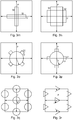
- Fig. 1 is a photocell, which is designed here as a solar cell, generally designated by the numeral 10.
- solar cell which are, for example, a standard thick-film solar cell made of (monocrystalline) silicon with an absorber layer 12, a back contact layer 14 made of silver, a front antireflection layer 16 made of silicon nitride (Si 3 N 4 ) and above a protective layer of silicon dioxide.
- a nanostructured layer 20 having antenna elements 22 is partially received in the AR layer 16 and protrudes partially into the protective layer 18.
- the nanostructured layer 20 has a height h and a distance d from the absorber layer 12.
- the individual antenna elements may consist of silver, but also of another material, such as copper, aluminum, gold or alloys thereof and may optionally be coated on the side of the AR layer 16 or on the opposite side with another material, ie eg made of silver and be coated on the AR side with gold.
- the shape, size, arrangement and other parameters of the antenna elements 22 can be varied within wide limits to produce tailored properties of the nanostructured layer with respect to the particular application.
- the antenna elements 22 together with the back contact 14 form an optical resonator, the antenna elements 22 acting as plasmons.
- simulation results are in the FIGS. 4a to 4e exemplified, will be discussed later.
- the nanostructured layer 20 is produced by methods known in the art which are adapted to the respective procedure.
- the photocell or solar cell is completely manufactured according to the method known in the art and only then applied the nanostructured layer.
- Only the antireflection layer (AR layer) 16 is produced as a flat layer and is not patterned as a pyramid pattern as is usual in the prior art.
- the advantage of subsequently producing the nanostructured layer 20 is that the photocell can be completely manufactured by known methods, so that no process changes are required.
- the solar cell is produced as known in the prior art, but with a planar AR layer 16.
- a photoresist layer is then applied to the protective layer 18, for example by spin coating.
- the substrate 24 is the protective layer 18 of the solar cell 10 (it would also be conceivable to begin immediately after the application of the AR layer 16 before the application of the protective layer 18).
- the photoresist layer 26 is then patterned by means of a stamp 28 having the pattern of the nanostructured layer 20.
- the soft, rubber stamp 28 is according to Fig.
- the nanostructured layer 20 with the discrete antenna elements 22 in the desired arrangement with the desired distance to the absorber layer 12.
- the nanostructured layer can be produced with the desired design parameters. Depending on the height of the individual antenna elements 22, they either project upwards from the AR layer 16 or are completely accommodated therein.
- the final step is then the application of a protective layer on the surface, usually silica.
- the invention is not the production process for the nanostructured layer 20 as such, but it is essentially about structure, arrangement and design of the nanostructured layer.
- the respective antenna elements extend in a straight line in the direction of the height, that is to say that they are straight cylinders or prisms.
- Fig. 3a and 3b hexagonal arrays of hexagonal antenna elements are shown. According to Fig. 3a the side surfaces are parallel to each other while according to Fig. 3b each showing the corners to each other.
- 3e and 3f correspond Fig. 3b or 3a.
- FIG. 3g and 3h are shown star-shaped antenna elements, wherein Fig. 3g shows a hexagonal arrangement, with the tip of the star-shaped antenna elements facing each other. In contrast, according to Fig. 3h the sides of the star-shaped antenna elements to each other.
- Fig. 3i shows a hexagonal array of square antenna elements.
- FIGS. 3j and 3k There are combinations of a square and triangles, each with a square in the middle and triangles on the side surfaces in an orthogonal arrangement. According to Fig. 3j the square is arranged with its side surfaces parallel to the unit cell, according to Fig. 3k the square is turned 45 ° so that the peaks point to the triangles.
- Fig. 3m shows a cross structure of two crossed bars.
- Fig. 3n shows a cross structure with a large square, at the corners of each small squares are cut out.
- Fig. 3o shows a cross structure with a central circle on the smaller angular rectangles are placed on the outside at angular intervals of 90 ° to each other. According to Fig. 3o The rectangles are rotated by 45 ° and thus point to the corners of the unit cell. According to Fig. 3p show the attached rectangles parallel to the side surface of the unit cell.
- Fig. 3q shows a hexagonal arrangement of cylinders.
- Fig. 3r shows a hexagonal arrangement of equilateral triangles.
- Fig. 3s shows cylinder in orthogonal arrangement.
- Hexagonal Shape Hexagon (regular) Period (P): from 260 to 460 nm Radius (r): 62.5 nm Distance (d): 9.0 nm Material: Silver (Ag) varies: Height (h) of the structure from 36 nm to 109 nm (36, 50, 64, 70, 80, 109 nm)
- Series 5 Hexagon with a smaller radius than in series 2 side faces are parallel to each other ( Fig.
- Hexagonal Shape Hexagon (regular) Period (P): from 260 to 460 nm Radius (r): 62.5 nm Distance (d): 9.0 nm Material; Silver (Ag) varies: Height (h) of the structure from 36 nm to 100 nm (36, 50, 64, 70, 80, 100 nm) Series 6: Star (6 points), corners point to each other ( Fig.
- Hexagonal Shape Hexagon (regular) Period (P): from 265.5 to 460 nm Radius (r): 125 nm (r1), 62.5 nm (r2) Distance (d): 9 nm Material: Silver (Ag) varies: Height (h) from 36 nm to 64 nm (36, 50, 64 nm) Series 7: Star (6 points), sides pointing to each other ( Fig.
- Hexagonal Shape Hexagon (regular) Period (P): from 265.5 to 460 nm Radius (r): 125 nm (r1), 62.5 nm (r2) Distance (d): 9 nm Material: Silver (Ag) varies: Height (h) from 36 nm to 64 nm (36, 50, 64 nm) Series 8: Square side faces are parallel to each other ( Fig.
- Table 1 summarizes further simulation results in additional series 19 to 28. They refer respectively to the cylinder with orthogonal arrangement according to Fig. 3s ,
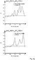
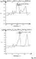
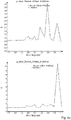
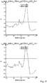
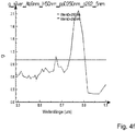
- FIGS. 4a to 4l Selected simulation results concerning the calculated absorption increases g as a function of the wavelength are given in FIGS FIGS. 4a to 4l summarized. As can be seen from the individual representations, some show strong absorption increases in preferred wavelength ranges.
- the properties of the plasmons in the antireflection layers thus not only enable improved photon management, but also, using special design parameters, an optical filter function or signal attenuation and a simultaneous amplification of specific frequency ranges can be achieved.
- the nano-antenna elements 22 can be adapted accordingly with respect to their design parameters to effect special properties in the range of optical sensors.
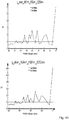
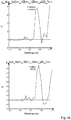
- FIG. 4a shows simulation results for the cross structure according to series 11 according to Table 1.
- the representation of the absorption increase as a function of the wavelength shows two strong peaks at about 1050 nanometers and 725 nanometers with an up to 6-fold gain.
- the remaining frequency range remains unaffected or only relatively weakly amplified up to a range of approximately 550 nanometers.
- the position of the peaks or their height can be influenced by the design parameters.
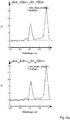
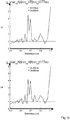
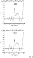
- Fig. 4b shows simulation results for the cross structure according to series 12 and 13. It can be seen that there are two strong peaks at 1050 and 825 nanometers, with up to a 16-fold gain. The remaining frequency range remains unaffected or only relatively weakly amplified. The position of the peaks or their height can be influenced by the design parameters.
- Fig. 4c shows further simulation results for the cross structure according to series 16.
- the remaining frequency range remains unaffected or only relatively weakly amplified up to a range of approximately 550 nanometers.
- the position of the peaks or their height can be influenced by the design parameters.
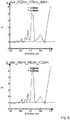
- Fig. 4d shows simulation results for the cross structure according to series 15. It can be seen that there are two very strong peaks at about 1000 nanometers and about 750 nanometers, with up to a 4-fold gain. The remaining frequency range remains unaffected or only relatively weakly amplified up to a range of approximately 550 nanometers. The position of the peaks or their height can be influenced by the design parameters.
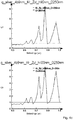
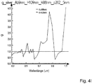
- Fig. 4e shows simulation results for the triangular structure according to series 17. It can be seen that a very strong peak occurs at about 1050 nanometers with up to a 19-fold gain. The remaining frequency range remains unaffected or only relatively weakly amplified. The position of the peaks or their height can be influenced by the design parameters.
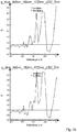
- Fig. 4f shows simulation results for the star structure according to series 6 and 7. It can be seen that a very strong peak at about 825 nanometers means a gain of up to 3.3 times. The remaining frequency range remains unaffected or only relatively weakly amplified. The position of the peaks or their height can be influenced by the design parameters.
- Fig. 4g to l shows simulation results for the square structure according to series 8. There are three strong peaks at about 1100 nanometers, 850 nanometers and 725 nanometers with up to 7-fold amplification. The remaining frequency range remains unaffected or only relatively weakly amplified. The position of the peaks or their height can be influenced by the design parameters.
- the absorption properties can be specifically influenced in order to amplify certain frequency ranges, which is advantageous for use as a sensor.
- the antenna elements 22 are cylindrical in orthogonal configuration with a period of 525 nanometers.
- the radius is 125 nanometers and the height h is 70 nanometers.
- the distance d from the absorber layer 12 is 9 nanometers.
- the radius of the cylinders is 95 nanometers and the height h is 70 nanometers.
- the distance d from the absorber layer 12 is 9 nanometers.
- the period is optimally 490 nanometers.
Description
Die Erfindung betrifft eine Photozelle, insbesondere eine Solarzelle, mit einer Absorberschicht, vor eine der Antireflexionsschicht angeordnet ist.The invention relates to a photocell, in particular a solar cell, with an absorber layer, is arranged in front of one of the antireflection layer.
Bei der Herstellung von Solarzellen wird weltweit seit Jahren daran gearbeitet, den Wirkungsgrad zu erhöhen. Solarzellen werden bislang überwiegend aus Silizium hergestellt, wobei Standard-Dickschicht-Solarzellen meist eine Dicke in der Größenordnung von bis zu 200 Mikrometer haben und aus monokristallinem Silizium hergestellt werden. Während bei monokristallinen Solarzellen das Silizium von hoher Qualität und defektfrei sein muss, sind in jüngerer Zeit auch Dünnschichtsolarzellen mit Dicken von wenigen Mikrometern oder sogar darunter in der Entwicklung.In the production of solar cells has been working worldwide for years to increase the efficiency. Solar cells have hitherto been predominantly made of silicon, with standard thick-film solar cells usually having a thickness of the order of magnitude of up to 200 micrometers and being produced from monocrystalline silicon. While in monocrystalline solar cells the silicon must be of high quality and defect-free, thin-film solar cells with thicknesses of a few micrometers or even less are currently being developed.
Bei der Wirkungsgraderhöhung von Solarzellen geht es im Wesentlichen um zwei physikalisch unabhängige Prozesse:
- Zum Einen geht es darum, das Licht optimal in die Zelle einzukoppeln und solange wie möglich in der Zelle zu halten, d.h. so viele Photonen wie möglich sollen in der Zelle absorbiert werden. Es geht also um ein optimiertes Photonen-Management.
- Zum anderen geht es darum, die generierten elektrischen Ladungen (nach der Lichtabsorption) so gut wie möglich aus der Zelle zum Verbraucher zu bringen. Es geht also darum, Verlustprozesse zu minimieren, d.h. es geht um ein verbessertes Elektronen-Management.
- On the one hand it is about optimally coupling the light into the cell and keeping it in the cell as long as possible, ie as many photons as possible should be absorbed in the cell. So it's about optimized photon management.
- On the other hand, the aim is to bring the generated electrical charges (after light absorption) as much as possible from the cell to the consumer. It is therefore about minimizing loss processes, ie it is about improved electron management.
Jede Verbesserung im Photonen-Management erhöht die Anzahl der absorbierten Photonen in der Solarzelle unmittelbar. Je besser also das Photonen-Management ist, desto höher ist die Effizienz der Solarzelle unabhängig vom aktuellen Elektronen-Management der Zelle.Any improvement in photon management directly increases the number of photons absorbed in the solar cell. Thus, the better the photon management, the higher the efficiency of the solar cell regardless of the cell's current electron management.
Um die Absorption bei Solarzellen zu erhöhen, wird standardmäßig eine Antireflexionsschicht (AR-Schicht) verwendet, die geometrisch strukturiert ist, und zwar in Form einer Pyramidenstruktur oder einer invertierten Pyramidenstruktur. Hierdurch wird eine deutliche Verbesserung im Photonen-Management von Solarzellen erzielt und dadurch der Wirkungsgrad um etwa 10 % (relativ) verbessert, d.h. eine Solarzelle mit z.B. 20 % Wirkungsgrad kann durch die Verwendung einer AR-Schicht mit Pyramidenstruktur im Wirkungsgrad auf 22 % gesteigert werden.To increase the absorption in solar cells, an antireflection layer (AR layer) is used by default, which is geometrically structured, in the form of a pyramidal structure or an inverted pyramidal structure. This achieves a significant improvement in the photon management of solar cells, thereby improving the efficiency by about 10% (relative), i. a solar cell with e.g. 20% efficiency can be increased to 22% efficiency by using an AR layer with pyramidal structure.
Die AR-Schicht besteht in der Regel aus Siliziumnitrid und ist als eine regelmäßige Pyramidenstruktur ausgebildet, wobei die Basis der quadratischen Pyramiden meist 2 bis 10 Mikrometer lang ist. Der Spitzenwinkel der Pyramiden mit quadratischer Grundfläche liegt bei etwa 70°.The AR layer is usually made of silicon nitride and is formed as a regular pyramidal structure, wherein the base of the square pyramids is usually 2 to 10 microns long. The apex angle of the pyramids with a square base is about 70 °.
Nachteilig bei derartigen AR-Schichten ist insbesondere, dass die Struktur nur in einem sehr schmalen Wellenlängenbereich des Sonnenspektrums optimal arbeitet.A disadvantage of such AR layers is in particular that the structure works optimally only in a very narrow wavelength range of the solar spectrum.
Aus diesem Grunde wird versucht, ein verbessertes Photonen-Management durch plasmonische Strukturen zu erreichen.For this reason, attempts are being made to achieve improved photon management by plasmonic structures.
Gemäß
Ein erster Ansatz zur Verbesserung von Solarzellen durch plasmonische Strukturen bestand hiernach darin, bei einer herkömmlichen Siliziumsolarzelle zusätzlich auf der Oberfläche Nanopartikel aufzubringen, was durch Abscheiden einer dünnen Metallschicht und Glühen unter Stickstoff erfolgt, so dass sich die Struktur in diskrete Inseln umwandelte. Die sich ergebenden Strukturen waren allerdings irregulär. Gemäß einem zweiten Ansatz wurden kolloidale Silber- und Gold-Nanopartikel als Quelle von Streuelementen verwendet. Dies führte zu einer gleichförmigen Größe und einer gleichförmigen Dichteverteilung von Partikeln auf der Oberfläche. Diese Abscheidungsart wurde bei kristallinem Silizium, amorphem Silizium und InP/InGaAsP-Zellen verwendet. Teilweise wurde eine Wirkungsgradverbesserung von 8 % bei Silber-Nanopartikeln beobachtet. Weiterhin wurden die Auswirkungen der Größe und Dichteverteilung von Nanopartikeln auf GaAs-Solarzellen unter Verwendung von AAO-Masken ("anodic aluminum oxide") als Verdampfungsmasken als ein Mittel zur Kontrolle der Höhe und Dichte der abgeschiedenen Nanopartikeln untersucht. Die höchsten Wirkungsgraderhöhungen wurden bei dichten, hohen Anordnungen von Partikeln beobachtet, was auf die Nahfeld-Kopplung zwischen den Partikeln zurückgeführt wurde.A first approach for improving solar cells by plasmonic structures was therefore to additionally apply nanoparticles to the surface of a conventional silicon solar cell, which is done by depositing a thin metal layer and annealing under nitrogen, so that the structure is transformed into discrete islands. The resulting structures, however, were irregular. In a second approach, colloidal silver and gold nanoparticles were used as the source of scattering elements. This resulted in a uniform size and uniform density distribution of particles on the surface. This type of deposition has been used on crystalline silicon, amorphous silicon and InP / InGaAsP cells. In some cases, an improvement in efficiency of 8% was observed for silver nanoparticles. Furthermore, the effects of size and density distribution of nanoparticles on GaAs solar cells were investigated using AAO masks ("anodic aluminum oxide") as evaporation masks as a means of controlling the height and density of the deposited nanoparticles. The highest increases in efficiency were observed in dense, high particle arrangements, which was attributed to near-field coupling between the particles.
Es wurde auch die Auswirkung einer nanostrukturierten AR-Schicht aus Silber auf der Oberfläche des Siliziums untersucht. Bei den nanostrukturierten Streuobjekten handelte es sich um Rippen von 100 Nanometer Breite und 50 Nanometer Höhe, ausgehend von der Rückseite der Zelle in den Halbleiter. Es wurden sowohl Abstände von 6 Mikrometer als auch von 300 Nanometer untersucht und hierbei gewisse Absorptionsverbesserungen festgestellt.The effect of a nanostructured AR layer of silver on the surface of silicon was also investigated. The nanostructured scattering objects were fins 100 nanometers wide and 50 nanometers high, starting from the back of the cell into the semiconductor. Both 6 micron and 300 nanometer distances were investigated, and certain absorption improvements were observed.
Gemäß
Zur großflächigen Herstellung von plasmonischen Solarzellenstrukturen wurde die Formung von metallischen Nanopartikeln durch thermisches Verdampfen einer dünnen Metallschicht in Betracht gezogen, die anschließend beheizt wird, um Agglomerate auf der Oberfläche zu bilden. Dies führte zu unregelmäßig angeordneten Nanopartikeln mit einem Durchmesser von 100 bis 150 Nanometer. Durch Lithographie mit einem Stempel, bei der eine Sol-Gel-Maske durch Weichlithographie unter Verwendung eines Gummistempels, gefolgt von Silberaufdampfung und anschließendem Ablösen, soll eine Auflösung von < 0,1 Nanometer erzielt werden. Hierdurch wurden hexagonale Arrays aus Silber-Nanopartikeln mit einem Partikeldurchmesser von 300 Nanometer und etwa halbkugelförmiger Gestalt mit einem Abstand von etwa 500 Nanometern erzeugt.For the large-scale production of plasmonic solar cell structures, the formation of metallic nanoparticles by thermal evaporation of a thin metal layer was considered, which is then heated to form agglomerates on the surface. This resulted in irregularly arranged nanoparticles with a diameter of 100 to 150 nanometers. By lithography with a stamp, in which a sol-gel mask by soft lithography using a rubber stamp, followed by silver vapor deposition and subsequent peeling, a resolution of <0.1 nanometer is to be achieved. As a result, hexagonal arrays of silver nanoparticles with a particle diameter of 300 nanometers and approximately hemispherical shape with a spacing of about 500 nanometers were generated.
Die herkömmlichen Strukturen mit optischen Antireflexionsschichten in Pyramidenform und auch die neueren Ansätze mit plasmonischen Strukturen liefern zwar vereinzelt Verbesserungen des Photonen-Managements, sind jedoch noch nicht ausreichend weit entwickelt, um deutliche Verbesserungen zu gewährleisten.Although the conventional structure with pyramid-shaped optical antireflection layers and also the more recent approaches with plasmonic structures provide occasional improvements in photon management, they are not yet sufficiently developed to ensure significant improvements.
Aus
Aus der
Ferner sei auf die
Vor diesem Hintergrund liegt der Erfindung die Aufgabe zugrunde, eine verbesserte Photozelle, insbesondere Solarzelle, anzugeben, mit der eine merkliche Verbesserung des Photonen-Managements erzielt werden kann.Against this background, the invention has for its object to provide an improved photocell, in particular solar cell, with which a significant improvement in the photon management can be achieved.
Diese Aufgabe wird erfindungsgemäß durch eine Photozelle, insbesondere eine Solarzelle, mit den Merkmalen des Anspruchs 1 gelöst.This object is achieved by a photocell, in particular a solar cell, with the features of
Die Aufgabe der Erfindung wird auf diese Weise vollkommen gelöst.The object of the invention is completely solved in this way.
Erfindungsgemäß wird durch die Verwendung einer nanostrukturierten Schicht mit periodisch angeordneten Antennenelementen aus einem elektrisch leitfähigen Material, die in einem Abstand von 1 bis 50 Nanometer von der Absorberschicht angeordnet ist, wobei die Antennenelemente mit einem Abstand von mehr als 250 bis 750 Nanometern zueinander angeordnet sind und eine Höhe von mehr als 30 bis 120 Nanometern aufweisen, eine deutliche Verbesserung des Photonen-Managements erreicht, d.h. insgesamt eine deutliche Verbesserung der Absorption in der Solarzelle. Die Antennenelemente können das gesamte Sonnenlichtspektrum (von 280 Nanometer bis 1100 Nanometer Wellenlänge) breitbandig gut in die Solarzelle einkoppeln und das Licht länger in der Solarzelle halten, als die bisher verwendeten Mikrostrukturen, da die Nano-Antennenelemente das absorbierte Licht in der Solarzelle wieder aufnehmen (empfangen) und in die Solarzelle zurückstrahlen. Auf diese Weise kann mit der neuartigen nanostrukturierten Schicht das Licht etwa um einen Faktor von 2 besser absorbiert werden als mit herkömmlichen AR-Schichten in Pyramidenform (der Wirkungsgrad kann um etwa 20% (relativ) verbessert werden). Bei der erfindungsgemäßen nanostrukturierten Schicht mit periodisch angeordneten Antennenelementen wirken diese als Oberflächenplasmonen mit definierten Nahfeldeigenschaften. Die nanostrukturierte Schicht bildet zusammen mit einem Rückkontakt der Photozelle einen optischen Resonator.According to the invention, the use of a nanostructured layer with periodically arranged antenna elements of an electrically conductive material, which is arranged at a distance of 1 to 50 nanometers from the absorber layer, wherein the antenna elements are arranged with a distance of more than 250 to 750 nanometers to each other and have a height of more than 30 to 120 nanometers, achieved a significant improvement in photon management, ie Overall, a significant improvement in the absorption in the solar cell. The antenna elements can easily couple the entire spectrum of sunlight (from 280 nm to 1100 nm wavelength) into the solar cell and hold the light longer in the solar cell than the previously used microstructures since the nano-antenna elements resume the absorbed light in the solar cell ( received) and radiate back into the solar cell. In this way, with the novel nanostructured layer, the light can be better absorbed by a factor of 2 than with conventional AR layers in pyramidal form (the efficiency can be improved by about 20% (relative)). In the case of the nanostructured layer according to the invention with periodically arranged antenna elements, these act as surface plasmons with defined near-field properties. The nanostructured layer forms an optical resonator together with a back contact of the photocell.
Die im Stand der Technik bisher bekannten Plasmonen-Strukturen mit nanostrukturierten Schichten weisen entweder keine periodisch angeordneten Antennenelemente auf oder sind noch dermaßen unbestimmt, dass sich keine optimierten Eigenschaften über einen weiten Bereich erzielen lassen.The plasmon structures with nanostructured layers known hitherto in the prior art either have no periodically arranged antenna elements or are still so indeterminate that no optimized properties can be achieved over a wide range.
Ein besonderer Vorteil der erfindungsgemäßen Photozelle besteht darin, dass die nanostrukturierte Schicht mit periodisch angeordneten Antennenelementen bei allen Arten von Photozellen unabhängig vom Aufbau der Photozelle selbst verwendbar ist.A particular advantage of the photocell according to the invention is that the nanostructured layer can be used with periodically arranged antenna elements in all types of photocells regardless of the structure of the photocell itself.
Bei den erfindungsgemäßen Photozellen wird das Licht über einen größeren Winkelbereich eingesammelt und in das Substrat eingestrahlt, da die Plasmonen als Antennen wirken. Auch wird eine Unschärfe bei Bestrahlung mit Infrarotlicht durch Modenbildung reduziert. Die Moden bilden sich nämlich auch in Bereichen der Sensorschicht aus, wodurch ein verbessertes Einsammeln der erzeugten Elektronen möglich ist.In the photocells according to the invention, the light is collected over a larger angular range and irradiated into the substrate, since the plasmons act as antennas. Also, blurring upon irradiation with infrared light is reduced by patterning. Namely, the modes are also formed in regions of the sensor layer, whereby an improved collection of the generated electrons is possible.
Gemäß einer weiteren Ausgestaltung der Erfindung ist die nanostrukturierte Schicht mit einem Abstand von 2 bis 20 Nanometer von der Absorberschicht angeordnet, vorzugsweise mit einem Abstand von 5 bis 15 Nanometer, besonders bevorzugt mit einem Abstand von 7 bis 12 Nanometer.According to a further embodiment of the invention, the nanostructured layer is arranged at a distance of 2 to 20 nanometers from the absorber layer, preferably at a distance of 5 to 15 nanometers, particularly preferably at a distance of 7 to 12 nanometers.
Es hat sich gezeigt, dass mit einem derartigen Abstand besonders gute Eigenschaften, insbesondere eine besonders gute Absorptionsverbesserung über einen weiten Wellenlängenbereich erzielt werden können.It has been shown that with such a distance particularly good properties, in particular a particularly good absorption improvement over a wide wavelength range can be achieved.
Einzelne Antennenelemente sind vorzugsweise entweder orthogonal oder hexagonal zueinander periodisch angeordnet.Individual antenna elements are preferably arranged periodically either orthogonal or hexagonal to one another.
Die maximale Ausdehnung der Antennenelemente in Querrichtung beträgt vorzugsweise 20 bis 400 Nanometer, weiter bevorzugt 40 bis 250 Nanometer, besonders bevorzugt 100 bis 250 Nanometer.The maximum extension of the antenna elements in the transverse direction is preferably 20 to 400 nanometers, more preferably 40 to 250 nanometers, particularly preferably 100 to 250 nanometers.
Die minimale Ausdehnung der Antennenelemente in Querrichtung beträgt vorzugsweise 25 Nanometer, weiter bevorzugt 30 Nanometer, besonders bevorzugt mindestens 50 Nanometer.The minimum extension of the antenna elements in the transverse direction is preferably 25 nanometers, more preferably 30 nanometers, particularly preferably at least 50 nanometers.
Mit einer derartigen Dimensionierung können besonders vorteilhafte Eigenschaften in weiten Bereichen insbesondere an bestimmte Zellstrukturen angepasst werden, um insgesamt eine verbesserte Absorption über ein bestimmtes Frequenzspektrum zu erreichen, oder um ggf. besondere Frequenzbereiche besonders zu verstärken, so dass auch ein Einsatz als Photozellen im Bereich der optischen Sensoren möglich ist.With such a dimensioning, particularly advantageous properties can be adapted in a wide range, in particular to specific cell structures, in order to achieve improved absorption over a particular frequency spectrum or, if necessary, to particularly enhance particular frequency ranges, so that use as photocells in the region of optical sensors is possible.
Die nanostrukturierte Schicht mit den Antennenelementen ist vorzugsweise zumindest teilweise in der Antireflexionsschicht aufgenommen, die vorzugsweise aus SiOxNy (beispielsweise SiO3N4), Titanoxid oder ITO ("Indium-Tin-Oxide") besteht. Soweit die nanostrukturierte Schicht infolge ihrer Höhe aus der Antireflexionsschicht teilweise hervorsteht, liegt diese vorzugsweise in einer darüber aufgebrachten Schutzschicht, die etwa aus Siliziumoxid bestehen kann.The nanostructured layer with the antenna elements is preferably at least partially accommodated in the antireflection layer, which preferably consists of SiOxNy (for example SiO3N4), titanium oxide or ITO ("indium tin oxide"). Insofar as the nanostructured layer partially protrudes from the antireflection coating as a result of its height, it preferably lies in a protective layer applied over it, which may be made of silicon oxide, for example.
Die nanostrukturierte Schicht kann aus identischen Antennenelementen bestehen oder auch aus Antennenelementen unterschiedlicher Form und/oder Größe, die in einem regelmäßigen Muster miteinander kombiniert sind.The nanostructured layer can consist of identical antenna elements or of antenna elements of different shape and / or size, which are combined with each other in a regular pattern.
Gemäß einer weiteren Ausgestaltung der Erfindung besteht die nanostrukturierte Schicht aus kreisförmigen, vieleckförmigen, dreieckförmigen oder quadratischen Antennenelementen, aus kreuzförmigen Antennenelementen, in Form von miteinander gekreuzten Balken in symmetrischer Ausgestaltung, in Form eines Quadrats mit kleineren an jeder Außenseite angesetzten Quadraten in symmetrischer Ausgestaltung, in Form eines Quadrates mit quadratischen Aussparungen in jedem Eckbereich in symmetrischer Ausgestaltung, oder in Form eines Kreises mit vier tangential aufgesetzten Rechtecken in symmetrischer Ausgestaltung, wobei die Rechtecke entweder in Richtung einer Elementarzelle angeordnet sind oder um 45° versetzt dazu, oder besteht aus sternförmigen Elementen mit sechs Spitzen, die hexagonal auf einer Elementarzelle angeordnet sind, wobei jeweils die Spitzen der sternförmigen Antennenelemente zueinander zeigen oder die Seiten zwischen den Spitzen zueinander zeigen.According to a further embodiment of the invention, the nanostructured layer consists of circular, polygonal, triangular or square antenna elements, of cross-shaped antenna elements, in the form of crossed bars in a symmetrical configuration, in the form of a square with smaller squares on each outer side in a symmetrical configuration, in Shape of a square with square recesses in each corner region in a symmetrical configuration, or in the form of a circle with four tangentially patched rectangles in a symmetrical configuration, the rectangles are either arranged in the direction of a unit cell or offset by 45 ° thereto, or consists of star-shaped elements six peaks arranged hexagonally on a unit cell, with the tips of the star-shaped antenna elements facing each other or the sides between the peaks facing each other.
Mit derartigen Antennenelementen lässt sich in Abhängigkeit vom jeweiligen Anwendungsfall, d.h. insbesondere eine Absorptionsverbesserung bei einer bestimmten Solarzelle, oder eine gezielte Verstärkung eines bestimmten Frequenzbereiches, oder Filterung eines bestimmten Frequenzbereiches bei einer Anwendung als Sensor erreichen.With such antenna elements, depending on the particular application, ie in particular an absorption improvement in a particular solar cell, or a targeted amplification of a particular frequency range, or filtering a certain frequency range in an application as a sensor reach.
Vorzugsweise sind die Antennenelemente als Zylinder oder als gerade Prismen ausgebildet, die sich senkrecht zu einer Haupterstreckungsrichtung der Photozelle erstrecken.Preferably, the antenna elements are formed as cylinders or as straight prisms, which extend perpendicular to a main extension direction of the photocell.
Weiter bevorzugt bestehen die Antennenelemente aus einem Metall, das aus der Gruppe ausgewählt ist, die Silber, Kupfer, Aluminium, Gold und deren Legierungen enthält.More preferably, the antenna elements are made of a metal selected from the group consisting of silver, copper, aluminum, gold and their alloys.
In den meisten Fällen ist Silber besonders bevorzugt, jedoch können für einzelne Anwendungen auch andere Metalle vorteilhaft sein.In most cases, silver is particularly preferred, but other metals may be advantageous for individual applications.
Gemäß einer weiteren Ausgestaltung der Erfindung bestehen die Antennenelemente aus einem Metall, das aus der Gruppe ausgewählt ist, die Silber, Kupfer, Aluminium, Gold und deren Legierungen enthält, und wobei zumindest eine dem Absorber zugewandte oder dem Absorber abgewandte Seite der Antennenelemente mit einem anderen Metall beschichtet ist, das aus der Gruppe ausgewählt ist, die Silber, Kupfer, Aluminium, Gold und deren Legierungen enthält.According to a further embodiment of the invention, the antenna elements are made of a metal selected from the group consisting of silver, copper, aluminum, gold and their alloys, and at least one side of the antenna elements facing the absorber or the absorber facing away from one another Metal selected from the group consisting of silver, copper, aluminum, gold and their alloys.
Durch eine derartige Beschichtung der Antennenelemente auf der einen oder der anderen Seite oder auf beiden Seiten, können gezielte Eigenschaftsverbesserungen erreicht werden.By such a coating of the antenna elements on one or the other side or on both sides, targeted property improvements can be achieved.
Gemäß einer weiteren Ausgestaltung der Erfindung besteht die nanostrukturierte Schicht aus geraden Zylindern. Dieses ist insbesondere dann vorteilhaft, wenn die Photozelle als Solarzelle, insbesondere als Siliziumsolarzelle ausgestaltet ist.According to a further embodiment of the invention, the nanostructured layer consists of straight cylinders. This is particularly advantageous when the photocell is designed as a solar cell, in particular as a silicon solar cell.
Es hat sich gezeigt, dass durch die Ausgestaltung der nanostrukturierten Schicht mit geraden Zylindern sich eine besonders gute Absorptionserhöhung über den gesamten Spektralbereich des Sonnenlichtes erzielen lässt.It has been shown that the configuration of the nanostructured layer with straight cylinders can achieve a particularly good increase in absorption over the entire spectral range of the sunlight.
Gemäß einer Weiterbildung dieser Ausführung besteht die nanostrukturierte Schicht aus Zylindern mit einem Durchmesser von 150 bis 250 Nanometern, vorzugsweise von 180 bis 200 Nanometern, und mit einer Höhe von 50 bis 90 Nanometern, die vorzugsweise in einem orthogonalen Muster mit einem Abstand von 400 bis 600 Nanometern, vorzugsweise 450 bis 510 Nanometern angeordnet sind und einen Abstand zur Absorberschicht von 5 bis 13 Nanometern, vorzugsweise von 8 bis 10 Nanometern, aufweisen.According to a development of this embodiment, the nanostructured layer consists of cylinders with a diameter of 150 to 250 nanometers, preferably from 180 to 200 nanometers, and with a height of 50 to 90 nanometers, which are preferably arranged in an orthogonal pattern with a spacing of 400 to 600 nanometers, preferably 450 to 510 nanometers and a distance to the absorber layer of 5 to 13 nanometers, preferably from 8 to 10 nanometers.
Hiermit ergeben sich optimale Eigenschaften für Standard-Solarzellen, d.h. monokristalline Solarzellen, mit einer Dicke von etwa 180 bis 200 Mikrometer.This results in optimum properties for standard solar cells, i. monocrystalline solar cells, having a thickness of about 180 to 200 microns.
In weiter bevorzugter Ausgestaltung der Erfindung ist die Solarzelle als Standard-Dickschicht-Solarzelle mit einer Dicke von bis zu 200 Mikrometer ausgebildet, wobei die Zylinder der nanostrukturierten Schicht einen Durchmesser von 185 bis 195 Nanometern, vorzugsweise etwa 190 Nanometer, haben, eine Höhe von 68 bis 72 Nanometern, vorzugsweise etwa 70 Nanometer, einen Abstand zur Absorberschicht von 8,5 bis 9,5 Nanometern, vorzugsweise etwa 9 Nanometer, aufweisen und mit einem Abstand von 460 bis 470 Nanometern, vorzugsweise etwa 465 Nanometer, in einem orthogonalen Muster zueinander angeordnet sind.In a further preferred embodiment of the invention, the solar cell is designed as a standard thick-film solar cell with a thickness of up to 200 micrometers, wherein the cylinders of the nanostructured layer have a diameter of 185 to 195 nanometers, preferably about 190 nanometers, a height of 68 to 72 nanometers, preferably about 70 nanometers, have a distance to the absorber layer of 8.5 to 9.5 nanometers, preferably about 9 nanometers, and arranged at a distance of 460 to 470 nanometers, preferably about 465 nanometers, in an orthogonal pattern to each other are.
Hiermit ergeben sich optimale Bedingungen für eine Standard-Dickschicht-Solarzelle.This results in optimum conditions for a standard thick-film solar cell.
Gemäß einer weiteren Ausgestaltung der Erfindung ist die Solarzelle als HIT-Dickschicht-Solarzelle mit einer Dicke von bis zu 200 Mikrometer ausgebildet, wobei die Zylinder der nanostrukturierten Schicht einen Durchmesser von etwa 185 bis 195 Nanometern, vorzugsweise etwa 190 Nanometer, haben, eine Höhe von 68 bis 72 Nanometern, vorzugsweise etwa 70 Nanometer, einen Abstand zur Absorberschicht von 8,5 bis 9,5 Nanometern, vorzugsweise etwa 9 Nanometer aufweisen und mit einem Abstand von 485 bis 495 Nanometern, vorzugsweise etwa 490 Nanometer, in einem orthogonalen Muster zueinander angeordnet sind. Hiermit ergeben sich optimale Eigenschaften für eine HIT-Dickschicht-Solarzelle ("hetero junction with intrinsic thin layer"-HIT).According to a further embodiment of the invention, the solar cell is designed as a HIT thick-film solar cell with a thickness of up to 200 micrometers, wherein the cylinders of the nanostructured layer have a diameter of about 185 to 195 nanometers, preferably about 190 nanometers, a height of 68 to 72 nanometers, preferably about 70 nanometers, have a distance to the absorber layer of 8.5 to 9.5 nanometers, preferably about 9 nanometers and arranged at a distance of 485 to 495 nanometers, preferably about 490 nanometers, in an orthogonal pattern to each other are. This results in optimum properties for a HIT thick-film solar cell (heterojunction with intrinsic thin layer HIT).
Bei einer Ultradünnschichtsolarzelle besteht die nanostrukturierte Schicht vorteilhaft aus Zylindern mit einem Durchmesser von 200 bis 300 Nanometern, vorzugsweise etwa 250 Nanometern, mit einer Höhe von 50 bis 90 Nanometern, vorzugsweise etwa 70 Nanometern, die vorzugsweise in einem orthogonalen Muster mit einem Abstand von 400 bis 600 Nanometern, vorzugsweise etwa 525 Nanometern angeordnet sind und einen Abstand zur Absorberschicht von 5 bis 13 Nanometern, vorzugsweise von etwa 9 Nanometern, aufweisen.In the case of an ultrathin-film solar cell, the nanostructured layer advantageously consists of cylinders with a diameter of 200 to 300 nanometers, preferably about 250 nanometers, with a height of 50 to 90 nanometers, preferably about 70 nanometers, preferably in an orthogonal pattern with a spacing of 400 to 600 nanometers, preferably about 525 nanometers are arranged and have a distance to the absorber layer of 5 to 13 nanometers, preferably of about 9 nanometers.
Hiermit ergeben sich optimale Bedingungen bezüglich einer Ultradünnschichtsolarzelle.This results in optimum conditions with respect to an ultrathin-film solar cell.
Bei der Ultradünnschichtsolarzelle kann es sich beispielsweise um eine Zelle etwa mit einer Dicke in der Größenordnung von bis zu etwa 1000 Nanometern, bspw. mit einer Rückkontaktschicht aus Silber und einer Stärke von 200 Nanometern, einer Absorberschicht aus Silizium mit einer Stärke von etwa 150 Nanometern, einer AR-Schicht etwa aus Siliziumnitrid mit einer Stärke von etwa 45 Nanometern und einer Schutzschicht aus Siliziumdioxid mit einer Stärke von etwa 64 Nanometern, handeln.The ultrathin-film solar cell can be, for example, a cell approximately in the order of up to about 1000 nanometers in thickness, for example with a back contact layer of silver and a thickness of 200 nanometers, an absorber layer of silicon with a thickness of approximately 150 nanometers, For example, an AR layer may be about 45 nanometers thick silicon nitride and about 64 nanometers thick silicon dioxide protective layer.
Gemäß einer weiteren Ausgestaltung der Erfindung wird die Photozelle als Solarzelle mit einer Absorptionserhöhung ausgewählter Frequenzbereiche einfallender Strahlung verwendet.According to a further embodiment of the invention, the photocell is used as a solar cell with an absorption increase of selected frequency ranges of incident radiation.
Es lassen sich also insbesondere in Abhängigkeit von der Dicke der Solarzelle eine Absorptionserhöhung bezüglich ausgewählter Frequenzbereiche einfallender Strahlung verwirklichen, um etwa IR-Anteile, die teilweise ungenutzt sind, verstärkt zu nutzen, so dass sich eine insgesamt gleichmäßige Ausnutzung der Strahlung über das gesamte Frequenzband des einfallenden Lichtes ergibt.In particular, depending on the thickness of the solar cell, it is thus possible to realize an increase in absorption with respect to selected frequency ranges of incident radiation, in order to make greater use of IR components which are partially unused, so that overall uniform utilization of the radiation over the entire frequency band of the solar cell is achieved incident light.
Gemäß einer weiteren Ausgestaltung der Erfindung wird die Photozelle als Sensor verwendet, mit einer Absorptionserhöhung ausgewählter Frequenzbereiche und/oder einer optischen Signalschwächung über einen bestimmten Frequenzbereich.According to a further embodiment of the invention, the photocell is used as a sensor, with an absorption increase of selected frequency ranges and / or an optical signal attenuation over a certain frequency range.
In Abhängigkeit von den gewählten Parametern der nanostrukturierten Schicht lassen sich die Eigenschaften in weiten Grenzen variieren, um bestimmte Absorptionserhöhungen ausgewählter Frequenzbereiche zu erhalten, also um etwa besondere Verstärkungen in einzelnen Frequenzbereichen zu bewirken. Umgekehrt können auch optische Signalschwächungen über einen bestimmten Frequenzbereich, also optische Filterfunktionen, erreicht werden.Depending on the selected parameters of the nanostructured layer, the properties can be varied within wide limits, in order to obtain certain absorption increases of selected frequency ranges, ie to effect, for example, particular gains in individual frequency ranges. Conversely, optical signal attenuation over a certain frequency range, ie optical filter functions, can be achieved.
Eine erfindungsgemäße Photozelle kann vorteilhaft hergestellt werden, indem die Photozelle mit einem Absorber und mit einer darüber angeordneten Antireflexionsschicht (unstrukturiert) hergestellt wird, wobei die Antireflexionsschicht mit einer nanostrukturierten Schicht mit periodisch angeordneten Antennenelementen aus einem elektrisch leitfähigem Material mit einem Abstand von 1 bis 50 Nanometern zur Absorberoberfläche hergestellt wird.A photocell according to the invention can advantageously be produced by producing the photocell with an absorber and an antireflection layer (unstructured) arranged above it, the antireflection layer having a nanostructured layer with periodically arranged antenna elements made of an electrically conductive material with a spacing of 1 to 50 nanometers is made to the absorber surface.
Hierbei werden vorteilhaft, zumindest Form, Größe, Anordnung, Periodizität und Abstand der Antennenelemente von der Absorberfläche in Abhängigkeit vom Aufbau und den Designparametern der Photozelle angepasst, um eine gezielte Absorptionserhöhung in einem gewünschten ersten Frequenzbereich und/oder eine optische Signalschwächung über einen zweiten Frequenzbereich zu gewährleisten.Advantageously, at least the shape, size, arrangement, periodicity and spacing of the antenna elements are adapted to the absorber surface as a function of the design and the design parameters of the photocell to a targeted increase in absorption in a desired first frequency range and / or optical signal attenuation over a second frequency range guarantee.
Durch eine Anpassung der Antennenelemente lassen sich sozusagen die Eigenschaften der nanostrukturierten Schicht im Hinblick auf die gewünschte Anwendung maßschneidern.By adapting the antenna elements, so to speak, the properties of the nanostructured layer can be tailor-made with regard to the desired application.
Eine Herstellung der nanostrukturierten Schicht erfolgt mit grundsätzlich bekannten Verfahren, die im Hinblick auf die gewünschte Anwendung angepasst werden.A production of the nanostructured layer is carried out by basically known methods, which are adapted with regard to the desired application.
Bei einem Verfahren zum Herstellen einer Photozelle der vorstehend beschriebenen Art umfasst die Herstellung der nanostrukturierten Schicht nach der Applikation der (unstrukturierten) Absorberschicht und einer Schutzschicht zumindest die folgenden Schritte:
- Auftragen einer Photolackschicht auf die Schutzschicht;
- Prägen der Photolackschicht mittels eines nanostrukturierten Stempels;
- Entwickeln der Photolackschicht durch Bestrahlen mittels UV-Licht zur Erzeugung einer nanostrukturierten Photolackschicht;
- Ätzen zur Erzeugung von Vertiefungen;
- flächiges Beschichten der nanostrukturierten Schicht mit einem elektrisch leitfähigen Material;
- Entfernen der Photolackschicht.
- Applying a photoresist layer to the protective layer;
- Embossing the photoresist layer by means of a nanostructured stamp;
- Developing the photoresist layer by irradiation with UV light to form a nanostructured photoresist layer;
- Etching to create pits;
- planar coating of the nanostructured layer with an electrically conductive material;
- Removing the photoresist layer.
Es handelt sich hierbei um das Herstellen der nanostrukturierten Schicht durch ein Nano-Imprint-Verfahren, nämlich die sog. Nanoprägelithographie. Hierbei wird ein weicher Prägestempel bei Raumtemperatur verwendet. Die Kontaktkraft ist kleiner als 1000 Newton. Bei der Entwicklung der Photolackschicht wird UV-Licht mit einem Wellenlängenbereich von 350 bis 450 Nanometer verwendet. Es lassen sich Auflösungen von < 15 Nanometer erzielen und Substrate von 10 bis 200 mm bearbeiten. Es handelt sich um die sog. UV-Nano-Imprint-Lithographie (UV-NIL).This involves the production of the nanostructured layer by a nanoimprint process, namely the so-called nanoprint lithography. Here, a soft die is used at room temperature. The contact force is less than 1000 Newton. In the development of the photoresist layer, UV light with a wavelength range of 350 to 450 nanometers is used. It can achieve resolutions of <15 nanometers and process substrates from 10 to 200 mm. It is the so-called UV nano imprint lithography (UV-NIL).
Alternativ kann etwa die sog. Nano-Interferenz-Lithographie verwendet werden, um die Strukturierung der Photolackschicht zu erzeugen.Alternatively, for example, the so-called nano-interference lithography can be used to produce the structuring of the photoresist layer.
Die übrigen Schritte entsprechen den zuvor erwähnten Schritten, nämlich:
- Ätzen zur Erzeugung von Vertiefungen in der Antireflexionsschicht;
- flächiges Beschichten der nanostrukturierten Schicht mit dem elektrisch leitfähigen Material;
- Entfernen der Photolackschicht.
- Etching to form pits in the antireflective layer;
- planar coating of the nanostructured layer with the electrically conductive material;
- Removing the photoresist layer.
Grundsätzlich erfolgt die Erzeugung der nanostrukturierten Schicht vorteilhaft an bereits fertig produzierten Solarzellen, bei denen lediglich die Antireflexionsschicht unstrukturiert hergestellt wurde, d.h. als durchgehende Schicht ohne Pyramidenstruktur.In principle, the nanostructured layer is advantageously produced on already finished solar cells, in which only the antireflection layer was produced unstructured, ie as a continuous layer without pyramidal structure.
Auf diese Weise müssen die bekannten Herstellungsprozesse bei der Herstellung der Solarzellen nicht geändert werden. Die nanostrukturierte Schicht kann also nachträglich erzeugt werden und anschließend wieder durch Auftragen einer Schutzschicht, die vorzugsweise aus Siliziumdioxid besteht, wieder versiegelt werden.In this way, the known manufacturing processes in the production of solar cells must not be changed. The nanostructured layer can thus be subsequently produced and then re-sealed again by applying a protective layer, which preferably consists of silicon dioxide.
Auf diese Weise lässt sich die Herstellung der nanostrukturierten Schicht ohne großen Aufwand an bereits vorhandene Herstellprozesse anpassen.In this way, the production of the nanostructured layer can be easily adapted to existing manufacturing processes.
Es versteht sich, dass die vorstehend genannten und die nachstehend noch zu erläuternden Merkmale der Erfindung nicht nur in der jeweils angegebenen Kombination, sondern auch in anderen Kombinationen oder in Alleinstellung verwendbar sind, ohne den Rahmen der Erfindung zu verlassen.It is understood that the features of the invention mentioned above and those yet to be explained below can be used not only in the particular combination indicated, but also in other combinations or in isolation, without departing from the scope of the invention.
Weitere Merkmale und Vorteile der Erfindung ergeben sich aus der nachfolgenden Beschreibung bevorzugter Ausführungsbeispiele unter Bezugnahme auf die Zeichnungen. Es zeigen:
- Fig. 1
- einen vereinfachten Querschnitt durch eine erfindungsgemäße Solarzelle;
- Fig. 2a bis c
- verschiedene Schritte bei der Durchführung des UV-Nano-Lithographie-Verfahrens zur Erzeugung der nanostrukturierten Schicht;
- Fig. 3a bis
- 3s verschiedene Konfigurationen und räumliche Anordnungen der Antennenelemente und
- Fig. 4a bis 4l
- eine Zusammenfassung verschiedener Simulationsergebnisse zur Berechnung der Absorptionserhöhung in Abhängigkeit von der Wellenlänge bei ausgewählten Konfigurationen von Antennenelementen.
- Fig. 1
- a simplified cross section through a solar cell according to the invention;
- Fig. 2a to c
- various steps in performing the UV nano-lithography process to form the nanostructured layer;
- Fig. 3a to
- 3s different configurations and spatial arrangements of the antenna elements and
- Fig. 4a to 4l
- a summary of various simulation results for calculating the absorption increase as a function of the wavelength in selected configurations of antenna elements.
In
Die einzelnen Antennenelemente können etwa aus Silber, jedoch auch aus einem anderen Material, wie Kupfer, Aluminium, Gold bzw. Legierungen davon bestehen und können ggf. auf Seite der AR-Schicht 16 oder auf der abgewandten Seite mit einem anderen Material beschichtet sein, also z.B. aus Silber bestehen und auf der AR-Seite mit Gold beschichtet sein. Form, Größe, Anordnung und weitere Parameter der Antennenelemente 22 können in weiten Grenzen variiert werden, um maßgeschneiderte Eigenschaften der nanostrukturierten Schicht im Hinblick auf die jeweilige Anwendung zu erzeugen. Die Antennenelemente 22 bilden zusammen mit dem Rückkontakt 14 einen optischen Resonator, wobei die Antennenelemente 22 als Plasmonen wirken.The individual antenna elements may consist of silver, but also of another material, such as copper, aluminum, gold or alloys thereof and may optionally be coated on the side of the
Durch die Simulation der verschiedensten Parameter kann ein optimaler Satz von Designparametern für den jeweiligen Anwendungsfall bestimmt werden. Hierbei kann die Absorptionserhöhung in Abhängigkeit von der Wellenlänge durch Simulation berechnet werden, die definiert ist als g (λ) = Absorption mit nanostrukturierter Schicht/Absorption ohne nanostrukturierte Schicht. Solange der Faktor g > 1 ist, ergibt sich also durch die nanostrukturierte Schicht eine Verbesserung der Absorption. Derartige Simulationsergebnisse sind in den
Grundsätzlich erfolgt die Herstellung der nanostrukturierten Schicht 20 mit im Stand der Technik bekannten Verfahren, die an die jeweilige Vorgehensweise angepasst werden. Vorzugsweise wird hierbei die Photozelle bzw. Solarzelle vollständig gemäß dem im Stand der Technik bekannten Verfahren hergestellt und erst anschließend die nanostrukturierte Schicht aufgebracht. Lediglich die Antireflexionsschicht (AR-Schicht) 16 wird als flächige Schicht erzeugt und nicht wie im Stand der Technik üblich als Pyramidenmuster strukturiert.In principle, the
Der Vorteil einer nachträglichen Erzeugung der nanostrukturierten Schicht 20 besteht darin, dass die Photozelle vollständig nach bekannten Verfahren hergestellt werden kann, so dass keine Prozessänderungen erforderlich sind.The advantage of subsequently producing the
Die Herstellung der nanostrukturierten Schicht 20 gemäß dem UV-NIL-Verfahren wird im Folgenden kurz anhand von
Hierbei wird zunächst, wie vorstehend bereits erwähnt, die Solarzelle, wie im Stand der Technik bekannt, hergestellt, allerdings mit einer flächigen AR-Schicht 16. Auf der Schutzschicht 18 wird sodann eine Photolackschicht aufgetragen, bspw. durch Spin-Coating. Es ergibt sich ein Substrat 24 mit einer Photolackschicht 26 gemäß
Anschließend erfolgt eine weitere Behandlung durch Ätzen (Trockenätzen), anschließend flächiges Beschichten mit der gewünschten Metallschicht, z.B. Silber, schließlich Entfernen der Photolackschicht. Es verbleibt die nanostrukturierte Schicht 20 mit den diskreten Antennenelementen 22 in der gewünschten Anordnung, mit dem gewünschten Abstand zur Absorberschicht 12. Je nach Verfahrensführung beim Ätzen, bei der Beschichtung und je nach Tiefe der aufgebrachten Einprägungen mit dem Stempel in die Photolackschicht, lässt sich die nanostrukturierte Schicht mit den gewünschten Designparametern erzeugen. Je nach Höhe der einzelnen Antennenelemente 22 stehen diese entweder aus der AR-Schicht 16 nach oben hervor, oder sind vollständig darin aufgenommen. Als abschließender Schritt erfolgt dann die Applikation einer Schutzschicht auf der Oberfläche, in der Regel Siliziumdioxid.Subsequently, a further treatment by etching (dry etching), followed by surface coating with the desired metal layer, eg silver, finally removing the photoresist layer. There remains the
Bei der obigen Darstellung wurde auf die Darstellung der Kontaktfinger an der Vorderseite der Solarzelle verzichtet, da diese in der üblichen Weise gemäß dem jeweiligen Herstellungsverfahren der Solarzelle 10 erzeugt werden.In the above illustration, the representation of the contact fingers on the front side of the solar cell has been dispensed with, since these are produced in the usual way in accordance with the respective production method of the
Gegenstand der Erfindung ist nicht das Herstellverfahren für die nanostrukturierte Schicht 20 als solche, sondern es geht im Wesentlichen um Aufbau, Anordnung und Design der nanostrukturierten Schicht.The invention is not the production process for the
In den
Es sei darauf hingewiesen, dass in allen beschriebenen Fällen die jeweiligen Antennenelemente sich geradlinig in Richtung der Höhe erstrecken, d.h., dass es sich also um gerade Zylinder bzw. Prismen handelt.It should be noted that in all the cases described, the respective antenna elements extend in a straight line in the direction of the height, that is to say that they are straight cylinders or prisms.
In
In den
In den
In den
In den
Die verwendeten Designparameter sind in Tabelle 1 zusammengefasst. Hierbei wird jeweils Bezug genommen auf die betreffende Figur.
In Tabelle 1 sind weitere Simulationsergebnisse in zusätzlichen Serien 19 bis 28 zusammengefasst. Sie beziehen sich jeweils auf die Zylinder mit orthogonaler Anordnung gemäß
Ausgewählte Simulationsergebnisse betreffend die berechneten Absorptionserhöhungen g in Abhängigkeit von der Wellenlänge sind in den
Aus den Simulationsergebnissen in den
Für eine Ultradünnschichtsolarzelle mit einer Absorberschicht mit einer Stärke von 150 Nanometern aus Silizium, einer Rückkontaktschicht aus Silber, einer Dicke von etwa 200 Nanometern, einer Antireflexionsschicht 16 mit einer Dicke von etwa 45 Nanometern aus Si3N4 und einer Schutzschicht aus Siliziumdioxid mit einer Dicke von etwa 64 Nanometern, wurden folgende Parameter als optimale Designparameter bestimmt:For an ultrathin film solar cell having a 150 nanometer absorber layer of silicon, a back contact layer of silver, a thickness of about 200 nanometers, an
Die Antennenelemente 22 sind zylindrisch in orthogonaler Anordnung mit einer Periode von 525 Nanometer. Der Radius beträgt 125 Nanometer und die Höhe h 70 Nanometer. Der Abstand d von der Absorberschicht 12 beträgt 9 Nanometer.The
Als optimale Parameter für eine Standard-Dickschicht-Solarzelle mit einer Dicke von etwa 180 bis 200 Mikrometer wurden ermittelt:The optimal parameters for a standard thick-film solar cell with a thickness of about 180 to 200 microns were determined:
Zylindrische Form der Antennenelemente in orthogonaler Anordnung mit einer Periode von 464,75 Nanometer. Der Radius der Zylinder beträgt 95 Nanometer und die Höhe h 70 Nanometer. Der Abstand d von der Absorberschicht 12 beträgt 9 Nanometer.Cylindrical shape of the antenna elements in orthogonal configuration with a period of 464.75 nanometers. The radius of the cylinders is 95 nanometers and the height h is 70 nanometers. The distance d from the
Bei Dickschicht-HIT-Zellen beträgt die Periode optimal 490 Nanometer.For thick-film HIT cells, the period is optimally 490 nanometers.
Claims (14)
- Photovoltaic cell, in particular a solar cell, comprising an absorber layer (12), in front of which an anti-reflection layer (16) is arranged, wherein the anti-reflection layer (16) comprises a nanostructured layer (20) with periodically arranged antenna elements (22) of an electrically conductive material, which is arranged at a distance (d) of 1 to 50 nanometers from the absorber layer (12), and which is at least partially received within the anti-reflection layer (16), wherein the antenna elements (22) have a height of more than 30 to 120 nanometers, and wherein the nanostructured layer (20) together with a back contact (14) of the photovoltaic cell (10) forms an optical resonator, characterized in that the antenna elements are arranged periodically with respect to each other at distances of 250 to 750 nanometers.
- Photovoltaic cell according to claim 1, characterized in that the nanostructured layer (20) is arranged at a distance of 2 to 20 nanometers from the absorber layer (12), preferably at a distance of 5 to 15 nanometers, particularly preferred at a distance of 7 to 12 nanometers.
- Photovoltaic cell according to any of the preceding claims, characterized in that the antenna elements (22) have a maximum extension in lateral direction of 20 to 400 nanometers, preferably of 40 to 250 nanometers, particularly preferred of 100 to 250 nanometers.
- Photovoltaic cell according to any of the preceding claims, characterized in that the antenna elements (22) have a minimum extension in lateral direction of 25 nanometers, preferably of 30 nanometers, particularly preferred of 50 nanometers.
- Photovoltaic cell according to any of the preceding claims, characterized in that the nanostructured layer consists of SiOxNy, titaniuim oxide or ITO.
- Photovoltaic cell according to any of the preceding claims, characterized in that the nanostructured layer (20) consists of identical antenna elements or of antenna elements of different shapes and/or magnitudes which are combined with each other in a regular pattern.
- Photovoltaic cell according to any of the preceding claims, characterized in that the nanostructured layer consists of circular, polygonal, triangular or quadratic antenna elements (22), of cross-shaped antenna elements in the form of bars crossed with each other in symmetrical configuration, in the shape of a square with smaller squares attached to each outer side in symmetrical configuration, in the shape of a square with quadratic recesses at each corner region in symmetrical configuration, or in the shape of a circle with four tangentially attached rectangles in symmetrical configuration, wherein the rectangles either extend In the direction of a unit cell or offset by 45° with respect thereto, or of star-shaped elements having six tips which are arranged hexagonally on a unit cell, wherein the tips each of the star-shaped antenna elements point towards each other, or the sides between the tips point towards each other.
- Photovoltaic cell according to claim 7, characterized in that the antenna elements (22) are configured as cylinders or as straight prisms which extend perpendicularly to a main direction of extension of the photovoltaic cell (10).
- Photovoltaic cell according to any of the preceding claims, wherein the antenna elements consist of a metal which is selected from the group consisting of silver, copper, aluminum, gold and alloys thereof.
- Photovoltaic cell of any of the preceding claims, characterized in that the antenna elements consist of a metal which is selected from the group consisting of silver, copper, aluminum, gold and alloys thereof, and wherein at least one side of the antenna elements facing the absorber or facing away from the absorber is coated with a different material which is selected from the group consisting of silver, copper, aluminum, gold and alloys thereof.
- Solar cell according to any of the preceding claims being configured as a solar cell, in particular as a silicon solar cell, wherein the nanostructured layer preferably consists of straight cylinders, characterized in that the nanostructured layer consists of cylinders with a diameter of 150 to 250 nanometers, preferably of 180 to 200 nanometers, and a height of 50 to 90 nanometers, which, preferably, are arranged in an orthogonal pattern at a distance of 400 to 600 nanometers, preferably of 450 to 510 nanometers, and at a distance to the absorber layer of 5 to 13 nanometers, preferably of 8 to 10 nanometers.
- Solar cell according to claim 11, which is configured as a standard thick-layer solar cell with a thickness of up to 200 micrometers, characterized in that the cylinders of the nanostructured layer have a diameter of 185 to 195 nanometers, preferably about 190 nanometers, a height of 68 to 72 nanometers, preferably about 70 nanometers, a distance to the absorber layer of 8.5 to 9.5 nanometers, preferably about 9 nanometers, and at a distance of 460 to 470 nanometers, preferably about 465 nanometers, within an orthogonal pattern with respect to each other.
- Solar cell according to claim 12, being configured as a HIT thick-layer solar cell (10) with a thickness if up to 200 micrometers, wherein the cylinders of the nanostructured layer (20) have a diameter of about 185 to 195 nanometers, preferably about 190 nanometers, a height (h) of 68 to 72 nanometers, preferably about 70 nanometers, a distance (d) to the absorber layer (12) of 8.5 to 9.5 nanometers, preferably about 9 nanometers, and are arranged in an orthogonal pattern with respect to each other at a distance of 485 to 495 nanometers, preferably about 490 nanometers.
- Solar cell according to any of claims 1 to 10, being configured as silicon solar cell, in particular as an ultra-thin solar cell, characterized in that the nanostructured layer consists of cylinders with a diameter of 200 to 300 nanometers, preferably about 250 nanometers, and with a height (h) of 50 to 90 nanometers, preferably about 70 nanometers, which are arranged in an orthogonal pattern at a distance of 400 to 600 nanometers, preferably about 525 nanometers, and at a distance (d) to the absorber layer (12) of 5 to 13 nanometers, preferably of about 9 nanometers.
Applications Claiming Priority (2)
| Application Number | Priority Date | Filing Date | Title |
|---|---|---|---|
| DE102013109143.1A DE102013109143A1 (en) | 2013-08-23 | 2013-08-23 | Photocell, in particular solar cell and method for producing a photocell |
| PCT/EP2014/067450 WO2015024866A1 (en) | 2013-08-23 | 2014-08-14 | Photocell, in particular solar cell and method for producing a photocell |
Publications (2)
| Publication Number | Publication Date |
|---|---|
| EP3036772A1 EP3036772A1 (en) | 2016-06-29 |
| EP3036772B1 true EP3036772B1 (en) | 2019-06-19 |
Family
ID=51359389
Family Applications (1)
| Application Number | Title | Priority Date | Filing Date |
|---|---|---|---|
| EP14752843.4A Active EP3036772B1 (en) | 2013-08-23 | 2014-08-14 | Photocell, in particular solar cell and method for producing a photocell |
Country Status (8)
| Country | Link |
|---|---|
| US (1) | US20160315206A1 (en) |
| EP (1) | EP3036772B1 (en) |
| JP (2) | JP2016530724A (en) |
| KR (1) | KR20160065096A (en) |
| CN (1) | CN105830224B (en) |
| AU (1) | AU2014310698B2 (en) |
| DE (1) | DE102013109143A1 (en) |
| WO (1) | WO2015024866A1 (en) |
Families Citing this family (3)
| Publication number | Priority date | Publication date | Assignee | Title |
|---|---|---|---|---|
| US10319868B2 (en) * | 2017-01-06 | 2019-06-11 | Nanoclear Technologies Inc. | Methods and systems to boost efficiency of solar cells |
| CN106876513B (en) * | 2017-03-06 | 2018-08-21 | 东南大学 | It is a kind of equal from the lateral heterogeneous integrated solar cell of polariton |
| FI129724B (en) * | 2019-03-25 | 2022-07-29 | Teknologian Tutkimuskeskus Vtt Oy | Infrared absorption and detection enhancement using plasmonics |
Family Cites Families (18)
| Publication number | Priority date | Publication date | Assignee | Title |
|---|---|---|---|---|
| JPS5791564A (en) * | 1980-11-28 | 1982-06-07 | Toshiba Corp | Solar battery |
| KR100831291B1 (en) * | 2001-01-31 | 2008-05-22 | 신에쯔 한도타이 가부시키가이샤 | Solar cell and method for producing the same |
| FR2883663B1 (en) * | 2005-03-22 | 2007-05-11 | Commissariat Energie Atomique | PROCESS FOR MANUFACTURING THIN FILM SILICON PHOTOVOLTAIC CELL |
| US20090266415A1 (en) * | 2006-06-27 | 2009-10-29 | Liquidia Technologies , Inc. | Nanostructures and materials for photovoltaic devices |
| US8482197B2 (en) * | 2006-07-05 | 2013-07-09 | Hamamatsu Photonics K.K. | Photocathode, electron tube, field assist type photocathode, field assist type photocathode array, and field assist type electron tube |
| US20090253227A1 (en) * | 2008-04-08 | 2009-10-08 | Defries Anthony | Engineered or structured coatings for light manipulation in solar cells and other materials |
| EP2109147A1 (en) * | 2008-04-08 | 2009-10-14 | FOM Institute for Atomic and Molueculair Physics | Photovoltaic cell with surface plasmon resonance generating nano-structures |
| EP2377165A2 (en) * | 2008-12-17 | 2011-10-19 | Research Foundation Of The City University Of New York | Semiconductor devices comprising antireflective conductive layers and methods of making and using |
| US20100259826A1 (en) * | 2009-04-10 | 2010-10-14 | Lightwave Power, Inc. | Planar plasmonic device for light reflection, diffusion and guiding |
| EP2544218B1 (en) * | 2010-03-02 | 2016-02-10 | National University Corporation Hokkaido University | Process for production of photoresist pattern |
| FR2959352B1 (en) * | 2010-04-23 | 2014-02-21 | Centre Nat Rech Scient | ABSORBENT NANOMETRIC STRUCTURE OF ASYMMETRIC MIM TYPE AND METHOD OF MAKING SUCH A STRUCTURE |
| JP5649856B2 (en) * | 2010-06-14 | 2015-01-07 | 国立大学法人 東京大学 | Photoelectric conversion element |
| US8338211B2 (en) * | 2010-07-27 | 2012-12-25 | Amtech Systems, Inc. | Systems and methods for charging solar cell layers |
| US8216872B1 (en) * | 2011-02-21 | 2012-07-10 | National Applied Research Laboratories | Method of integrating light-trapping layer to thin-film solar cell |
| WO2012123620A1 (en) * | 2011-03-16 | 2012-09-20 | Aalto University Foundation | Thin film photovoltaic cell structure, nanoantenna, and method for manufacturing |
| CN102184975A (en) * | 2011-04-11 | 2011-09-14 | 复旦大学 | Thin film solar cell with improved photoelectric conversion efficiency and manufacturing method thereof |
| JP5713856B2 (en) * | 2011-09-26 | 2015-05-07 | 株式会社東芝 | Light transmissive metal electrode, electronic device and optical element |
| CN103078057B (en) * | 2013-01-29 | 2016-01-20 | 苏州大学 | Organic solar batteries and preparation method thereof |
-
2013
- 2013-08-23 DE DE102013109143.1A patent/DE102013109143A1/en not_active Withdrawn
-
2014
- 2014-08-14 WO PCT/EP2014/067450 patent/WO2015024866A1/en active Application Filing
- 2014-08-14 KR KR1020167007669A patent/KR20160065096A/en not_active Application Discontinuation
- 2014-08-14 EP EP14752843.4A patent/EP3036772B1/en active Active
- 2014-08-14 JP JP2016535428A patent/JP2016530724A/en active Pending
- 2014-08-14 AU AU2014310698A patent/AU2014310698B2/en active Active
- 2014-08-14 CN CN201480058264.0A patent/CN105830224B/en active Active
-
2016
- 2016-02-23 US US15/050,795 patent/US20160315206A1/en not_active Abandoned
-
2018
- 2018-11-27 JP JP2018221235A patent/JP2019036755A/en active Pending
Non-Patent Citations (1)
| Title |
|---|
| None * |
Also Published As
| Publication number | Publication date |
|---|---|
| KR20160065096A (en) | 2016-06-08 |
| CN105830224A (en) | 2016-08-03 |
| DE102013109143A1 (en) | 2015-02-26 |
| JP2016530724A (en) | 2016-09-29 |
| WO2015024866A1 (en) | 2015-02-26 |
| CN105830224B (en) | 2018-07-06 |
| EP3036772A1 (en) | 2016-06-29 |
| US20160315206A1 (en) | 2016-10-27 |
| AU2014310698B2 (en) | 2018-11-01 |
| AU2014310698A1 (en) | 2016-04-14 |
| JP2019036755A (en) | 2019-03-07 |
Similar Documents
| Publication | Publication Date | Title |
|---|---|---|
| DE60222004T2 (en) | TRANSPARENT SUBSTRATE COATED WITH AN ELECTRODE | |
| DE112012002461B4 (en) | Uniformly distributed self-organized conical columns for solar cells with high efficiency | |
| EP1999498A1 (en) | Broadband antireflective optical components with curved surfaces and their production | |
| DE2828744A1 (en) | DEVICE FOR ABSORBING SOLAR ENERGY AND METHOD FOR PRODUCING SUCH A DEVICE | |
| EP3757480B1 (en) | Glazing unit, method for manufacturing same and use of same | |
| EP0664926B1 (en) | Ir-absorption device | |
| WO2008037506A1 (en) | Uses of self-organized needle-type nanostructures | |
| WO2011032672A2 (en) | Solar cell | |
| DE112009002056T5 (en) | Transparent electrically conductive film for solar cells, composition for transparent electrically conductive films and multiple solar cells | |
| EP3036772B1 (en) | Photocell, in particular solar cell and method for producing a photocell | |
| DE112018004186T5 (en) | Manufacturing processes for effectively transparent contacts | |
| DE3508469A1 (en) | Process for patterning layer sequences applied to a transparent substrate | |
| DE202011003479U1 (en) | Structured silicon layer for an optoelectronic component and optoelectronic component | |
| WO2007042520A2 (en) | Self-organized pin-type nanostructures, and production thereof on silicon | |
| WO2014023809A2 (en) | Laser-based method and machining table for metallising the back of a semiconductor component | |
| DE102011112696B4 (en) | Solar cell with film for back contact, process for its preparation and use of a film as back contact | |
| DE102012105457B3 (en) | Layer system for manufacturing transparent electrode used in e.g. solar cell, has conductive oxide layer including surface structures with average height, which is larger is than average height of structures of base layer around factor | |
| EP3449509B1 (en) | Translucent support for a semiconductive thin film structure, and method for producing and using the translucent support | |
| DE102022105533B3 (en) | Process for the production of perovskite/silicon tandem solar cells | |
| EP2443661A2 (en) | Solar cell and method for the production thereof | |
| AT518236B1 (en) | Optical filter | |
| DE102020126116A1 (en) | Multi-junction solar cell and use of a multi-junction solar cell | |
| DE102013113585A1 (en) | Passivation layer with point contacts for thin-film solar cells | |
| DE102013209217A1 (en) | Solar cell of terrestrial photovoltaic concentrator system has anti-reflective layer whose refractive index is smaller than refractive index of window layer, and greater than refractive index of another anti-reflection layer | |
| DE102011107124A1 (en) | Formation of surface coating layer with microstructure lattice of transparent conductive oxide on carrier element for solar heat collector, involves applying precursor on element by wet chemical method, drying and forming lattice |
Legal Events
| Date | Code | Title | Description |
|---|---|---|---|
| PUAI | Public reference made under article 153(3) epc to a published international application that has entered the european phase |
Free format text: ORIGINAL CODE: 0009012 |
|
| 17P | Request for examination filed |
Effective date: 20160321 |
|
| AK | Designated contracting states |
Kind code of ref document: A1 Designated state(s): AL AT BE BG CH CY CZ DE DK EE ES FI FR GB GR HR HU IE IS IT LI LT LU LV MC MK MT NL NO PL PT RO RS SE SI SK SM TR |
|
| AX | Request for extension of the european patent |
Extension state: BA ME |
|
| DAX | Request for extension of the european patent (deleted) | ||
| RAP1 | Party data changed (applicant data changed or rights of an application transferred) |
Owner name: NTS NANOTECHNOLOGYSOLAR GMBH |
|
| STAA | Information on the status of an ep patent application or granted ep patent |
Free format text: STATUS: EXAMINATION IS IN PROGRESS |
|
| 17Q | First examination report despatched |
Effective date: 20170927 |
|
| RAP1 | Party data changed (applicant data changed or rights of an application transferred) |
Owner name: F.U.N.K.E. NANOSOLAR GMBH |
|
| RIC1 | Information provided on ipc code assigned before grant |
Ipc: H01L 31/0216 20140101AFI20181122BHEP Ipc: H01L 31/056 20140101ALI20181122BHEP Ipc: H01L 31/0232 20140101ALI20181122BHEP |
|
| GRAP | Despatch of communication of intention to grant a patent |
Free format text: ORIGINAL CODE: EPIDOSNIGR1 |
|
| STAA | Information on the status of an ep patent application or granted ep patent |
Free format text: STATUS: GRANT OF PATENT IS INTENDED |
|
| INTG | Intention to grant announced |
Effective date: 20190103 |
|
| GRAS | Grant fee paid |
Free format text: ORIGINAL CODE: EPIDOSNIGR3 |
|
| GRAA | (expected) grant |
Free format text: ORIGINAL CODE: 0009210 |
|
| STAA | Information on the status of an ep patent application or granted ep patent |
Free format text: STATUS: THE PATENT HAS BEEN GRANTED |
|
| AK | Designated contracting states |
Kind code of ref document: B1 Designated state(s): AL AT BE BG CH CY CZ DE DK EE ES FI FR GB GR HR HU IE IS IT LI LT LU LV MC MK MT NL NO PL PT RO RS SE SI SK SM TR |
|
| REG | Reference to a national code |
Ref country code: GB Ref legal event code: FG4D Free format text: NOT ENGLISH |
|
| REG | Reference to a national code |
Ref country code: CH Ref legal event code: EP |
|
| REG | Reference to a national code |
Ref country code: IE Ref legal event code: FG4D Free format text: LANGUAGE OF EP DOCUMENT: GERMAN |
|
| REG | Reference to a national code |
Ref country code: DE Ref legal event code: R096 Ref document number: 502014012016 Country of ref document: DE |
|
| REG | Reference to a national code |
Ref country code: AT Ref legal event code: REF Ref document number: 1146599 Country of ref document: AT Kind code of ref document: T Effective date: 20190715 |
|
| REG | Reference to a national code |
Ref country code: NL Ref legal event code: FP |
|
| PG25 | Lapsed in a contracting state [announced via postgrant information from national office to epo] |
Ref country code: LT Free format text: LAPSE BECAUSE OF FAILURE TO SUBMIT A TRANSLATION OF THE DESCRIPTION OR TO PAY THE FEE WITHIN THE PRESCRIBED TIME-LIMIT Effective date: 20190619 Ref country code: FI Free format text: LAPSE BECAUSE OF FAILURE TO SUBMIT A TRANSLATION OF THE DESCRIPTION OR TO PAY THE FEE WITHIN THE PRESCRIBED TIME-LIMIT Effective date: 20190619 Ref country code: NO Free format text: LAPSE BECAUSE OF FAILURE TO SUBMIT A TRANSLATION OF THE DESCRIPTION OR TO PAY THE FEE WITHIN THE PRESCRIBED TIME-LIMIT Effective date: 20190919 Ref country code: AL Free format text: LAPSE BECAUSE OF FAILURE TO SUBMIT A TRANSLATION OF THE DESCRIPTION OR TO PAY THE FEE WITHIN THE PRESCRIBED TIME-LIMIT Effective date: 20190619 Ref country code: HR Free format text: LAPSE BECAUSE OF FAILURE TO SUBMIT A TRANSLATION OF THE DESCRIPTION OR TO PAY THE FEE WITHIN THE PRESCRIBED TIME-LIMIT Effective date: 20190619 Ref country code: SE Free format text: LAPSE BECAUSE OF FAILURE TO SUBMIT A TRANSLATION OF THE DESCRIPTION OR TO PAY THE FEE WITHIN THE PRESCRIBED TIME-LIMIT Effective date: 20190619 |
|
| REG | Reference to a national code |
Ref country code: LT Ref legal event code: MG4D |
|
| PG25 | Lapsed in a contracting state [announced via postgrant information from national office to epo] |
Ref country code: LV Free format text: LAPSE BECAUSE OF FAILURE TO SUBMIT A TRANSLATION OF THE DESCRIPTION OR TO PAY THE FEE WITHIN THE PRESCRIBED TIME-LIMIT Effective date: 20190619 Ref country code: GR Free format text: LAPSE BECAUSE OF FAILURE TO SUBMIT A TRANSLATION OF THE DESCRIPTION OR TO PAY THE FEE WITHIN THE PRESCRIBED TIME-LIMIT Effective date: 20190920 Ref country code: RS Free format text: LAPSE BECAUSE OF FAILURE TO SUBMIT A TRANSLATION OF THE DESCRIPTION OR TO PAY THE FEE WITHIN THE PRESCRIBED TIME-LIMIT Effective date: 20190619 Ref country code: BG Free format text: LAPSE BECAUSE OF FAILURE TO SUBMIT A TRANSLATION OF THE DESCRIPTION OR TO PAY THE FEE WITHIN THE PRESCRIBED TIME-LIMIT Effective date: 20190919 |
|
| PG25 | Lapsed in a contracting state [announced via postgrant information from national office to epo] |
Ref country code: SK Free format text: LAPSE BECAUSE OF FAILURE TO SUBMIT A TRANSLATION OF THE DESCRIPTION OR TO PAY THE FEE WITHIN THE PRESCRIBED TIME-LIMIT Effective date: 20190619 Ref country code: RO Free format text: LAPSE BECAUSE OF FAILURE TO SUBMIT A TRANSLATION OF THE DESCRIPTION OR TO PAY THE FEE WITHIN THE PRESCRIBED TIME-LIMIT Effective date: 20190619 Ref country code: CZ Free format text: LAPSE BECAUSE OF FAILURE TO SUBMIT A TRANSLATION OF THE DESCRIPTION OR TO PAY THE FEE WITHIN THE PRESCRIBED TIME-LIMIT Effective date: 20190619 Ref country code: PT Free format text: LAPSE BECAUSE OF FAILURE TO SUBMIT A TRANSLATION OF THE DESCRIPTION OR TO PAY THE FEE WITHIN THE PRESCRIBED TIME-LIMIT Effective date: 20191021 Ref country code: EE Free format text: LAPSE BECAUSE OF FAILURE TO SUBMIT A TRANSLATION OF THE DESCRIPTION OR TO PAY THE FEE WITHIN THE PRESCRIBED TIME-LIMIT Effective date: 20190619 |
|
| PG25 | Lapsed in a contracting state [announced via postgrant information from national office to epo] |
Ref country code: ES Free format text: LAPSE BECAUSE OF FAILURE TO SUBMIT A TRANSLATION OF THE DESCRIPTION OR TO PAY THE FEE WITHIN THE PRESCRIBED TIME-LIMIT Effective date: 20190619 Ref country code: IT Free format text: LAPSE BECAUSE OF FAILURE TO SUBMIT A TRANSLATION OF THE DESCRIPTION OR TO PAY THE FEE WITHIN THE PRESCRIBED TIME-LIMIT Effective date: 20190619 Ref country code: SM Free format text: LAPSE BECAUSE OF FAILURE TO SUBMIT A TRANSLATION OF THE DESCRIPTION OR TO PAY THE FEE WITHIN THE PRESCRIBED TIME-LIMIT Effective date: 20190619 Ref country code: IS Free format text: LAPSE BECAUSE OF FAILURE TO SUBMIT A TRANSLATION OF THE DESCRIPTION OR TO PAY THE FEE WITHIN THE PRESCRIBED TIME-LIMIT Effective date: 20191019 |
|
| PG25 | Lapsed in a contracting state [announced via postgrant information from national office to epo] |
Ref country code: TR Free format text: LAPSE BECAUSE OF FAILURE TO SUBMIT A TRANSLATION OF THE DESCRIPTION OR TO PAY THE FEE WITHIN THE PRESCRIBED TIME-LIMIT Effective date: 20190619 |
|
| PG25 | Lapsed in a contracting state [announced via postgrant information from national office to epo] |
Ref country code: PL Free format text: LAPSE BECAUSE OF FAILURE TO SUBMIT A TRANSLATION OF THE DESCRIPTION OR TO PAY THE FEE WITHIN THE PRESCRIBED TIME-LIMIT Effective date: 20190619 Ref country code: DK Free format text: LAPSE BECAUSE OF FAILURE TO SUBMIT A TRANSLATION OF THE DESCRIPTION OR TO PAY THE FEE WITHIN THE PRESCRIBED TIME-LIMIT Effective date: 20190619 |
|
| PG25 | Lapsed in a contracting state [announced via postgrant information from national office to epo] |
Ref country code: LU Free format text: LAPSE BECAUSE OF NON-PAYMENT OF DUE FEES Effective date: 20190814 Ref country code: MC Free format text: LAPSE BECAUSE OF FAILURE TO SUBMIT A TRANSLATION OF THE DESCRIPTION OR TO PAY THE FEE WITHIN THE PRESCRIBED TIME-LIMIT Effective date: 20190619 Ref country code: IS Free format text: LAPSE BECAUSE OF FAILURE TO SUBMIT A TRANSLATION OF THE DESCRIPTION OR TO PAY THE FEE WITHIN THE PRESCRIBED TIME-LIMIT Effective date: 20200224 |
|
| REG | Reference to a national code |
Ref country code: BE Ref legal event code: MM Effective date: 20190831 |
|
| REG | Reference to a national code |
Ref country code: DE Ref legal event code: R097 Ref document number: 502014012016 Country of ref document: DE |
|
| PLBE | No opposition filed within time limit |
Free format text: ORIGINAL CODE: 0009261 |
|
| STAA | Information on the status of an ep patent application or granted ep patent |
Free format text: STATUS: NO OPPOSITION FILED WITHIN TIME LIMIT |
|
| PG2D | Information on lapse in contracting state deleted |
Ref country code: IS |
|
| PG25 | Lapsed in a contracting state [announced via postgrant information from national office to epo] |
Ref country code: IE Free format text: LAPSE BECAUSE OF NON-PAYMENT OF DUE FEES Effective date: 20190814 |
|
| 26N | No opposition filed |
Effective date: 20200603 |
|
| PG25 | Lapsed in a contracting state [announced via postgrant information from national office to epo] |
Ref country code: SI Free format text: LAPSE BECAUSE OF FAILURE TO SUBMIT A TRANSLATION OF THE DESCRIPTION OR TO PAY THE FEE WITHIN THE PRESCRIBED TIME-LIMIT Effective date: 20190619 Ref country code: BE Free format text: LAPSE BECAUSE OF NON-PAYMENT OF DUE FEES Effective date: 20190831 |
|
| REG | Reference to a national code |
Ref country code: AT Ref legal event code: MM01 Ref document number: 1146599 Country of ref document: AT Kind code of ref document: T Effective date: 20190814 |
|
| PG25 | Lapsed in a contracting state [announced via postgrant information from national office to epo] |
Ref country code: AT Free format text: LAPSE BECAUSE OF NON-PAYMENT OF DUE FEES Effective date: 20190814 |
|
| PG25 | Lapsed in a contracting state [announced via postgrant information from national office to epo] |
Ref country code: CY Free format text: LAPSE BECAUSE OF FAILURE TO SUBMIT A TRANSLATION OF THE DESCRIPTION OR TO PAY THE FEE WITHIN THE PRESCRIBED TIME-LIMIT Effective date: 20190619 |
|
| PG25 | Lapsed in a contracting state [announced via postgrant information from national office to epo] |
Ref country code: MT Free format text: LAPSE BECAUSE OF FAILURE TO SUBMIT A TRANSLATION OF THE DESCRIPTION OR TO PAY THE FEE WITHIN THE PRESCRIBED TIME-LIMIT Effective date: 20190619 Ref country code: HU Free format text: LAPSE BECAUSE OF FAILURE TO SUBMIT A TRANSLATION OF THE DESCRIPTION OR TO PAY THE FEE WITHIN THE PRESCRIBED TIME-LIMIT; INVALID AB INITIO Effective date: 20140814 |
|
| PG25 | Lapsed in a contracting state [announced via postgrant information from national office to epo] |
Ref country code: MK Free format text: LAPSE BECAUSE OF FAILURE TO SUBMIT A TRANSLATION OF THE DESCRIPTION OR TO PAY THE FEE WITHIN THE PRESCRIBED TIME-LIMIT Effective date: 20190619 |
|
| P01 | Opt-out of the competence of the unified patent court (upc) registered |
Effective date: 20230508 |
|
| PGFP | Annual fee paid to national office [announced via postgrant information from national office to epo] |
Ref country code: NL Payment date: 20230821 Year of fee payment: 10 |
|
| PGFP | Annual fee paid to national office [announced via postgrant information from national office to epo] |
Ref country code: GB Payment date: 20230822 Year of fee payment: 10 Ref country code: CH Payment date: 20230902 Year of fee payment: 10 |
|
| PGFP | Annual fee paid to national office [announced via postgrant information from national office to epo] |
Ref country code: FR Payment date: 20230825 Year of fee payment: 10 Ref country code: DE Payment date: 20230926 Year of fee payment: 10 |