EP3035510A2 - Method and device for modulating a five-level inverter, and photovoltaic system - Google Patents
Method and device for modulating a five-level inverter, and photovoltaic system Download PDFInfo
- Publication number
- EP3035510A2 EP3035510A2 EP15193963.4A EP15193963A EP3035510A2 EP 3035510 A2 EP3035510 A2 EP 3035510A2 EP 15193963 A EP15193963 A EP 15193963A EP 3035510 A2 EP3035510 A2 EP 3035510A2
- Authority
- EP
- European Patent Office
- Prior art keywords
- switching device
- switched
- v1neg
- v1pos
- dthrs
- Prior art date
- Legal status (The legal status is an assumption and is not a legal conclusion. Google has not performed a legal analysis and makes no representation as to the accuracy of the status listed.)
- Ceased
Links
- 238000000034 method Methods 0.000 title claims abstract description 46
- 238000013459 approach Methods 0.000 description 48
- 238000005516 engineering process Methods 0.000 description 5
- 239000003990 capacitor Substances 0.000 description 4
- 238000010586 diagram Methods 0.000 description 4
- 239000012050 conventional carrier Substances 0.000 description 1
- 238000010248 power generation Methods 0.000 description 1
- 230000000750 progressive effect Effects 0.000 description 1
Images


Classifications
-
- H—ELECTRICITY
- H02—GENERATION; CONVERSION OR DISTRIBUTION OF ELECTRIC POWER
- H02M—APPARATUS FOR CONVERSION BETWEEN AC AND AC, BETWEEN AC AND DC, OR BETWEEN DC AND DC, AND FOR USE WITH MAINS OR SIMILAR POWER SUPPLY SYSTEMS; CONVERSION OF DC OR AC INPUT POWER INTO SURGE OUTPUT POWER; CONTROL OR REGULATION THEREOF
- H02M7/00—Conversion of ac power input into dc power output; Conversion of dc power input into ac power output
- H02M7/42—Conversion of dc power input into ac power output without possibility of reversal
- H02M7/44—Conversion of dc power input into ac power output without possibility of reversal by static converters
- H02M7/48—Conversion of dc power input into ac power output without possibility of reversal by static converters using discharge tubes with control electrode or semiconductor devices with control electrode
- H02M7/483—Converters with outputs that each can have more than two voltages levels
- H02M7/487—Neutral point clamped inverters
-
- H—ELECTRICITY
- H02—GENERATION; CONVERSION OR DISTRIBUTION OF ELECTRIC POWER
- H02M—APPARATUS FOR CONVERSION BETWEEN AC AND AC, BETWEEN AC AND DC, OR BETWEEN DC AND DC, AND FOR USE WITH MAINS OR SIMILAR POWER SUPPLY SYSTEMS; CONVERSION OF DC OR AC INPUT POWER INTO SURGE OUTPUT POWER; CONTROL OR REGULATION THEREOF
- H02M7/00—Conversion of ac power input into dc power output; Conversion of dc power input into ac power output
- H02M7/42—Conversion of dc power input into ac power output without possibility of reversal
- H02M7/44—Conversion of dc power input into ac power output without possibility of reversal by static converters
- H02M7/48—Conversion of dc power input into ac power output without possibility of reversal by static converters using discharge tubes with control electrode or semiconductor devices with control electrode
- H02M7/483—Converters with outputs that each can have more than two voltages levels
-
- H—ELECTRICITY
- H02—GENERATION; CONVERSION OR DISTRIBUTION OF ELECTRIC POWER
- H02M—APPARATUS FOR CONVERSION BETWEEN AC AND AC, BETWEEN AC AND DC, OR BETWEEN DC AND DC, AND FOR USE WITH MAINS OR SIMILAR POWER SUPPLY SYSTEMS; CONVERSION OF DC OR AC INPUT POWER INTO SURGE OUTPUT POWER; CONTROL OR REGULATION THEREOF
- H02M7/00—Conversion of ac power input into dc power output; Conversion of dc power input into ac power output
- H02M7/42—Conversion of dc power input into ac power output without possibility of reversal
- H02M7/44—Conversion of dc power input into ac power output without possibility of reversal by static converters
- H02M7/48—Conversion of dc power input into ac power output without possibility of reversal by static converters using discharge tubes with control electrode or semiconductor devices with control electrode
- H02M7/53—Conversion of dc power input into ac power output without possibility of reversal by static converters using discharge tubes with control electrode or semiconductor devices with control electrode using devices of a triode or transistor type requiring continuous application of a control signal
- H02M7/537—Conversion of dc power input into ac power output without possibility of reversal by static converters using discharge tubes with control electrode or semiconductor devices with control electrode using devices of a triode or transistor type requiring continuous application of a control signal using semiconductor devices only, e.g. single switched pulse inverters
- H02M7/539—Conversion of dc power input into ac power output without possibility of reversal by static converters using discharge tubes with control electrode or semiconductor devices with control electrode using devices of a triode or transistor type requiring continuous application of a control signal using semiconductor devices only, e.g. single switched pulse inverters with automatic control of output wave form or frequency
- H02M7/5395—Conversion of dc power input into ac power output without possibility of reversal by static converters using discharge tubes with control electrode or semiconductor devices with control electrode using devices of a triode or transistor type requiring continuous application of a control signal using semiconductor devices only, e.g. single switched pulse inverters with automatic control of output wave form or frequency by pulse-width modulation
-
- H—ELECTRICITY
- H02—GENERATION; CONVERSION OR DISTRIBUTION OF ELECTRIC POWER
- H02S—GENERATION OF ELECTRIC POWER BY CONVERSION OF INFRARED RADIATION, VISIBLE LIGHT OR ULTRAVIOLET LIGHT, e.g. USING PHOTOVOLTAIC [PV] MODULES
- H02S40/00—Components or accessories in combination with PV modules, not provided for in groups H02S10/00 - H02S30/00
-
- H—ELECTRICITY
- H02—GENERATION; CONVERSION OR DISTRIBUTION OF ELECTRIC POWER
- H02M—APPARATUS FOR CONVERSION BETWEEN AC AND AC, BETWEEN AC AND DC, OR BETWEEN DC AND DC, AND FOR USE WITH MAINS OR SIMILAR POWER SUPPLY SYSTEMS; CONVERSION OF DC OR AC INPUT POWER INTO SURGE OUTPUT POWER; CONTROL OR REGULATION THEREOF
- H02M1/00—Details of apparatus for conversion
- H02M1/0095—Hybrid converter topologies, e.g. NPC mixed with flying capacitor, thyristor converter mixed with MMC or charge pump mixed with buck
-
- H—ELECTRICITY
- H02—GENERATION; CONVERSION OR DISTRIBUTION OF ELECTRIC POWER
- H02M—APPARATUS FOR CONVERSION BETWEEN AC AND AC, BETWEEN AC AND DC, OR BETWEEN DC AND DC, AND FOR USE WITH MAINS OR SIMILAR POWER SUPPLY SYSTEMS; CONVERSION OF DC OR AC INPUT POWER INTO SURGE OUTPUT POWER; CONTROL OR REGULATION THEREOF
- H02M1/00—Details of apparatus for conversion
- H02M1/12—Arrangements for reducing harmonics from ac input or output
-
- H—ELECTRICITY
- H02—GENERATION; CONVERSION OR DISTRIBUTION OF ELECTRIC POWER
- H02M—APPARATUS FOR CONVERSION BETWEEN AC AND AC, BETWEEN AC AND DC, OR BETWEEN DC AND DC, AND FOR USE WITH MAINS OR SIMILAR POWER SUPPLY SYSTEMS; CONVERSION OF DC OR AC INPUT POWER INTO SURGE OUTPUT POWER; CONTROL OR REGULATION THEREOF
- H02M3/00—Conversion of dc power input into dc power output
-
- Y—GENERAL TAGGING OF NEW TECHNOLOGICAL DEVELOPMENTS; GENERAL TAGGING OF CROSS-SECTIONAL TECHNOLOGIES SPANNING OVER SEVERAL SECTIONS OF THE IPC; TECHNICAL SUBJECTS COVERED BY FORMER USPC CROSS-REFERENCE ART COLLECTIONS [XRACs] AND DIGESTS
- Y02—TECHNOLOGIES OR APPLICATIONS FOR MITIGATION OR ADAPTATION AGAINST CLIMATE CHANGE
- Y02E—REDUCTION OF GREENHOUSE GAS [GHG] EMISSIONS, RELATED TO ENERGY GENERATION, TRANSMISSION OR DISTRIBUTION
- Y02E10/00—Energy generation through renewable energy sources
- Y02E10/50—Photovoltaic [PV] energy
- Y02E10/56—Power conversion systems, e.g. maximum power point trackers
Definitions
- the present disclosure relates to the technical field of photovoltaic power generation, and in particular to a method for modulating a five-level inverter, a device for modulating a five-level inverter, and a photovoltaic system.
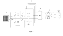
- a direct current side of a five-level inverter 10 is connected to a photovoltaic array 20 and configured to receive a PV input voltage at the direct current side.
- the PV input voltage is applied across a positive electrode of a capacitor C1 and a negative electrode of a capacitor C2, voltages of C1 and C2 relative to a middle point of DC-bus are V1Pos and V1Neg respectively.
- the PV input voltage is step up by two Boost circuits at the front of the five-level inverter 10, then is applied across a positive electrode of a bus capacitor C3 and a negative electrode of a bus capacitor C4, and voltages of C3 and C4 relative to the middle point of the DC-bus are V2Pos and V2Neg respectively.
- An output voltage from the grid side of the five-level inverter 10 is filtered by a filter 30, step up by a transformer 40 and then transmitted to a power grid.
- the five-level inverter 10 alternately outputs levels +V1Pos, -V1Neg, +V2Pos, -V2Neg and a zero level corresponding to the middle point of the DC-bus.
- the modulation may include four modulation sections:
- a corresponding duty ratio command value Dcmd meets 1-Vx/V1Pos ⁇ Dcmd ⁇ 1; in a case that Vcmd is greater than 0 and approaches V1Pos from a value less than V1Pos, Dcmd is close to 1, thereby resulting in many narrow pulses; and in a case that Vx/V1Pos is less than the duty ratio Dthrs corresponding to the sum of narrow pulse time and dead-band time, in order to ensure that switching devices operate safely, these narrow pulses need to be deleted and Dcmd is clamped to 1.
- Vcmd is greater than 0 and approaches +V1Pos from a value greater than +V1Pos
- Vcmd is less than 0 and approaches -V1Neg from a value greater than -V1Neg
- Vcmd is less than 0 and approaches -V1Neg from a value less than -V1Neg
- Vcmd approaches 0 there are also many narrow pulses to be deleted.
- deleting of narrow pulses results in distortion of the phase bridge output voltage.
- a method for modulating a five-level inverter, a device for modulating a five-level inverter, and a photovoltaic system are provided according to the present disclosure, to reduce the number of narrow pulses generated during modulating of the five-level inverter, thereby reducing the impact on the distortion of the phase bridge output voltage of the five-level inverter due to deleting of the narrow pulses, and the safety operation of the switching devices is guaranteed at the same time.
- a method for modulating a five-level inverter which includes:
- Vthrs1 Dthrs*(V2Pos-V1Pos)
- Vthrs2 Dthrs*V1Pos
- Vthrs3 Dthrs*V1Neg
- Vthrs4 Dthrs*(V2Neg-V1Neg).
- a method for modulating a five-level inverter which includes:
- Vthrs1 Dthrs*(V2Pos-V1Pos)
- Vthrs2 Dthrs*V1Pos
- Vthrs3 Dthrs*V1Neg
- Vthrs4 Dthrs*(V2Neg-V1Neg)
- Vthrs5 Dthrs*V1Pos
- Vthrs6 Dthrs*V1Neg.
- a device for modulating a five-level inverter which includes:
- Vthrs1 Dthrs*(V2Pos-V1Pos)
- Vthrs2 Dthrs*V1Pos
- Vthrs3 Dthrs*V1Neg
- Vthrs4 Dthrs*(V2Neg-V1Neg).
- a device for modulating a five-level inverter which includes:
- Vthrs1 Dthrs*(V2Pos-V1Pos)
- Vthrs2 Dthrs*V1Pos
- Vthrs3 Dthrs*V1Neg
- Vthrs4 Dthrs*(V2Neg-V1Neg)
- Vthrs5 Dthrs*V1Pos
- Vthrs6 Dthrs*V1Neg.
- a photovoltaic system which includes a photovoltaic array, two Boost circuits, a five-level inverter, a filter and a transformer, where a direct current side of the five-level inverter is connected to the photovoltaic array, and the grid side of the five-level inverter is connected to the power grid via the filter and the transformer; and the photovoltaic system further includes a controller connected to the five-level inverter, and the controller is configured to: acquire a voltage command value Vcmd of the phase bridge of the five-level inverter; control a first switching device and a fourth switching device to be switched on alternately in a case that Vcmd ⁇ V1Pos+Vthrs1; control the first switching device and a third switching device to be switched on alternately in a case that V1Pos-Vthrs2 ⁇ Vcmd ⁇ V1Pos+Vthrs1; control the fourth switching device and the third switching device to be switched on alternately in a case that 0 ⁇
- a photovoltaic system which includes a photovoltaic array, two Boost circuits, a five-level inverter, a filter and a transformer, where a direct current side of the five-level inverter is connected to the photovoltaic array via the two Boost circuits, and a grid side of the five-level inverter is connected to a power grid via the filter and the transformer; and the photovoltaic system further includes a controller connected to the five-level inverter, and the controller is configured to: acquire a voltage command value Vcmd of a phase bridge of the five-level inverter; control a first switching device and a fourth switching device to be switched on alternately in a case that Vcmd ⁇ V1Pos+Vthrs1; control the first switching device and a third switching device to be switched on alternately in a case that V1Pos-Vthrs2 ⁇ Vcmd ⁇ V1Pos+Vthrs1; control the fourth switching device and the third switching device to be switched on on
- the output voltage level of the five-level inverter is switched cross levels according to the present disclosure rather than between adjacent levels, such that the duty ratio is far away from 0 or 1 rather than approaching 0 or 1, thereby preventing generating narrow pulses in a case that Vcmd approaches +V1Pos or -V1Neg.
- the narrow pulses are generated in a case that Vcmd approaches +V1Pos, -V1Neg or 0; and according to the present disclosure, the number of the narrow pulses generated during modulating of the five-level inverter is reduced significantly, thereby reducing the impact on the distortion of the phase bridge output voltage of the five-level inverter due to deleting of the narrow pulses, and the safety operation of the switching devices is guaranteed at the same time.
- a method for modulating a five-level inverter is disclosed, to reduce the number of narrow pulses generated during modulating of the five-level inverter, thereby reducing the impact on the distortion of the phase bridge output voltage of the five-level inverter due to deleting of the narrow pulses, and the safety operation of the switching devices is guaranteed at the same time.
- a five-level inverter 10 alternately outputs five voltage levels +1, -1, +2, -2 and 0 in different combinations of switching states of switching devices, and values of the five voltage levels are +V1Pos, -V1Neg, +V2Pos, -V2Neg and 0 respectively.
- S2Pos indicates a first switching device, the level +2 is outputted when the first switching device is switched on;
- S2Neg indicates a second switching device, the level -2 is outputted when the second switching device is switched on;
- SO indicates a third switching device, the level 0 is outputted when the third switching device is switched on;
- S1Pos indicates a fourth switching device, the level +1 is outputted when the fourth switching device is switched on;
- S1Neg indicates a fifth switching device, the level -1 is outputted when the fifth switching device is switched on.
- Dthrs indicates a duty ratio corresponding to the sum of narrow pulse time and dead-band time of the five-level inverter 10, which is a known constant.
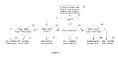
- the method for modulating a five-level inverter may include step S201 to step S212 hereinafter.
- step S201 a voltage command value Vcmd of a phase bridge of the five-level inverter is acquired.
- step 202 it is determined whether Vcmd ⁇ 0 is met; and if Vcmd ⁇ 0 is met, the method proceeds to step S203; otherwise, the method proceeds to step S205.
- step S203 it is determined whether Vcmd ⁇ V1Pos+Vthrs1 is met; and if Vcmd ⁇ V1Pos+Vthrs1 is met, the method proceeds to step S207; otherwise, the method proceeds to step S204, where Vthrs1 ⁇ Dthrs*(V2Pos-V1Pos).
- step S204 it is determined whether V1Pos-Vthrs2 ⁇ Vcmd ⁇ V1Pos+Vthrs1 is met; if V1Pos-Vthrs2 ⁇ Vcmd ⁇ V1Pos+Vthrs1 is met, the method proceeds to step 208; otherwise the method proceeds to step 209, where Vthrs2 ⁇ Dthrs*V1Pos.
- step S205 it is determined whether -V1Neg+Vthrs3 ⁇ Vcmd ⁇ 0 is met; and if -V1Neg+Vthrs3 ⁇ Vcmd ⁇ 0 is met, the method proceeds to step 210; otherwise, the method proceeds to step 206, where Vthrs3 ⁇ Dthrs*V1Neg.
- step 206 it is determined whether -V1Neg-Vthrs4 ⁇ Vcmd ⁇ -V1Neg+Vthrs3 is met; and if -V1Neg-Vthrs4 ⁇ Vcmd ⁇ -V1Neg+Vthrs3 is met, the method proceeds to step 211; otherwise, the method proceeds to step 212, where Vthrs4 ⁇ Dthrs*(V2Neg-V1Neg).
- step 207 a first modulation section is entered, in which the switching device S2Pos and the switching device S1Pos are controlled to be switched on alternately, and an output voltage level is switched between +V2Pos and +V1Pos.
- step 208 a second modulation section is entered, in which the switching device S2Pos and the switching device SO are controlled to be switched on alternately, and the output voltage level is switched between +V2Pos and 0.
- step 209 a third modulation section is entered, in which the switching device S1Pos and the switching device SO are controlled to be switched on alternately, and the output voltage level is switched between +V1Pos and 0.
- step 210 a fourth modulation section is entered, in which the switching device SO and the switching device S1Neg are controlled to be switched on alternately, and the output voltage level is switched between 0 and -V1Neg.
- step 211 a fifth modulation section is entered, in which the switching device SO and the switching device S2Neg are controlled to be switched on alternately, and the output voltage level is switched between 0 and -V2Neg.
- step 212 a sixth modulation section is entered, in which the switching device S1Neg and the switching device S2Neg are controlled to be switched on alternately, and the output voltage level is switched between -V1Neg and -V2Neg.
- duty ratio command values Dcmd for different modulation sections may be calculated based on the voltage command value Vcmd of each phase bridge (Vthrs1, Vthrs2, Vthrs3 and Vthrs4 are voltage thresholds for adjusting the modulation sections).
- Vcmd approaches -V1Neg
- the output voltage level of the five-level inverter is switched cross levels rather than between adjacent levels, such that the duty ratio is far way from 0 or 1 rather than approaching 0 or 1, thereby preventing generating narrow pulses in a case that Vcmd approaches +V1Pos or -V1Neg.
- the narrow pulses are generated only in a case that Vcmd approaches 0, the number of the narrow pulses is reduced greatly, thereby reducing the impact on the distortion of the phase bridge output voltage of the five-level inverter due to deleting of the narrow pulses, and the safety operation of the switching devices is guaranteed at the same time.
- FIG. 3 another method for modulating a five-level inverter is disclosed according to an embodiment of the present disclosure.
- the method may include step 301 to step 314 hereinafter.
- step 301 a voltage command value Vcmd of a phase bridge of the five-level inverter is acquired.
- step 302 it is determined whether Vcmd ⁇ Vthrs5 is met; and if Vcmd ⁇ Vthrs5 is met, the method proceeds to step 303; otherwise, the method proceeds to step 305.
- step 303 it is determined whether Vcmd ⁇ V1Pos+Vthrs1 is met; and if Vcmd ⁇ V1Pos+Vthrs1 is met, the method proceeds to step 308; otherwise, the method proceeds to step 304.
- step 304 it is determined whether V1Pos-Vthrs2 ⁇ Vcmd ⁇ V1Pos+Vthrs1 is met; and if V1Pos-Vthrs2 ⁇ Vcmd ⁇ V1Pos+Vthrs1 is met, the method proceeds to step 309; otherwise, the method proceeds to step 310.
- step 305 it is determined whether -Vthrs6 ⁇ Vcmd ⁇ Vthrs5 is met; and if -Vthrs6 ⁇ Vcmd ⁇ Vthrs5 is met, the method proceeds to step 311; otherwise, the method proceeds to step 306.
- step 306 it is determined whether -V1Neg+Vthrs3 ⁇ Vcmd ⁇ -Vthrs6 is met; and if -V1Neg+Vthrs3 ⁇ Vcmd ⁇ -Vthrs6 is met, the method proceeds to step 312; otherwise, the method proceeds to step 307.
- step 307 it is determined whether -V1Neg-Vthrs4 ⁇ Vcmd ⁇ -V1Neg+Vthrs3 is met; and if -V1Neg-Vthrs4 ⁇ Vcmd ⁇ -V1Neg+Vthrs3 is met, the method proceeds to step 313; otherwise, the method proceeds to step 314.
- step 308 a first modulation section is entered, in which the switching device S2Pos and the switching device S1Pos are controlled to be switched on alternately, and an output voltage level is switched between +V2Pos and +V1Pos.
- step 309 a second modulation section is entered, in which the switching device S2Pos and the switching device SO are controlled to be switched on alternately, and the output voltage level is switched between +V2Pos and 0.
- step 310 a third modulation section is entered, in which the switching device S1Pos and the switching device SO are controlled to be switched on alternately, and the output voltage level is switched between +V1Pos and 0.
- step 311 a fourth modulation section is entered, in which the switching device S1Pos and the switching device S1Neg are controlled to be switched on alternately, and the output voltage level is switched between +V1Pos and -V1Neg.
- step 312 a fifth modulation section is entered, in which the switching device SO and the switching device S1Neg are controlled to be switched on alternately, and the output voltage level is switched between 0 and -V1Neg.
- step 313 a sixth modulation section is entered, in which the switching device SO and the switching device S2Neg are controlled to be switched on alternately, and the output voltage level is switched between 0 and -V2Neg.
- step 314 a seventh modulation section is entered, in which the switching device S1Neg and the switching device S2Neg are controlled to be switched on alternately, and the output voltage level is switched between -V1Neg and -V2Neg.
- duty ratio command values Dcmd for different modulation sections may be calculated based on the voltage command value Vcmd of the phase bridge (Vthrs1, Vthrs2, Vthrs3, Vthrs4, Vthrs5 and Vthrs6 are voltage thresholds for adjusting the modulation sections).
- Vcmd approaches -V1Neg
- the output voltage level of the five-level inverter is switched cross levels rather than between adjacent levels, such that the duty ratio is far way from 0 or 1 rather than approaching 0 or 1, thereby preventing generating narrow pulses in a case that Vcmd approaches +V1Pos, -V1Neg or 0.
- the narrow pulses can be prevented from being generated both in a case that Vcmd approaches +V1Pos or -V1Neg and in a case that Vcmd approaches 0, thereby further reducing the impact on the distortion of the phase bridge output voltage of the five-level inverter due to deleting of the narrow pulses, and the safety operation of the switching devices is guaranteed at the same time.
- the modulation section to be entered is determined based on the value of Vcmd.
- the way for determining the modulation section to be entered based on Vcmd is not limited to the way disclosed above.
- a device for modulating a five-level inverter is further disclosed according to an embodiment of the present disclosure, to reduce the number of narrow pulses generated during modulating of the five-level inverter, thereby reducing the impact on the distortion of the phase bridge output voltage of the five-level inverter due to deleting of the narrow pulses, and the safety operation of the switching devices is guaranteed at the same time.
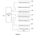
- the device includes an acquiring unit 401, a first processing unit 402, a second processing unit 403, a third processing unit 404, a fourth processing unit 405, a fifth processing unit 406 and a sixth processing unit 407.
- the acquiring unit 401 is configured to acquire a voltage command value Vcmd of a phase bridge of the five-level inverter.
- the first processing unit 402 is configured to control a switching device S2Pos and a switching device S1Pos to be switched on alternately in a case that Vcmd ⁇ V1Pos+Vthrs1.
- the second processing unit 403 is configured to control the switching device S2Pos and a switching device SO to be switched on alternately in a case that V1Pos-Vthrs2 ⁇ Vcmd ⁇ V1Pos+Vthrs1.
- the third processing unit 404 is configured to control the switching device S1Pos and the switching device SO to be switched on alternately in a case that 0 ⁇ Vcmd ⁇ V1Pos-Vthrs2.
- the fourth processing unit 405 is configured to control the switching device SO and a switching device S1Neg to be switched on alternately in a case that -V1Neg+Vthrs3 ⁇ Vcmd ⁇ 0.
- the fifth processing unit 406 is configured to control the switching device SO and a switching device S2Neg to be switched on alternately in a case that -V1Neg-Vthrs4 ⁇ Vcmd ⁇ -V1Neg+Vthrs3.
- the sixth processing unit 407 is configured to control the switching device S1Neg and the switching device S2Neg to be switched on alternately in a case that Vcmd ⁇ -V1Neg-Vthrs4.
- the device includes an acquiring unit 501, a first processing unit 502, a second processing unit 503, a third processing unit 504, a fourth processing unit 505, a fifth processing unit 506, a sixth processing unit 507 and a seventh processing unit 508.
- the acquiring unit 501 is configured to acquire a voltage command value Vcmd of a phase bridge of the five-level inverter.
- the first processing unit 502 is configured to control a switching device S2Pos and a switching device S1Pos to be switched on alternately in a case that Vcmd ⁇ V1Pos+Vthrs1.
- the second processing unit 503 is configured to control the switching device S2Pos and a switching device SO to be switched on alternately in a case that V1Pos-Vthrs2 ⁇ Vcmd ⁇ V1Pos+Vthrs1.
- the third processing unit 504 is configured to control the switching device S1Pos and the switching device SO to be switched on alternately in a case that Vthrs5 ⁇ Vcmd ⁇ V1Pos-Vthrs2.
- the fourth processing unit 505 is configured to control the switching device S1Pos and a switching device S1Neg to be switched on alternately in a case that -Vthrs6 ⁇ Vcmd ⁇ Vthrs5.
- the fifth processing unit 506 is configured to control the switching device SO and the switching device S1Neg to be switched on alternately in a case that -V1Neg+Vthrs3 ⁇ Vcmd ⁇ -Vthrs6.
- the sixth processing unit 507 is configured to control the switching device SO and a switching device S2Neg to be switched on alternately in a case that -V1Neg-Vthrs4 ⁇ Vcmd ⁇ -V1Neg+Vthrs3.
- the seventh processing unit 508 is configured to control the switching device S1Neg and the switching device S2Neg to be switched on alternately in a case that Vcmd ⁇ -V1Neg-Vthrs4.
- a photovoltaic system is further disclosed according to an embodiment of the present disclosure, to reduce the number of narrow pulses generated during modulating of a five-level inverter, thereby reducing the impact on the distortion of the phase bridge output voltage of the five-level inverter due to deleting of the narrow pulses, and the safety operation of the switching devices is guaranteed at the same time.
- the photovoltaic system includes a five-level inverter 10, a photovoltaic array 20, a filter 30, a transformer 40, two Boost circuits 50 and a controller 60.
- a direct current side of the five-level inverter 10 is connected to the photovoltaic array 20 via the two Boost circuits 50, and a grid side of the five-level inverter 10 is connected to a power grid via the filter 30 and the transformer 40.
- the controller 60 is connected to the five-level inverter 10 and configured to: acquire a voltage command value Vcmd of a phase bridge of the five-level inverter 10; control a switching device S2Pos and a switching device S1Pos to be switched on alternately in a case that Vcmd ⁇ V1Pos+Vthrs1; control the switching device S2Pos and a switching device SO to be switched on alternately in a case that V1Pos-Vthrs2 ⁇ Vcmd ⁇ V1Pos+Vthrs1; control the switching device S1Pos and the switching device SO to be switched on alternately in a case that 0 ⁇ Vcmd ⁇ V1Pos-Vthrs2; control the switching device SO and a switching device S1Neg to be switched on alternately in a case that -V1Neg+Vthrs3 ⁇ Vcmd ⁇ 0; control the switching device SO and a switching device S2Neg to be switched on alternately
- the photovoltaic system includes a five-level inverter, a photovoltaic array, a filter, a transformer, two Boost circuits and a controller.
- the embodiment differs from the above embodiment of the photovoltaic system in that: in the embodiment, the controller is connected to the five-level inverter and configured to: acquire a voltage command value Vcmd of a phase bridge of the five-level inverter; control a switching device S2Pos and a switching device S1Pos to be switched on alternately in a case that Vcmd ⁇ V1Pos+Vthrs1; control the switching device S2Pos and a switching device SO to be switched on alternately in a case that V1Pos-Vthrs2 ⁇ Vcmd ⁇ V1Pos+Vthrs1; control the switching device S1Pos and the switching device SO to be switched on alternately in a case that Vthrs5 ⁇ V
- the output voltage level of the five-level inverter is switched cross levels rather than between adjacent levels, such that the duty ratio is far away from 0 or 1 rather than approaching 0 or 1, thereby preventing generating narrow pulses in a case that Vcmd approaches +V1Pos or -V1Neg.
- the narrow pulses are generated in a case that Vcmd approaches +V1Pos, -V1Neg or 0; and according to the present disclosure, the number of the narrow pulses generated during modulating of the five-level inverter is reduced significantly, thereby reducing the impact on the distortion of the phase bridge output voltage of the five-level inverter due to deleting of the narrow pulses, and the safety operation of the switching devices is guaranteed at the same time.
Landscapes
- Engineering & Computer Science (AREA)
- Power Engineering (AREA)
- Inverter Devices (AREA)
Abstract
Description
- The present disclosure relates to the technical field of photovoltaic power generation, and in particular to a method for modulating a five-level inverter, a device for modulating a five-level inverter, and a photovoltaic system.
- As shown in
Figure 1 , a direct current side of a five-level inverter 10 is connected to aphotovoltaic array 20 and configured to receive a PV input voltage at the direct current side. The PV input voltage is applied across a positive electrode of a capacitor C1 and a negative electrode of a capacitor C2, voltages of C1 and C2 relative to a middle point of DC-bus are V1Pos and V1Neg respectively. And the PV input voltage is step up by two Boost circuits at the front of the five-level inverter 10, then is applied across a positive electrode of a bus capacitor C3 and a negative electrode of a bus capacitor C4, and voltages of C3 and C4 relative to the middle point of the DC-bus are V2Pos and V2Neg respectively. An output voltage from the grid side of the five-level inverter 10 is filtered by afilter 30, step up by atransformer 40 and then transmitted to a power grid. In different combinations of switching states of switching devices, the five-level inverter 10 alternately outputs levels +V1Pos, -V1Neg, +V2Pos, -V2Neg and a zero level corresponding to the middle point of the DC-bus. - In the conventional carrier based modulation method, based on the relationship between the voltage command value Vcmd of each phase bridge of the five-level inverter and the output voltage level, the modulation may include four modulation sections:
- 1) a first modulation section: in a case that Vcmd≥V1Pos, a switching device S2Pos and a switching device S1Pos are switched on alternately, and the output voltage level is switched between +V2Pos and +V1Pos;
- 2) a second modulation section: in a case that 0<Vcmd<VlPos, the switching device S1Pos and a switching device SO are switched on alternately, and the output voltage level is switched between +V1Pos and 0;
- 3) a third modulation section: in a case that -V1Neg≤Vcmd<0, the switching device SO and a switching device S1Neg are switched on alternately, and the output voltage level is switched between 0 and -V1Neg; and
- 4) a fourth modulation section: in a case that Vcmd<-V1Neg, the switching device S1Neg and a switching device S2Neg are switched on alternately, and the output voltage level is switched between -V1Neg and -V2Neg.
- However, in a case that V1Pos-Vx<Vcmd<V1Pos, a corresponding duty ratio command value Dcmd meets 1-Vx/V1Pos<Dcmd<1; in a case that Vcmd is greater than 0 and approaches V1Pos from a value less than V1Pos, Dcmd is close to 1, thereby resulting in many narrow pulses; and in a case that Vx/V1Pos is less than the duty ratio Dthrs corresponding to the sum of narrow pulse time and dead-band time, in order to ensure that switching devices operate safely, these narrow pulses need to be deleted and Dcmd is clamped to 1. Similarly, in a case that Vcmd is greater than 0 and approaches +V1Pos from a value greater than +V1Pos, Vcmd is less than 0 and approaches -V1Neg from a value greater than -V1Neg, Vcmd is less than 0 and approaches -V1Neg from a value less than -V1Neg, or Vcmd approaches 0, there are also many narrow pulses to be deleted. However, deleting of narrow pulses results in distortion of the phase bridge output voltage.
- In view of above, a method for modulating a five-level inverter, a device for modulating a five-level inverter, and a photovoltaic system are provided according to the present disclosure, to reduce the number of narrow pulses generated during modulating of the five-level inverter, thereby reducing the impact on the distortion of the phase bridge output voltage of the five-level inverter due to deleting of the narrow pulses, and the safety operation of the switching devices is guaranteed at the same time.
- A method for modulating a five-level inverter is provided, which includes:
- acquiring a voltage command value Vcmd of a phase bridge of the five-level inverter;
- controlling a first switching device and a fourth switching device to be switched on alternately in a case that Vcmd≥V1Pos+Vthrs1;
- controlling the first switching device and a third switching device to be switched on alternately in a case that V1Pos-Vthrs2≤Vcmd<V1Pos+Vthrs1;
- controlling the fourth switching device and the third switching device to be switched on alternately in a case that 0≤Vcmd<V1Pos-Vthrs2;
- controlling the third switching device and a fifth switching device to be switched on alternately in a case that -V1Neg+Vthrs3≤Vcmd<0;
- controlling the third switching device and a second switching device to be switched on alternately in a case that -V1Neg-Vthrs4≤Vcmd<-V1Neg+Vthrs3; and
- controlling the fifth switching device and the second switching device to be switched on alternately in a case that Vcmd<-V1Neg-Vthrs4,
- where Vthrs1≥Dthrs*(V2Pos-V1Pos), Vthrs2≥Dthrs*V1Pos, Vthrs3≥Dthrs*V1Neg, and Vthrs4≥Dthrs*(V2Neg-V1Neg); and Dthrs indicates the duty ratio corresponding to the sum of narrow pulse time and dead-band time of the five-level inverter; and
- the five-level inverter alternately outputs five voltage levels +1, -1, +2, -2 and 0 in different combinations of switching states of the switching devices, and values of the five voltage levels are +V1Pos, -V1Neg, +V2Pos, -V2Neg and 0 respectively; the level +1 is outputted when the fourth switching device is switched on; the level -1 is outputted when the fifth switching device is switched on; the level +2 is outputted when the first switching device is switched on; the level -2 is outputted when the second switching device is switched on; and the
level 0 is outputted when the third switching device is switched on. - Specifically, Vthrs1=Dthrs*(V2Pos-V1Pos), Vthrs2=Dthrs*V1Pos, Vthrs3=Dthrs*V1Neg and Vthrs4=Dthrs*(V2Neg-V1Neg).
- A method for modulating a five-level inverter is provided, which includes:
- acquiring a voltage command value Vcmd of a phase bridge of the five-level inverter;
- controlling the first switching device and the fourth switching device to be switched on alternately in a case that Vcmd≥V1Pos+Vthrs1;
- controlling the first switching device and a third switching device to be switched on alternately in a case that V1Pos-Vthrs2≤Vcmd<V1Pos+Vthrs1;
- controlling the fourth switching device and the third switching device to be switched on alternately in a case that Vthrs5≤Vcmd<V1Pos-Vthrs2;
- controlling the fourth switching device and a fifth switching device to be switched on alternately in a case that -Vthrs6≤Vcmd<Vthrs5;
- controlling the third switching device and the fifth switching device to be switched on alternately in a case that -V1Neg+Vthrs3≤Vcmd<-Vthrs6;
- controlling the third switching device and a second switching device to be switched on alternately in a case that -V1Neg-Vthrs4≤Vcmd<-V1Neg+Vthrs3; and
- controlling the fifth switching device and the second switching device to be switched on alternately in a case that Vcmd<-V1Neg-Vthrs4,
- where Vthrs1≥Dthrs*(V2Pos-V1Pos), Vthrs2≥Dthrs*V1Pos, Vthrs3≥Dthrs*V1Neg, Vthrs4≥Dthrs*(V2Neg-V1Neg), Vthrs5≥Dthrs*V1Pos and Vthrs6≥Dthrs*V1Neg; and Dthrs indicates a duty ratio corresponding to the sum of narrow pulse time and dead-band time of the five-level inverter; and
- the five-level inverter alternately outputs five voltage levels +1, -1, +2, -2 and 0 in different combinations of switching states of the switching devices, and values of the five voltage levels are +V1Pos, -V1Neg, +V2Pos, -V2Neg and 0 respectively; the level +1 is outputted when the fourth switching device is switched on; the level -1 is outputted when the fifth switching device is switched on; the level +2 is outputted when the first switching device is switched on; the level -2 is outputted when the second switching device is switched on; and the
level 0 is outputted when the third switching device is switched on. - Specifically, Vthrs1=Dthrs*(V2Pos-V1Pos), Vthrs2=Dthrs*V1Pos, Vthrs3=Dthrs*V1Neg, Vthrs4=Dthrs*(V2Neg-V1Neg), Vthrs5=Dthrs*V1Pos and Vthrs6=Dthrs*V1Neg.
- A device for modulating a five-level inverter is provided, which includes:
- an acquiring unit configured to acquire a voltage command value Vcmd of a phase bridge of the five-level inverter;
- a first processing unit configured to control a first switching device and a fourth switching device to be switched on alternately in a case that Vcmd≥V1Pos+Vthrs1;
- a second processing unit configured to control the first switching device and a third switching device to be switched on alternately in a case that V1Pos-Vthrs2≤Vcmd<V1Pos+Vthrs1;
- a third processing unit configured to control the fourth switching device and the third switching device to be switched on alternately in a case that 0≤Vcmd<V1Pos-Vthrs2;
- a fourth processing unit configured to control the third switching device and a fifth switching device to be switched on alternately in a case that -V1Neg+Vthrs3≤Vcmd<0;
- a fifth processing unit configured to control the third switching device and a second switching device to be switched on alternately in a case that -V1Neg-Vthrs4≤Vcmd<-V1Neg+Vthrs3; and
- a sixth processing unit configured to control the fifth switching device and the second switching device to be switched on alternately in a case that Vcmd<-V1Neg-Vthrs4,
- where Vthrs1≥Dthrs*(V2Pos-V1Pos), Vthrs2≥Dthrs*V1Pos, Vthrs3≥Dthrs*V1Neg and Vthrs4≥Dthrs*(V2Neg-V1Neg); and Dthrs indicates a duty ratio corresponding to the sum of narrow pulse time and dead-band time of the five-level inverter; and
- the five-level inverter alternately outputs five voltage levels +1, -1, +2, -2 and 0 in different combinations of switching states of the switching devices, and values of the five voltage levels are +V1Pos, -V1Neg, +V2Pos, -V2Neg and 0 respectively; the level +1 is outputted when the fourth switching device is switched on; the level -1 is outputted when the fifth switching device is switched on; the level +2 is outputted when the first switching device is switched on; the level -2 is outputted when the second switching device is switched on; and the
level 0 is outputted when the third switching device is switched on. - Specifically, Vthrs1=Dthrs*(V2Pos-V1Pos), Vthrs2=Dthrs*V1Pos, Vthrs3=Dthrs*V1Neg and Vthrs4=Dthrs*(V2Neg-V1Neg).
- A device for modulating a five-level inverter is provided, which includes:
- an acquiring unit configured to acquire a voltage command value Vcmd of a phase bridge of the five-level inverter;
- a first processing unit configured to control a first switching device and a fourth switching device to be switched on alternately in a case that Vcmd≥V1Pos+Vthrs1;
- a second processing unit configured to control the first switching device and a third switching device to be switched on alternately in a case that V1Pos-Vthrs2≤Vcmd<V1Pos+Vthrs1;
- a third processing unit configured to control the fourth switching device and the third switching device to be switched on alternately in a case that Vthrs5≤Vcmd<V1Pos-Vthrs2;
- a fourth processing unit configured to control the fourth switching device and a fifth switching device to be switched on alternately in a case that -Vthrs6≤Vcmd<Vthrs5;
- a fifth processing unit configured to control the third switching device and the fifth switching device to be switched on alternately in a case that -V1Neg+Vthrs3≤Vcmd<-Vthrs6;
- a sixth processing unit configured to control the third switching device and a second switching device to be switched on alternately in a case that -V1Neg-Vthrs4≤Vcmd<-V1Neg+Vthrs3; and
- a seventh processing unit configured to control the fifth switching device and the second switching device to be switched on alternately in a case that Vcmd<-V1Neg-Vthrs4,
- where Vthrs1≥Dthrs*(V2Pos-V1Pos), Vthrs2≥Dthrs*V1Pos, Vthrs3≥Dthrs*V1Neg, Vthrs4≥Dthrs*(V2Neg-V1Neg), Vthrs5≥Dthrs*V1Pos and Vthrs6≥Dthrs*V1Neg; and Dthrs indicates a duty ratio corresponding to the sum of narrow pulse time and dead-band time of the five-level inverter; and
- the five-level inverter alternately outputs five voltage levels +1, -1, +2, -2 and 0 in different combinations of switching states of the switching devices, and values of the five voltage levels are +V1Pos, -V1Neg, +V2Pos, -V2Neg and 0 respectively; the level +1 is outputted when the fourth switching device is switched on; the level -1 is outputted when the fifth switching device is switched on; the level +2 is outputted when the first switching device is switched on; the level -2 is outputted when the second switching device is switched on; and the
level 0 is outputted when the third switching device is switched on. - Specifically, Vthrs1=Dthrs*(V2Pos-V1Pos), Vthrs2=Dthrs*V1Pos, Vthrs3=Dthrs*V1Neg, Vthrs4=Dthrs*(V2Neg-V1Neg), Vthrs5=Dthrs*V1Pos and Vthrs6=Dthrs*V1Neg.
- A photovoltaic system is provided, which includes a photovoltaic array, two Boost circuits, a five-level inverter, a filter and a transformer, where a direct current side of the five-level inverter is connected to the photovoltaic array, and the grid side of the five-level inverter is connected to the power grid via the filter and the transformer; and
the photovoltaic system further includes a controller connected to the five-level inverter, and the controller is configured to: acquire a voltage command value Vcmd of the phase bridge of the five-level inverter; control a first switching device and a fourth switching device to be switched on alternately in a case that Vcmd≥V1Pos+Vthrs1; control the first switching device and a third switching device to be switched on alternately in a case that V1Pos-Vthrs2≤Vcmd<V1Pos+Vthrs1; control the fourth switching device and the third switching device to be switched on alternately in a case that 0≤Vcmd<V1Pos-Vthrs2; control the third switching device and a fifth switching device to be switched on alternately in a case that -V1Neg+Vthrs3≤Vcmd<0; control the third switching device and a second switching device to be switched on alternately in a case that -V1Neg-Vthrs4≤Vcmd<-V1Neg+Vthrs3; and control the fifth switching device and the second switching device to be switched on alternately in a case that Vcmd<-V1Neg-Vthrs4;
Vthrs1≥Dthrs*(V2Pos-V1Pos), Vthrs2≥Dthrs*V1Pos, Vthrs3≥Dthrs*V1Neg and Vthrs4≥Dthrs*(V2Neg-V1Neg); and Dthrs indicates a duty ratio corresponding to the sum of narrow pulse time and dead-band time of the five-level inverter; and
the five-level inverter alternately outputs five voltage levels +1, -1, +2, -2 and 0 in different combinations of switching states of the switching devices, and values of the five voltage levels are +V1Pos, -V1Neg, +V2Pos, -V2Neg and 0 respectively; the level +1 is outputted when the fourth switching device is switched on; the level -1 is outputted when the fifth switching device is switched on; the level +2 is outputted when the first switching device is switched on; the level -2 is outputted when the second switching device is switched on; and thelevel 0 is outputted when the third switching device is switched on. - A photovoltaic system is provided, which includes a photovoltaic array, two Boost circuits, a five-level inverter, a filter and a transformer, where a direct current side of the five-level inverter is connected to the photovoltaic array via the two Boost circuits, and a grid side of the five-level inverter is connected to a power grid via the filter and the transformer; and
the photovoltaic system further includes a controller connected to the five-level inverter, and the controller is configured to: acquire a voltage command value Vcmd of a phase bridge of the five-level inverter; control a first switching device and a fourth switching device to be switched on alternately in a case that Vcmd≥V1Pos+Vthrs1; control the first switching device and a third switching device to be switched on alternately in a case that V1Pos-Vthrs2≤Vcmd<V1Pos+Vthrs1; control the fourth switching device and the third switching device to be switched on alternately in a case that Vthrs5≤Vcmd<V1Pos-Vthrs2; control the fourth switching device and a fifth switching device to be switched on alternately in a case that -Vthrs6≤Vcmd<Vthrs5; control the third switching device and the fifth switching device to be switched on alternately in a case that -V1Neg+Vthrs3≤Vcmd<-Vthrs6; control the third switching device and a second switching device to be switched on alternately in a case that -V1Neg-Vthrs4≤Vcmd<-V1Neg+Vthrs3; and control the fifth switching device and the second switching device to be switched on alternately in a case that Vcmd<-V1Neg-Vthrs4;
Vthrs1≥Dthrs*(V2Pos-V1Pos), Vthrs2≥Dthrs*V1Pos, Vthrs3≥Dthrs*V1Neg, Vthrs4≥Dthrs*(V2Neg-V1Neg), Vthrs5≥Dthrs*V1Pos and Vthrs6≥Dthrs*V1Neg; and Dthrs indicates a duty ratio corresponding to the sum of narrow pulse time and dead-band time of the five-level inverter; and
the five-level inverter alternately outputs five voltage levels +1, -1, +2, -2 and 0 in different combinations of switching states of the switching devices, and values of the five voltage levels are +V1Pos, -V1Neg, +V2Pos, -V2Neg and 0 respectively; the level +1 is outputted when the fourth switching device is switched on; the level -1 is outputted when the fifth switching device is switched on; the level +2 is outputted when the first switching device is switched on; the level -2 is outputted when the second switching device is switched on; and thelevel 0 is outputted when the third switching device is switched on. - According to the above technical solutions, in a case that Vcmd approaches the output voltage level +V1Pos or -V1Neg, the output voltage level of the five-level inverter is switched cross levels according to the present disclosure rather than between adjacent levels, such that the duty ratio is far away from 0 or 1 rather than approaching 0 or 1, thereby preventing generating narrow pulses in a case that Vcmd approaches +V1Pos or -V1Neg. In the conventional technology, the narrow pulses are generated in a case that Vcmd approaches +V1Pos, -V1Neg or 0; and according to the present disclosure, the number of the narrow pulses generated during modulating of the five-level inverter is reduced significantly, thereby reducing the impact on the distortion of the phase bridge output voltage of the five-level inverter due to deleting of the narrow pulses, and the safety operation of the switching devices is guaranteed at the same time.
- In order to illustrate technical solutions in embodiments of the present disclosure or the conventional technology more clearly, hereinafter drawings to be used in the description of the embodiments or the conventional technology are introduced simply. Apparently, the drawings described below only describe the embodiments of the present disclosure. For those skilled in the art, other drawings may be obtained based on the provided drawings without any creative work.
-
Figure 1 is a schematic structural diagram of a photovoltaic system according to the conventional technology; -
Figure 2 is a flowchart of a method for modulating a five-level inverter according to an embodiment of the present disclosure; -
Figure 3 is a flowchart of another method for modulating a five-level inverter according to an embodiment of the present disclosure; -
Figure 4 is schematic structural diagram of a device for modulating a five-level inverter according to an embodiment of the present disclosure; -
Figure 5 is a schematic structural diagram of another device for modulating a five-level inverter according to an embodiment of the present disclosure; and -
Figure 6 is a schematic structural diagram of a photovoltaic system according to an embodiment of the present disclosure. - Hereinafter technical solutions of embodiments of the present disclosure are described clearly and completely in conjunction with the drawings of the embodiments of the present disclosure. Apparently, the described embodiments are only some of the embodiments of the present disclosure rather than all the embodiments. Any other embodiments obtained based on the embodiments of the present disclosure by those skilled in the art without any creative work fall within the protection scope of the present disclosure.
- According to embodiments of the present disclosure, a method for modulating a five-level inverter is disclosed, to reduce the number of narrow pulses generated during modulating of the five-level inverter, thereby reducing the impact on the distortion of the phase bridge output voltage of the five-level inverter due to deleting of the narrow pulses, and the safety operation of the switching devices is guaranteed at the same time. For facilitating describing, following definitions are made firstly.
- Referring to
Figure 1 , a five-level inverter 10 alternately outputs five voltage levels +1, -1, +2, -2 and 0 in different combinations of switching states of switching devices, and values of the five voltage levels are +V1Pos, -V1Neg, +V2Pos, -V2Neg and 0 respectively. For facilitating describing, S2Pos indicates a first switching device, the level +2 is outputted when the first switching device is switched on; S2Neg indicates a second switching device, the level -2 is outputted when the second switching device is switched on; SO indicates a third switching device, thelevel 0 is outputted when the third switching device is switched on; S1Pos indicates a fourth switching device, the level +1 is outputted when the fourth switching device is switched on; and S1Neg indicates a fifth switching device, the level -1 is outputted when the fifth switching device is switched on. Dthrs indicates a duty ratio corresponding to the sum of narrow pulse time and dead-band time of the five-level inverter 10, which is a known constant. - In conjunction with the above definitions, as shown in
Figure 2 , the method for modulating a five-level inverter may include step S201 to step S212 hereinafter. - In step S201, a voltage command value Vcmd of a phase bridge of the five-level inverter is acquired.
- In
step 202, it is determined whether Vcmd≥0 is met; and if Vcmd≥0 is met, the method proceeds to step S203; otherwise, the method proceeds to step S205. - In step S203, it is determined whether Vcmd≥V1Pos+Vthrs1 is met; and if Vcmd≥V1Pos+Vthrs1 is met, the method proceeds to step S207; otherwise, the method proceeds to step S204, where Vthrs1≥Dthrs*(V2Pos-V1Pos).
- In step S204, it is determined whether V1Pos-Vthrs2≤Vcmd<V1Pos+Vthrs1 is met; if V1Pos-Vthrs2≤Vcmd<V1Pos+Vthrs1 is met, the method proceeds to step 208; otherwise the method proceeds to step 209, where Vthrs2≥Dthrs*V1Pos.
- In step S205, it is determined whether -V1Neg+Vthrs3≤Vcmd<0 is met; and if -V1Neg+Vthrs3≤Vcmd<0 is met, the method proceeds to step 210; otherwise, the method proceeds to step 206, where Vthrs3≥Dthrs*V1Neg.
- In
step 206, it is determined whether -V1Neg-Vthrs4≤Vcmd<-V1Neg+Vthrs3 is met; and if -V1Neg-Vthrs4≤Vcmd<-V1Neg+Vthrs3 is met, the method proceeds to step 211; otherwise, the method proceeds to step 212, where Vthrs4≥Dthrs*(V2Neg-V1Neg). - In
step 207, a first modulation section is entered, in which the switching device S2Pos and the switching device S1Pos are controlled to be switched on alternately, and an output voltage level is switched between +V2Pos and +V1Pos. - In
step 208, a second modulation section is entered, in which the switching device S2Pos and the switching device SO are controlled to be switched on alternately, and the output voltage level is switched between +V2Pos and 0. - In
step 209, a third modulation section is entered, in which the switching device S1Pos and the switching device SO are controlled to be switched on alternately, and the output voltage level is switched between +V1Pos and 0. - In
step 210, a fourth modulation section is entered, in which the switching device SO and the switching device S1Neg are controlled to be switched on alternately, and the output voltage level is switched between 0 and -V1Neg. - In
step 211, a fifth modulation section is entered, in which the switching device SO and the switching device S2Neg are controlled to be switched on alternately, and the output voltage level is switched between 0 and -V2Neg. - In
step 212, a sixth modulation section is entered, in which the switching device S1Neg and the switching device S2Neg are controlled to be switched on alternately, and the output voltage level is switched between -V1Neg and -V2Neg. - Since a duty ratio is a ratio of the switch-on time of one of the two output voltage levels in each modulation section in a switching period to the whole switching period, duty ratio command values Dcmd for different modulation sections may be calculated based on the voltage command value Vcmd of each phase bridge (Vthrs1, Vthrs2, Vthrs3 and Vthrs4 are voltage thresholds for adjusting the modulation sections).
- 1) In the first modulation section, Dcmd=(Vcmd-V1Pos)/(V2Pos-V1Pos); and since Vcmd≥V1Pos+Vthrs1 is met in the first modulation section, Dcmd≥Vthrs1/(V2Pos-V1Pos).
In a case that Vcmd approaches +V1Pos, in order to prevent generating narrow pulses while the duty ratio approaches 0 in the first modulation section, Dcmd≥Vthrs1/(V2Pos-V1Pos)≥Dthrs needs to be met, and in this case Vthrs1≥Dthrs*(V2Pos-V1Pos). - 2) In the second modulation section, Dcmd=Vcmd/V2Pos, and since V1Pos-Vthrs2≤Vcmd<V1Pos+Vthrs1 is met in the second modulation section, (V1Pos-Vthrs2)/V2Pos≤Dcmd<(V1Pos+Vthrs1)/V2Pos.
In a normal operation case, in a case that Vcmd approaches +V1Pos, Dcmd is far away from 0 or 1, thereby preventing generating narrow pulses while the duty ratio approaches 0 or 1 in the second modulation section. - 3) In the third modulation section, Dcmd=Vcmd/V1Pos, and since 0≤Vcmd<V1Pos-Vthrs2 is met in the third modulation section, 0≤Dcmd<1-Vthrs2/V1Pos.
In a case that Vcmd approaches +V1Pos, in order to prevent generating narrow pulses while the duty ratio approaches 1 in the third modulation section, Dcmd<1-Vthrs2/V1Pos≤1-Dthrs needs to be met, and in this case Vthrs2≥Dthrs*V1Pos. - 4) In the fourth modulation section, Dcmd=-Vcmd/V1Neg, and since -V1Neg+Vthrs3≤Vcmd<0 is met in the fourth modulation section, 0<Dcmd≤1-Vthrs3/V1Neg.
In a case that Vcmd approaches -V1Neg, in order to prevent generating narrow pulses while the duty ratio approaches 1 in the fourth modulation section, Dcmd≤1-Vthrs3/V1Neg≤1-Dthrs needs to be met, and in this case Vthrs3≥Dthrs*V1Neg.
In the fifth modulation section, Dcmd=Vcmd/(-V2Neg), and since -V1Neg-Vthrs4≤Vcmd<-V1Neg+Vthrs3, (V1Neg-Vthrs3)/V2Neg<Dcmd≤(V1Neg+Vthrs4)/ V2Neg.
In a normal operation case, in a case that Vcmd approaches -V1Neg, Dcmd is far away from 0 or 1, thereby preventing generating narrow pulses while the duty ratio approaches 0 or 1 in the fifth modulation section. - 6) In the sixth modulation section, Dcmd=(Vcmd+V1Neg)/(-V2Neg+V1Neg), and since Vcmd<-V1Neg-Vthrs4 is met in the sixth modulation section, Dcmd>Vthrs4/(V2Neg-V1Neg).
- In a case that Vcmd approaches -V1Neg, in order to prevent generating narrow pulses while the duty ratio approaches 0 in the sixth modulation section, Dcmd>Vthrs4/(V2Neg-V1Neg)≥Dthrs needs to be met, and in this case Vthrs4≥Dthrs*(V2Neg-V1Neg).
- According to the above description, in the embodiment, in a case that Vcmd approaches the output voltage level +V1Pos or -V1Neg, the output voltage level of the five-level inverter is switched cross levels rather than between adjacent levels, such that the duty ratio is far way from 0 or 1 rather than approaching 0 or 1, thereby preventing generating narrow pulses in a case that Vcmd approaches +V1Pos or -V1Neg. In this case the narrow pulses are generated only in a case that Vcmd approaches 0, the number of the narrow pulses is reduced greatly, thereby reducing the impact on the distortion of the phase bridge output voltage of the five-level inverter due to deleting of the narrow pulses, and the safety operation of the switching devices is guaranteed at the same time.
- In view of that the output voltage being switched cross levels may increase switching losses, hence time for cross levels operation is expected to be as short as possible, i.e., values of Vthrs1, Vthrs2, Vthrs3 and Vthrs4 should be as small as possible. Therefore, Vthrs1, Vthrs2, Vthrs3 and Vthrs4 are calculated as follows to reduce the switching losses: Vthrs1=Dthrs*(V2Pos-V1Pos), Vthrs2=Dthrs*V1Pos, Vthrs3=Dthrs*V1Neg and Vthrs4=Dthrs*(V2Neg-V1Neg).
- In addition, referring to
Figure 3 , another method for modulating a five-level inverter is disclosed according to an embodiment of the present disclosure. The method may include step 301 to step 314 hereinafter. - In
step 301, a voltage command value Vcmd of a phase bridge of the five-level inverter is acquired. - In
step 302, it is determined whether Vcmd≥Vthrs5 is met; and if Vcmd≥Vthrs5 is met, the method proceeds to step 303; otherwise, the method proceeds to step 305. - In
step 303, it is determined whether Vcmd≥V1Pos+Vthrs1 is met; and if Vcmd≥V1Pos+Vthrs1 is met, the method proceeds to step 308; otherwise, the method proceeds to step 304. - In
step 304, it is determined whether V1Pos-Vthrs2≤Vcmd<V1Pos+Vthrs1 is met; and if V1Pos-Vthrs2≤Vcmd<V1Pos+Vthrs1 is met, the method proceeds to step 309; otherwise, the method proceeds to step 310. - In
step 305, it is determined whether -Vthrs6≤Vcmd<Vthrs5 is met; and if -Vthrs6≤Vcmd<Vthrs5 is met, the method proceeds to step 311; otherwise, the method proceeds to step 306. - In
step 306, it is determined whether -V1Neg+Vthrs3≤Vcmd<-Vthrs6 is met; and if -V1Neg+Vthrs3≤Vcmd<-Vthrs6 is met, the method proceeds to step 312; otherwise, the method proceeds to step 307. - In
step 307, it is determined whether -V1Neg-Vthrs4≤Vcmd<-V1Neg+Vthrs3 is met; and if -V1Neg-Vthrs4≤Vcmd<-V1Neg+Vthrs3 is met, the method proceeds to step 313; otherwise, the method proceeds to step 314. - In
step 308, a first modulation section is entered, in which the switching device S2Pos and the switching device S1Pos are controlled to be switched on alternately, and an output voltage level is switched between +V2Pos and +V1Pos. - In
step 309, a second modulation section is entered, in which the switching device S2Pos and the switching device SO are controlled to be switched on alternately, and the output voltage level is switched between +V2Pos and 0. - In
step 310, a third modulation section is entered, in which the switching device S1Pos and the switching device SO are controlled to be switched on alternately, and the output voltage level is switched between +V1Pos and 0. - In
step 311, a fourth modulation section is entered, in which the switching device S1Pos and the switching device S1Neg are controlled to be switched on alternately, and the output voltage level is switched between +V1Pos and -V1Neg. - In
step 312, a fifth modulation section is entered, in which the switching device SO and the switching device S1Neg are controlled to be switched on alternately, and the output voltage level is switched between 0 and -V1Neg. - In
step 313, a sixth modulation section is entered, in which the switching device SO and the switching device S2Neg are controlled to be switched on alternately, and the output voltage level is switched between 0 and -V2Neg. - In
step 314, a seventh modulation section is entered, in which the switching device S1Neg and the switching device S2Neg are controlled to be switched on alternately, and the output voltage level is switched between -V1Neg and -V2Neg. - Similar to the above embodiment of the method for modulating a five-level inverter, since a duty ratio is a ratio of the switch-on time of one of the two output voltage levels in each modulation section in a switching period to the whole switching period, duty ratio command values Dcmd for different modulation sections may be calculated based on the voltage command value Vcmd of the phase bridge (Vthrs1, Vthrs2, Vthrs3, Vthrs4, Vthrs5 and Vthrs6 are voltage thresholds for adjusting the modulation sections).
- 1) In the first modulation section, Dcmd=(Vcmd-V1Pos)/(V2Pos-V1Pos), and since Vcmd≥V1Pos+Vthrs1 is met in the first modulation section, Dcmd≥Vthrs1/(V2Pos-V1Pos).
In a case that Vcmd approaches +V1Pos, in order to prevent generating narrow pulses while the duty ratio approaches 0 in the first modulation section, Dcmd≥Vthrs1/(V2Pos-V1Pos)≥Dthrs needs to be met, and in this case Vthrs1≥Dthrs*(V2Pos-V1Pos). - 2) In the second modulation section, Dcmd=Vcmd/V2Pos, and since V1Pos-Vthrs2≤Vcmd<V1Pos+Vthrs1 is met in the second modulation section, (V1Pos-Vthrs2)/V2Pos≤Dcmd<(V1Pos+Vthrs1)/V2Pos.
In a normal operation case, in a case that Vcmd approaches +V1Pos, Dcmd is far away from 0 or 1, thereby preventing generating narrow pulses while the duty ratio approaches 0 or 1 in the second modulation section. - 3) In the third modulation section, Dcmd=Vcmd/V1Pos, and since Vthrs5≤Vcmd<V1Pos-Vthrs2 is met in the third modulation section, Vthrs5/V1Pos≤Dcmd<1-Vthrs2/V1Pos.
In a case that Vcmd approaches +V1Pos, in order to prevent generating narrow pulses while the duty ratio approaches 1 in the third modulation section, Dcmd<1-Vthrs2/V1Pos≤1-Dthrs needs to be met, and in this case Vthrs2≥Dthrs*V1Pos.
In a case that Vcmd approaches 0, in order to prevent generating narrow pulses while the duty ratio approaches 0 in the third modulation section, Dcmd≥Vthrs5/V1Pos≥Dthrs needs to be met, and in this case Vthrs5≥Dthrs*V1Pos. - 4) In the fourth modulation section, Dcmd=(Vcmd+V1Neg)/(V1Pos+V1Neg), and since -Vthrs6≤Vcmd<Vthrs5 is met in the fourth modulation section, (-Vthrs6+V1Neg)/(V1Pos+V1Neg)≤Dcmd<(Vthrs5+V1Neg)/(V1Pos+V1Neg).
In a normal operation case, in a case that Vcmd approaches 0, Dcmd is far away from 0 or 1, thereby preventing generating narrow pulses while the duty ratio approaches 0 or 1 in the fourth modulation section. - 5) In the fifth modulation section, Dcmd=-Vcmd/V1Neg, and since -V1Neg+Vthrs3≤Vcmd<-Vthrs6 is met in the fifth modulation section, Vthrs6/V1Neg<Dcmd≤1-Vthrs3/V1Neg.
In a case that Vcmd approaches -V1Neg, in order to prevent generating narrow pulses while the duty ratio approaches 1 in the fifth modulation section, Dcmd≤1-Vthrs3/V1Neg≤1-Dthrs needs to be met, and in this case Vthrs3≥Dthrs*V1Neg.
In a case that Vcmd approaches 0, in order to prevent generating narrow pulses while the duty ratio approaches 0 in the fifth modulation section, Dcmd>Vthrs6/V1Neg≥Dthrs needs to be met, and in this case Vthrs6≥Dthrs*V1Neg. - 6) In the sixth modulation section, Dcmd=Vcmd/(-V2Neg), and since -V1Neg-Vthrs4≤Vcmd<-V1Neg+Vthrs3, (V1Neg-Vthrs3)/V2Neg<Dcmd≤(V1Neg+Vthrs4)/ V2Neg.
In a normal operation case, in a case that Vcmd approaches -V1Neg, Dcmd is far away from 0 or 1, thereby preventing generating narrow pulses while the duty ratio approaches 0 or 1 in the fifth modulation section. - 7) In the seventh modulation section, Dcmd=(Vcmd+V1Neg)/(-V2Neg+V1Neg), and since Vcmd<-V1Neg-Vthrs4 is met in the seventh modulation section, Dcmd>Vthrs4/(V2Neg-V1Neg).
- In a case that Vcmd approaches -V1Neg, in order to prevent generating narrow pulses while the duty ratio approaches 0 in the seventh modulation section, Dcmd>Vthrs4/(V2Neg-V1Neg)≥Dthrs needs to be met, and in this case Vthrs4≥Dthrs*(V2Neg-V1Neg).
- According to the above description, in the embodiment, in a case that Vcmd approaches the output voltage level +V1Pos, -V1Neg or 0, the output voltage level of the five-level inverter is switched cross levels rather than between adjacent levels, such that the duty ratio is far way from 0 or 1 rather than approaching 0 or 1, thereby preventing generating narrow pulses in a case that Vcmd approaches +V1Pos, -V1Neg or 0. As compared with the above embodiment of the method for modulating a five-level inverter, in the embodiment, the narrow pulses can be prevented from being generated both in a case that Vcmd approaches +V1Pos or -V1Neg and in a case that Vcmd approaches 0, thereby further reducing the impact on the distortion of the phase bridge output voltage of the five-level inverter due to deleting of the narrow pulses, and the safety operation of the switching devices is guaranteed at the same time.
- Similarly, in view of that the output voltage level being switched cross levels may increase the switching losses, hence time for cross levels operation is expected to be as short as possible, i.e., values of Vthrs1 to Vthrs6 should be as small as possible. Therefore, Vthrs1 to Vthrs6 are calculated as follows to reduce the switching losses: Vthrs1=Dthrs*(V2Pos-V1Pos), Vthrs2=Dthrs*V1Pos, Vthrs3=Dthrs*V1Neg, Vthrs4=Dthrs*(V2Neg-V1Neg), Vthrs5=Dthrs*V1Pos and Vthrs6=Dthrs*V1Neg.
- Finally, it should be noted that, in the two method embodiments above, the modulation section to be entered is determined based on the value of Vcmd. The way for determining the modulation section to be entered based on Vcmd is not limited to the way disclosed above.
- Referring to
Figure 4 , a device for modulating a five-level inverter is further disclosed according to an embodiment of the present disclosure, to reduce the number of narrow pulses generated during modulating of the five-level inverter, thereby reducing the impact on the distortion of the phase bridge output voltage of the five-level inverter due to deleting of the narrow pulses, and the safety operation of the switching devices is guaranteed at the same time. The device includes an acquiringunit 401, afirst processing unit 402, asecond processing unit 403, athird processing unit 404, afourth processing unit 405, afifth processing unit 406 and asixth processing unit 407. - The acquiring
unit 401 is configured to acquire a voltage command value Vcmd of a phase bridge of the five-level inverter. - The
first processing unit 402 is configured to control a switching device S2Pos and a switching device S1Pos to be switched on alternately in a case that Vcmd≥V1Pos+Vthrs1. - The
second processing unit 403 is configured to control the switching device S2Pos and a switching device SO to be switched on alternately in a case that V1Pos-Vthrs2≤Vcmd<V1Pos+Vthrs1. - The
third processing unit 404 is configured to control the switching device S1Pos and the switching device SO to be switched on alternately in a case that 0≤Vcmd<V1Pos-Vthrs2. - The
fourth processing unit 405 is configured to control the switching device SO and a switching device S1Neg to be switched on alternately in a case that -V1Neg+Vthrs3≤Vcmd<0. - The
fifth processing unit 406 is configured to control the switching device SO and a switching device S2Neg to be switched on alternately in a case that -V1Neg-Vthrs4≤Vcmd<-V1Neg+Vthrs3. - And the
sixth processing unit 407 is configured to control the switching device S1Neg and the switching device S2Neg to be switched on alternately in a case that Vcmd<-V1Neg-Vthrs4. - Specifically, Vthrs1≥Dthrs*(V2Pos-V1Pos), Vthrs2≥Dthrs*V1Pos, Vthrs3≥Dthrs*V1Neg and Vthrs4≥Dthrs*(V2Neg-V1Neg).
- Preferably, Vthrs1 to Vthrs4 are calculated as follows: Vthrs1=Dthrs*(V2Pos-V1Pos), Vthrs2=Dthrs*V1Pos, Vthrs3=Dthrs*V1Neg and Vthrs4=Dthrs*(V2Neg-V1Neg).
- Referring to
Figure 5 , another device for modulating a five-level inverter is further disclosed according to an embodiment of the present disclosure. The device includes an acquiringunit 501, afirst processing unit 502, asecond processing unit 503, athird processing unit 504, afourth processing unit 505, afifth processing unit 506, asixth processing unit 507 and aseventh processing unit 508. - The acquiring
unit 501 is configured to acquire a voltage command value Vcmd of a phase bridge of the five-level inverter. - The
first processing unit 502 is configured to control a switching device S2Pos and a switching device S1Pos to be switched on alternately in a case that Vcmd≥V1Pos+Vthrs1. - The
second processing unit 503 is configured to control the switching device S2Pos and a switching device SO to be switched on alternately in a case that V1Pos-Vthrs2≤Vcmd<V1Pos+Vthrs1. - The
third processing unit 504 is configured to control the switching device S1Pos and the switching device SO to be switched on alternately in a case that Vthrs5≤Vcmd<V1Pos-Vthrs2. - The
fourth processing unit 505 is configured to control the switching device S1Pos and a switching device S1Neg to be switched on alternately in a case that -Vthrs6≤Vcmd<Vthrs5. - The
fifth processing unit 506 is configured to control the switching device SO and the switching device S1Neg to be switched on alternately in a case that -V1Neg+Vthrs3≤Vcmd<-Vthrs6. - The
sixth processing unit 507 is configured to control the switching device SO and a switching device S2Neg to be switched on alternately in a case that -V1Neg-Vthrs4≤Vcmd<-V1Neg+Vthrs3. - And the
seventh processing unit 508 is configured to control the switching device S1Neg and the switching device S2Neg to be switched on alternately in a case that Vcmd<-V1Neg-Vthrs4. - Specifically, Vthrs1≥Dthrs*(V2Pos-V1Pos), Vthrs2≥Dthrs*V1Pos, Vthrs3≥Dthrs*V1Neg, Vthrs4≥Dthrs*(V2Neg-V1Neg), Vthrs5≥Dthrs*V1Pos and Vthrs6≥Dthrs*V1Neg.
- Preferably, Vthrs1 to Vthrs6 are calculated as follows: Vthrs1=Dthrs*(V2Pos-V1Pos), Vthrs2=Dthrs*V1Pos, Vthrs3=Dthrs*V1Neg, Vthrs4=Dthrs*(V2Neg-V1Neg), Vthrs5=Dthrs*V1Pos and Vthrs6=Dthrs*V1Neg.
- In addition, referring to
Figure 6 , a photovoltaic system is further disclosed according to an embodiment of the present disclosure, to reduce the number of narrow pulses generated during modulating of a five-level inverter, thereby reducing the impact on the distortion of the phase bridge output voltage of the five-level inverter due to deleting of the narrow pulses, and the safety operation of the switching devices is guaranteed at the same time. The photovoltaic system includes a five-level inverter 10, aphotovoltaic array 20, afilter 30, atransformer 40, twoBoost circuits 50 and acontroller 60. - A direct current side of the five-
level inverter 10 is connected to thephotovoltaic array 20 via the twoBoost circuits 50, and a grid side of the five-level inverter 10 is connected to a power grid via thefilter 30 and thetransformer 40. - The
controller 60 is connected to the five-level inverter 10 and configured to: acquire a voltage command value Vcmd of a phase bridge of the five-level inverter 10; control a switching device S2Pos and a switching device S1Pos to be switched on alternately in a case that Vcmd≥V1Pos+Vthrs1; control the switching device S2Pos and a switching device SO to be switched on alternately in a case that V1Pos-Vthrs2≤Vcmd<V1Pos+Vthrs1; control the switching device S1Pos and the switching device SO to be switched on alternately in a case that 0≤Vcmd<V1Pos-Vthrs2; control the switching device SO and a switching device S1Neg to be switched on alternately in a case that -V1Neg+Vthrs3≤Vcmd<0; control the switching device SO and a switching device S2Neg to be switched on alternately in a case that -V1Neg-Vthrs4≤Vcmd<-V1Neg+Vthrs3; and control the switching device S1Neg and the switching device S2Neg to be switched on alternately in a case that Vcmd<-V1Neg-Vthrs4. - Alternatively, another photovoltaic system is disclosed according to an embodiment of the present disclosure. The photovoltaic system includes a five-level inverter, a photovoltaic array, a filter, a transformer, two Boost circuits and a controller. The embodiment differs from the above embodiment of the photovoltaic system in that: in the embodiment, the controller is connected to the five-level inverter and configured to: acquire a voltage command value Vcmd of a phase bridge of the five-level inverter; control a switching device S2Pos and a switching device S1Pos to be switched on alternately in a case that Vcmd≥V1Pos+Vthrs1; control the switching device S2Pos and a switching device SO to be switched on alternately in a case that V1Pos-Vthrs2≤Vcmd<V1Pos+Vthrs1; control the switching device S1Pos and the switching device SO to be switched on alternately in a case that Vthrs5≤Vcmd<V1Pos-Vthrs2; control the switching device S1Pos and a switching device S1Neg to be switched on alternately in a case that -Vthrs6≤Vcmd<Vthrs5; control the switching device SO and the switching device S1Neg to be switched on alternately in a case that -V1Neg+Vthrs3≤Vcmd<-Vthrs6; control the switching device SO and a switching device S2Neg to be switched on alternately in a case that -V1Neg-Vthrs4≤Vcmd<-V1Neg+Vthrs3; and control the switching device S1Neg and the switching device S2Neg to be switched on alternately in a case that Vcmd<-V1Neg-Vthrs4.
- In summary, in the embodiment, in a case that Vcmd approaches the output voltage level +V1Pos or -V1Neg, the output voltage level of the five-level inverter is switched cross levels rather than between adjacent levels, such that the duty ratio is far away from 0 or 1 rather than approaching 0 or 1, thereby preventing generating narrow pulses in a case that Vcmd approaches +V1Pos or -V1Neg. In the conventional technology, the narrow pulses are generated in a case that Vcmd approaches +V1Pos, -V1Neg or 0; and according to the present disclosure, the number of the narrow pulses generated during modulating of the five-level inverter is reduced significantly, thereby reducing the impact on the distortion of the phase bridge output voltage of the five-level inverter due to deleting of the narrow pulses, and the safety operation of the switching devices is guaranteed at the same time.
- Various embodiments of the specification are described in a progressive way, each embodiment lays emphasis on the difference from other embodiments, and for the same or similar parts between various embodiments, one may refer to the description of other embodiments. For the devices provided according to the embodiments, since the devices corresponds to the method provided according to the embodiments, the description of the devices is simple, the related part may be referred to the description of the method embodiment.
- According to the above illustration of the disclosed embodiments, those skilled in the art can implement or practice the present disclosure. Many changes to these embodiments are apparent for those skilled in the art, and general principles defined herein can be implemented in other embodiments without departing from the spirit or scope of the present disclosure. Hence, the present disclosure is not limited to the embodiments disclosed herein, but is to conform to the widest scope in accordance with the principles and novel features disclosed herein.
Claims (10)
- A method for modulating a five-level inverter, comprising:acquiring a voltage command value Vcmd of a phase bridge of the five-level inverter;controlling a first switching device and a fourth switching device to be switched on alternately in a case that Vcmd≥V1Pos+Vthrs1;controlling the first switching device and a third switching device to be switched on alternately in a case that V1Pos-Vthrs2≤Vcmd<V1Pos+Vthrs1;controlling the fourth switching device and the third switching device to be switched on alternately in a case that 0≤Vcmd<V1Pos-Vthrs2;controlling the third switching device and a fifth switching device to be switched on alternately in a case that -V1Neg+Vthrs3≤Vcmd<0;controlling the third switching device and a second switching device to be switched on alternately in a case that -V1Neg-Vthrs4≤Vcmd<-V1Neg+Vthrs3; andcontrolling the fifth switching device and the second switching device to be switched on alternately in a case that Vcmd<-V1Neg-Vthrs4,wherein Vthrs1≥Dthrs*(V2Pos-V1Pos), Vthrs2≥Dthrs*V1Pos, Vthrs3≥Dthrs*V1Neg and Vthrs4≥Dthrs*(V2Neg-V1Neg); and Dthrs indicates a duty ratio corresponding to the sum of narrow pulse time and dead-band time of the five-level inverter; andthe five-level inverter alternately outputs five voltage levels +1, -1, +2, -2 and 0 in different combinations of switching states of the switching devices, and values of the five voltage levels are +V1Pos, -V1Neg, +V2Pos, -V2Neg and 0 respectively; the level +1 is outputted when the fourth switching device is switched on; the level -1 is outputted when the fifth switching device is switched on; the level +2 is outputted when the first switching device is switched on; the level -2 is outputted when the second switching device is switched on; and the level 0 is outputted when the third switching device is switched on.
- The method according to claim 1, wherein Vthrs1=Dthrs*(V2Pos-V1Pos), Vthrs2=Dthrs*V1Pos, Vthrs3=Dthrs*V1Neg and Vthrs4=Dthrs*(V2Neg-V1Neg).
- A method for modulating a five-level inverter, comprising:acquiring a voltage command value Vcmd of a phase bridge of the five-level inverter;controlling a first switching device and a fourth switching device to be switched on alternately in a case that Vcmd≥V1Pos+Vthrs1;controlling the first switching device and a third switching device to be switched on alternately in a case that V1Pos-Vthrs2≤Vcmd<V1Pos+Vthrs1;controlling the fourth switching device and the third switching device to be switched on alternately in a case that Vthrs5≤Vcmd<V1Pos-Vthrs2;controlling the fourth switching device and a fifth switching device to be switched on alternately in a case that -Vthrs6≤Vcmd<Vthrs5;controlling the third switching device and the fifth switching device to be switched on alternately in a case that -V1Neg+Vthrs3≤Vcmd<-Vthrs6;controlling the third switching device and a second switching device to be switched on alternately in a case that -V1Neg-Vthrs4≤Vcmd<-V1Neg+Vthrs3; andcontrolling the fifth switching device and the second switching device to be switched on alternately in a case that Vcmd<-V1Neg-Vthrs4,wherein Vthrs1≥Dthrs*(V2Pos-V1Pos), Vthrs2≥Dthrs*V1Pos, Vthrs3≥Dthrs*V1Neg, Vthrs4≥Dthrs*(V2Neg-V1Neg), Vthrs5≥Dthrs*V1Pos and Vthrs6≥Dthrs*V1Neg; and Dthrs indicates a duty ratio corresponding to the sum of narrow pulse time and dead-band time of the five-level inverter; andthe five-level inverter alternately outputs five voltage levels +1, -1, +2, -2 and 0 in different combinations of switching states of the switching devices, and values of the five voltage levels are +V1Pos, -V1Neg, +V2Pos, -V2Neg and 0 respectively; the level +1 is outputted when the fourth switching device is switched on; the level -1 is outputted when the fifth switching device is switched on; the level +2 is outputted when the first switching device is switched on; the level -2 is outputted when the second switching device is switched on; and the level 0 is outputted when the third switching device is switched on.
- The method according to claim 3, wherein Vthrs1=Dthrs*(V2Pos-V1Pos), Vthrs2=Dthrs*V1Pos, Vthrs3=Dthrs*V1Neg, Vthrs4=Dthrs*(V2Neg-V1Neg), Vthrs5=Dthrs*V1Pos and Vthrs6=Dthrs*V1Neg.
- A device for modulating a five-level inverter, comprising:an acquiring unit configured to acquire a voltage command value Vcmd of a phase bridge of the five-level inverter;a first processing unit configured to control a first switching device and a fourth switching device to be switched on alternately in a case that Vcmd≥V1Pos+Vthrs1;a second processing unit configured to control the first switching device and a third switching device to be switched on alternately in a case that V1Pos-Vthrs2≤Vcmd<V1Pos+Vthrs1;a third processing unit configured to control the fourth switching device and the third switching device to be switched on alternately in a case that 0≤Vcmd<V1Pos-Vthrs2;a fourth processing unit configured to control the third switching device and a fifth switching device to be switched on alternately in a case that -V1Neg+Vthrs3≤Vcmd<0;a fifth processing unit configured to control the third switching device and a second switching device to be switched on alternately in a case that -V1Neg-Vthrs4≤Vcmd<-V1Neg+Vthrs3; anda sixth processing unit configured to control the fifth switching device and the second switching device to be switched on alternately in a case that Vcmd<-V1Neg-Vthrs4,wherein Vthrs1≥Dthrs*(V2Pos-V1Pos), Vthrs2≥Dthrs*V1Pos, Vthrs3≥Dthrs*V1Neg and Vthrs4≥Dthrs*(V2Neg-V1Neg); and Dthrs indicates a duty ratio corresponding to the sum of narrow pulse time and dead-band time of the five-level inverter; andthe five-level inverter alternately outputs five voltage levels +1, -1, +2, -2 and 0 in different combinations of switching states of the switching devices, and values of the five voltage levels are +V1Pos, -V1Neg, +V2Pos, -V2Neg and 0 respectively; the level +1 is outputted when the fourth switching device is switched on; the level -1 is outputted when the fifth switching device is switched on; the level +2 is outputted when the first switching device is switched on; the level -2 is outputted when the second switching device is switched on; and the level 0 is outputted when the third switching device is switched on.
- The device according to claim 5, wherein Vthrs1=Dthrs*(V2Pos-V1Pos), Vthrs2=Dthrs*V1Pos, Vthrs3=Dthrs*V1Neg and Vthrs4=Dthrs*(V2Neg-V1Neg).
- A device for modulating a five-level inverter, comprising:an acquiring unit configured to acquire a voltage command value Vcmd of a phase bridge of the five-level inverter;a first processing unit configured to control a first switching device and a fourth switching device to be switched on alternately in a case that Vcmd≥V1Pos+Vthrs1;a second processing unit configured to control the first switching device and a third switching device to be switched on alternately in a case that V1Pos-Vthrs2≤Vcmd<V1Pos+Vthrs1;a third processing unit configured to control the fourth switching device and the third switching device to be switched on alternately in a case that Vthrs5≤Vcmd<V1Pos-Vthrs2;a fourth processing unit configured to control the fourth switching device and a fifth switching device to be switched on alternately in a case that -Vthrs6≤Vcmd<Vthrs5;a fifth processing unit configured to control the third switching device and the fifth switching device to be switched on alternately in a case that -V1Neg+Vthrs3≤Vcmd<-Vthrs6;a sixth processing unit configured to control the third switching device and a second switching device to be switched on alternately in a case that -V1Neg-Vthrs4≤Vcmd<-V1Neg+Vthrs3; anda seventh processing unit configured to control the fifth switching device and the second switching device to be switched on alternately in a case that Vcmd<-V1Neg-Vthrs4,wherein Vthrs1≥Dthrs*(V2Pos-V1Pos), Vthrs2≥Dthrs*V1Pos, Vthrs3≥Dthrs*V1Neg, Vthrs4≥Dthrs*(V2Neg-V1Neg), Vthrs5≥Dthrs*V1Pos and Vthrs6≥Dthrs*V1Neg; and Dthrs indicates a duty ratio corresponding to the sum of narrow pulse time and dead-band time of the five-level inverter; andthe five-level inverter alternately outputs five voltage levels +1, -1, +2, -2 and 0 in different combinations of switching states of the switching devices, and values of the five voltage levels are +V1Pos, -V1Neg, +V2Pos, -V2Neg and 0 respectively; the level +1 is outputted when the fourth switching device is switched on; the level -1 is outputted when the fifth switching device is switched on; the level +2 is outputted when the first switching device is switched on; the level -2 is outputted when the second switching device is switched on; and the level 0 is outputted when the third switching device is switched on.
- The device according to claim 7, wherein Vthrs1=Dthrs*(V2Pos-V1Pos), Vthrs2=Dthrs*V1Pos, Vthrs3=Dthrs*V1Neg, Vthrs4=Dthrs*(V2Neg-V1Neg), Vthrs5=Dthrs*V1Pos and Vthrs6=Dthrs*V1Neg.
- A photovoltaic system, comprising: a photovoltaic array, two Boost circuits, a five-level inverter, a filter and a transformer, wherein a direct current side of the five-level inverter is connected to the photovoltaic array via the two Boost circuits, and a grid side of the five-level inverter is connected to a power grid via the filter and the transformer; and
the photovoltaic system further comprises a controller connected to the five-level inverter, and the controller is configured to: acquire a voltage command value Vcmd of a phase bridge of the five-level inverter; control a first switching device and a fourth switching device to be switched on alternately in a case that Vcmd≥V1Pos+Vthrs1; control the first switching device and a third switching device to be switched on alternately in a case that V1Pos-Vthrs2≤Vcmd<V1Pos+Vthrs1; control the fourth switching device and the third switching device to be switched on alternately in a case that 0≤Vcmd<V1Pos-Vthrs2; control the third switching device and a fifth switching device to be switched on alternately in a case that -V1Neg+Vthrs3≤Vcmd<0; control the third switching device and a second switching device to be switched on alternately in a case that -V1Neg-Vthrs4≤Vcmd<-V1Neg+Vthrs3; and control the fifth switching device and the second switching device to be switched on alternately in a case that Vcmd<-V1Neg-Vthrs4;
Vthrs1≥Dthrs*(V2Pos-V1Pos), Vthrs2≥Dthrs*V1Pos, Vthrs3≥Dthrs*V1Neg and Vthrs4≥Dthrs*(V2Neg-V1Neg); and Dthrs indicates a duty ratio corresponding to the sum of narrow pulse time and dead-band time of the five-level inverter; and
the five-level inverter alternately outputs five voltage levels +1, -1, +2, -2 and 0 in different combinations of switching states of the switching devices, and values of the five voltage levels are +V1Pos, -V1Neg, +V2Pos, -V2Neg and 0 respectively; the level +1 is outputted when the fourth switching device is switched; the level -1 is outputted when the fifth switching device is switched on; the level +2 is outputted when the first switching device is switched on; the level -2 is outputted when the second switching device is switched on; and the level 0 is outputted when the third switching device is switched on. - A photovoltaic system, comprising a photovoltaic array, two Boost circuits, a five-level inverter, a filter and a transformer, wherein a direct current side of the five-level inverter is connected to the photovoltaic array via the two Boost circuits, and a grid side of the five-level inverter is connected to a power grid via the filter and the transformer; and
the photovoltaic system further comprises a controller connected to the five-level inverter, and the controller is configured to: acquire a voltage command value Vcmd of a phase bridge of the five-level inverter; control a first switching device and a fourth switching device to be switched on alternately in a case that Vcmd≥V1Pos+Vthrs1; control the first switching device and a third switching device to be switched on alternately in a case that V1Pos-Vthrs2≤Vcmd<V1Pos+Vthrs1; control the fourth switching device and the third switching device to be switched on alternately in a case that Vthrs5≤Vcmd<V1Pos-Vthrs2; control the fourth switching device and a fifth switching device to be switched on alternately in a case that -Vthrs6≤Vcmd<Vthrs5; control the third switching device and the fifth switching device to be switched on alternately in a case that -V1Neg+Vthrs3≤Vcmd<-Vthrs6; control the third switching device and a second switching device to be switched on alternately in a case that -V1Neg-Vthrs4≤Vcmd<-V1Neg+Vthrs3; and control the fifth switching device and the second switching device to be switched on alternately in a case that Vcmd<-V1Neg-Vthrs4;
Vthrs1≥Dthrs*(V2Pos-V1Pos), Vthrs2≥Dthrs*V1Pos, Vthrs3≥Dthrs*V1Neg, Vthrs4≥Dthrs*(V2Neg-V1Neg), Vthrs5≥Dthrs*V1Pos and Vthrs6≥Dthrs*V1Neg; and Dthrs indicates a duty ratio corresponding to the sum of narrow pulse time and dead-band time of the five-level inverter; and
the five-level inverter alternately outputs five voltage levels +1, -1, +2, -2 and 0 in different combinations of switching states of the switching devices, and values of the five voltage levels are +V1Pos, -V1Neg, +V2Pos, -V2Neg and 0 respectively; the level +1 is outputted when the fourth switching device is switched on; the level -1 is outputted when the fifth switching device is switched on; the level +2 is outputted when the first switching device is switched on; the level -2 is outputted when the second switching device is switched on; and the level 0 is outputted when the third switching device is switched on.
Applications Claiming Priority (1)
| Application Number | Priority Date | Filing Date | Title |
|---|---|---|---|
| CN201410802612.2A CN104393778B (en) | 2014-12-18 | 2014-12-18 | Method and device for modulating five-level inverter and photovoltaic system |
Publications (2)
| Publication Number | Publication Date |
|---|---|
| EP3035510A2 true EP3035510A2 (en) | 2016-06-22 |
| EP3035510A3 EP3035510A3 (en) | 2016-08-03 |
Family
ID=52611628
Family Applications (1)
| Application Number | Title | Priority Date | Filing Date |
|---|---|---|---|
| EP15193963.4A Ceased EP3035510A3 (en) | 2014-12-18 | 2015-11-10 | Method and device for modulating a five-level inverter, and photovoltaic system |
Country Status (4)
| Country | Link |
|---|---|
| US (1) | US10044291B2 (en) |
| EP (1) | EP3035510A3 (en) |
| JP (1) | JP6197015B2 (en) |
| CN (1) | CN104393778B (en) |
Families Citing this family (5)
| Publication number | Priority date | Publication date | Assignee | Title |
|---|---|---|---|---|
| CN105207506B (en) * | 2014-06-25 | 2017-12-29 | 华为技术有限公司 | A kind of control method of inverter, device and system |
| CN104410307B (en) * | 2014-12-18 | 2017-01-18 | 阳光电源股份有限公司 | Working mode switching method and device for five-level inverter |
| US10536000B2 (en) * | 2016-02-10 | 2020-01-14 | Tabuchi Electric Co., Ltd. | Grid independent operation control unit, power conditioner, and grid independent operation control method |
| JP6962081B2 (en) * | 2017-09-06 | 2021-11-05 | 株式会社明電舎 | Multi-level power converter |
| CN111478613B (en) * | 2020-04-20 | 2021-07-27 | 上海正泰电源系统有限公司 | DSP implementation method for restraining inverter narrow pulse |
Family Cites Families (16)
| Publication number | Priority date | Publication date | Assignee | Title |
|---|---|---|---|---|
| CN101790827B (en) * | 2007-06-04 | 2013-06-12 | 可持续能源技术公司 | Prediction scheme for step wave power converter and inductive inverter topology |
| JP2010246267A (en) | 2009-04-06 | 2010-10-28 | Fuji Electric Systems Co Ltd | Five-level inverter |
| JP5734609B2 (en) | 2010-09-22 | 2015-06-17 | 株式会社ダイヘン | Inverter device and grid-connected inverter system provided with this inverter device |
| DE202010012993U1 (en) | 2010-11-25 | 2012-02-27 | Sma Solar Technology Ag | Multipoint inverter circuit |
| US20120218795A1 (en) * | 2011-02-28 | 2012-08-30 | Siemens Corporation | Pulse width modulated control for hybrid inverters |
| JP5682459B2 (en) * | 2011-06-07 | 2015-03-11 | 富士電機株式会社 | 5-level conversion circuit |
| TWI479794B (en) * | 2011-08-04 | 2015-04-01 | Ablerex Electonic Co Ltd | Fifth-order dc to ac power circuit |
| JP5899454B2 (en) | 2011-11-30 | 2016-04-06 | パナソニックIpマネジメント株式会社 | INVERTER DEVICE CONTROL METHOD AND INVERTER DEVICE |
| EP2624433A1 (en) * | 2012-02-03 | 2013-08-07 | ABB Research Ltd. | Non-isolated PV inverter system with ground current mitigation |
| US9413268B2 (en) * | 2012-05-10 | 2016-08-09 | Futurewei Technologies, Inc. | Multilevel inverter device and method |
| US9270168B2 (en) * | 2013-03-15 | 2016-02-23 | Hamilton Sundstrand Corporation | Electromagnetic interference (EMI) reduction in multi-level power converter |
| DE102013005277B3 (en) * | 2013-03-26 | 2014-07-03 | Platinum Gmbh | Inverter circuit for use as multi-level inverter for converting DC voltage into AC voltage, has several switching devices for selectively connecting or disconnecting potentials of intermediate circuit to output of inverter circuit |
| US9806637B2 (en) * | 2013-04-30 | 2017-10-31 | Futurewei Technologies, Inc. | Soft switching inverter device and method |
| CN103457502A (en) * | 2013-05-17 | 2013-12-18 | 湖南大学 | Novel five-level inverter seven-segment type SVPWM modulation method |
| CN103368433A (en) * | 2013-07-31 | 2013-10-23 | 华为技术有限公司 | Inverter and PWM (pulse width modulation) modulation method |
| US9325252B2 (en) * | 2014-01-13 | 2016-04-26 | Rockwell Automation Technologies, Inc. | Multilevel converter systems and sinusoidal pulse width modulation methods |
-
2014
- 2014-12-18 CN CN201410802612.2A patent/CN104393778B/en active Active
-
2015
- 2015-11-10 EP EP15193963.4A patent/EP3035510A3/en not_active Ceased
- 2015-11-11 US US14/938,192 patent/US10044291B2/en active Active
- 2015-11-19 JP JP2015226897A patent/JP6197015B2/en active Active
Non-Patent Citations (1)
| Title |
|---|
| None |
Also Published As
| Publication number | Publication date |
|---|---|
| CN104393778B (en) | 2017-01-18 |
| JP2016119831A (en) | 2016-06-30 |
| JP6197015B2 (en) | 2017-09-13 |
| US20160181945A1 (en) | 2016-06-23 |
| CN104393778A (en) | 2015-03-04 |
| US10044291B2 (en) | 2018-08-07 |
| EP3035510A3 (en) | 2016-08-03 |
Similar Documents
| Publication | Publication Date | Title |
|---|---|---|
| EP3035510A2 (en) | Method and device for modulating a five-level inverter, and photovoltaic system | |
| JP6600841B2 (en) | Cascade type photovoltaic grid-connected inverter, control method and control apparatus therefor | |
| US20220368227A1 (en) | Boost power conversion circuit, method, inverter, apparatus, and system | |
| JP4527767B2 (en) | Power converter | |
| US10038392B2 (en) | Inverter | |
| EP3742605A1 (en) | Method in inverter for suppressing common mode impulse current generated when switching on an alternating current switch and application device thereof | |
| EP3285350B1 (en) | Cascaded photovoltaic grid-connected inverter, control method and control device for the same | |
| KR101421017B1 (en) | Method for controlling electric current of multi-level inverter | |
| EP3485340A1 (en) | A control method for improving conversion efficiency of a multi-channel mppt inverter | |
| US9172311B2 (en) | Switching arrangement for inverter, and inverter | |
| CN103944148A (en) | T-type three-level inverter protecting method and device and inverter circuit | |
| EP3633843B1 (en) | Current converter and driving method therefor | |
| CN104242349A (en) | Photovoltaic system with potential induced degradation prevention function and photovoltaic inverter | |
| NZ744037A (en) | Power conversion system and power conversion device | |
| EP3035509B1 (en) | Method and device for switching operation mode of a five-level inverter | |
| US10116228B2 (en) | Converter and power conversion device manufactured using the same | |
| EP3258580B1 (en) | Device and method for protecting direct current source | |
| KR102132036B1 (en) | Power supply deivce and power supply deivce for arc machining | |
| EP3958452A1 (en) | Neutral-point-clamped three-level circuit and control method | |
| US10389292B1 (en) | DC bus regulation using rectifier and inverter | |
| CN110249497B (en) | Bus voltage adjusting method and related equipment | |
| EP2963762B1 (en) | Floating voltage suppression in a pv-inverter | |
| EP3160030A1 (en) | Power converter control device | |
| EP3926821A1 (en) | Component voltage limiting method and application device and system thereof | |
| CN110138185B (en) | Parallel current sharing control method for staggered full-bridge converter of alternating current power supply device |
Legal Events
| Date | Code | Title | Description |
|---|---|---|---|
| PUAI | Public reference made under article 153(3) epc to a published international application that has entered the european phase |
Free format text: ORIGINAL CODE: 0009012 |
|
| AK | Designated contracting states |
Kind code of ref document: A2 Designated state(s): AL AT BE BG CH CY CZ DE DK EE ES FI FR GB GR HR HU IE IS IT LI LT LU LV MC MK MT NL NO PL PT RO RS SE SI SK SM TR |
|
| AX | Request for extension of the european patent |
Extension state: BA ME |
|
| PUAL | Search report despatched |
Free format text: ORIGINAL CODE: 0009013 |
|
| AK | Designated contracting states |
Kind code of ref document: A3 Designated state(s): AL AT BE BG CH CY CZ DE DK EE ES FI FR GB GR HR HU IE IS IT LI LT LU LV MC MK MT NL NO PL PT RO RS SE SI SK SM TR |
|
| AX | Request for extension of the european patent |
Extension state: BA ME |
|
| RIC1 | Information provided on ipc code assigned before grant |
Ipc: H02M 7/487 20070101ALI20160630BHEP Ipc: H02M 3/00 20060101ALN20160630BHEP Ipc: H02M 1/12 20060101ALN20160630BHEP Ipc: H02M 1/00 20060101AFI20160630BHEP Ipc: H02M 7/5395 20060101ALI20160630BHEP |
|
| STAA | Information on the status of an ep patent application or granted ep patent |
Free format text: STATUS: REQUEST FOR EXAMINATION WAS MADE |
|
| 17P | Request for examination filed |
Effective date: 20170203 |
|
| RBV | Designated contracting states (corrected) |
Designated state(s): AL AT BE BG CH CY CZ DE DK EE ES FI FR GB GR HR HU IE IS IT LI LT LU LV MC MK MT NL NO PL PT RO RS SE SI SK SM TR |
|
| STAA | Information on the status of an ep patent application or granted ep patent |
Free format text: STATUS: EXAMINATION IS IN PROGRESS |
|
| 17Q | First examination report despatched |
Effective date: 20180712 |
|
| STAA | Information on the status of an ep patent application or granted ep patent |
Free format text: STATUS: EXAMINATION IS IN PROGRESS |
|
| STAA | Information on the status of an ep patent application or granted ep patent |
Free format text: STATUS: THE APPLICATION HAS BEEN REFUSED |
|
| 18R | Application refused |
Effective date: 20210207 |