EP3035174A1 - Touch panel and method of manufacturing the same - Google Patents
Touch panel and method of manufacturing the same Download PDFInfo
- Publication number
- EP3035174A1 EP3035174A1 EP15177764.6A EP15177764A EP3035174A1 EP 3035174 A1 EP3035174 A1 EP 3035174A1 EP 15177764 A EP15177764 A EP 15177764A EP 3035174 A1 EP3035174 A1 EP 3035174A1
- Authority
- EP
- European Patent Office
- Prior art keywords
- pattern
- sensing electrodes
- conductive pattern
- touch panel
- connector
- Prior art date
- Legal status (The legal status is an assumption and is not a legal conclusion. Google has not performed a legal analysis and makes no representation as to the accuracy of the status listed.)
- Granted
Links
Images




Classifications
-
- G—PHYSICS
- G06—COMPUTING OR CALCULATING; COUNTING
- G06F—ELECTRIC DIGITAL DATA PROCESSING
- G06F3/00—Input arrangements for transferring data to be processed into a form capable of being handled by the computer; Output arrangements for transferring data from processing unit to output unit, e.g. interface arrangements
- G06F3/01—Input arrangements or combined input and output arrangements for interaction between user and computer
- G06F3/03—Arrangements for converting the position or the displacement of a member into a coded form
- G06F3/041—Digitisers, e.g. for touch screens or touch pads, characterised by the transducing means
-
- G—PHYSICS
- G06—COMPUTING OR CALCULATING; COUNTING
- G06F—ELECTRIC DIGITAL DATA PROCESSING
- G06F3/00—Input arrangements for transferring data to be processed into a form capable of being handled by the computer; Output arrangements for transferring data from processing unit to output unit, e.g. interface arrangements
- G06F3/01—Input arrangements or combined input and output arrangements for interaction between user and computer
- G06F3/03—Arrangements for converting the position or the displacement of a member into a coded form
- G06F3/041—Digitisers, e.g. for touch screens or touch pads, characterised by the transducing means
- G06F3/044—Digitisers, e.g. for touch screens or touch pads, characterised by the transducing means by capacitive means
- G06F3/0443—Digitisers, e.g. for touch screens or touch pads, characterised by the transducing means by capacitive means using a single layer of sensing electrodes
-
- G—PHYSICS
- G06—COMPUTING OR CALCULATING; COUNTING
- G06F—ELECTRIC DIGITAL DATA PROCESSING
- G06F3/00—Input arrangements for transferring data to be processed into a form capable of being handled by the computer; Output arrangements for transferring data from processing unit to output unit, e.g. interface arrangements
- G06F3/01—Input arrangements or combined input and output arrangements for interaction between user and computer
- G06F3/03—Arrangements for converting the position or the displacement of a member into a coded form
- G06F3/041—Digitisers, e.g. for touch screens or touch pads, characterised by the transducing means
- G06F3/044—Digitisers, e.g. for touch screens or touch pads, characterised by the transducing means by capacitive means
- G06F3/0446—Digitisers, e.g. for touch screens or touch pads, characterised by the transducing means by capacitive means using a grid-like structure of electrodes in at least two directions, e.g. using row and column electrodes
-
- G—PHYSICS
- G06—COMPUTING OR CALCULATING; COUNTING
- G06F—ELECTRIC DIGITAL DATA PROCESSING
- G06F2203/00—Indexing scheme relating to G06F3/00 - G06F3/048
- G06F2203/041—Indexing scheme relating to G06F3/041 - G06F3/045
- G06F2203/04103—Manufacturing, i.e. details related to manufacturing processes specially suited for touch sensitive devices
-
- G—PHYSICS
- G06—COMPUTING OR CALCULATING; COUNTING
- G06F—ELECTRIC DIGITAL DATA PROCESSING
- G06F2203/00—Indexing scheme relating to G06F3/00 - G06F3/048
- G06F2203/041—Indexing scheme relating to G06F3/041 - G06F3/045
- G06F2203/04111—Cross over in capacitive digitiser, i.e. details of structures for connecting electrodes of the sensing pattern where the connections cross each other, e.g. bridge structures comprising an insulating layer, or vias through substrate
Definitions
- the present application relates to a touch panel and a method of manufacturing the same.
- Touch panels are being applied to liquid crystal displays (LCDs) or organic light-emitting displays as input devices.
- a touch panel is a device touched by a user's finger or an object such as a pen to input a command.
- the touch panel recognizes a touch position by sensing a change in capacitance or voltage between two electrodes and provides a user's command corresponding to the touch position to a display device.
- a touch panel includes two sensing electrodes for sensing a position touched by a finger or an object and wiring lines respectively connected to the two sensing electrodes. Therefore, to manufacture a touch panel, a mask for forming sensing electrodes and a mask for forming wiring lines are needed, and a photolithography process is performed using the masks.
- the photolithography process includes forming a photosensitive layer, exposing the photosensitive layer to light by using a mask, and developing the exposed photosensitive layer.
- one photolithography process includes a number of steps
- the addition of the photolithography process to the process of manufacturing a touch panel can complicate the entire manufacturing process, and contamination or defects can occur in the process of removing the photosensitive layer.
- aspects of the inventive concept provide a touch panel which can be manufactured in a simplified process and a method of manufacturing the touch panel.
- a touch panel includes: a substrate which includes a sensing area and a peripheral area; a plurality of first sensing electrodes which are located on a surface of the substrate and arranged along a first direction in the sensing area and a plurality of second sensing electrodes which are arranged along a second direction intersecting the first direction; a first connector which is located on the surface of the substrate and connects the first sensing electrodes along the first direction; an insulating layer pattern which is located on the first connector; a second connector which is located on the insulating layer pattern, intersects the first connector to be insulated from the first connector, and connects the second sensing electrodes along the second direction; a plurality of wiring lines which are located on the surface of the substrate, located in the peripheral area, and electrically connected to the first sensing electrodes or the second sensing electrodes; and a conductive pattern which is located between each of the second sensing electrodes and the second connector.
- a method of manufacturing a touch panel includes forming a first conductive layer on a surface of a substrate.
- a second conductive layer is formed on the first conductive layer.
- a plurality of first sensing electrodes which are arranged along a first direction are formed.
- a plurality of second sensing electrodes which are arranged along a second direction intersecting the first direction are formed.
- the first conductive layer and the second conductive layer are patterned to form a conductive pattern which is located on each of the first and second sensing electrodes, a first connector, and a plurality of wiring patterns which connect the first sensing electrodes along the first direction.
- An insulating layer pattern which covers the first connector is formed.
- a third conductive layer which covers the first sensing electrodes, the second sensing electrodes, the conductive pattern, the insulating layer pattern, and the wiring patterns, is formed on the surface of the substrate.
- a fourth conductive layer is formed on the third conductive layer.
- a second connector and a plurality of wiring lines which intersect the first connector and connect the second sensing electrodes along the second direction are formed by patterning the third conductive layer, the fourth conductive layer, and the conductive pattern.
- the touch panel 10 includes a substrate 100, a plurality of sensing electrodes 200, a first connector 220, a conductive pattern 233, an insulating layer pattern 240, a second connector 250, and a plurality of wiring lines (270, 280).
- the sensing electrodes 200, the first connector 220, the conductive pattern 233, the insulating layer pattern 240, the second connector 250, and the wiring lines (270, 280) are disposed on a surface of the substrate 100.
- the substrate 100 may be made of a transparent material.
- the transparent material may be, but is not limited to, tempered glass, acrylic resin, polyethylene terephthalate (PET), polycarbonate (PC), polyimide (PI), polyethersulfone (PES), polymethly methacrylate (PMMA), polyethylene naphthalate (PEN), metal foil, fiber reinforced plastic (FRP), or silicon rubber.
- the substrate 100 may have rigidity. However, the inventive concept is not limited thereto, and the substrate 100 may also have ductility. In other words, the substrate 100 may be a flexible substrate.
- the substrate 100 may include a sensing area AA and a peripheral area NA defined outside the sensing area AA.
- the sensing area AA is an area for sensing a touch position of a hand or an object.
- the sensing electrodes 200, the first connector 220, the conductive pattern 233, the insulating layer pattern 240, and the second connector 250 may be located on the surface of the substrate 100 in the sensing area AA.
- the peripheral area NA is located outside the sensing area AA.
- the wiring lines (270, 280) connected to the sensing electrodes 200 and a pad unit 290 connected to the wiring lines (270, 280) may be located on the surface of the substrate 100 in the peripheral area NA.
- a driver circuit board (not illustrated) for driving the touch panel 10 may be electrically connected to the pad unit 290.
- the sensing electrodes 200 may be located on the surface of the substrate 100 in the sensing area AA.
- the sensing electrodes 200 may include a plurality of first sensing electrodes 210 arranged in a first direction (a vertical direction in the drawings) and a plurality of second sensing electrodes 230 arranged in a second direction (a horizontal direction in the drawings) intersecting the first direction.
- the first sensing electrodes 210 and the second sensing electrodes 230 may be separated from each other.
- the first sensing electrodes 210 and the second sensing electrodes 230 may be physically separated from each other and may not directly contact each other.
- the first sensing electrodes 210 and the second sensing electrodes 230 may be electrically insulated from each other.
- the first sensing electrodes 210 and the second sensing electrodes 230 may be located at the same level. When the first and second sensing electrodes 210 and 230 are located at the same level, it means that they are located on the same layer. In some embodiments, the first sensing electrodes 210 and the second sensing electrodes 230 may be formed on the surface of the substrate 100 to directly contact the substrate 100.
- the first sensing electrodes 210 and the second sensing electrodes 230 may be made of an optically transparent light-transmitting conductive material.
- the optically transparent conductive material denotes not only a conductive material that is transparent but also a conductive material that is opaque but is perceived as transparent when seen with the naked eye because basic constituent units of the conductive material are very small and arranged at an appropriate density.
- the light-transmitting conductive material may be a metal material.
- the light-transmitting conductive material may be metal nanowires, and the metal nanowires may be nanowires that contain silver (Ag).
- the inventive concept is not limited thereto, and the metal nanowires may also contain gold (Au), platinum (Pt), nickel (Ni), or silicon.
- the first sensing electrodes 210 and the second sensing electrodes 230 may be formed of the same material in the same process.
- the first sensing electrodes 210 neighboring each other along the first direction may be connected by the first connector 220 located on the surface of the substrate 100.
- the first connector 220 may be located on the surface of the substrate 100 in the sensing area AA.
- the first connector 220 may include a lower conductive pattern 221 located on the surface of the substrate 100 and an upper conductive pattern 223 located on the lower conductive pattern 221.
- the lower conductive pattern 221 may be located at the same level as the first sensing electrodes 210 and the second sensing electrodes 230.
- the lower conductive pattern 221 may be formed on the surface of the substrate 100 to directly contact the substrate 100.
- the lower conductive pattern 221 may be made of a light-transmitting conductive material.
- the light-transmitting conductive material may be a metal material.
- the light-transmitting conductive material may be metal nanowires.
- the metal nanowires are the same as those described above in the description of the first sensing electrodes 210 and the second sensing electrodes 230, and thus a detailed description thereof is omitted.
- the lower conductive pattern 221 may be made of the same material as the first sensing electrodes 210 and the second sensing electrodes 230 and may be formed in the same process as the first sensing electrodes 210 and the second sensing electrodes 230. In addition, the lower conductive pattern 221 may be formed integrally with each of the first sensing electrodes 210.
- the upper conductive pattern 223 may be made of a transparent conductive material.
- the transparent conductive material may be a zinc oxide-based material.
- the zinc oxide-based material may include, but not limited to, at least one of indium zinc oxide (IZO), Al-doped zinc oxide (AZO), and gallium zinc oxide (GZO).
- the upper conductive pattern 223 may be made of the same material as the conductive patterns 233 and a first wiring pattern 271 which will be described later.
- the lower conductive pattern 221 and the upper conductive pattern 223 may have substantially the same planar shape. More specifically, when seen in plan view, the lower conductive pattern 221 and the upper conductive pattern 223 may have the same planar shape and completely overlap each other.
- the insulating layer pattern 240 may be located on the first connector 220 to cover the first connector 220.
- the insulating layer pattern 240 may completely cover the first connector 220.
- at least part of the insulating layer pattern 240 may extend onto each of the second sensing electrodes 230. In other words, at least part of the insulating layer pattern 240 may partially cover an upper portion of each of the second sensing electrodes 230.
- the insulating layer pattern 240 may be made of an insulating material.
- the insulating material may be an organic insulating material.
- the organic insulating material may be positive photosensitive resin.
- the positive photosensitive resin may include, but is not limited to, binder resin exemplified by alkali-soluble resin, a photosensitizer having various structures, and a solvent.
- the second connector 250 may be located on the insulating layer pattern 240 and intersect the first connector 220 to be insulated from the first connector 220.
- the second connector 250 may electrically connect the second sensing electrodes 230 neighboring each other along the second direction (or the horizontal direction in FIG. 2 ).
- the second connector 250 may be made of a conductive material and may have a multilayer structure.
- the second connector 250 may include a first conductive pattern 251 located on each of the second sensing electrodes 230 and the insulating layer pattern 240 and a second conductive pattern 253 located on the first conductive pattern 251.
- the first conductive pattern 251 may be located on the insulating layer pattern 240 and directly contact the insulating layer pattern 240.
- the first conductive pattern 251 may extend onto each of the second sensing electrodes 230 to electrically connect the second sensing electrodes 230 neighboring each other along the second direction.
- the first conductive pattern 251 may contain a conductive material with low resistivity.
- the conductive material with low resistivity may have a lower resistance value than the first sensing electrodes 210 and the second sensing electrodes 230.
- the conductive material with low resistivity may be molybdenum (Mo), silver (Ag), titanium (Ti), copper (Cu), aluminum (Al), or Mo/Al/Mo.
- the conductive material with low resistivity may be, but is not limited to, copper (Cu).
- the first conductive pattern 251 may be made of the same material as a third wiring pattern 281 which will be described later.
- the second conductive pattern 253 may be located on the first conductive pattern 251 and may function as a capping layer that protects the first conductive pattern 251.
- the second conductive pattern 253 may be made of a transparent conductive material.
- the transparent conductive material may be a zinc oxide-based material.
- the zinc oxide-based material may include, but not limited to, at least one of IZO, AZO, and GZO.
- the second conductive pattern 253 may be made of the same material as a fourth wiring pattern 283 which will be described later.
- the second conductive pattern 253 may be made of the same material as the conductive pattern 233 which will be described later.
- the first conductive pattern 251 and the second conductive pattern 253 may have substantially the same planar shape. More specifically, when seen in plan view, the first conductive pattern 251 and the second conductive pattern 253 may have the same planar shape and completely overlap each other.
- the conductive pattern 233 may be located on each of the second sensing electrodes 230.
- the conductive pattern 233 may be located between each of the second sensing electrodes 230 and the second connector 250.
- part of the conductive pattern 233 may be located between each of the second sensing electrodes 230 and the insulating layer pattern 240.
- the conductive pattern 233 may be located only in an area OA, sometimes called an overlap area OA, in which each of the second sensing electrodes 230 overlaps the second connector 250. In other words, the conductive pattern 233 may not be located on an area NOA, sometimes called a non-overlap area NOA, of each of the second sensing electrodes 230 which is not overlapped by the second connector 250 and may not be located on each of the first sensing electrodes 210 on which the second connector 250 is not located.
- the conductive pattern 233 may directly contact the second connector 250 in a contact area CA in which the second connector 250 is electrically connected to each of the second sensing electrodes 230.
- An outer side surface 233a of the conductive pattern 233 may substantially be continuous with an outer side surface 251a and 253a of the second connector 250.
- outer side surfaces of two elements are continuous with each other, there may be substantially no step difference between the two elements when seen in cross-sectional view.
- the outer side surface 233a of the conductive pattern 233 and the outer surface 251a and 253a of the second connector 250 may lie on the same virtual straight line when seen in cross-sectional view.
- the conductive pattern 233 may be made of a transparent conductive material.
- the transparent conductive material may be a zinc oxide-based material.
- the zinc oxide-based material may include, but not limited to, at least one of IZO, AZO, and GZO.
- the conductive pattern 233 may be made of the same material as the upper conductive pattern 223.
- the conductive pattern 233 may be made of the same material as a second wiring pattern 273.
- the conductive pattern 233 may also be made of the same material as the second conductive pattern 253 described above and the fourth wiring pattern 283 to be described later.
- the wiring lines (270, 280) may be located on the surface of the substrate 100 in the peripheral area NA.
- the wiring lines (270, 280) may be electrically connected to the first sensing electrodes 210 and the second sensing electrodes 230.
- each of the wiring lines (270, 280) may be directly connected to at least any one of the sensing electrodes 200 which is located at an outermost edge of the sensing area AA.
- Each of the wiring lines (270, 280) may include an inner wiring pattern 270 which is located on the substrate 100 and an outer wiring pattern 280 which covers the inner wiring pattern 270.
- the inner wiring pattern 270 may include the first wiring pattern 271 located on the substrate 100 and the second wiring pattern 273 located on the first wiring pattern 271.
- the first wiring pattern 271 may be may be made of an optically transparent light-transmitting conductive material.
- the light-transmitting conductive material may be a metal material.
- the light-transmitting conductive material may be metal nanowires, and the metal nanowires may be nanowires that contain Ag.
- the inventive concept is not limited thereto, and the metal nanowires may also contain Au, Pt, Ni, or silicon.
- the first wiring pattern 271 may be made of the same material as the first sensing electrodes 210 and the second sensing electrodes 230.
- the first wiring pattern 271 may be located at the same level as the first sensing electrodes 210 and the second sensing electrodes 230.
- the second wiring pattern 273 may be located on the first wiring pattern 271.
- the second wiring pattern 273 may be made of a transparent conductive material.
- the transparent conductive material may be a zinc oxide-based material.
- the zinc oxide-based material may include, but not limited to, at least one of IZO, AZO, and GZO.
- the second wiring pattern 273 may be made of the same material as the conductive pattern 233 and the upper conductive pattern 223 described above.
- the first wiring pattern 271 and the second wiring pattern 273 may have substantially the same planar shape. More specifically, when seen in plan view, the first wiring pattern 271 and the second wiring pattern 273 may have the same planar shape and completely overlap each other.
- the outer wiring pattern 280 may be located on the inner wiring pattern 270 and extend onto the surface of the substrate 100 over the inner wiring pattern 270.
- the outer wiring pattern 280 may include the third wiring pattern 281 and the fourth wiring pattern 283 located on the third wiring pattern 281.
- the third wiring pattern 281 may contain a conductive material with low resistivity.
- the conductive material with low resistivity may be Mo, Ag, Ti, Cu, Al, or Mo/Al/Mo.
- the conductive material with low resistivity may be Cu.
- the third wiring pattern 281 may be made of the same material as the first wiring pattern 251 described above.
- the fourth wiring pattern 283 may be located on the third wiring pattern 281.
- the fourth wiring pattern 283 may be made of a transparent conductive material.
- the transparent conductive material may be a zinc oxide-based material.
- the zinc oxide-based material may include, but not limited to, at least one of IZO, AZO, and GZO.
- the fourth wiring pattern 283 may be made of the same material as the second conductive pattern 253 described above. In some embodiments, the fourth wiring pattern 283 may also be made of the same material as the conductive pattern 233 and the upper conductive pattern 223.
- a side surface 281a of the third wiring pattern 281 may be substantially continuous with a side surface 283a of the fourth wiring pattern 283. In other words, there may be substantially no step difference between the side surface 281a of the third wiring pattern 281 and the side surface 283a of the fourth wiring pattern 283.
- FIGS. 7 to 17 are cross-sectional views illustrating a method of manufacturing a touch panel according to an embodiment, more specifically, cross-sectional views taken along the line III-III' of FIG. 2 to describe steps of a method of manufacturing a touch panel according to an embodiment.
- a first conductive layer 51 and a second conductive layer 53 are sequentially stacked on a surface of a substrate 100 having a sensing area AA and a peripheral area NA defined, as illustrated in FIG. 7 .
- the material that forms the first conductive layer 51 is substantially the same as the material that forms the first sensing electrodes 210 and the second sensing electrodes 230 described above with reference to FIGS. 1 to 6 .
- the material that forms the second conductive layer 53 is substantially the same as the material that forms the conductive pattern 233 described above with reference to FIGS. 1 to 6 .
- a photosensitive layer 55 is formed on the second conductive layer 53.
- the photosensitive layer 55 may be formed by coating liquid photoresist or may be formed of dry film photoresist (DFR).
- the photosensitive layer 55 may be a positive photosensitive layer whose exposed portions can be removed by development.
- the inventive concept is not limited thereto, and the photosensitive layer 55 may also be a negative photosensitive layer whose unexposed portions can be removed by development.
- a case where the photosensitive layer 55 is of a positive type will be described below as an example.
- the first mask M1 may include a first light-blocking mask pattern P1 corresponding to an inner wiring pattern 270 (see FIGS. 1 to 6 ), a second light-blocking mask pattern P2 corresponding to a first connector 220 (see FIGS. 1 to 6 ), and third light-blocking mask patterns P3 corresponding to first sensing electrodes 210 (see FIGS. 1 to 6 ) and second sensing electrodes 230 (see FIGS. 1 to 6 ).
- the photosensitive layer 55 is exposed to light L by irradiating the light L toward the substrate 100 from above the substrate 100.
- the light L may be ultraviolet light (UV).
- portions corresponding to the first light-blocking mask pattern P1, the second light-blocking mask pattern P2 and the third light-blocking mask patterns P3 are not exposed to the light L, and the other portions are exposed to the light L.
- the exposed portions of the photosensitive layer 55 are removed by a development process.
- third portions 553 corresponding to the first sensing electrodes 210 (see FIGS. 1 to 6 ) and the second sensing electrodes 230 (see FIGS. 1 to 6 ) remain on the second conductive layer 53 as illustrated in FIG. 9 .
- the second conductive layer 53 and the first conductive layer 51 are successively etched using the remaining portions (i.e., the first portion 551, the second portion 552 and the third portions 553) of the photosensitive layer 55 as a mask.
- the inner wiring pattern 270, the first sensing electrodes 210 (see FIGS. 1 to 6 ), the first connector 220, the second sensing electrodes 230, and a conductive pattern 233' are formed.
- the first connector 220 may be structured to include a lower conductive pattern 221 and an upper conductive pattern 223 located on the lower conductive pattern 221.
- the inner wiring pattern 270 may be structured to include a first wiring pattern 271 and a second wiring pattern 273 located on the first wiring pattern 271.
- the remaining portions (i.e., the first portion 551, the second portion 552 and the third portions 553) of the photosensitive layer 55 are then removed.
- a photosensitive insulating layer 57 is formed on the surface of the substrate 100 to cover the inner wiring pattern 270, the first sensing electrodes 210 (see FIGS. 1 to 6 ), the first connector 220, the second sensing electrodes 230, and the conductive pattern 233'.
- the photosensitive insulating layer 57 may be an organic insulating material. In some embodiments, the photosensitive insulating layer 57 may be positive photosensitive resin.
- the second mask M2 may include a fourth light-blocking mask pattern P4 corresponding to an insulating layer pattern 240 (see FIGS. 1 to 6 ).
- the photosensitive insulating layer 57 is exposed to light L by irradiating the light L toward the substrate 100 from above the substrate 100. Then, an exposed portion of the photosensitive insulating layer 57 is removed.
- the insulating layer pattern 240 (see FIGS. 1 to 6 ) is formed to cover the first connector 220 as illustrated in FIG. 12 .
- the insulating layer pattern 240 may extend onto part of each of the second sensing electrodes 230. In this case, since the conductive pattern 233' is formed before the insulating layer pattern 240, part of the conductive pattern 233' may be located between each of the second sensing electrodes 230 and the insulating layer pattern 240.
- a third conductive layer 59 and a fourth conductive layer 61 are sequentially stacked on the surface of the substrate 100 to cover the inner wiring pattern 270, the first sensing electrodes 210 (see FIGS. 1 to 6 ), the first connector 220, the second sensing electrodes 230, the conductive pattern 233' and the insulating layer pattern 240.
- the material that forms the third conductive layer 59 is substantially the same as the material that forms the first conductive pattern 251 or the third wiring pattern 281 described above with reference to FIGS. 1 to 6 .
- the material that forms the fourth conductive layer 61 is substantially the same as the material that forms the second conductive pattern 253 or the fourth wiring pattern 283 described above with reference to FIGS. 1 to 6 .
- a photosensitive layer 63 is formed on the fourth conductive layer 61.
- the photosensitive layer 63 may be formed by coating liquid photoresist or may be formed of DFR.
- the photosensitive layer 63 may be a positive photosensitive layer.
- the inventive concept is not limited thereto, and the photosensitive layer 63 may also be a negative photosensitive layer.
- the photosensitive layer 63 is of a positive type will be described below as an example.
- the third mask M3 may include a fifth light-blocking mask pattern P5 corresponding to an outer wiring pattern 280 (see FIGS. 1 to 6 ) and a sixth light-blocking mask pattern P6 corresponding to a second connector 250 (see FIGS. 1 to 6 ).
- the photosensitive layer 63 is exposed to light L by irradiating the light L toward the substrate 100 from above the substrate 100.
- portions corresponding to the fifth light-blocking mask pattern P5 and the sixth light-blocking mask pattern P6 are not exposed to the light L, and the other portions are exposed to the light L.
- the exposed portions of the photosensitive layer 63 are removed by a development process. As a result, a fourth portion 631 corresponding to the outer wiring pattern 280 (see FIGS. 1 to 6 ) and a fifth portion 633 corresponding to the second connector 250 (see FIGS. 1 to 6 ) and a fifth portion 633 corresponding to the second connector 250 (see FIGS. 1 to 6 ) and a fifth portion 633 corresponding to the second connector 250 (see
- FIGS. 1 to 6 remain on the fourth conductive layer 61.
- the second connector 250 may be structured to include a first conductive pattern 251 and a second conductive pattern 253 located on the first conductive pattern 251.
- the outer wiring pattern 280 may be structured to include a third wiring pattern 281 and a fourth wiring pattern 283 located on the third wiring pattern 281.
- FIG. 17 The touch panel illustrated in FIG. 17 is the same as the touch panel 10 described above with reference to FIGS. 1 to 6 , and thus a detailed description thereof is omitted.
- wiring lines, first sensing electrodes, second sensing electrodes, a first connector, an insulating layer pattern, and a second connector can be formed using three masks. Therefore, the number of masks used in a manufacturing process can be reduced, thereby simplifying the manufacturing process.
- a conductive pattern is located on each of the first and second sensing electrodes.
- the conductive pattern can prevent the possible damage to the first sensing electrodes and the second sensing electrodes during the process of manufacturing a touch panel.
- the first sensing electrodes and the second sensing electrodes if made of metal nanowires, are more easily damaged during the manufacturing process.
- the damage to the first sensing electrodes and the second sensing electrodes can be prevented even if the first sensing electrodes and the second sensing electrodes are made of metal nanowires.
- the conductive pattern located on each of the first sensing electrodes and the second sensing electrodes can be etched in the process of forming the second connector. Therefore, a mask used to remove the conductive pattern can be omitted.
- a method of manufacturing a touch panel in a more simplified process and a touch panel manufactured using the method can be provided.
Landscapes
- Engineering & Computer Science (AREA)
- General Engineering & Computer Science (AREA)
- Theoretical Computer Science (AREA)
- Human Computer Interaction (AREA)
- Physics & Mathematics (AREA)
- General Physics & Mathematics (AREA)
- Position Input By Displaying (AREA)
- Laminated Bodies (AREA)
Description
- The present application relates to a touch panel and a method of manufacturing the same.
- Touch panels are being applied to liquid crystal displays (LCDs) or organic light-emitting displays as input devices. A touch panel is a device touched by a user's finger or an object such as a pen to input a command. The touch panel recognizes a touch position by sensing a change in capacitance or voltage between two electrodes and provides a user's command corresponding to the touch position to a display device.
- Generally, a touch panel includes two sensing electrodes for sensing a position touched by a finger or an object and wiring lines respectively connected to the two sensing electrodes. Therefore, to manufacture a touch panel, a mask for forming sensing electrodes and a mask for forming wiring lines are needed, and a photolithography process is performed using the masks.
- The photolithography process includes forming a photosensitive layer, exposing the photosensitive layer to light by using a mask, and developing the exposed photosensitive layer.
- Since one photolithography process includes a number of steps, the addition of the photolithography process to the process of manufacturing a touch panel can complicate the entire manufacturing process, and contamination or defects can occur in the process of removing the photosensitive layer.
- Aspects of the inventive concept provide a touch panel which can be manufactured in a simplified process and a method of manufacturing the touch panel.
- However, aspects of the inventive concept are not restricted to the ones set forth herein. The above and other aspects of the inventive concept will become more apparent to one of ordinary skill in the art to which the present application pertains by referencing the detailed description of the inventive concept given below.
- According to an aspect of the inventive concept, there is provided a touch panel. The touch panel includes: a substrate which includes a sensing area and a peripheral area; a plurality of first sensing electrodes which are located on a surface of the substrate and arranged along a first direction in the sensing area and a plurality of second sensing electrodes which are arranged along a second direction intersecting the first direction; a first connector which is located on the surface of the substrate and connects the first sensing electrodes along the first direction; an insulating layer pattern which is located on the first connector; a second connector which is located on the insulating layer pattern, intersects the first connector to be insulated from the first connector, and connects the second sensing electrodes along the second direction; a plurality of wiring lines which are located on the surface of the substrate, located in the peripheral area, and electrically connected to the first sensing electrodes or the second sensing electrodes; and a conductive pattern which is located between each of the second sensing electrodes and the second connector.
- According to another aspect of the inventive concept, there is provided a method of manufacturing a touch panel. The method includes forming a first conductive layer on a surface of a substrate. A second conductive layer is formed on the first conductive layer. A plurality of first sensing electrodes which are arranged along a first direction are formed. A plurality of second sensing electrodes which are arranged along a second direction intersecting the first direction are formed. The first conductive layer and the second conductive layer are patterned to form a conductive pattern which is located on each of the first and second sensing electrodes, a first connector, and a plurality of wiring patterns which connect the first sensing electrodes along the first direction. An insulating layer pattern which covers the first connector is formed. A third conductive layer, which covers the first sensing electrodes, the second sensing electrodes, the conductive pattern, the insulating layer pattern, and the wiring patterns, is formed on the surface of the substrate. A fourth conductive layer is formed on the third conductive layer. A second connector and a plurality of wiring lines which intersect the first connector and connect the second sensing electrodes along the second direction are formed by patterning the third conductive layer, the fourth conductive layer, and the conductive pattern.
- Other features and exemplary embodiments will be apparent from the following detailed description, the drawings, and the claims.
- The above and other aspects and features of the inventive concept will become more apparent by describing in detail exemplary embodiments thereof with reference to the attached drawings, in which:
-
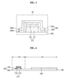
FIG. 1 is a schematic plan view of a touch panel according to an exemplary embodiment; -
FIG. 2 is an enlarged plan view of a portion P ofFIG. 1 ; -
FIG. 3 is a cross-sectional view of the touch panel taken along the line III-III' ofFIG. 2 ; -
FIGS. 4 and5 are enlarged views of portions X1, X2 ofFIG. 3 , respectively; -
FIG. 6 is a cross-sectional view of the touch panel taken along the line VI-VI' ofFIG. 2 ; and -
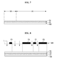
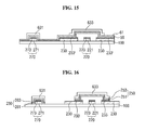
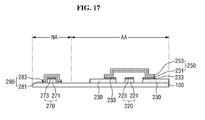
FIGS. 7, to 17 are cross-sectional views illustrating a method of manufacturing a touch panel according to an exemplary embodiment. - Referring to
FIGS. 1 to 6 , thetouch panel 10 according to the current embodiment includes asubstrate 100, a plurality ofsensing electrodes 200, afirst connector 220, aconductive pattern 233, aninsulating layer pattern 240, asecond connector 250, and a plurality of wiring lines (270, 280). - The
sensing electrodes 200, thefirst connector 220, theconductive pattern 233, theinsulating layer pattern 240, thesecond connector 250, and the wiring lines (270, 280) are disposed on a surface of thesubstrate 100. Thesubstrate 100 may be made of a transparent material. In some embodiments, the transparent material may be, but is not limited to, tempered glass, acrylic resin, polyethylene terephthalate (PET), polycarbonate (PC), polyimide (PI), polyethersulfone (PES), polymethly methacrylate (PMMA), polyethylene naphthalate (PEN), metal foil, fiber reinforced plastic (FRP), or silicon rubber. Thesubstrate 100 may have rigidity. However, the inventive concept is not limited thereto, and thesubstrate 100 may also have ductility. In other words, thesubstrate 100 may be a flexible substrate. - The
substrate 100 may include a sensing area AA and a peripheral area NA defined outside the sensing area AA. The sensing area AA is an area for sensing a touch position of a hand or an object. Thesensing electrodes 200, thefirst connector 220, theconductive pattern 233, theinsulating layer pattern 240, and thesecond connector 250 may be located on the surface of thesubstrate 100 in the sensing area AA. - The peripheral area NA is located outside the sensing area AA. The wiring lines (270, 280) connected to the
sensing electrodes 200 and apad unit 290 connected to the wiring lines (270, 280) may be located on the surface of thesubstrate 100 in the peripheral area NA. - A driver circuit board (not illustrated) for driving the
touch panel 10 may be electrically connected to thepad unit 290. - The
sensing electrodes 200 may be located on the surface of thesubstrate 100 in the sensing area AA. Thesensing electrodes 200 may include a plurality offirst sensing electrodes 210 arranged in a first direction (a vertical direction in the drawings) and a plurality ofsecond sensing electrodes 230 arranged in a second direction (a horizontal direction in the drawings) intersecting the first direction. - The
first sensing electrodes 210 and thesecond sensing electrodes 230 may be separated from each other. For example, thefirst sensing electrodes 210 and thesecond sensing electrodes 230 may be physically separated from each other and may not directly contact each other. Further, thefirst sensing electrodes 210 and thesecond sensing electrodes 230 may be electrically insulated from each other. - The
first sensing electrodes 210 and thesecond sensing electrodes 230 may be located at the same level. When the first andsecond sensing electrodes first sensing electrodes 210 and thesecond sensing electrodes 230 may be formed on the surface of thesubstrate 100 to directly contact thesubstrate 100. - The
first sensing electrodes 210 and thesecond sensing electrodes 230 may be made of an optically transparent light-transmitting conductive material. Here, the optically transparent conductive material denotes not only a conductive material that is transparent but also a conductive material that is opaque but is perceived as transparent when seen with the naked eye because basic constituent units of the conductive material are very small and arranged at an appropriate density. In some embodiments, the light-transmitting conductive material may be a metal material. In an example, the light-transmitting conductive material may be metal nanowires, and the metal nanowires may be nanowires that contain silver (Ag). However, the inventive concept is not limited thereto, and the metal nanowires may also contain gold (Au), platinum (Pt), nickel (Ni), or silicon. - In some embodiments, the
first sensing electrodes 210 and thesecond sensing electrodes 230 may be formed of the same material in the same process. - The
first sensing electrodes 210 neighboring each other along the first direction (or the vertical direction in the drawings) may be connected by thefirst connector 220 located on the surface of thesubstrate 100. - The
first connector 220 may be located on the surface of thesubstrate 100 in the sensing area AA. Thefirst connector 220 may include a lowerconductive pattern 221 located on the surface of thesubstrate 100 and an upperconductive pattern 223 located on the lowerconductive pattern 221. - In some embodiments, the lower
conductive pattern 221 may be located at the same level as thefirst sensing electrodes 210 and thesecond sensing electrodes 230. The lowerconductive pattern 221 may be formed on the surface of thesubstrate 100 to directly contact thesubstrate 100. - Like the
first sensing electrodes 210 and thesecond sensing electrodes 230, the lowerconductive pattern 221 may be made of a light-transmitting conductive material. The light-transmitting conductive material may be a metal material. In an example, the light-transmitting conductive material may be metal nanowires. The metal nanowires are the same as those described above in the description of thefirst sensing electrodes 210 and thesecond sensing electrodes 230, and thus a detailed description thereof is omitted. - In some embodiments, the lower
conductive pattern 221 may be made of the same material as thefirst sensing electrodes 210 and thesecond sensing electrodes 230 and may be formed in the same process as thefirst sensing electrodes 210 and thesecond sensing electrodes 230. In addition, the lowerconductive pattern 221 may be formed integrally with each of thefirst sensing electrodes 210. - The upper
conductive pattern 223 may be made of a transparent conductive material. In some embodiments, the transparent conductive material may be a zinc oxide-based material. In an example, the zinc oxide-based material may include, but not limited to, at least one of indium zinc oxide (IZO), Al-doped zinc oxide (AZO), and gallium zinc oxide (GZO). The upperconductive pattern 223 may be made of the same material as theconductive patterns 233 and afirst wiring pattern 271 which will be described later. - The lower
conductive pattern 221 and the upperconductive pattern 223 may have substantially the same planar shape. More specifically, when seen in plan view, the lowerconductive pattern 221 and the upperconductive pattern 223 may have the same planar shape and completely overlap each other. - The insulating
layer pattern 240 may be located on thefirst connector 220 to cover thefirst connector 220. The insulatinglayer pattern 240 may completely cover thefirst connector 220. In some embodiments, at least part of the insulatinglayer pattern 240 may extend onto each of thesecond sensing electrodes 230. In other words, at least part of the insulatinglayer pattern 240 may partially cover an upper portion of each of thesecond sensing electrodes 230. - The insulating
layer pattern 240 may be made of an insulating material. In some embodiments, the insulating material may be an organic insulating material. In an exemplary embodiment, the organic insulating material may be positive photosensitive resin. The positive photosensitive resin may include, but is not limited to, binder resin exemplified by alkali-soluble resin, a photosensitizer having various structures, and a solvent. - The
second connector 250 may be located on the insulatinglayer pattern 240 and intersect thefirst connector 220 to be insulated from thefirst connector 220. Thesecond connector 250 may electrically connect thesecond sensing electrodes 230 neighboring each other along the second direction (or the horizontal direction inFIG. 2 ). - The
second connector 250 may be made of a conductive material and may have a multilayer structure. In an example, thesecond connector 250 may include a firstconductive pattern 251 located on each of thesecond sensing electrodes 230 and the insulatinglayer pattern 240 and a secondconductive pattern 253 located on the firstconductive pattern 251. - The first
conductive pattern 251 may be located on the insulatinglayer pattern 240 and directly contact the insulatinglayer pattern 240. The firstconductive pattern 251 may extend onto each of thesecond sensing electrodes 230 to electrically connect thesecond sensing electrodes 230 neighboring each other along the second direction. - In some embodiments, the first
conductive pattern 251 may contain a conductive material with low resistivity. The conductive material with low resistivity may have a lower resistance value than thefirst sensing electrodes 210 and thesecond sensing electrodes 230. In an example, the conductive material with low resistivity may be molybdenum (Mo), silver (Ag), titanium (Ti), copper (Cu), aluminum (Al), or Mo/Al/Mo. In a more specific embodiment, the conductive material with low resistivity may be, but is not limited to, copper (Cu). In some embodiments, the firstconductive pattern 251 may be made of the same material as athird wiring pattern 281 which will be described later. - The second
conductive pattern 253 may be located on the firstconductive pattern 251 and may function as a capping layer that protects the firstconductive pattern 251. In some embodiments, the secondconductive pattern 253 may be made of a transparent conductive material. In an exemplary embodiment, the transparent conductive material may be a zinc oxide-based material. The zinc oxide-based material may include, but not limited to, at least one of IZO, AZO, and GZO. The secondconductive pattern 253 may be made of the same material as afourth wiring pattern 283 which will be described later. In some embodiments, the secondconductive pattern 253 may be made of the same material as theconductive pattern 233 which will be described later. - The first
conductive pattern 251 and the secondconductive pattern 253 may have substantially the same planar shape. More specifically, when seen in plan view, the firstconductive pattern 251 and the secondconductive pattern 253 may have the same planar shape and completely overlap each other. - The
conductive pattern 233 may be located on each of thesecond sensing electrodes 230. Theconductive pattern 233 may be located between each of thesecond sensing electrodes 230 and thesecond connector 250. In addition, when part of the insulatinglayer pattern 240 is located on each of thesecond sensing electrodes 230, part of theconductive pattern 233 may be located between each of thesecond sensing electrodes 230 and the insulatinglayer pattern 240. - In some embodiments, the
conductive pattern 233 may be located only in an area OA, sometimes called an overlap area OA, in which each of thesecond sensing electrodes 230 overlaps thesecond connector 250. In other words, theconductive pattern 233 may not be located on an area NOA, sometimes called a non-overlap area NOA, of each of thesecond sensing electrodes 230 which is not overlapped by thesecond connector 250 and may not be located on each of thefirst sensing electrodes 210 on which thesecond connector 250 is not located. When part of the insulatinglayer pattern 240 is located on each of thesecond sensing electrodes 230, theconductive pattern 233 may directly contact thesecond connector 250 in a contact area CA in which thesecond connector 250 is electrically connected to each of thesecond sensing electrodes 230. - An
outer side surface 233a of theconductive pattern 233 may substantially be continuous with anouter side surface second connector 250. When outer side surfaces of two elements are continuous with each other, there may be substantially no step difference between the two elements when seen in cross-sectional view. For example, there may be substantially no step difference between theouter side surface 233a of theconductive pattern 233 and theouter side surface second connector 250. In other words, theouter side surface 233a of theconductive pattern 233 and theouter surface second connector 250 may lie on the same virtual straight line when seen in cross-sectional view. - The
conductive pattern 233 may be made of a transparent conductive material. In an exemplary embodiment, the transparent conductive material may be a zinc oxide-based material. The zinc oxide-based material may include, but not limited to, at least one of IZO, AZO, and GZO. As described above, theconductive pattern 233 may be made of the same material as the upperconductive pattern 223. In addition, theconductive pattern 233 may be made of the same material as asecond wiring pattern 273. In some embodiments, theconductive pattern 233 may also be made of the same material as the secondconductive pattern 253 described above and thefourth wiring pattern 283 to be described later. - The wiring lines (270, 280) may be located on the surface of the
substrate 100 in the peripheral area NA. The wiring lines (270, 280) may be electrically connected to thefirst sensing electrodes 210 and thesecond sensing electrodes 230. In some embodiments, each of the wiring lines (270, 280) may be directly connected to at least any one of thesensing electrodes 200 which is located at an outermost edge of the sensing area AA. - Each of the wiring lines (270, 280) may include an
inner wiring pattern 270 which is located on thesubstrate 100 and anouter wiring pattern 280 which covers theinner wiring pattern 270. - The
inner wiring pattern 270 may include thefirst wiring pattern 271 located on thesubstrate 100 and thesecond wiring pattern 273 located on thefirst wiring pattern 271. - The
first wiring pattern 271 may be may be made of an optically transparent light-transmitting conductive material. In some embodiments, the light-transmitting conductive material may be a metal material. In an example, the light-transmitting conductive material may be metal nanowires, and the metal nanowires may be nanowires that contain Ag. However, the inventive concept is not limited thereto, and the metal nanowires may also contain Au, Pt, Ni, or silicon. In some embodiments, thefirst wiring pattern 271 may be made of the same material as thefirst sensing electrodes 210 and thesecond sensing electrodes 230. In addition, thefirst wiring pattern 271 may be located at the same level as thefirst sensing electrodes 210 and thesecond sensing electrodes 230. - The
second wiring pattern 273 may be located on thefirst wiring pattern 271. In some embodiments, thesecond wiring pattern 273 may be made of a transparent conductive material. In an exemplary embodiment, the transparent conductive material may be a zinc oxide-based material. The zinc oxide-based material may include, but not limited to, at least one of IZO, AZO, and GZO. Thesecond wiring pattern 273 may be made of the same material as theconductive pattern 233 and the upperconductive pattern 223 described above. - The
first wiring pattern 271 and thesecond wiring pattern 273 may have substantially the same planar shape. More specifically, when seen in plan view, thefirst wiring pattern 271 and thesecond wiring pattern 273 may have the same planar shape and completely overlap each other. - The
outer wiring pattern 280 may be located on theinner wiring pattern 270 and extend onto the surface of thesubstrate 100 over theinner wiring pattern 270. - The
outer wiring pattern 280 may include thethird wiring pattern 281 and thefourth wiring pattern 283 located on thethird wiring pattern 281. - The
third wiring pattern 281 may contain a conductive material with low resistivity. The conductive material with low resistivity may be Mo, Ag, Ti, Cu, Al, or Mo/Al/Mo. In an exemplary embodiment, the conductive material with low resistivity may be Cu. In some embodiments, thethird wiring pattern 281 may be made of the same material as thefirst wiring pattern 251 described above. - The
fourth wiring pattern 283 may be located on thethird wiring pattern 281. In some embodiments, thefourth wiring pattern 283 may be made of a transparent conductive material. In an exemplary embodiment, the transparent conductive material may be a zinc oxide-based material. The zinc oxide-based material may include, but not limited to, at least one of IZO, AZO, and GZO. Thefourth wiring pattern 283 may be made of the same material as the secondconductive pattern 253 described above. In some embodiments, thefourth wiring pattern 283 may also be made of the same material as theconductive pattern 233 and the upperconductive pattern 223. - A
side surface 281a of thethird wiring pattern 281 may be substantially continuous with aside surface 283a of thefourth wiring pattern 283. In other words, there may be substantially no step difference between theside surface 281a of thethird wiring pattern 281 and theside surface 283a of thefourth wiring pattern 283. - A method of manufacturing the above-described
touch panel 10 will now be described. -
FIGS. 7 to 17 are cross-sectional views illustrating a method of manufacturing a touch panel according to an embodiment, more specifically, cross-sectional views taken along the line III-III' ofFIG. 2 to describe steps of a method of manufacturing a touch panel according to an embodiment. - Referring to
FIGS. 7 to 17 , a firstconductive layer 51 and a secondconductive layer 53 are sequentially stacked on a surface of asubstrate 100 having a sensing area AA and a peripheral area NA defined, as illustrated inFIG. 7 . The material that forms the firstconductive layer 51 is substantially the same as the material that forms thefirst sensing electrodes 210 and thesecond sensing electrodes 230 described above with reference toFIGS. 1 to 6 . The material that forms the secondconductive layer 53 is substantially the same as the material that forms theconductive pattern 233 described above with reference toFIGS. 1 to 6 . - Referring to
FIG. 8 , aphotosensitive layer 55 is formed on the secondconductive layer 53. Thephotosensitive layer 55 may be formed by coating liquid photoresist or may be formed of dry film photoresist (DFR). In addition, thephotosensitive layer 55 may be a positive photosensitive layer whose exposed portions can be removed by development. However, the inventive concept is not limited thereto, and thephotosensitive layer 55 may also be a negative photosensitive layer whose unexposed portions can be removed by development. For ease of description, a case where thephotosensitive layer 55 is of a positive type will be described below as an example. - After the formation of the
photosensitive layer 55, a first mask M1 is placed above the surface of thesubstrate 100. The first mask M1 may include a first light-blocking mask pattern P1 corresponding to an inner wiring pattern 270 (seeFIGS. 1 to 6 ), a second light-blocking mask pattern P2 corresponding to a first connector 220 (seeFIGS. 1 to 6 ), and third light-blocking mask patterns P3 corresponding to first sensing electrodes 210 (seeFIGS. 1 to 6 ) and second sensing electrodes 230 (seeFIGS. 1 to 6 ). - The
photosensitive layer 55 is exposed to light L by irradiating the light L toward thesubstrate 100 from above thesubstrate 100. In some embodiments, the light L may be ultraviolet light (UV). Of thephotosensitive layer 55, portions corresponding to the first light-blocking mask pattern P1, the second light-blocking mask pattern P2 and the third light-blocking mask patterns P3 are not exposed to the light L, and the other portions are exposed to the light L. - The exposed portions of the
photosensitive layer 55 are removed by a development process. As a result, afirst portion 551 corresponding to the inner wiring pattern 270 (seeFIGS. 1 to 6 ), asecond portion 552 corresponding to the first connector 220 (seeFIGS. 1 to 6 ), andthird portions 553 corresponding to the first sensing electrodes 210 (seeFIGS. 1 to 6 ) and the second sensing electrodes 230 (seeFIGS. 1 to 6 ) remain on the secondconductive layer 53 as illustrated inFIG. 9 . - Referring to
FIG. 10 , the secondconductive layer 53 and the firstconductive layer 51 are successively etched using the remaining portions (i.e., thefirst portion 551, thesecond portion 552 and the third portions 553) of thephotosensitive layer 55 as a mask. As a result, theinner wiring pattern 270, the first sensing electrodes 210 (seeFIGS. 1 to 6 ), thefirst connector 220, thesecond sensing electrodes 230, and a conductive pattern 233' are formed. Thefirst connector 220 may be structured to include a lowerconductive pattern 221 and an upperconductive pattern 223 located on the lowerconductive pattern 221. Theinner wiring pattern 270 may be structured to include afirst wiring pattern 271 and asecond wiring pattern 273 located on thefirst wiring pattern 271. The remaining portions (i.e., thefirst portion 551, thesecond portion 552 and the third portions 553) of thephotosensitive layer 55 are then removed. - Referring to
FIG. 11 , a photosensitive insulatinglayer 57 is formed on the surface of thesubstrate 100 to cover theinner wiring pattern 270, the first sensing electrodes 210 (seeFIGS. 1 to 6 ), thefirst connector 220, thesecond sensing electrodes 230, and the conductive pattern 233'. The photosensitive insulatinglayer 57 may be an organic insulating material. In some embodiments, the photosensitive insulatinglayer 57 may be positive photosensitive resin. - Next, a second mask M2 is placed above the surface of the
substrate 100. The second mask M2 may include a fourth light-blocking mask pattern P4 corresponding to an insulating layer pattern 240 (seeFIGS. 1 to 6 ). The photosensitive insulatinglayer 57 is exposed to light L by irradiating the light L toward thesubstrate 100 from above thesubstrate 100. Then, an exposed portion of the photosensitive insulatinglayer 57 is removed. As a result, the insulating layer pattern 240 (seeFIGS. 1 to 6 ) is formed to cover thefirst connector 220 as illustrated inFIG. 12 . In some embodiments, the insulatinglayer pattern 240 may extend onto part of each of thesecond sensing electrodes 230. In this case, since the conductive pattern 233' is formed before the insulatinglayer pattern 240, part of the conductive pattern 233' may be located between each of thesecond sensing electrodes 230 and the insulatinglayer pattern 240. - Referring to
FIG. 13 , a thirdconductive layer 59 and a fourthconductive layer 61 are sequentially stacked on the surface of thesubstrate 100 to cover theinner wiring pattern 270, the first sensing electrodes 210 (seeFIGS. 1 to 6 ), thefirst connector 220, thesecond sensing electrodes 230, the conductive pattern 233' and the insulatinglayer pattern 240. The material that forms the thirdconductive layer 59 is substantially the same as the material that forms the firstconductive pattern 251 or thethird wiring pattern 281 described above with reference toFIGS. 1 to 6 . The material that forms the fourthconductive layer 61 is substantially the same as the material that forms the secondconductive pattern 253 or thefourth wiring pattern 283 described above with reference toFIGS. 1 to 6 . - Referring to
FIG. 14 , aphotosensitive layer 63 is formed on the fourthconductive layer 61. Thephotosensitive layer 63 may be formed by coating liquid photoresist or may be formed of DFR. In addition, thephotosensitive layer 63 may be a positive photosensitive layer. However, the inventive concept is not limited thereto, and thephotosensitive layer 63 may also be a negative photosensitive layer. For ease of description, a case where thephotosensitive layer 63 is of a positive type will be described below as an example. - After the formation of the
photosensitive layer 63, a third mask M3 is placed above the surface of thesubstrate 100. The third mask M3 may include a fifth light-blocking mask pattern P5 corresponding to an outer wiring pattern 280 (seeFIGS. 1 to 6 ) and a sixth light-blocking mask pattern P6 corresponding to a second connector 250 (seeFIGS. 1 to 6 ). - The
photosensitive layer 63 is exposed to light L by irradiating the light L toward thesubstrate 100 from above thesubstrate 100. Of thephotosensitive layer 63, portions corresponding to the fifth light-blocking mask pattern P5 and the sixth light-blocking mask pattern P6 are not exposed to the light L, and the other portions are exposed to the light L. - The exposed portions of the
photosensitive layer 63 are removed by a development process. As a result, afourth portion 631 corresponding to the outer wiring pattern 280 (seeFIGS. 1 to 6 ) and afifth portion 633 corresponding to the second connector 250 (see -
FIGS. 1 to 6 ) remain on the fourthconductive layer 61. - Then, the fourth
conductive layer 61, the thirdconductive layer 59, and the conductive pattern 233' are successively etched using thefourth portion 631 and thefifth portion 633 as a mask. As a result, theouter wiring pattern 280, the second connector and aconductive pattern 233 are formed as illustrated inFIG. 16 . Thesecond connector 250 may be structured to include a firstconductive pattern 251 and a secondconductive pattern 253 located on the firstconductive pattern 251. Theouter wiring pattern 280 may be structured to include athird wiring pattern 281 and afourth wiring pattern 283 located on thethird wiring pattern 281. - Finally, the
fourth portion 631 and thefifth portion 633 are removed, thereby producing a touch panel as illustrated inFIG. 17 . The touch panel illustrated inFIG. 17 is the same as thetouch panel 10 described above with reference toFIGS. 1 to 6 , and thus a detailed description thereof is omitted. - According to the inventive concept described above, wiring lines, first sensing electrodes, second sensing electrodes, a first connector, an insulating layer pattern, and a second connector can be formed using three masks. Therefore, the number of masks used in a manufacturing process can be reduced, thereby simplifying the manufacturing process.
- In addition, according to the inventive concept, a conductive pattern is located on each of the first and second sensing electrodes. The conductive pattern can prevent the possible damage to the first sensing electrodes and the second sensing electrodes during the process of manufacturing a touch panel. In particular, the first sensing electrodes and the second sensing electrodes, if made of metal nanowires, are more easily damaged during the manufacturing process. However, according to the inventive concept, the damage to the first sensing electrodes and the second sensing electrodes can be prevented even if the first sensing electrodes and the second sensing electrodes are made of metal nanowires.
- Further, according to the inventive concept, the conductive pattern located on each of the first sensing electrodes and the second sensing electrodes can be etched in the process of forming the second connector. Therefore, a mask used to remove the conductive pattern can be omitted.
- According to the inventive concept, a method of manufacturing a touch panel in a more simplified process and a touch panel manufactured using the method can be provided.
- However, the effects of the inventive concept are not restricted to the one set forth herein. The above and other effects of the inventive concept will become more apparent to one of daily skill in the art to which the present application pertains by referencing the claims.
- While the invention has been particularly shown and described with reference to exemplary embodiments thereof, it will be understood by those of ordinary skill in the art that various changes in form and detail may be made therein without departing from the scope of the invention as defined by the following claims.
Claims (14)
- A touch panel comprising:a substrate which includes a sensing area and a peripheral area;a plurality of first sensing electrodes which are located on a surface of the substrate and arranged along a first direction in the sensing area and a plurality of second sensing electrodes which are arranged along a second direction intersecting the first direction;a first connector which is located on the surface of the substrate and connects the first sensing electrodes along the first direction;an insulating layer pattern which is located on the first connector;a second connector which is located on the insulating layer pattern, intersects the first connector to be insulated from the first connector, and connects the second sensing electrodes along the second direction;a plurality of wiring lines which are located on the surface of the substrate, located in the peripheral area, and electrically connected to the first sensing electrodes or the second sensing electrodes; anda conductive pattern which is located between each of the second sensing electrodes and the second connector.
- The touch panel of claim 1, wherein part of the insulating layer pattern is located on each of the second sensing electrodes, and part of the conductive pattern is located between the insulating layer pattern and each of the second sensing electrodes.
- The touch panel of claim 1 or 2, wherein the conductive pattern is located only in an area in which each of the second sensing electrodes overlaps the second connector.
- The touch panel of claim 3, wherein a side surface of the second connector is continuous with a side surface of the conductive pattern.
- The touch panel of any one of the preceding claims, wherein the second connector comprises:a first conductive pattern which is located on each of the second sensing electrodes and the insulating layer pattern; anda second conductive pattern which is located on the first conductive pattern,wherein the first conductive pattern and the second conductive pattern have the same planar shape.
- The touch panel of claim 5, wherein the conductive pattern and the second conductive pattern comprise a zinc oxide-based material.
- The touch panel of claim 6, wherein the zinc oxide-based material comprises at least one of indium zinc oxide (IZO), aluminum (Al)-doped zinc oxide (AZO), and gallium zinc oxide (GZO).
- The touch panel of claim 6, wherein the first conductive pattern comprises copper (Cu).
- The touch panel of claim 6, 7 or 8, wherein the first sensing electrodes and the second sensing electrodes comprise metal nanowires.
- The touch panel of any one of claims 5 to 9, wherein the conductive pattern and the second conductive pattern comprise the same material.
- The touch panel of any one of claims 5 to 10, wherein the first conductive pattern directly contacts the insulating layer pattern.
- The touch panel of any one of the preceding claims, wherein the first connector comprises:a lower conductive pattern which is located on the surface of the substrate; andan upper conductive pattern which is located on the lower conductive pattern,wherein the upper conductive pattern and the conductive pattern are made of the same material.
- The touch panel of any one of the preceding claims, wherein each of the wiring lines comprises:a first wiring pattern which is located on the substrate;a second wiring pattern which is located on the first wiring pattern;a third wiring pattern which is located on the substrate and the second wiring pattern and covers the first wiring pattern and the second wiring pattern; anda fourth wiring pattern which is located on the third wiring pattern,wherein the first wiring pattern is made of the same material as the first sensing electrodes and the second sensing electrodes, and the second wiring pattern is made of the same material as the conductive pattern.
- The touch panel of claim 13, wherein the first wiring pattern and the second wiring pattern have the same planar shape, and the third wiring pattern and the fourth wiring pattern have the same planar shape.
Applications Claiming Priority (1)
| Application Number | Priority Date | Filing Date | Title |
|---|---|---|---|
| KR1020140180958A KR102263975B1 (en) | 2014-12-16 | 2014-12-16 | Touch panel and method of manufacturing the same |
Publications (2)
| Publication Number | Publication Date |
|---|---|
| EP3035174A1 true EP3035174A1 (en) | 2016-06-22 |
| EP3035174B1 EP3035174B1 (en) | 2018-08-29 |
Family
ID=53758048
Family Applications (1)
| Application Number | Title | Priority Date | Filing Date |
|---|---|---|---|
| EP15177764.6A Active EP3035174B1 (en) | 2014-12-16 | 2015-07-21 | Touch panel and method of manufacturing the same |
Country Status (4)
| Country | Link |
|---|---|
| US (2) | US9927931B2 (en) |
| EP (1) | EP3035174B1 (en) |
| KR (1) | KR102263975B1 (en) |
| CN (1) | CN105700730B (en) |
Families Citing this family (12)
| Publication number | Priority date | Publication date | Assignee | Title |
|---|---|---|---|---|
| JP2016212561A (en) * | 2015-05-01 | 2016-12-15 | 株式会社ジャパンディスプレイ | Input device and display device |
| KR20180000877A (en) * | 2016-06-24 | 2018-01-04 | 엘지이노텍 주식회사 | Touch sensing apparatus, and electric apparatus including the apparatus |
| EP3553641A4 (en) * | 2016-12-12 | 2020-06-24 | Alps Alpine Co., Ltd. | Capacitance-type sensor and device |
| CN106708323B (en) | 2017-01-06 | 2019-09-24 | 京东方科技集团股份有限公司 | A kind of touch display substrate and preparation method thereof |
| KR102283011B1 (en) * | 2017-03-15 | 2021-07-29 | 삼성디스플레이 주식회사 | Touch sensor, display device having the same and fabricating method of display device |
| KR102349337B1 (en) * | 2017-07-31 | 2022-01-10 | 삼성디스플레이 주식회사 | Display device |
| KR102472895B1 (en) * | 2017-10-25 | 2022-12-02 | 삼성디스플레이 주식회사 | Input sensing unit and electronic device including the same |
| CN110221731B (en) * | 2018-03-02 | 2023-03-28 | 宸鸿光电科技股份有限公司 | Direct patterning method of touch panel and touch panel thereof |
| KR102681286B1 (en) * | 2019-03-12 | 2024-07-04 | 삼성디스플레이 주식회사 | Electronic panel |
| CN110275650B (en) * | 2019-06-27 | 2022-03-29 | 昆山国显光电有限公司 | Touch sensing device, touch display panel and touch display panel mother board |
| WO2021094387A1 (en) * | 2019-11-14 | 2021-05-20 | Sanofi | A drug delivery device mitigating dose measurement errors |
| KR102333088B1 (en) * | 2019-12-23 | 2021-12-01 | 삼성전기주식회사 | Touch operation sensing device and sensing coil applicable to the same, and electrical apparatus having the same |
Citations (4)
| Publication number | Priority date | Publication date | Assignee | Title |
|---|---|---|---|---|
| US20110017524A1 (en) * | 2009-07-27 | 2011-01-27 | Chien Lung Chen | Dual-substrate capacitive touch panel |
| EP2354899A2 (en) * | 2008-11-14 | 2011-08-10 | LG Innotek Co., Ltd. | Touch screen and manufacturing method thereof |
| JP2013164698A (en) * | 2012-02-10 | 2013-08-22 | Alps Electric Co Ltd | Input apparatus |
| US20140253495A1 (en) * | 2013-03-07 | 2014-09-11 | Samsung Display Co., Ltd. | Touch screen panel |
Family Cites Families (14)
| Publication number | Priority date | Publication date | Assignee | Title |
|---|---|---|---|---|
| JP2007172025A (en) * | 2005-12-19 | 2007-07-05 | Matsushita Electric Ind Co Ltd | Touch panel |
| WO2009104769A1 (en) | 2008-02-22 | 2009-08-27 | 株式会社神戸製鋼所 | Touch panel sensor |
| TW201124766A (en) * | 2010-01-08 | 2011-07-16 | Wintek Corp | Display device with touch panel |
| KR101142566B1 (en) | 2010-06-01 | 2012-05-03 | 삼성모바일디스플레이주식회사 | Touch Screen Panel and Display Device Having the Same |
| KR101288806B1 (en) | 2011-05-25 | 2013-07-23 | (주)유티아이 | Method of Electrostatic Capacitance Touch Sensor Module Integrated Window Panel |
| KR101978666B1 (en) | 2011-06-10 | 2019-05-15 | 미래나노텍(주) | Substrate for Touch Screen Sensor, Touch Screen Sensor and Touch Screen Panel |
| TWI537400B (en) | 2011-12-06 | 2016-06-11 | 神戶製鋼所股份有限公司 | Cu alloy interconnection film for touch-panel sensor and method of manufacturing the interconnection film, touch-panel sensor, and sputtering target |
| KR20130114820A (en) * | 2012-04-10 | 2013-10-21 | 한국전자통신연구원 | Method of manufacturing touch screen panel |
| KR101968929B1 (en) * | 2012-09-11 | 2019-04-16 | 삼성디스플레이 주식회사 | Sensor substrate, method of manufacturing the same and sensing display panel having the same |
| KR102200795B1 (en) | 2012-10-31 | 2021-01-08 | 엘지디스플레이 주식회사 | Transparent conductive film of nanowire and method of manufacturing the same and array substrate, organic light emitting diode device and touch panel having the same |
| WO2014098013A1 (en) | 2012-12-18 | 2014-06-26 | コニカミノルタ株式会社 | Transparent electrode for touch panel, touch panel, and display device |
| KR101469149B1 (en) * | 2013-04-29 | 2014-12-04 | (주)티메이 | Touch Panel and Method for Making the Same |
| JP6143552B2 (en) * | 2013-05-27 | 2017-06-07 | デクセリアルズ株式会社 | Touch panel and method for manufacturing touch panel |
| CN104699285B (en) * | 2013-12-09 | 2017-11-21 | 宸鸿科技(厦门)有限公司 | Touch-control sensing structure and forming method thereof |
-
2014
- 2014-12-16 KR KR1020140180958A patent/KR102263975B1/en not_active Expired - Fee Related
-
2015
- 2015-03-25 US US14/668,266 patent/US9927931B2/en active Active
- 2015-07-21 EP EP15177764.6A patent/EP3035174B1/en active Active
- 2015-10-28 CN CN201510711429.6A patent/CN105700730B/en active Active
-
2018
- 2018-02-26 US US15/905,170 patent/US10275105B2/en active Active
Patent Citations (4)
| Publication number | Priority date | Publication date | Assignee | Title |
|---|---|---|---|---|
| EP2354899A2 (en) * | 2008-11-14 | 2011-08-10 | LG Innotek Co., Ltd. | Touch screen and manufacturing method thereof |
| US20110017524A1 (en) * | 2009-07-27 | 2011-01-27 | Chien Lung Chen | Dual-substrate capacitive touch panel |
| JP2013164698A (en) * | 2012-02-10 | 2013-08-22 | Alps Electric Co Ltd | Input apparatus |
| US20140253495A1 (en) * | 2013-03-07 | 2014-09-11 | Samsung Display Co., Ltd. | Touch screen panel |
Also Published As
| Publication number | Publication date |
|---|---|
| CN105700730A (en) | 2016-06-22 |
| US9927931B2 (en) | 2018-03-27 |
| KR102263975B1 (en) | 2021-06-11 |
| US20180188856A1 (en) | 2018-07-05 |
| KR20160073443A (en) | 2016-06-27 |
| EP3035174B1 (en) | 2018-08-29 |
| US20160170512A1 (en) | 2016-06-16 |
| CN105700730B (en) | 2020-09-18 |
| US10275105B2 (en) | 2019-04-30 |
Similar Documents
| Publication | Publication Date | Title |
|---|---|---|
| EP3035174B1 (en) | Touch panel and method of manufacturing the same | |
| US10001875B2 (en) | Touch panel and method of fabricating the same | |
| US9217890B2 (en) | Touch screen panel and method for manufacturing the same | |
| KR102052165B1 (en) | Method for manufacturing a touch screen panel | |
| US9229555B2 (en) | Touch screen panel and method of manufacturing the same | |
| US20150060125A1 (en) | Touch panel | |
| KR20150009846A (en) | Touch Screen Panel and Fabricating Method Thereof | |
| KR20140070106A (en) | Flexible Touch Screen Panel and Fabricating Method Thereof | |
| KR20140143645A (en) | Touch sensor panel and method for manufacturing the same | |
| KR20150068064A (en) | Touch panel and manufacturing method thereof | |
| US10466845B2 (en) | Touch screen panel | |
| US9798426B2 (en) | Touch panel and method of manufacturing thereof | |
| WO2013008675A1 (en) | Touch panel and display device with touch panel | |
| KR101481567B1 (en) | Touch screen panel and method of manufacturing the same | |
| US20140218638A1 (en) | Touch screen panel and method of manufacturing the same | |
| KR20160057574A (en) | Touch screen panel and manufacturing method thereof | |
| KR20140016626A (en) | Method for fabricating of conductive pattern of touch screen panel | |
| KR102226601B1 (en) | Touch panel and method of manufacturing the same | |
| KR102313959B1 (en) | Touch window | |
| KR101428009B1 (en) | Touch Panel and Method for Making the Same | |
| KR20150019571A (en) | Touch Panel and Method for Making the Same | |
| KR102199344B1 (en) | Touch window | |
| KR20140137858A (en) | Touch Screen Panel and Manufacturing Method Thereof | |
| JP2011186977A (en) | Manufacturing method of input device |
Legal Events
| Date | Code | Title | Description |
|---|---|---|---|
| PUAI | Public reference made under article 153(3) epc to a published international application that has entered the european phase |
Free format text: ORIGINAL CODE: 0009012 |
|
| 17P | Request for examination filed |
Effective date: 20160121 |
|
| AK | Designated contracting states |
Kind code of ref document: A1 Designated state(s): AL AT BE BG CH CY CZ DE DK EE ES FI FR GB GR HR HU IE IS IT LI LT LU LV MC MK MT NL NO PL PT RO RS SE SI SK SM TR |
|
| AX | Request for extension of the european patent |
Extension state: BA ME |
|
| 17Q | First examination report despatched |
Effective date: 20160707 |
|
| STAA | Information on the status of an ep patent application or granted ep patent |
Free format text: STATUS: EXAMINATION IS IN PROGRESS |
|
| GRAP | Despatch of communication of intention to grant a patent |
Free format text: ORIGINAL CODE: EPIDOSNIGR1 |
|
| STAA | Information on the status of an ep patent application or granted ep patent |
Free format text: STATUS: GRANT OF PATENT IS INTENDED |
|
| INTG | Intention to grant announced |
Effective date: 20180202 |
|
| GRAS | Grant fee paid |
Free format text: ORIGINAL CODE: EPIDOSNIGR3 |
|
| GRAA | (expected) grant |
Free format text: ORIGINAL CODE: 0009210 |
|
| STAA | Information on the status of an ep patent application or granted ep patent |
Free format text: STATUS: THE PATENT HAS BEEN GRANTED |
|
| AK | Designated contracting states |
Kind code of ref document: B1 Designated state(s): AL AT BE BG CH CY CZ DE DK EE ES FI FR GB GR HR HU IE IS IT LI LT LU LV MC MK MT NL NO PL PT RO RS SE SI SK SM TR |
|
| REG | Reference to a national code |
Ref country code: GB Ref legal event code: FG4D |
|
| REG | Reference to a national code |
Ref country code: CH Ref legal event code: EP |
|
| REG | Reference to a national code |
Ref country code: AT Ref legal event code: REF Ref document number: 1035900 Country of ref document: AT Kind code of ref document: T Effective date: 20180915 |
|
| REG | Reference to a national code |
Ref country code: IE Ref legal event code: FG4D |
|
| REG | Reference to a national code |
Ref country code: DE Ref legal event code: R096 Ref document number: 602015015333 Country of ref document: DE |
|
| REG | Reference to a national code |
Ref country code: NL Ref legal event code: MP Effective date: 20180829 |
|
| REG | Reference to a national code |
Ref country code: LT Ref legal event code: MG4D |
|
| PG25 | Lapsed in a contracting state [announced via postgrant information from national office to epo] |
Ref country code: GR Free format text: LAPSE BECAUSE OF FAILURE TO SUBMIT A TRANSLATION OF THE DESCRIPTION OR TO PAY THE FEE WITHIN THE PRESCRIBED TIME-LIMIT Effective date: 20181130 Ref country code: IS Free format text: LAPSE BECAUSE OF FAILURE TO SUBMIT A TRANSLATION OF THE DESCRIPTION OR TO PAY THE FEE WITHIN THE PRESCRIBED TIME-LIMIT Effective date: 20181229 Ref country code: SE Free format text: LAPSE BECAUSE OF FAILURE TO SUBMIT A TRANSLATION OF THE DESCRIPTION OR TO PAY THE FEE WITHIN THE PRESCRIBED TIME-LIMIT Effective date: 20180829 Ref country code: NO Free format text: LAPSE BECAUSE OF FAILURE TO SUBMIT A TRANSLATION OF THE DESCRIPTION OR TO PAY THE FEE WITHIN THE PRESCRIBED TIME-LIMIT Effective date: 20181129 Ref country code: FI Free format text: LAPSE BECAUSE OF FAILURE TO SUBMIT A TRANSLATION OF THE DESCRIPTION OR TO PAY THE FEE WITHIN THE PRESCRIBED TIME-LIMIT Effective date: 20180829 Ref country code: RS Free format text: LAPSE BECAUSE OF FAILURE TO SUBMIT A TRANSLATION OF THE DESCRIPTION OR TO PAY THE FEE WITHIN THE PRESCRIBED TIME-LIMIT Effective date: 20180829 Ref country code: NL Free format text: LAPSE BECAUSE OF FAILURE TO SUBMIT A TRANSLATION OF THE DESCRIPTION OR TO PAY THE FEE WITHIN THE PRESCRIBED TIME-LIMIT Effective date: 20180829 Ref country code: BG Free format text: LAPSE BECAUSE OF FAILURE TO SUBMIT A TRANSLATION OF THE DESCRIPTION OR TO PAY THE FEE WITHIN THE PRESCRIBED TIME-LIMIT Effective date: 20181129 Ref country code: LT Free format text: LAPSE BECAUSE OF FAILURE TO SUBMIT A TRANSLATION OF THE DESCRIPTION OR TO PAY THE FEE WITHIN THE PRESCRIBED TIME-LIMIT Effective date: 20180829 |
|
| REG | Reference to a national code |
Ref country code: AT Ref legal event code: MK05 Ref document number: 1035900 Country of ref document: AT Kind code of ref document: T Effective date: 20180829 |
|
| PG25 | Lapsed in a contracting state [announced via postgrant information from national office to epo] |
Ref country code: HR Free format text: LAPSE BECAUSE OF FAILURE TO SUBMIT A TRANSLATION OF THE DESCRIPTION OR TO PAY THE FEE WITHIN THE PRESCRIBED TIME-LIMIT Effective date: 20180829 Ref country code: LV Free format text: LAPSE BECAUSE OF FAILURE TO SUBMIT A TRANSLATION OF THE DESCRIPTION OR TO PAY THE FEE WITHIN THE PRESCRIBED TIME-LIMIT Effective date: 20180829 Ref country code: AL Free format text: LAPSE BECAUSE OF FAILURE TO SUBMIT A TRANSLATION OF THE DESCRIPTION OR TO PAY THE FEE WITHIN THE PRESCRIBED TIME-LIMIT Effective date: 20180829 |
|
| PG25 | Lapsed in a contracting state [announced via postgrant information from national office to epo] |
Ref country code: CZ Free format text: LAPSE BECAUSE OF FAILURE TO SUBMIT A TRANSLATION OF THE DESCRIPTION OR TO PAY THE FEE WITHIN THE PRESCRIBED TIME-LIMIT Effective date: 20180829 Ref country code: RO Free format text: LAPSE BECAUSE OF FAILURE TO SUBMIT A TRANSLATION OF THE DESCRIPTION OR TO PAY THE FEE WITHIN THE PRESCRIBED TIME-LIMIT Effective date: 20180829 Ref country code: ES Free format text: LAPSE BECAUSE OF FAILURE TO SUBMIT A TRANSLATION OF THE DESCRIPTION OR TO PAY THE FEE WITHIN THE PRESCRIBED TIME-LIMIT Effective date: 20180829 Ref country code: EE Free format text: LAPSE BECAUSE OF FAILURE TO SUBMIT A TRANSLATION OF THE DESCRIPTION OR TO PAY THE FEE WITHIN THE PRESCRIBED TIME-LIMIT Effective date: 20180829 Ref country code: PL Free format text: LAPSE BECAUSE OF FAILURE TO SUBMIT A TRANSLATION OF THE DESCRIPTION OR TO PAY THE FEE WITHIN THE PRESCRIBED TIME-LIMIT Effective date: 20180829 Ref country code: AT Free format text: LAPSE BECAUSE OF FAILURE TO SUBMIT A TRANSLATION OF THE DESCRIPTION OR TO PAY THE FEE WITHIN THE PRESCRIBED TIME-LIMIT Effective date: 20180829 Ref country code: IT Free format text: LAPSE BECAUSE OF FAILURE TO SUBMIT A TRANSLATION OF THE DESCRIPTION OR TO PAY THE FEE WITHIN THE PRESCRIBED TIME-LIMIT Effective date: 20180829 |
|
| PG25 | Lapsed in a contracting state [announced via postgrant information from national office to epo] |
Ref country code: SM Free format text: LAPSE BECAUSE OF FAILURE TO SUBMIT A TRANSLATION OF THE DESCRIPTION OR TO PAY THE FEE WITHIN THE PRESCRIBED TIME-LIMIT Effective date: 20180829 Ref country code: DK Free format text: LAPSE BECAUSE OF FAILURE TO SUBMIT A TRANSLATION OF THE DESCRIPTION OR TO PAY THE FEE WITHIN THE PRESCRIBED TIME-LIMIT Effective date: 20180829 Ref country code: SK Free format text: LAPSE BECAUSE OF FAILURE TO SUBMIT A TRANSLATION OF THE DESCRIPTION OR TO PAY THE FEE WITHIN THE PRESCRIBED TIME-LIMIT Effective date: 20180829 |
|
| REG | Reference to a national code |
Ref country code: DE Ref legal event code: R097 Ref document number: 602015015333 Country of ref document: DE |
|
| PLBE | No opposition filed within time limit |
Free format text: ORIGINAL CODE: 0009261 |
|
| STAA | Information on the status of an ep patent application or granted ep patent |
Free format text: STATUS: NO OPPOSITION FILED WITHIN TIME LIMIT |
|
| 26N | No opposition filed |
Effective date: 20190531 |
|
| PG25 | Lapsed in a contracting state [announced via postgrant information from national office to epo] |
Ref country code: SI Free format text: LAPSE BECAUSE OF FAILURE TO SUBMIT A TRANSLATION OF THE DESCRIPTION OR TO PAY THE FEE WITHIN THE PRESCRIBED TIME-LIMIT Effective date: 20180829 |
|
| PG25 | Lapsed in a contracting state [announced via postgrant information from national office to epo] |
Ref country code: MC Free format text: LAPSE BECAUSE OF FAILURE TO SUBMIT A TRANSLATION OF THE DESCRIPTION OR TO PAY THE FEE WITHIN THE PRESCRIBED TIME-LIMIT Effective date: 20180829 |
|
| REG | Reference to a national code |
Ref country code: CH Ref legal event code: PL |
|
| PG25 | Lapsed in a contracting state [announced via postgrant information from national office to epo] |
Ref country code: TR Free format text: LAPSE BECAUSE OF FAILURE TO SUBMIT A TRANSLATION OF THE DESCRIPTION OR TO PAY THE FEE WITHIN THE PRESCRIBED TIME-LIMIT Effective date: 20180829 |
|
| REG | Reference to a national code |
Ref country code: BE Ref legal event code: MM Effective date: 20190731 |
|
| PG25 | Lapsed in a contracting state [announced via postgrant information from national office to epo] |
Ref country code: CH Free format text: LAPSE BECAUSE OF NON-PAYMENT OF DUE FEES Effective date: 20190731 Ref country code: BE Free format text: LAPSE BECAUSE OF NON-PAYMENT OF DUE FEES Effective date: 20190731 Ref country code: LI Free format text: LAPSE BECAUSE OF NON-PAYMENT OF DUE FEES Effective date: 20190731 Ref country code: LU Free format text: LAPSE BECAUSE OF NON-PAYMENT OF DUE FEES Effective date: 20190721 |
|
| PG25 | Lapsed in a contracting state [announced via postgrant information from national office to epo] |
Ref country code: PT Free format text: LAPSE BECAUSE OF FAILURE TO SUBMIT A TRANSLATION OF THE DESCRIPTION OR TO PAY THE FEE WITHIN THE PRESCRIBED TIME-LIMIT Effective date: 20181229 |
|
| PG25 | Lapsed in a contracting state [announced via postgrant information from national office to epo] |
Ref country code: IE Free format text: LAPSE BECAUSE OF NON-PAYMENT OF DUE FEES Effective date: 20190721 |
|
| PG25 | Lapsed in a contracting state [announced via postgrant information from national office to epo] |
Ref country code: CY Free format text: LAPSE BECAUSE OF FAILURE TO SUBMIT A TRANSLATION OF THE DESCRIPTION OR TO PAY THE FEE WITHIN THE PRESCRIBED TIME-LIMIT Effective date: 20180829 |
|
| PG25 | Lapsed in a contracting state [announced via postgrant information from national office to epo] |
Ref country code: MT Free format text: LAPSE BECAUSE OF FAILURE TO SUBMIT A TRANSLATION OF THE DESCRIPTION OR TO PAY THE FEE WITHIN THE PRESCRIBED TIME-LIMIT Effective date: 20180829 Ref country code: HU Free format text: LAPSE BECAUSE OF FAILURE TO SUBMIT A TRANSLATION OF THE DESCRIPTION OR TO PAY THE FEE WITHIN THE PRESCRIBED TIME-LIMIT; INVALID AB INITIO Effective date: 20150721 |
|
| PG25 | Lapsed in a contracting state [announced via postgrant information from national office to epo] |
Ref country code: MK Free format text: LAPSE BECAUSE OF FAILURE TO SUBMIT A TRANSLATION OF THE DESCRIPTION OR TO PAY THE FEE WITHIN THE PRESCRIBED TIME-LIMIT Effective date: 20180829 |
|
| P01 | Opt-out of the competence of the unified patent court (upc) registered |
Effective date: 20230515 |
|
| PGFP | Annual fee paid to national office [announced via postgrant information from national office to epo] |
Ref country code: GB Payment date: 20250624 Year of fee payment: 11 |
|
| PGFP | Annual fee paid to national office [announced via postgrant information from national office to epo] |
Ref country code: FR Payment date: 20250624 Year of fee payment: 11 |
|
| PGFP | Annual fee paid to national office [announced via postgrant information from national office to epo] |
Ref country code: DE Payment date: 20250624 Year of fee payment: 11 |