EP3030629B1 - Ce3+ activated luminescent compositions for application in imaging systems - Google Patents
Ce3+ activated luminescent compositions for application in imaging systems Download PDFInfo
- Publication number
- EP3030629B1 EP3030629B1 EP14766537.6A EP14766537A EP3030629B1 EP 3030629 B1 EP3030629 B1 EP 3030629B1 EP 14766537 A EP14766537 A EP 14766537A EP 3030629 B1 EP3030629 B1 EP 3030629B1
- Authority
- EP
- European Patent Office
- Prior art keywords
- shows
- excitation
- luminescent
- scintillator
- activated
- Prior art date
- Legal status (The legal status is an assumption and is not a legal conclusion. Google has not performed a legal analysis and makes no representation as to the accuracy of the status listed.)
- Not-in-force
Links
Images





Classifications
-
- G—PHYSICS
- G01—MEASURING; TESTING
- G01T—MEASUREMENT OF NUCLEAR OR X-RADIATION
- G01T1/00—Measuring X-radiation, gamma radiation, corpuscular radiation, or cosmic radiation
- G01T1/16—Measuring radiation intensity
- G01T1/20—Measuring radiation intensity with scintillation detectors
- G01T1/202—Measuring radiation intensity with scintillation detectors the detector being a crystal
- G01T1/2023—Selection of materials
-
- C—CHEMISTRY; METALLURGY
- C09—DYES; PAINTS; POLISHES; NATURAL RESINS; ADHESIVES; COMPOSITIONS NOT OTHERWISE PROVIDED FOR; APPLICATIONS OF MATERIALS NOT OTHERWISE PROVIDED FOR
- C09K—MATERIALS FOR MISCELLANEOUS APPLICATIONS, NOT PROVIDED FOR ELSEWHERE
- C09K11/00—Luminescent materials, e.g. electroluminescent or chemiluminescent
- C09K11/08—Luminescent materials, e.g. electroluminescent or chemiluminescent containing inorganic luminescent materials
- C09K11/77—Luminescent materials, e.g. electroluminescent or chemiluminescent containing inorganic luminescent materials containing rare earth metals
- C09K11/7766—Luminescent materials, e.g. electroluminescent or chemiluminescent containing inorganic luminescent materials containing rare earth metals containing two or more rare earth metals
- C09K11/7772—Halogenides
- C09K11/7773—Halogenides with alkali or alkaline earth metal
Definitions
- the present application relates generally to the imaging arts and more particularly to luminescent compositions for use in imaging systems.
- the application subject matter finds use in many kinds of imaging systems, including for example computed tomography (CT) imaging systems, positron emission tomography (PET) imaging systems, and single-photon emission computed tomography (SPECT) systems. It could also be used in connection with other imaging systems, for example as part of an x-ray intensifying screen.
- CT computed tomography
- PET positron emission tomography
- SPECT single-photon emission computed tomography
- Luminescent compositions function to harness the energy of incoming high energy radiation photons (e.g. x-rays or gamma rays) and transform that energy to secondary radiation photons (e.g. ultraviolet light) which can more easily be measured by electronic photodetectors such as a photodiode or photomultiplier. Each such transformation is called a scintillation event.
- the photodetector produces electrical signals indicative of the intensity of the secondary radiation.
- an imaging detector array includes several pixels, with each pixel formed by one or more blocks of a scintillating luminescent composition material optically coupled to a photodetector.
- scintillating luminescent composition material depends on many properties of the material, including for example its stopping power, brightness, and decay time. Ever since the discovery of x-rays by Wilhelm Conrad Roentgen in 1895 there has been an ongoing need to find and develop materials which are efficient in converting higher energy photons into lower energy photons. A wide variety of such scintillating materials have been investigated and used. Commonly used scintillating luminescent compositions for x-ray detection include for example Ce 3+ doped inorganic host matrices such as Lu 2 SiO 5 , LuPO 4 , and Lu 2 Si 2 O 7 , all of which have a high density which provides an advantageously high stopping power with respect to the incoming x-ray radiation.
- a luminescent composition's decay time corresponds to the time it takes for the secondary scintillation light afterglow to fall back down to practically zero or to some other minimum value.
- an afterglow having a narrower wavelength spectrum is preferred to an afterglow having a broader wavelength spectrum.
- a smaller afterglow is advantageous because it increases the number of scintillation events which may be detected in a given time period, and also increases the temporal resolution of the detector.
- the decay time is an essential performance figure of a respective luminescent composition, and shortening of the decay time yields advantages for the application.
- US2008/213151A1 discloses Pr-containing, garnet-type oxide single crystal scintillator materials.
- US2010/314550A1 discloses a scintillator for neutron detection, comprising a metal fluoride crystal containing, as constituent elements, a metal having a valence of 2 or higher, such as calcium, aluminum or yttrium; lithium; and fluorine, the metal fluoride crystal containing 1.1 to 20 atoms per unit volume (atoms/nm3) of 6Li, having an effective atomic number of 10 to 40, containing a lanthanoid such as cerium, praseodymium or europium, and being represented by LiCaAlF6, LiSrAlF6, LiYF4 etc.
- JP 2012 121781 A1 discloses a fluoride single crystal expressed by the chemical formula Ba(MYLu)F(wherein M is at least one kind of element selected from among Ce, Pr, Nd, Sm, Eu, Gd, Tb, Dy, Ho, Er, Tm and Yb; x is in a range of 0 to 0.5, y is in a range of 0 to 0.8, excluding the case where both x and y are 0) and has a monoclinic crystal structure.
- J.C van 't Spijker et.al disclose, in 'Luminescence and scintillation properties of BaY2F8:Ce3+, BaLu2F8 and BaLu2F8:Ce3+', Journal of Luminescence, vol. 85, p. 11-19, 1999 , scintillation properties of the materials mentioned in the title of the publication.
- the present disclosure relates to luminescent compositions sensitized by Ce 3+ , and in particular to such luminescent compositions in which Ce 3+ shows emission in the ultraviolet range.
- "Ultraviolet" light as defined herein corresponds to light having a wavelength between about 280 nm and about 400 nm.
- These luminescent compositions include for example scintillating compositions in which Ce 3+ is located on crystallographic sites exerting a low crystal-field splitting and a low covalent interaction with the activator.
- Typical examples are fluorides, sulphates, and phosphates, in particular the following fluorides:
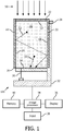
- FIGURE 1 illustrates a first, exemplary embodiment of a unit 100 which detects incoming high energy radiation 50.
- the radiation detector unit 100 may be used, for example, in a computed tomography (CT) imaging apparatus.
- CT is an imaging modality used in many different contexts, including medical imaging.
- CT imaging systems typically employ an x-ray source (not shown) to generate x-rays 50 that traverse an examination region.
- a subject arranged in the examination region interacts with and absorbs a portion of the traversing x-rays 50.
- An array of x-ray radiation detectors 100 is arranged opposite the x-ray source to detect and measure intensities of the transmitted x-rays 50.
- the radiation detector array typically includes several detectors 100, wherein each detector 100 corresponds to one imaging pixel.
- the radiation detector unit 100 may be used in a positron emission tomography (PET) imaging apparatus.
- PET is an imaging modality used in many different contexts, including medical imaging.
- the subject to be imaged typically ingests a radiopharmaceutical which is configured to travel to an area of the subject to be imaged.
- the radiopharmaceutical emits gamma rays 50 which travel through and out of the subject to be detected by an array of gamma ray radiation detectors 100 arranged around the subject to detect and measure intensities of the emitted gamma rays 50.
- the radiation detector array typically includes several detectors 100, wherein each detector 100 corresponds to one imaging pixel.
- the radiation detector 100 operates in substantially the same manner.
- the radiation detector 100 interacts with the incoming radiation 50 to produce electronic signals representative of the intensity and spectrum of radiation 50 received by the detector 100.
- the electronic signals may then be electronically processed to produce a two-dimensional or three-dimensional image of the subject under investigation.
- FIGURE 1 is schematic in nature, meant principally for illustration and not as an exact depiction to scale of the elements shown. Therefore, the dimensions of a given element in relation to the dimensions of other elements as shown in the Figure do not necessarily reflect such relative dimensions as one would find in an actual radiation detector unit. For example, in an actual radiation detector unit, the reflector material 22 would be much thinner in relation to the size of the scintillator 10 than illustrated in the Figure.
- the radiation detector unit 100 includes a scintillating luminescent composition 10 which, from the perspective of the view in FIGURE 1 , has a top face 12, a bottom face 14, and four side faces. Only two side faces 16 and 18 are shown in the Figure.
- the relative terms “top”, “bottom” and “side” have meaning only from the perspective of FIGURE 1 . They do not have any functional significance in the operation of the detector 100.
- the detector 100 may be placed in an imaging apparatus such that the face 12 is actually a bottom face.
- the x-ray detector unit 100 functions to harness the incoming high energy radiation 50 impinging upon the top face 12 and produce an electric signal which is representative of the amount or total energy of detected radiation 50.
- the first step in this process is performed by the scintillator 10, which acts as a transducer by absorbing the energy of the incoming high energy radiation 50 and converting that energy to secondary photons 52.
- the amount of secondary photons 52 produced by the scintillator 10 is thus representative of the incoming radiation energy absorbed within a given reading time period.
- Many different scintillators 10 are known in the art, and various scintillator 10 embodiments are discussed further below. The demands of a particular application may render one or more scintillator(s) 10 particularly suitable or particularly unsuitable for that application.
- the x-ray detector unit 100 includes a photodetector 20 optically coupled to the bottom face 14 of the scintillator 10. Such optical coupling may be achieved by a direct contact, or with intervening elements such as for example filters, transparent or semi-transparent layers, transparent or semi-transparent adhesive, light guides, and the like.
- the photodetector 20 absorbs the energy of the secondary photons 52 produced by the scintillator 10 and converts that energy to an electrical signal.
- the electrical signal produced by the photodetector 20 is representative of the amount of secondary photons 52 impinging upon the photodetector 20, and is thus also representative of the radiation 50 flux entering the detector 100.
- Photodetectors include photomultipliers, photodiodes, and the like.
- the scintillator 10 is covered with a reflector material 22 on each portion of its exterior other than the region where the scintillator 10 is optically coupled to the photodetector 20.
- the reflector material 22 reflects the secondary photons 52, but permits the high energy radiation photons 50 to pass through unaffected.
- the secondary photons 52 must exit the scintillator 10 (if they exit at all) through the photodetector 20 (except some small loss).
- Some secondary photons 52 will be self-absorbed by the scintillator 10 before they can reach the photodetector 20, and some may escape through or around the reflector material 22.
- a radiation shielding or reflecting material 28 is placed in the spaces between the top faces 12 of adjacent units 100.
- common x-ray shielding materials 28 include lead and tungsten, both of which substantially prevent the passage of any x-rays through the shield 28.
- the photodetector 20 has one or more electrical leads 30 connecting the photodetector 20 to a circuit board 32.
- the circuit board 32 receives electrical signals from the photodetector 20 and passes them on to signal processing hardware and further on to an image processor 34.
- the image processor 34 processes electrical signals received from several different radiation detector units 100 to form an image of the subject under investigation according to a mathematical algorithm or algorithms.
- the image can be displayed on an associated display 36.
- a user input 38 may be provided for a user to control the image processor 34.
- the image processor 34 may store related imaging data and other data in a memory 40.
- the luminescent compositions of the present disclosure may be used as an x-ray intensifier screen (not shown).
- the luminescent composition is typically in a powdered form, rather than the ceramic or single crystal form of the scintillator 10 shown in FIGURE 1 .
- the present disclosure particularly pertains to a luminescent composition scintillator having a host matrix which incorporates Ce 3+ as an activator.
- the Ce 3+ may comprise from 0.01% to 10% by atomic number within the host matrix.
- the Ce 3+ dopant shows luminescence in the ultraviolet range due to its spin- and parity-allowed [Xe]5d 1 - [Xe]4f 1 transition.
- the luminescent compositions of the present disclosure may include one or more other doping agents in addition to the Ce 3+ .
- co-activators may include, for example, Pr 3+ , Nd 3+ , Sm 3+ , Eu 3+ , Gd 3+ , Tb 3+ , Dy 3+ , Ho 3+ , Er 3+ , Tm 3+ , or Yb 3+ .
- Typical examples of a suitable host lattice include fluorides, sulphates, and phosphates, in particular:
- the present disclosure also concerns the application of one or several of these luminescent compositions as a ceramic or single crystalline converter for CT imaging scanners, or PET or SPECT imaging scanners. This disclosure further concerns the application of one or several of these luminescent compositions in a luminescent powder layer for x-ray intensifying screens.
- Table 1 Density, Peak Emission, and Decay Time of Luminescent Compositions.
- the luminescent compositions of the present disclosure may further include a diffusion barrier which coats the particles, the ceramic, or the single crystal of the composition.
- the diffusion barrier material operates to substantially prevent diffusion of H 2 O, CO 2 and volatile organic compounds across the diffusion barrier. This enhances the stability of the luminescent composition.
- the luminescent compositions of the present disclosure can be produced and used in the same manner as conventional luminescent compositions, as known by one of ordinary skill in the art.
- KYF 4 :Ce(1%) was prepared and evaluated. Initially, the first three ingredients of the following table were thoroughly blended together in an agate mortar: Ingredient Amount KF 0.852 g (14.7 mmol) YF 3 2.119 g (14.5 mmol) CeF 3 0.029 g (0.18 mmol) KBF 4 0.030 g (1 wt-%) KBF 4 was then added to the initial three ingredient blend, in the amount identified in the table, and the resulting mixture was milled again to form a final blend. The final blend was filled into a glassy-carbon crucible and calcined at 650° C for 6 hours. A small sample of AlF 3 was used as a water scavenger in the tube furnace to trap any water remaining in the stream of dried Nitrogen. After the firing step, samples were powderized by grinding in an agate mortar.
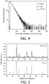
- FIGURE 3 shows the emission 302, excitation 304, and reflection 306 spectra of the resulting KYF 4 :Ce.
- FIGURE 4 shows the decay curve of the resulting KYF 4 :Ce under 265 nm excitation (4f-5d) monitored at 327 nm.
- KY 3 F 10 :Ce(1%) was prepared and evaluated. Initially, the first three ingredients of the following table were thoroughly blended together in an agate mortar: Ingredient Amount KF 0.350 g (6.0 mmol) YF 3 2.614 g (17.9 mmol) CeF 3 0.036 g (0.23 mmol) KBF 4 0.030 g (1 wt-%) KBF 4 was then added to the initial three ingredient blend, in the amount identified in the table, and the resulting mixture was milled again to form a final blend. The final blend was filled into a glassy-carbon crucible and calcined at 650° C for 6 hours. A small sample of AlF 3 was used as a water scavenger in the tube furnace to trap any water remaining in the stream of dried Nitrogen. After the firing step, samples were powderized by grinding in an agate mortar.
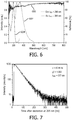
- FIGURE 6 shows the emission 602, excitation 604, and reflection 606 spectra of the resulting KY 3 F 10 :Ce.
- the band at 327 nm is due to an impurity of KYF 4 :Ce.
- FIGURE 7 shows the decay curve of the resulting KY 3 F 10 :Ce under 265 nm excitation (4f-5d) monitored at 377 nm.
- KLaF 4 :Ce(1%) was prepared and evaluated. Initially, the first three ingredients of the following table were thoroughly blended together in an agate mortar: Ingredient Amount KF 0.686 g (11.8 mmol) LaF 3 2.291 g (11.7 mmol) CeF 3 0.029 g (0.18 mmol) KBF 4 0.030 g (1 wt-%) KBF 4 was then added to the initial three ingredient blend, in the amount identified in the table, and the resulting mixture was milled again to form a final blend. The final blend was filled into a glassy-carbon crucible and calcined at 650° C for 6 hours. A small sample of AlF 3 was used as a water scavenger in the tube furnace to trap any water remaining in the stream of dried Nitrogen. After the firing step, samples were powderized by grinding in an agate mortar.
- FIGURE 9 shows the emission 902, excitation 904, and reflection 906 spectra of the resulting KLaF 4 :Ce.
- FIGURE 10 shows the decay curve of the resulting KLaF 4 :Ce under 265 nm excitation (4f-5d) monitored at 317 nm.
- KLuF 4 :Ce(1%) was prepared and evaluated. Initially, the first three ingredients of the following table were thoroughly blended together in an agate mortar: Ingredient Amount KF 0.602 g (10.4 mmol) LuF 3 2.378 g (10.3 mmol) CeF 3 0.020 g (0.13 mmol) KBF 4 0.030 g (1 wt-%) KBF 4 was then added to the initial three ingredient blend, in the amount identified in the table, and the resulting mixture was milled again to form a final blend. The final blend was filled into a glassy-carbon crucible and calcined at 650° C for 6 hours. A small sample of AlF 3 was used as a water scavenger in the tube furnace to trap any water remaining in the stream of dried Nitrogen. After the firing step, samples were powderized by grinding in an agate mortar.
- X-ray diffraction pattern data for un-doped KLuF 4 was not readily available to the inventors at the time this disclosure was prepared.
- FIGURE 12 shows the emission 202, excitation 204, and reflection 206 spectra of the resulting KLuF 4 :Ce.
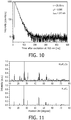
- FIGURE 13 shows the decay curve of the resulting KLuF 4 :Ce under 265 nm excitation (4f-5d) monitored at 312 nm.
- NaYF 4 :Ce(1%) was prepared and evaluated. Initially, the first three ingredients of the following table were thoroughly blended together in an agate mortar: Ingredient Amount NaF 0.669 g (15.9 mmol) YF 3 2.300 g (15.8 mmol) CeF 3 0.031 g (0.19 mmol) NaBF 4 0.030 g (1 wt-%) NaBF 4 was then added to the initial three ingredient blend, in the amount identified in the table, and the resulting mixture was milled again to form a final blend. The final blend was filled into a glassy-carbon crucible and calcined at 700° C for 6 hours. A small sample of AlF 3 was used as a water scavenger in the tube furnace to trap any water remaining in the stream of dried Nitrogen. After the firing step, samples were powderized by grinding in an agate mortar.
- FIGURE 15 shows the emission 502, excitation 504, and reflection 506 spectra of the resulting NaYF 4 :Ce.
- FIGURE 16 shows the decay curve of the resulting NaYF 4 : Ce under 265 nm excitation (4f-5d) monitored at 295 nm.
- NaLuF 4 :Ce(1%) was prepared and evaluated. Initially, the first three ingredients of the following table were thoroughly blended together in an agate mortar: Ingredient Amount NaF 0.460 g (11.0 mmol) LuF 3 2.518 g (10.9 mmol) CeF 3 0.022 g (0.14 mmol) NaBF 4 0.030 g (1 wt-%) NaBF 4 was then added to the initial three ingredient blend, in the amount identified in the table, and the resulting mixture was milled again to form a final blend. The final blend was filled into a glassy-carbon crucible and calcined at 700° C for 6 hours. A small sample of AlF 3 was used as a water scavenger in the tube furnace to trap any water remaining in the stream of dried Nitrogen. After the firing step, samples were powderized by grinding in an agate mortar.
- X-ray diffraction pattern data for un-doped NaLuF 4 was not readily available to the inventors at the time this disclosure was prepared.
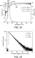
- FIGURE 18 shows a first emission spectrum 802a under 260 nm excitation light, a second emission spectrum 802b under 295 nm excitation light, the excitation spectrum 804, and the reflection spectrum 806 of the resulting NaLuF 4 :Ce.
- FIGURE 19 shows the decay curve of the resulting NaLuF 4 :Ce under 265 nm excitation (4f-5d) monitored at 320 nm.
- RbLaF 4 :Ce(1%) was prepared and evaluated. Initially, the first three ingredients of the following table were thoroughly blended together in an agate mortar: Ingredient Amount RbF 1.043 g (10.0 mmol) LaF 3 1.937 g (9.9 mmol) CeF 3 0.020 g (0.13 mmol) RbBF 4 0.030 g (1 wt-%) RbBF 4 was then added to the initial three ingredient blend, in the amount identified in the table, and the resulting mixture was milled again to form a final blend. The final blend was filled into a glassy-carbon crucible and calcined at 700° C for 6 hours. A small sample of AlF 3 was used as a water scavenger in the tube furnace to trap any water remaining in the stream of dried Nitrogen. After the firing step, samples were powderized by grinding in an agate mortar.
- FIGURE 21 shows the emission 102, excitation 104, and reflection 106 spectra of the resulting RbLaF 4 :Ce.
- FIGURE 22 shows the decay curve of the resulting RbLaF 4 :Ce under 265 nm excitation (4f-5d) monitored at 310 nm.
Landscapes
- Chemical & Material Sciences (AREA)
- Inorganic Chemistry (AREA)
- Engineering & Computer Science (AREA)
- Materials Engineering (AREA)
- Organic Chemistry (AREA)
- Crystallography & Structural Chemistry (AREA)
- Physics & Mathematics (AREA)
- Health & Medical Sciences (AREA)
- Life Sciences & Earth Sciences (AREA)
- General Physics & Mathematics (AREA)
- High Energy & Nuclear Physics (AREA)
- Molecular Biology (AREA)
- Spectroscopy & Molecular Physics (AREA)
- Luminescent Compositions (AREA)
- Measurement Of Radiation (AREA)
- Apparatus For Radiation Diagnosis (AREA)
- Nuclear Medicine (AREA)
Description
- The present application relates generally to the imaging arts and more particularly to luminescent compositions for use in imaging systems. The application subject matter finds use in many kinds of imaging systems, including for example computed tomography (CT) imaging systems, positron emission tomography (PET) imaging systems, and single-photon emission computed tomography (SPECT) systems. It could also be used in connection with other imaging systems, for example as part of an x-ray intensifying screen.
- Luminescent compositions function to harness the energy of incoming high energy radiation photons (e.g. x-rays or gamma rays) and transform that energy to secondary radiation photons (e.g. ultraviolet light) which can more easily be measured by electronic photodetectors such as a photodiode or photomultiplier. Each such transformation is called a scintillation event. The photodetector produces electrical signals indicative of the intensity of the secondary radiation. In a typical application, an imaging detector array includes several pixels, with each pixel formed by one or more blocks of a scintillating luminescent composition material optically coupled to a photodetector.
- The performance of a scintillating luminescent composition material depends on many properties of the material, including for example its stopping power, brightness, and decay time. Ever since the discovery of x-rays by Wilhelm Conrad Roentgen in 1895 there has been an ongoing need to find and develop materials which are efficient in converting higher energy photons into lower energy photons. A wide variety of such scintillating materials have been investigated and used. Commonly used scintillating luminescent compositions for x-ray detection include for example Ce3+ doped inorganic host matrices such as Lu2SiO5, LuPO4, and Lu2Si2O7, all of which have a high density which provides an advantageously high stopping power with respect to the incoming x-ray radiation.
- Nonetheless, novel luminescent compositions are still of high interest, especially if their density or light yield is high, or if their rise and decay times are short. Regarding decay times in particular, a luminescent composition's decay time corresponds to the time it takes for the secondary scintillation light afterglow to fall back down to practically zero or to some other minimum value. Generally speaking, it is desirable to reduce a luminescent composition's decay time. Shorter decay times lead to a shorter imaging time, as well as a higher resolution in the imaging data. Similarly, an afterglow having a narrower wavelength spectrum is preferred to an afterglow having a broader wavelength spectrum. A smaller afterglow is advantageous because it increases the number of scintillation events which may be detected in a given time period, and also increases the temporal resolution of the detector. For these and other reasons the decay time is an essential performance figure of a respective luminescent composition, and shortening of the decay time yields advantages for the application.
- Examples of prior art scintillator materials are known from the following documents.
US2008/213151A1 discloses Pr-containing, garnet-type oxide single crystal scintillator materials.US2010/314550A1 discloses a scintillator for neutron detection, comprising a metal fluoride crystal containing, as constituent elements, a metal having a valence of 2 or higher, such as calcium, aluminum or yttrium; lithium; and fluorine, the metal fluoride crystal containing 1.1 to 20 atoms per unit volume (atoms/nm3) of 6Li, having an effective atomic number of 10 to 40, containing a lanthanoid such as cerium, praseodymium or europium, and being represented by LiCaAlF6, LiSrAlF6, LiYF4 etc.JP 2012 121781 A1 - The present disclosure relates to luminescent compositions sensitized by Ce3+, and in particular to such luminescent compositions in which Ce3+ shows emission in the ultraviolet range. "Ultraviolet" light as defined herein corresponds to light having a wavelength between about 280 nm and about 400 nm. These luminescent compositions include for example scintillating compositions in which Ce3+ is located on crystallographic sites exerting a low crystal-field splitting and a low covalent interaction with the activator. Typical examples are fluorides, sulphates, and phosphates, in particular the following fluorides:
- A(Y1-x-yLuxLay)F4,
- A(Y1-x-yLuxLay)3F10,
- BaCa(Y1-x-yLuxLay)2F10, and
- Ba(Y1-x-yLuxLay)2F8,
- Numerous additional advantages and benefits will become apparent to those of ordinary skill in the art upon reading the following detailed description of the preferred embodiments. The invention may take form in various chemical compositions, various components and arrangements of components, and in various process operations and arrangements of process operations. The drawings are only for the purpose of illustrating preferred embodiments and are not to be construed as limiting the invention.
-
FIGURE 1 is a schematic cross-sectional view of anx-ray detector unit 100, not drawn to scale; -
FIGURE 2 shows the x-ray diffraction pattern of KYF4:Ce (p = 3.53 g/cm3), versus an un-doped KYF4 reference; -
FIGURE 3 shows theemission 302,excitation 304, andreflection 306 spectra of KYF4:Ce; -
FIGURE 4 shows the decay curve of KYF4:Ce under 265 nm excitation (4f-5d) monitored at 327 nm; -
FIGURE 5 shows the x-ray diffraction pattern of KY3F10:Ce (p = 4.27 g/cm3), versus an un-doped KY3F10 reference; -
FIGURE 6 shows theemission 602,excitation 604, andreflection 606 spectra of KY3F10:Ce; -
FIGURE 7 shows the decay curve of KY3F10:Ce under 265 nm excitation (4f-5d) monitored at 377 nm; -
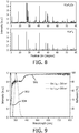
FIGURE 8 shows the x-ray diffraction pattern of KLaF4:Ce (p = 4.46 g/cm3), versus an un-doped KLaF4 reference; -
FIGURE 9 shows theemission 902,excitation 904, andreflection 906 spectra of KLaF4:Ce; -
FIGURE 10 shows the decay curve of KLaF4:Ce under 265 nm excitation (4f-5d) monitored at 317 nm; -
FIGURE 11 shows the x-ray diffraction pattern of KLuF4:Ce (p = 4.80 g/cm3), versus an un-doped KLuF4 reference; -
FIGURE 12 shows theemission 202,excitation 204, andreflection 206 spectra of KLuF4:Ce; -
FIGURE 13 shows the decay curve of KLuF4:Ce under 265 nm excitation (4f-5d) monitored at 312 nm; -
FIGURE 14 shows the x-ray diffraction pattern of NaYF4:Ce (p = 4.30 g/cm3), versus an un-doped NaYF4 reference; -
FIGURE 15 shows theemission 502,excitation 504, andreflection 506 spectra of NaYF4:Ce; -
FIGURE 16 shows the decay curve of NaYF4:Ce under 265 nm excitation (4f-5d) monitored at 295 nm; -
FIGURE 17 shows the x-ray diffraction pattern of NaLuF4:Ce (p = 5.70 g/cm3), versus an un-doped NaYF4 reference; -
FIGURE 18 shows twoemission spectra excitation spectrum 804, and thereflection 806 spectrum of NaLuF4:Ce; -
FIGURE 19 shows the decay curve of NaLuF4:Ce under 265 nm excitation (4f-5d) monitored at 320 nm; -
FIGURE 20 shows the x-ray diffraction pattern of RbLaF4:Ce (p = 4.94 g/cm3), versus an un-doped RbLaF4 reference; -
FIGURE 21 shows theemission 102,excitation 104, andreflection 106 spectra of RbLaF4:Ce; and -
FIGURE 22 shows the decay curve of RbLaF4:Ce under 265 nm excitation (4f-5d) monitored at 310 nm. -
FIGURE 1 illustrates a first, exemplary embodiment of aunit 100 which detects incominghigh energy radiation 50. Theradiation detector unit 100 may be used, for example, in a computed tomography (CT) imaging apparatus. CT is an imaging modality used in many different contexts, including medical imaging. CT imaging systems typically employ an x-ray source (not shown) to generatex-rays 50 that traverse an examination region. A subject arranged in the examination region interacts with and absorbs a portion of the traversingx-rays 50. An array ofx-ray radiation detectors 100 is arranged opposite the x-ray source to detect and measure intensities of the transmittedx-rays 50. The radiation detector array typically includesseveral detectors 100, wherein eachdetector 100 corresponds to one imaging pixel. - In an alternative example, the
radiation detector unit 100 may be used in a positron emission tomography (PET) imaging apparatus. PET is an imaging modality used in many different contexts, including medical imaging. In PET, the subject to be imaged typically ingests a radiopharmaceutical which is configured to travel to an area of the subject to be imaged. The radiopharmaceutical emitsgamma rays 50 which travel through and out of the subject to be detected by an array of gammaray radiation detectors 100 arranged around the subject to detect and measure intensities of the emittedgamma rays 50. The radiation detector array typically includesseveral detectors 100, wherein eachdetector 100 corresponds to one imaging pixel. - Regardless of the particular imaging apparatus, the
radiation detector 100 operates in substantially the same manner. Theradiation detector 100 interacts with theincoming radiation 50 to produce electronic signals representative of the intensity and spectrum ofradiation 50 received by thedetector 100. The electronic signals may then be electronically processed to produce a two-dimensional or three-dimensional image of the subject under investigation.FIGURE 1 is schematic in nature, meant principally for illustration and not as an exact depiction to scale of the elements shown. Therefore, the dimensions of a given element in relation to the dimensions of other elements as shown in the Figure do not necessarily reflect such relative dimensions as one would find in an actual radiation detector unit. For example, in an actual radiation detector unit, thereflector material 22 would be much thinner in relation to the size of thescintillator 10 than illustrated in the Figure. - The
radiation detector unit 100 includes a scintillatingluminescent composition 10 which, from the perspective of the view inFIGURE 1 , has atop face 12, abottom face 14, and four side faces. Only two side faces 16 and 18 are shown in the Figure. The relative terms "top", "bottom" and "side" have meaning only from the perspective ofFIGURE 1 . They do not have any functional significance in the operation of thedetector 100. Thus, in particular applications, thedetector 100 may be placed in an imaging apparatus such that theface 12 is actually a bottom face. - The
x-ray detector unit 100 functions to harness the incominghigh energy radiation 50 impinging upon thetop face 12 and produce an electric signal which is representative of the amount or total energy of detectedradiation 50. The first step in this process is performed by thescintillator 10, which acts as a transducer by absorbing the energy of the incominghigh energy radiation 50 and converting that energy tosecondary photons 52. The amount ofsecondary photons 52 produced by thescintillator 10 is thus representative of the incoming radiation energy absorbed within a given reading time period. Manydifferent scintillators 10 are known in the art, andvarious scintillator 10 embodiments are discussed further below. The demands of a particular application may render one or more scintillator(s) 10 particularly suitable or particularly unsuitable for that application. - The
x-ray detector unit 100 includes aphotodetector 20 optically coupled to thebottom face 14 of thescintillator 10. Such optical coupling may be achieved by a direct contact, or with intervening elements such as for example filters, transparent or semi-transparent layers, transparent or semi-transparent adhesive, light guides, and the like. Thephotodetector 20 absorbs the energy of thesecondary photons 52 produced by thescintillator 10 and converts that energy to an electrical signal. The electrical signal produced by thephotodetector 20 is representative of the amount ofsecondary photons 52 impinging upon thephotodetector 20, and is thus also representative of theradiation 50 flux entering thedetector 100. Photodetectors include photomultipliers, photodiodes, and the like. - The
scintillator 10 is covered with areflector material 22 on each portion of its exterior other than the region where thescintillator 10 is optically coupled to thephotodetector 20. Thereflector material 22 reflects thesecondary photons 52, but permits the highenergy radiation photons 50 to pass through unaffected. Thus, thesecondary photons 52 must exit the scintillator 10 (if they exit at all) through the photodetector 20 (except some small loss). Somesecondary photons 52 will be self-absorbed by thescintillator 10 before they can reach thephotodetector 20, and some may escape through or around thereflector material 22. - To help ensure that each
radiation detector unit 100 counts only theradiation 50 which impinges upon thetop face 12 of thatunit 100, a radiation shielding or reflectingmaterial 28 is placed in the spaces between the top faces 12 ofadjacent units 100. For example, commonx-ray shielding materials 28 include lead and tungsten, both of which substantially prevent the passage of any x-rays through theshield 28. - The
photodetector 20 has one or moreelectrical leads 30 connecting thephotodetector 20 to acircuit board 32. Thecircuit board 32 receives electrical signals from thephotodetector 20 and passes them on to signal processing hardware and further on to animage processor 34. Theimage processor 34 processes electrical signals received from several differentradiation detector units 100 to form an image of the subject under investigation according to a mathematical algorithm or algorithms. The image can be displayed on an associateddisplay 36. Auser input 38 may be provided for a user to control theimage processor 34. Theimage processor 34 may store related imaging data and other data in amemory 40. - In yet another example, the luminescent compositions of the present disclosure may be used as an x-ray intensifier screen (not shown). In such embodiments, the luminescent composition is typically in a powdered form, rather than the ceramic or single crystal form of the
scintillator 10 shown inFIGURE 1 . - The present disclosure particularly pertains to a luminescent composition scintillator having a host matrix which incorporates Ce3+ as an activator. In some embodiments, for example, the Ce3+ may comprise from 0.01% to 10% by atomic number within the host matrix. The Ce3+ dopant shows luminescence in the ultraviolet range due to its spin- and parity-allowed [Xe]5d1 - [Xe]4f1 transition. The luminescent compositions of the present disclosure may include one or more other doping agents in addition to the Ce3+. These co-activators may include, for example, Pr3+, Nd3+, Sm3+, Eu3+, Gd3+, Tb3+, Dy3+, Ho3+, Er3+, Tm3+, or Yb3+. Typical examples of a suitable host lattice include fluorides, sulphates, and phosphates, in particular:
- A(Y1-x-yLuxLay)F4,
- A(Y1-x-yLuxLay)3F10,
- BaCa(Y1-x-yLuxLay)2F10, and
- Ba(Y1-x-yLuxLay)2F8,
- The present disclosure also concerns the application of one or several of these luminescent compositions as a ceramic or single crystalline converter for CT imaging scanners, or PET or SPECT imaging scanners. This disclosure further concerns the application of one or several of these luminescent compositions in a luminescent powder layer for x-ray intensifying screens. The following table gives an overview of some representative example luminescent compositions:
Table 1: Density, Peak Emission, and Decay Time of Luminescent Compositions. Example No. Chemical Composition Density [g/cm3] Emission maximum [nm] Decay time 1/e [ns]1 KYF4:Ce 3.53 327 31 2 KY3F10:Ce 4.27 377 45 3 KLaF4:Ce 4.46 317 26 4 KLuF4:Ce 4.80 312 29 5 NaYF4:Ce 4.30 295 23 6 NaLuF4:Ce 5.70 310 33 7 RbLaF4:Ce 4.94 310 26 8 BaYF5:Ce 5.25 330 41 9 NaLaF4:Ce 4.66 10 KLu3F10:Ce 6.78 11 CsLaF4: Ce 12 BaY2F8:Ce 5.02 13 Ba4Y3F17:Ce 5.24 14 BaLu2F8:Ce 6.98 15 BaCaLu2F10:Ce 6.54 - The luminescent compositions of the present disclosure may further include a diffusion barrier which coats the particles, the ceramic, or the single crystal of the composition. The diffusion barrier material operates to substantially prevent diffusion of H2O, CO2 and volatile organic compounds across the diffusion barrier. This enhances the stability of the luminescent composition.
- The luminescent compositions of the present disclosure can be produced and used in the same manner as conventional luminescent compositions, as known by one of ordinary skill in the art.
- The following working examples are provided to more thoroughly describe exemplary luminescent compositions.
- KYF4:Ce(1%) was prepared and evaluated. Initially, the first three ingredients of the following table were thoroughly blended together in an agate mortar:
Ingredient Amount KF 0.852 g (14.7 mmol) YF3 2.119 g (14.5 mmol) CeF3 0.029 g (0.18 mmol) KBF4 0.030 g (1 wt-%) -
FIGURE 2 shows the x-ray diffraction pattern of the resulting KYF4:Ce (p = 3.53 g/cm3), versus an un-doped KYF4 reference. -
FIGURE 3 shows theemission 302,excitation 304, andreflection 306 spectra of the resulting KYF4:Ce. -
FIGURE 4 shows the decay curve of the resulting KYF4:Ce under 265 nm excitation (4f-5d) monitored at 327 nm. - KY3F10:Ce(1%) was prepared and evaluated. Initially, the first three ingredients of the following table were thoroughly blended together in an agate mortar:
Ingredient Amount KF 0.350 g (6.0 mmol) YF3 2.614 g (17.9 mmol) CeF3 0.036 g (0.23 mmol) KBF4 0.030 g (1 wt-%) -
FIGURE 5 shows the x-ray diffraction pattern of the resulting KY3F10:Ce (p = 4.27 g/cm3), versus an un-doped KY3F10 reference. -
FIGURE 6 shows theemission 602,excitation 604, andreflection 606 spectra of the resulting KY3F10:Ce. The band at 327 nm is due to an impurity of KYF4:Ce. -
FIGURE 7 shows the decay curve of the resulting KY3F10:Ce under 265 nm excitation (4f-5d) monitored at 377 nm. - KLaF4:Ce(1%) was prepared and evaluated. Initially, the first three ingredients of the following table were thoroughly blended together in an agate mortar:
Ingredient Amount KF 0.686 g (11.8 mmol) LaF3 2.291 g (11.7 mmol) CeF3 0.029 g (0.18 mmol) KBF4 0.030 g (1 wt-%) -
FIGURE 8 shows the x-ray diffraction pattern of the resulting KLaF4:Ce (p = 4.46 g/cm3), versus an un-doped KLaF4 reference. -
FIGURE 9 shows theemission 902,excitation 904, andreflection 906 spectra of the resulting KLaF4:Ce. -
FIGURE 10 shows the decay curve of the resulting KLaF4:Ce under 265 nm excitation (4f-5d) monitored at 317 nm. - KLuF4:Ce(1%) was prepared and evaluated. Initially, the first three ingredients of the following table were thoroughly blended together in an agate mortar:
Ingredient Amount KF 0.602 g (10.4 mmol) LuF3 2.378 g (10.3 mmol) CeF3 0.020 g (0.13 mmol) KBF4 0.030 g (1 wt-%) -
FIGURE 11 shows the x-ray diffraction pattern of the resulting KLuF4:Ce (p = 4.80 g/cm3), versus an un-doped KYF4 reference. X-ray diffraction pattern data for un-doped KLuF4 was not readily available to the inventors at the time this disclosure was prepared. -
FIGURE 12 shows theemission 202,excitation 204, andreflection 206 spectra of the resulting KLuF4:Ce. -
FIGURE 13 shows the decay curve of the resulting KLuF4:Ce under 265 nm excitation (4f-5d) monitored at 312 nm. - NaYF4:Ce(1%) was prepared and evaluated. Initially, the first three ingredients of the following table were thoroughly blended together in an agate mortar:
Ingredient Amount NaF 0.669 g (15.9 mmol) YF3 2.300 g (15.8 mmol) CeF3 0.031 g (0.19 mmol) NaBF4 0.030 g (1 wt-%) -
FIGURE 14 shows the x-ray diffraction pattern of the resulting NaYF4:Ce (p = 4.30 g/cm3), versus an un-doped NaYF4 reference. -
FIGURE 15 shows theemission 502,excitation 504, andreflection 506 spectra of the resulting NaYF4:Ce. -
FIGURE 16 shows the decay curve of the resulting NaYF4: Ce under 265 nm excitation (4f-5d) monitored at 295 nm. - NaLuF4:Ce(1%) was prepared and evaluated. Initially, the first three ingredients of the following table were thoroughly blended together in an agate mortar:
Ingredient Amount NaF 0.460 g (11.0 mmol) LuF3 2.518 g (10.9 mmol) CeF3 0.022 g (0.14 mmol) NaBF4 0.030 g (1 wt-%) -
FIGURE 17 shows the x-ray diffraction pattern of the resulting NaLuF4:Ce (p = 5.70 g/cm3), versus an un-doped NaYF4 reference. X-ray diffraction pattern data for un-doped NaLuF4 was not readily available to the inventors at the time this disclosure was prepared. -
FIGURE 18 shows afirst emission spectrum 802a under 260 nm excitation light, asecond emission spectrum 802b under 295 nm excitation light, theexcitation spectrum 804, and thereflection spectrum 806 of the resulting NaLuF4:Ce. -
FIGURE 19 shows the decay curve of the resulting NaLuF4:Ce under 265 nm excitation (4f-5d) monitored at 320 nm. - RbLaF4:Ce(1%) was prepared and evaluated. Initially, the first three ingredients of the following table were thoroughly blended together in an agate mortar:
Ingredient Amount RbF 1.043 g (10.0 mmol) LaF3 1.937 g (9.9 mmol) CeF3 0.020 g (0.13 mmol) RbBF4 0.030 g (1 wt-%) -
FIGURE 20 shows the x-ray diffraction pattern of the resulting RbLaF4:Ce (p = 4.94 g/cm3), versus an un-doped RbLaF4 reference. -
FIGURE 21 shows theemission 102,excitation 104, andreflection 106 spectra of the resulting RbLaF4:Ce. -
FIGURE 22 shows the decay curve of the resulting RbLaF4:Ce under 265 nm excitation (4f-5d) monitored at 310 nm. - The invention has been described with reference to the preferred embodiments. Obviously, modifications and alterations will occur to others upon reading and understanding the preceding detailed description. It is intended that the invention be construed as including all such modifications and alterations insofar as they come within the scope of the appended claims or the equivalents thereof. The invention may take form in various chemical compositions, components and arrangements, combinations and sub-combinations of the elements of the disclosed embodiments.
Claims (14)
- A scintillator material comprising a host lattice activated by Ce3+, wherein the host lattice is selected from the group consisting of:A(Y1-x-yLuxLay)F4,A(Y1-x-yLuxLay)3F10,BaCa(Y1-x-yLuxLay)2F10, andBa(Y1-x-yLuxLay)2F8,and further wherein A is selected from the group consisting of Li, Na, K, Rb, Cs, and a solid solution comprising a mixture of two or more of those elements, and
wherein 0 < x < 1 and 0 < y < 1. - The scintillator material of claim 1, wherein the material is activated by 0.01% to 10% of Ce3+.
- The scintillator material of claim 1, wherein the material is co-activated by at least one element selected from the group consisting of Pr3+, Nd3+, Sm3+, Eu3+, Gd3+, Tb3+, Dy3+, Ho3+, Er3+, Tm3+, and Yb3+.
- The scintillator material of claim 1, further comprising a diffusion barrier coating material which substantially prevents diffusion of H2O, CO2 and volatile organic compounds across the diffusion barrier.
- A PET or SPECT imaging system comprising the scintillator material of claim 1.
- A CT imaging system comprising the scintillator material of claim 1.
- An imaging system including an x-ray converter film which comprises the scintillator material of claim 1.
- A luminescent composition comprising a host matrix in combination with Ce3+ as an activator, in which the emission band maximum of the Ce3+ is equal to or below 400 nm
wherein the host matrix is selected from the group consisting of:A(Y1-x-yLuxLay)F4,A(Y1-x-yLuxLay)3F10,BaCa(Y1-x-yLuxLay)2F10, andBa(Y1-x-yLuxLay)2F8,and further wherein A is selected from the group consisting of Li, Na, K, Rb, Cs, and a solid solution comprising a mixture of two or more of those elements, and
wherein 0 < x < 1 and 0 < y < 1. - The luminescent composition of claim 8, wherein the emission band maximum of the Ce3+ is equal to or above 280 nm.
- The luminescent composition of claim 8, wherein the composition is activated by 0.01% to 10% of Ce3+.
- The luminescent composition of claim 8, wherein the composition is co-activated by at least one element selected from the group consisting of Pr3+, Nd3+, Sm3+, Eu3+, Gd3+, Tb3+, Dy3+, Ho3+, Er3+, Tm3+, and Yb3+.
- The luminescent composition of claim 8, further comprising a diffusion barrier coating material which substantially prevents diffusion of H2O, CO2 and volatile organic compounds across the diffusion barrier.
- An imaging system including an x-ray converter film which comprises the luminescent composition of claim 8.
- A radiation detector including an x-ray converter film which comprises the luminescent composition of claim 8.
Applications Claiming Priority (2)
| Application Number | Priority Date | Filing Date | Title |
|---|---|---|---|
| US201361847101P | 2013-07-17 | 2013-07-17 | |
| PCT/IB2014/063166 WO2015008241A1 (en) | 2013-07-17 | 2014-07-17 | Ce3+ activated luminescent compositions for application in imaging systems |
Publications (2)
| Publication Number | Publication Date |
|---|---|
| EP3030629A1 EP3030629A1 (en) | 2016-06-15 |
| EP3030629B1 true EP3030629B1 (en) | 2018-04-18 |
Family
ID=51542408
Family Applications (1)
| Application Number | Title | Priority Date | Filing Date |
|---|---|---|---|
| EP14766537.6A Not-in-force EP3030629B1 (en) | 2013-07-17 | 2014-07-17 | Ce3+ activated luminescent compositions for application in imaging systems |
Country Status (6)
| Country | Link |
|---|---|
| US (1) | US10018735B2 (en) |
| EP (1) | EP3030629B1 (en) |
| JP (1) | JP6456946B2 (en) |
| CN (1) | CN105378031B (en) |
| RU (1) | RU2016105053A (en) |
| WO (1) | WO2015008241A1 (en) |
Families Citing this family (3)
| Publication number | Priority date | Publication date | Assignee | Title |
|---|---|---|---|---|
| US11673684B2 (en) * | 2020-05-13 | 2023-06-13 | The Boeing Company | System and method for monitoring the structural health of components |
| CN114316984B (en) * | 2021-12-16 | 2023-12-05 | 中国计量大学上虞高等研究院有限公司 | A UV multi-mode responsive fluorescent anti-counterfeiting label |
| CN115368895B (en) * | 2022-07-11 | 2023-12-29 | 昆明理工大学 | Fluoride nanocrystal, preparation method and application thereof |
Family Cites Families (28)
| Publication number | Priority date | Publication date | Assignee | Title |
|---|---|---|---|---|
| US4647781A (en) | 1983-01-31 | 1987-03-03 | Hitachi Chemical Company, Ltd. | Gamma ray detector |
| US5015860A (en) | 1990-04-03 | 1991-05-14 | University Of California | Scintillator materials containing lanthanum fluorides |
| JP2902228B2 (en) * | 1992-10-20 | 1999-06-07 | 富士写真フイルム株式会社 | Radiation image conversion panel and radiation image recording / reproducing method |
| US5483062A (en) | 1994-01-21 | 1996-01-09 | Merrill Corporation | Photon detector based upon an activated lanthanide beryllate scintillator |
| JP2003050280A (en) | 2001-08-03 | 2003-02-21 | Konica Corp | Radiographic image detector |
| FR2847594B1 (en) * | 2002-11-27 | 2004-12-24 | Saint Gobain Cristaux Detecteu | PREPARATION OF RARE EARTH HALIDE BLOCKS |
| US7060982B2 (en) * | 2003-09-24 | 2006-06-13 | Hokushin Corporation | Fluoride single crystal for detecting radiation, scintillator and radiation detector using the single crystal, and method for detecting radiation |
| FR2869115B1 (en) * | 2004-04-14 | 2006-05-26 | Saint Gobain Cristaux Detecteu | RARE EARTH-BASED SCINTILLATOR MATERIAL WITH REDUCED NUCLEAR BACKGROUND NOISE |
| US7405404B1 (en) * | 2004-09-23 | 2008-07-29 | Radiation Monitoring Devices, Inc. | CeBr3 scintillator |
| RU2389835C2 (en) * | 2004-11-08 | 2010-05-20 | Тохоку Текно Арч Ко., Лтд. | Pr-CONTAINING SCINTILLATION MONOCRYSTAL, METHOD OF MAKING SAID CRYSTAL, RADIATION DETECTOR AND INSPECTION DEVICE |
| US7364807B2 (en) | 2004-12-06 | 2008-04-29 | General Electric Company | Thermal barrier coating/environmental barrier coating system for a ceramic-matrix composite (CMC) article to improve high temperature capability |
| US8299436B2 (en) | 2005-06-29 | 2012-10-30 | General Electric Company | High energy resolution scintillators having high light output |
| US7547888B2 (en) | 2005-12-21 | 2009-06-16 | Los Alamos National Security, Llc | Nanocomposite scintillator and detector |
| US8153983B1 (en) * | 2006-05-26 | 2012-04-10 | Radiation Monitoring Devices, Inc. | Gadolinium halide scintillators |
| US7863572B1 (en) * | 2007-07-17 | 2011-01-04 | Sandia Corporation | Fracture-resistant lanthanide scintillators |
| US7655919B1 (en) * | 2007-11-09 | 2010-02-02 | Radiation Monitoring Devices, Inc. | Cesium and lithium-containing quaternary compound scintillators |
| US8575553B1 (en) * | 2007-11-09 | 2013-11-05 | Radiation Monitoring Devices, Inc. | Cesium and sodium-containing scintillator compositions |
| US7767975B2 (en) * | 2007-12-04 | 2010-08-03 | Saint-Gobain Cristaux Et Detecteurs | Ionizing radiation detector |
| US7755054B1 (en) * | 2007-12-17 | 2010-07-13 | Radiation Monitoring Devices, Inc. | Lutetium gadolinium halide scintillators |
| RU2487373C2 (en) * | 2007-12-21 | 2013-07-10 | Конинклейке Филипс Электроникс Н.В. | Radiation-sensitive detector with scintillator in composite resin |
| KR101538194B1 (en) * | 2008-03-24 | 2015-07-20 | 가부시끼가이샤 도꾸야마 | Scintillator for neutron detection and neutron detector |
| US8440980B2 (en) * | 2009-08-03 | 2013-05-14 | Radiation Monitoring Devices, Inc. | CsLiLn halide scintillator |
| US8981311B2 (en) * | 2010-05-24 | 2015-03-17 | Koninklijke Philips N.V. | CT detector including multi-layer fluorescent tape scintillator with switchable spectral sensitivity |
| JP5455881B2 (en) * | 2010-12-10 | 2014-03-26 | 株式会社トクヤマ | Fluoride single crystal, vacuum ultraviolet light emitting device and scintillator |
| CN103131418B (en) * | 2011-11-23 | 2017-04-12 | 通用电气公司 | Ce3+ Activated Mixed Halide Potassium Cryolite and High Energy Resolution Scintillator |
| US9230683B2 (en) | 2012-04-25 | 2016-01-05 | Semiconductor Energy Laboratory Co., Ltd. | Semiconductor device and driving method thereof |
| US9334444B1 (en) * | 2014-02-11 | 2016-05-10 | Sandia Corporation | Sorohalide scintillators, phosphors, and uses thereof |
| US9561969B2 (en) * | 2014-04-18 | 2017-02-07 | University Of Tennessee Research Foundation | Intrinsic complex halide elpasolite scintillators and methods of making and using same |
-
2014
- 2014-07-17 EP EP14766537.6A patent/EP3030629B1/en not_active Not-in-force
- 2014-07-17 US US14/903,640 patent/US10018735B2/en active Active
- 2014-07-17 CN CN201480040286.4A patent/CN105378031B/en active Active
- 2014-07-17 WO PCT/IB2014/063166 patent/WO2015008241A1/en not_active Ceased
- 2014-07-17 RU RU2016105053A patent/RU2016105053A/en unknown
- 2014-07-17 JP JP2016526743A patent/JP6456946B2/en active Active
Non-Patent Citations (1)
| Title |
|---|
| None * |
Also Published As
| Publication number | Publication date |
|---|---|
| CN105378031B (en) | 2019-04-19 |
| JP6456946B2 (en) | 2019-01-23 |
| JP2016531976A (en) | 2016-10-13 |
| WO2015008241A1 (en) | 2015-01-22 |
| EP3030629A1 (en) | 2016-06-15 |
| CN105378031A (en) | 2016-03-02 |
| US10018735B2 (en) | 2018-07-10 |
| US20160146950A1 (en) | 2016-05-26 |
| RU2016105053A (en) | 2017-08-21 |
Similar Documents
| Publication | Publication Date | Title |
|---|---|---|
| KR100706705B1 (en) | Scintillation crystals and how to make them and how to use them | |
| Lempicki et al. | A new lutetia-based ceramic scintillator for X-ray imaging | |
| RU2638158C2 (en) | Scintillator composition, radiation detector device and high-energy radiation recording method | |
| CN101479361B (en) | Scintillating materials, methods for fabricating the same, and methods for their use | |
| EP1043383B1 (en) | Phosphors, and radiation detectors and x-ray ct unit made by using the same | |
| RU2423725C2 (en) | Scintillators for detecting radiation, as well as corresponding methods and devices | |
| US9175216B2 (en) | Ceramic scintillator body and scintillation device | |
| US9193903B2 (en) | Solid scintillator, radiation detector, and radiation examination device | |
| EP1739150B1 (en) | High energy resolution scintillators having high light output | |
| JP5281742B2 (en) | Scintillator material and radiation detector containing scintillator material | |
| US20120145962A1 (en) | Solid state scintillator material, solid state scintillator, radiation detector, and radiation inspection apparatus | |
| US8083968B2 (en) | Solid scintillator, radiation detector, and X-ray tomographic imaging apparatus | |
| KR20060019562A (en) | Rare Earth Iodide Flash Crystals | |
| JP6776671B2 (en) | Fluorescent materials, ceramic scintillators and radiation detectors, and methods for manufacturing fluorescent materials | |
| EP1279717B1 (en) | Phosphor, radiation detector containing the same, and x-ray ct apparatus | |
| US10018735B2 (en) | CE3+ activated luminescent compositions for application in imaging systems | |
| JP5937287B1 (en) | Mixed oxide material | |
| TW201521685A (en) | Scintillator material, radiation detector, and radiographic examination device | |
| JP4678924B2 (en) | Radiation detector and X-ray diagnostic apparatus using the same | |
| JP7302706B2 (en) | Ceramic scintillators and radiation detectors | |
| US20100127176A1 (en) | Scintillator materials which absorb high-energy, and related methods and devices | |
| US20120313013A1 (en) | Scintillator plate | |
| JP7160572B2 (en) | radiation monitor | |
| US10908301B2 (en) | Radiation monitor |
Legal Events
| Date | Code | Title | Description |
|---|---|---|---|
| PUAI | Public reference made under article 153(3) epc to a published international application that has entered the european phase |
Free format text: ORIGINAL CODE: 0009012 |
|
| 17P | Request for examination filed |
Effective date: 20160217 |
|
| AK | Designated contracting states |
Kind code of ref document: A1 Designated state(s): AL AT BE BG CH CY CZ DE DK EE ES FI FR GB GR HR HU IE IS IT LI LT LU LV MC MK MT NL NO PL PT RO RS SE SI SK SM TR |
|
| AX | Request for extension of the european patent |
Extension state: BA ME |
|
| DAX | Request for extension of the european patent (deleted) | ||
| 17Q | First examination report despatched |
Effective date: 20170411 |
|
| GRAP | Despatch of communication of intention to grant a patent |
Free format text: ORIGINAL CODE: EPIDOSNIGR1 |
|
| RIC1 | Information provided on ipc code assigned before grant |
Ipc: G01T 1/202 20060101ALI20171011BHEP Ipc: C09K 11/77 20060101AFI20171011BHEP |
|
| INTG | Intention to grant announced |
Effective date: 20171116 |
|
| GRAS | Grant fee paid |
Free format text: ORIGINAL CODE: EPIDOSNIGR3 |
|
| GRAA | (expected) grant |
Free format text: ORIGINAL CODE: 0009210 |
|
| AK | Designated contracting states |
Kind code of ref document: B1 Designated state(s): AL AT BE BG CH CY CZ DE DK EE ES FI FR GB GR HR HU IE IS IT LI LT LU LV MC MK MT NL NO PL PT RO RS SE SI SK SM TR |
|
| REG | Reference to a national code |
Ref country code: GB Ref legal event code: FG4D |
|
| REG | Reference to a national code |
Ref country code: CH Ref legal event code: EP |
|
| REG | Reference to a national code |
Ref country code: AT Ref legal event code: REF Ref document number: 990456 Country of ref document: AT Kind code of ref document: T Effective date: 20180515 |
|
| REG | Reference to a national code |
Ref country code: IE Ref legal event code: FG4D |
|
| REG | Reference to a national code |
Ref country code: DE Ref legal event code: R096 Ref document number: 602014024137 Country of ref document: DE |
|
| REG | Reference to a national code |
Ref country code: FR Ref legal event code: PLFP Year of fee payment: 5 |
|
| REG | Reference to a national code |
Ref country code: NL Ref legal event code: MP Effective date: 20180418 |
|
| REG | Reference to a national code |
Ref country code: LT Ref legal event code: MG4D |
|
| PG25 | Lapsed in a contracting state [announced via postgrant information from national office to epo] |
Ref country code: NL Free format text: LAPSE BECAUSE OF FAILURE TO SUBMIT A TRANSLATION OF THE DESCRIPTION OR TO PAY THE FEE WITHIN THE PRESCRIBED TIME-LIMIT Effective date: 20180418 |
|
| PG25 | Lapsed in a contracting state [announced via postgrant information from national office to epo] |
Ref country code: ES Free format text: LAPSE BECAUSE OF FAILURE TO SUBMIT A TRANSLATION OF THE DESCRIPTION OR TO PAY THE FEE WITHIN THE PRESCRIBED TIME-LIMIT Effective date: 20180418 Ref country code: LT Free format text: LAPSE BECAUSE OF FAILURE TO SUBMIT A TRANSLATION OF THE DESCRIPTION OR TO PAY THE FEE WITHIN THE PRESCRIBED TIME-LIMIT Effective date: 20180418 Ref country code: FI Free format text: LAPSE BECAUSE OF FAILURE TO SUBMIT A TRANSLATION OF THE DESCRIPTION OR TO PAY THE FEE WITHIN THE PRESCRIBED TIME-LIMIT Effective date: 20180418 Ref country code: BG Free format text: LAPSE BECAUSE OF FAILURE TO SUBMIT A TRANSLATION OF THE DESCRIPTION OR TO PAY THE FEE WITHIN THE PRESCRIBED TIME-LIMIT Effective date: 20180718 Ref country code: PL Free format text: LAPSE BECAUSE OF FAILURE TO SUBMIT A TRANSLATION OF THE DESCRIPTION OR TO PAY THE FEE WITHIN THE PRESCRIBED TIME-LIMIT Effective date: 20180418 Ref country code: NO Free format text: LAPSE BECAUSE OF FAILURE TO SUBMIT A TRANSLATION OF THE DESCRIPTION OR TO PAY THE FEE WITHIN THE PRESCRIBED TIME-LIMIT Effective date: 20180718 Ref country code: AL Free format text: LAPSE BECAUSE OF FAILURE TO SUBMIT A TRANSLATION OF THE DESCRIPTION OR TO PAY THE FEE WITHIN THE PRESCRIBED TIME-LIMIT Effective date: 20180418 Ref country code: SE Free format text: LAPSE BECAUSE OF FAILURE TO SUBMIT A TRANSLATION OF THE DESCRIPTION OR TO PAY THE FEE WITHIN THE PRESCRIBED TIME-LIMIT Effective date: 20180418 |
|
| PG25 | Lapsed in a contracting state [announced via postgrant information from national office to epo] |
Ref country code: GR Free format text: LAPSE BECAUSE OF FAILURE TO SUBMIT A TRANSLATION OF THE DESCRIPTION OR TO PAY THE FEE WITHIN THE PRESCRIBED TIME-LIMIT Effective date: 20180719 Ref country code: LV Free format text: LAPSE BECAUSE OF FAILURE TO SUBMIT A TRANSLATION OF THE DESCRIPTION OR TO PAY THE FEE WITHIN THE PRESCRIBED TIME-LIMIT Effective date: 20180418 Ref country code: RS Free format text: LAPSE BECAUSE OF FAILURE TO SUBMIT A TRANSLATION OF THE DESCRIPTION OR TO PAY THE FEE WITHIN THE PRESCRIBED TIME-LIMIT Effective date: 20180418 Ref country code: HR Free format text: LAPSE BECAUSE OF FAILURE TO SUBMIT A TRANSLATION OF THE DESCRIPTION OR TO PAY THE FEE WITHIN THE PRESCRIBED TIME-LIMIT Effective date: 20180418 |
|
| REG | Reference to a national code |
Ref country code: AT Ref legal event code: MK05 Ref document number: 990456 Country of ref document: AT Kind code of ref document: T Effective date: 20180418 |
|
| PG25 | Lapsed in a contracting state [announced via postgrant information from national office to epo] |
Ref country code: PT Free format text: LAPSE BECAUSE OF FAILURE TO SUBMIT A TRANSLATION OF THE DESCRIPTION OR TO PAY THE FEE WITHIN THE PRESCRIBED TIME-LIMIT Effective date: 20180820 |
|
| REG | Reference to a national code |
Ref country code: DE Ref legal event code: R097 Ref document number: 602014024137 Country of ref document: DE |
|
| PG25 | Lapsed in a contracting state [announced via postgrant information from national office to epo] |
Ref country code: CZ Free format text: LAPSE BECAUSE OF FAILURE TO SUBMIT A TRANSLATION OF THE DESCRIPTION OR TO PAY THE FEE WITHIN THE PRESCRIBED TIME-LIMIT Effective date: 20180418 Ref country code: SK Free format text: LAPSE BECAUSE OF FAILURE TO SUBMIT A TRANSLATION OF THE DESCRIPTION OR TO PAY THE FEE WITHIN THE PRESCRIBED TIME-LIMIT Effective date: 20180418 Ref country code: RO Free format text: LAPSE BECAUSE OF FAILURE TO SUBMIT A TRANSLATION OF THE DESCRIPTION OR TO PAY THE FEE WITHIN THE PRESCRIBED TIME-LIMIT Effective date: 20180418 Ref country code: DK Free format text: LAPSE BECAUSE OF FAILURE TO SUBMIT A TRANSLATION OF THE DESCRIPTION OR TO PAY THE FEE WITHIN THE PRESCRIBED TIME-LIMIT Effective date: 20180418 Ref country code: EE Free format text: LAPSE BECAUSE OF FAILURE TO SUBMIT A TRANSLATION OF THE DESCRIPTION OR TO PAY THE FEE WITHIN THE PRESCRIBED TIME-LIMIT Effective date: 20180418 Ref country code: AT Free format text: LAPSE BECAUSE OF FAILURE TO SUBMIT A TRANSLATION OF THE DESCRIPTION OR TO PAY THE FEE WITHIN THE PRESCRIBED TIME-LIMIT Effective date: 20180418 |
|
| PLBE | No opposition filed within time limit |
Free format text: ORIGINAL CODE: 0009261 |
|
| STAA | Information on the status of an ep patent application or granted ep patent |
Free format text: STATUS: NO OPPOSITION FILED WITHIN TIME LIMIT |
|
| PG25 | Lapsed in a contracting state [announced via postgrant information from national office to epo] |
Ref country code: SM Free format text: LAPSE BECAUSE OF FAILURE TO SUBMIT A TRANSLATION OF THE DESCRIPTION OR TO PAY THE FEE WITHIN THE PRESCRIBED TIME-LIMIT Effective date: 20180418 Ref country code: IT Free format text: LAPSE BECAUSE OF FAILURE TO SUBMIT A TRANSLATION OF THE DESCRIPTION OR TO PAY THE FEE WITHIN THE PRESCRIBED TIME-LIMIT Effective date: 20180418 |
|
| REG | Reference to a national code |
Ref country code: CH Ref legal event code: PL |
|
| 26N | No opposition filed |
Effective date: 20190121 |
|
| GBPC | Gb: european patent ceased through non-payment of renewal fee |
Effective date: 20180718 |
|
| PG25 | Lapsed in a contracting state [announced via postgrant information from national office to epo] |
Ref country code: MC Free format text: LAPSE BECAUSE OF FAILURE TO SUBMIT A TRANSLATION OF THE DESCRIPTION OR TO PAY THE FEE WITHIN THE PRESCRIBED TIME-LIMIT Effective date: 20180418 Ref country code: LU Free format text: LAPSE BECAUSE OF NON-PAYMENT OF DUE FEES Effective date: 20180717 |
|
| REG | Reference to a national code |
Ref country code: BE Ref legal event code: MM Effective date: 20180731 |
|
| REG | Reference to a national code |
Ref country code: IE Ref legal event code: MM4A |
|
| PG25 | Lapsed in a contracting state [announced via postgrant information from national office to epo] |
Ref country code: GB Free format text: LAPSE BECAUSE OF NON-PAYMENT OF DUE FEES Effective date: 20180718 Ref country code: IE Free format text: LAPSE BECAUSE OF NON-PAYMENT OF DUE FEES Effective date: 20180717 Ref country code: LI Free format text: LAPSE BECAUSE OF NON-PAYMENT OF DUE FEES Effective date: 20180731 Ref country code: CH Free format text: LAPSE BECAUSE OF NON-PAYMENT OF DUE FEES Effective date: 20180731 |
|
| PG25 | Lapsed in a contracting state [announced via postgrant information from national office to epo] |
Ref country code: SI Free format text: LAPSE BECAUSE OF FAILURE TO SUBMIT A TRANSLATION OF THE DESCRIPTION OR TO PAY THE FEE WITHIN THE PRESCRIBED TIME-LIMIT Effective date: 20180418 Ref country code: BE Free format text: LAPSE BECAUSE OF NON-PAYMENT OF DUE FEES Effective date: 20180731 |
|
| PG25 | Lapsed in a contracting state [announced via postgrant information from national office to epo] |
Ref country code: MT Free format text: LAPSE BECAUSE OF NON-PAYMENT OF DUE FEES Effective date: 20180717 |
|
| PG25 | Lapsed in a contracting state [announced via postgrant information from national office to epo] |
Ref country code: TR Free format text: LAPSE BECAUSE OF FAILURE TO SUBMIT A TRANSLATION OF THE DESCRIPTION OR TO PAY THE FEE WITHIN THE PRESCRIBED TIME-LIMIT Effective date: 20180418 |
|
| PG25 | Lapsed in a contracting state [announced via postgrant information from national office to epo] |
Ref country code: HU Free format text: LAPSE BECAUSE OF FAILURE TO SUBMIT A TRANSLATION OF THE DESCRIPTION OR TO PAY THE FEE WITHIN THE PRESCRIBED TIME-LIMIT; INVALID AB INITIO Effective date: 20140717 Ref country code: CY Free format text: LAPSE BECAUSE OF FAILURE TO SUBMIT A TRANSLATION OF THE DESCRIPTION OR TO PAY THE FEE WITHIN THE PRESCRIBED TIME-LIMIT Effective date: 20180418 Ref country code: MK Free format text: LAPSE BECAUSE OF NON-PAYMENT OF DUE FEES Effective date: 20180418 |
|
| PG25 | Lapsed in a contracting state [announced via postgrant information from national office to epo] |
Ref country code: IS Free format text: LAPSE BECAUSE OF FAILURE TO SUBMIT A TRANSLATION OF THE DESCRIPTION OR TO PAY THE FEE WITHIN THE PRESCRIBED TIME-LIMIT Effective date: 20180818 |
|
| REG | Reference to a national code |
Ref country code: DE Ref legal event code: R084 Ref document number: 602014024137 Country of ref document: DE |
|
| PGFP | Annual fee paid to national office [announced via postgrant information from national office to epo] |
Ref country code: DE Payment date: 20240730 Year of fee payment: 11 |
|
| PGFP | Annual fee paid to national office [announced via postgrant information from national office to epo] |
Ref country code: FR Payment date: 20240725 Year of fee payment: 11 |
|
| REG | Reference to a national code |
Ref country code: DE Ref legal event code: R119 Ref document number: 602014024137 Country of ref document: DE |
|
| PG25 | Lapsed in a contracting state [announced via postgrant information from national office to epo] |
Ref country code: DE Free format text: LAPSE BECAUSE OF NON-PAYMENT OF DUE FEES Effective date: 20260203 |
|
| PG25 | Lapsed in a contracting state [announced via postgrant information from national office to epo] |
Ref country code: FR Free format text: LAPSE BECAUSE OF NON-PAYMENT OF DUE FEES Effective date: 20250731 |