EP3030059A1 - An electronic component and corresponding mounting method - Google Patents
An electronic component and corresponding mounting method Download PDFInfo
- Publication number
- EP3030059A1 EP3030059A1 EP15192592.2A EP15192592A EP3030059A1 EP 3030059 A1 EP3030059 A1 EP 3030059A1 EP 15192592 A EP15192592 A EP 15192592A EP 3030059 A1 EP3030059 A1 EP 3030059A1
- Authority
- EP
- European Patent Office
- Prior art keywords
- electrical contact
- contact pad
- electronic component
- soldering area
- pad
- Prior art date
- Legal status (The legal status is an assumption and is not a legal conclusion. Google has not performed a legal analysis and makes no representation as to the accuracy of the status listed.)
- Granted
Links
Images


Classifications
-
- F—MECHANICAL ENGINEERING; LIGHTING; HEATING; WEAPONS; BLASTING
- F21—LIGHTING
- F21V—FUNCTIONAL FEATURES OR DETAILS OF LIGHTING DEVICES OR SYSTEMS THEREOF; STRUCTURAL COMBINATIONS OF LIGHTING DEVICES WITH OTHER ARTICLES, NOT OTHERWISE PROVIDED FOR
- F21V19/00—Fastening of light sources or lamp holders
- F21V19/001—Fastening of light sources or lamp holders the light sources being semiconductors devices, e.g. LEDs
- F21V19/0015—Fastening arrangements intended to retain light sources
- F21V19/0025—Fastening arrangements intended to retain light sources the fastening means engaging the conductors of the light source, i.e. providing simultaneous fastening of the light sources and their electric connections
-
- H—ELECTRICITY
- H10—SEMICONDUCTOR DEVICES; ELECTRIC SOLID-STATE DEVICES NOT OTHERWISE PROVIDED FOR
- H10H—INORGANIC LIGHT-EMITTING SEMICONDUCTOR DEVICES HAVING POTENTIAL BARRIERS
- H10H20/00—Individual inorganic light-emitting semiconductor devices having potential barriers, e.g. light-emitting diodes [LED]
- H10H20/80—Constructional details
- H10H20/85—Packages
- H10H20/858—Means for heat extraction or cooling
- H10H20/8585—Means for heat extraction or cooling being an interconnection
-
- H—ELECTRICITY
- H05—ELECTRIC TECHNIQUES NOT OTHERWISE PROVIDED FOR
- H05K—PRINTED CIRCUITS; CASINGS OR CONSTRUCTIONAL DETAILS OF ELECTRIC APPARATUS; MANUFACTURE OF ASSEMBLAGES OF ELECTRICAL COMPONENTS
- H05K1/00—Printed circuits
- H05K1/02—Details
- H05K1/11—Printed elements for providing electric connections to or between printed circuits
- H05K1/111—Pads for surface mounting, e.g. lay-out
-
- H—ELECTRICITY
- H05—ELECTRIC TECHNIQUES NOT OTHERWISE PROVIDED FOR
- H05K—PRINTED CIRCUITS; CASINGS OR CONSTRUCTIONAL DETAILS OF ELECTRIC APPARATUS; MANUFACTURE OF ASSEMBLAGES OF ELECTRICAL COMPONENTS
- H05K2201/00—Indexing scheme relating to printed circuits covered by H05K1/00
- H05K2201/10—Details of components or other objects attached to or integrated in a printed circuit board
- H05K2201/10007—Types of components
- H05K2201/10106—Light emitting diode [LED]
-
- H—ELECTRICITY
- H05—ELECTRIC TECHNIQUES NOT OTHERWISE PROVIDED FOR
- H05K—PRINTED CIRCUITS; CASINGS OR CONSTRUCTIONAL DETAILS OF ELECTRIC APPARATUS; MANUFACTURE OF ASSEMBLAGES OF ELECTRICAL COMPONENTS
- H05K3/00—Apparatus or processes for manufacturing printed circuits
- H05K3/30—Assembling printed circuits with electric components, e.g. with resistors
- H05K3/32—Assembling printed circuits with electric components, e.g. with resistors electrically connecting electric components or wires to printed circuits
- H05K3/34—Assembling printed circuits with electric components, e.g. with resistors electrically connecting electric components or wires to printed circuits by soldering
- H05K3/341—Surface mounted components
- H05K3/3431—Leadless components
-
- H—ELECTRICITY
- H05—ELECTRIC TECHNIQUES NOT OTHERWISE PROVIDED FOR
- H05K—PRINTED CIRCUITS; CASINGS OR CONSTRUCTIONAL DETAILS OF ELECTRIC APPARATUS; MANUFACTURE OF ASSEMBLAGES OF ELECTRICAL COMPONENTS
- H05K3/00—Apparatus or processes for manufacturing printed circuits
- H05K3/30—Assembling printed circuits with electric components, e.g. with resistors
- H05K3/32—Assembling printed circuits with electric components, e.g. with resistors electrically connecting electric components or wires to printed circuits
- H05K3/34—Assembling printed circuits with electric components, e.g. with resistors electrically connecting electric components or wires to printed circuits by soldering
- H05K3/341—Surface mounted components
- H05K3/3431—Leadless components
- H05K3/3436—Leadless components having an array of bottom contacts, e.g. pad grid array or ball grid array components
-
- H—ELECTRICITY
- H10—SEMICONDUCTOR DEVICES; ELECTRIC SOLID-STATE DEVICES NOT OTHERWISE PROVIDED FOR
- H10H—INORGANIC LIGHT-EMITTING SEMICONDUCTOR DEVICES HAVING POTENTIAL BARRIERS
- H10H20/00—Individual inorganic light-emitting semiconductor devices having potential barriers, e.g. light-emitting diodes [LED]
- H10H20/80—Constructional details
- H10H20/85—Packages
- H10H20/857—Interconnections, e.g. lead-frames, bond wires or solder balls
Definitions
- the present description relates to electronic components.
- One or more embodiments may refer to electronic components such as solid-state light radiation sources, e.g. LED sources, adapted to be mounted onto boards.
- electronic components such as solid-state light radiation sources, e.g. LED sources, adapted to be mounted onto boards.
- Solid-state lighting modules such as LED lighting modules
- high light flux e.g. > 10,000 lm
- high power efficiency e.g. > 120 lm/W
- low cost e.g. > 2 kV AC
- high electrical insulation e.g. > 2 kV AC
- high reliability e.g. only 5% of LED modules may experience a failure after 100,000 working hours.
- thermo-mechanical stresses such as the strain induced during thermal cycles by a mismatch in the CTEs (Coefficient of Thermal Expansion) of the component (e.g. the LED), the solder joints and the mounting board, e.g. the Printed Circuit Board (PCB).
- CTEs Coefficient of Thermal Expansion
- PCB Printed Circuit Board
- Still another solution may be the use of components (e.g. LEDs) with a plastic package.
- components e.g. LEDs
- One or more embodiments aim at overcoming the previously outlined drawbacks.
- said object is achieved thanks to an electronic component having the features set forth in the claims that follow.
- One or more embodiments may concern a corresponding method.
- One or more embodiments may lead to an improvement of reliability of solder joints without affecting the performances of the component (e.g., of the LED) and/or of the board or of the solder paste.
- One or more embodiments may be based on the implementation, if necessary in combination, of one or more of the following features:
- One or more embodiments enable to improve the solder-joint reliability in PBAs without affecting the performances of the component (e.g. LED) or requiring modifications in the board or in the solder paste.
- the component e.g. LED
- One or more embodiments may be used with packages of various kinds (therefore, not only with ceramic packages) and with solder pastes which are deposited in different ways.
- One or various embodiments allow moreover to determine the arrangement of the electrical pads according to the application needs, e.g. according to the package size.
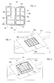
- Figure 1 shows an electronic component 10 adapted to be mounted onto a mounting board 12 (see for example Figures 4 and 5 ) for example a PCB (Printed Circuit Board).
- a mounting board 12 see for example Figures 4 and 5
- PCB Printed Circuit Board
- Electronic component 10 may be for example a solid-state light radiation source, e.g. a LED light radiation source, such as a power LED.
- a solid-state light radiation source e.g. a LED light radiation source, such as a power LED.
- Such an electronic component may comprise a so-called package 14, e.g. a ceramic package, which is provided on the underside with pads enabling the mounting of component 10 onto a board 12, e.g. an IMS (Insulated Metal Substrate) board, by ensuring the electrical contact thereof with supply circuits (which are not visible in the Figures).
- package 14 e.g. a ceramic package, which is provided on the underside with pads enabling the mounting of component 10 onto a board 12, e.g. an IMS (Insulated Metal Substrate) board, by ensuring the electrical contact thereof with supply circuits (which are not visible in the Figures).
- IMS Insulated Metal Substrate
- component 10 (specifically the back side thereof, which will face mounting board 12) may comprise:
- Such a component 10 may be mounted onto a board 12 (e.g. a PCB of the IMS type) by resorting to a layout of mounting contacts formed via known techniques onto the surface of board 12, comprising e.g. a material such as copper, so as to be both electrically and thermally conductive. These contacts define land areas which are adapted to cooperate with pads 16, 18 and 20 provided on electronic component 10.
- a board 12 e.g. a PCB of the IMS type
- solder pastes may be used which are adapted to be interposed between each pad and a corresponding land area.
- anode and cathode electrical contact pads 16 and 18, as well as thermal contact pads 20, may be seen as being distributed over the whole back surface of component 10 (the face which will be mounted onto board 12).
- Such a soldering area includes a central portion CA surrounded by a peripheral or outer portion PA.
- One or more embodiments may be applied to an electronic component 10 as exemplified in Figure 2 , i.e. for example to a solid-state lighting source wherein, mounted in a package 14, e.g. a ceramic package, there is provided a LED radiation source 22 with possible associated optics 24.
- an arrangement may be provided having at least one first electrical contact pad located in central portion CA of the soldering area, and at least one second electrical contact pad located in peripheral portion PA.
- One or more embodiments may omit thermal contact pads such as pad 20 of Figure 1 , while conferring the thermal dissipation function only to anode 16 and cathode 18, as they may consist of a material (e.g. a metal) being both electrically and thermally conductive.
- a material e.g. a metal
- anode pad 16 and cathode pad 18 are distributed practically over the whole soldering area (and therefore both on central portion CA and on peripheral portion PA), so as to perform, in addition to the electrical contact function, an action of thermal dissipation as well, without the need to provide a thermal contact pad 20.
- anode 16 and cathode 18 electrical contact pads may occupy a portion of the soldering area amounting to at least 50% of such soldering area, preferably to at least 70% of the soldering area, and most preferably to at least 90% of the soldering area, comprising central portion CA and peripheral portion PA.
- anode 16 and cathode 18 electrical contact pads are "split" into two arrays according to a e.g. 4x4 matrix, which may be centred around central portion CA of the soldering area and may comprise:
- One or more embodiments as exemplified in Figure 3 may therefore envisage at least one first electrical contact pad (16a or 18a) arranged in central portion CA of the soldering area, and at least one second electrical contact pad 16b, 18b arranged in peripheral portion PA of the soldering area.
- each array i.e. respectively the anode array (pad 16a, 16b) and the cathode array (pad 18a, 18b) comprising at least one first pad 16a, 18a arranged in central portion CA and at least one second pad 16b, 18b arranged in peripheral portion PA of the soldering area.
- the electrical connection between the pads of the respective arrays may be ensured e.g. through a short-circuit effect on the level of an electrically conductive (e.g. metal) interconnect layer 26, which is arranged on the front side of package 14 of device 10: see Figure 2 .
- an electrically conductive (e.g. metal) interconnect layer 26 which is arranged on the front side of package 14 of device 10: see Figure 2 .
- the creep strain due to thermal cycles may grow as a function of the distance from the centre of component 10 (portion CA) and therefore have peak levels at the corners of package 14. These may correspond to the outer corners of both pad arrays 16a, 16b and 18a, 18b shown in Figure 3 , with the consequent possible crack initiation at such corner portions.
- the splitting of electrical contact pads into multiple elements 16a, 16b and 18a, 18b contrasts crack propagation: although they are electrically connected with each other (e.g. one or more layers 26 on the front side of component 10), the various pads are physically separated from one another.
- Figures 4 and 5 exemplify possible mounting options of a device 10 having electrical contact pads 16a, 16b and 18a, 18b, as exemplified in Figure 3 .
- Figure 4 exemplifies the possibility of using solder pastes which are applied (according to known criteria) onto board 12.
- electrically conductive lines respectively an anode track 260 and a cathode track 280, on which there may be applied, for example by silk-screen printing with a solder mask 56, individual solder pastes 360, 380 on corresponding land areas, each solder paste 360, 380 being adapted to be interposed between a respective electrical contact pad 16a, 16b, 18a, 18b and a corresponding land area.
- such a result may be obtained either by splitting land areas into respective elements, on each of which a corresponding solder mask is applied, or by using a solder mask which is split into various distinct portions, so as to have respective window portions at each land area, or by using both solutions combined, i.e. by employing both land areas split into several portions and several separate portions of masking window.
- distinct solder pastes 360, 380 may be implemented, having a distribution corresponding to elements 16a and 16b and 18a, 18b respectively of anode and cathode contact pads.
- FIG. 6 and the following Figures exemplify embodiments which employ the same principle of having electrical contact (respectively anode and cathode) pads which also perform thermal dissipation, with a consequent elimination of thermal contact pad 20 adopted in conventional solutions such as depicted in Figure 1 .
- the solution moreover comprises:
- Figure 7 shows one or more embodiments wherein central contact pad 18 shows a radial extension 1800 extending towards peripheral portion PA with a width which is shorter than the width of the portion of central pad 18 located at central portion CA. Moreover, the side branches of the C-shape or the horseshoe shape of peripheral contact pad 16 have distal portions 1600 facing inwards the horseshoe shape, so as to extend towards radial extension 1800 of central contact pad 18.
- one or more embodiments as exemplified in Figure 7 show the feature of having a peripheral pad 16 with an area extending further than the area of peripheral pad 16 exemplified in Figure 6 , so as to make pad 16 even more resistant to cracking stresses which may arise in peripheral portion PA of component 10.
- the surface size (area) of electrical contact pads 16 and 18 may be determined on the basis of use and application requirements.
- Figure 8 exemplifies one or more embodiments wherein the criteria described with reference to the embodiments exemplified in Figures 6 and 7 are applied by keeping the C-shape or horseshoe shape of "peripheral" contact pad 16, which is however split into two individually formed pads, in turn C-shaped or horseshoe-shaped, respectively an internal pad 160a and an external pad 160b.
- the electrical contact between pads 160a and 160b may be obtained with a short-circuit layer 26 provided on the front side of package 14 (see for example Figure 2 ).
- the embodiments exemplified in Figures 6 and 8 aim at increasing the size (e.g. the extension area) of the "peripheral" electrical contact pad 16, which is more exposed to thermal cycle strains adapted to cause cracks in the solder joint. Moreover, the possibility is given to obtain a smaller size of central electrical contact pad 18, which is less subjected to such strains because it is located (at least mainly) at central portion CA. In one or more embodiments, as exemplified in Figure 7 , this criterion may be further developed by increasing the size (surface area) of peripheral electrical contact pad 16 with respect to the size of central electrical contact pad 18.
- One or more embodiments as exemplified in Figure 8 may associate, to the size increase of peripheral electrical contact pad 16, the solution of splitting such a pad, more sensitive to thermal stresses, into at least two elements (the criterion exemplified referring to the pair of pads 160a, 160b might be extended to a higher number of elements), so that possible crack events in the exterior element (160b in the Figures) will not propagate towards inner element 160a, which is physically separated from element 160b (the electrical connection being provided e.g. by short-circuit layer 26 on the front side of package 14).
- Figure 9 exemplifies the possibility of extending such a splitting criterion to the central electrical contact pad as well, by physically separating a portion 180b thereof which is not located in central portion CA (and which therefore is potentially more sensitive to cracks) from portion 180a which is wholly arranged in central portion CA, i.e. which is less sensitive to cracks.
- the electrical connection between both pads 180a and 180b may be provided by a short-circuit layer 26 on the front side of package 14.
- peripheral pad 16 Figures 8 and 9
- central pad 18 Figure 9
- Figure 10 exemplifies the possibility of achieving a distribution of electrical contact pads which is substantially similar to what is shown in Figure 3 as regards the geometry of both pad arrays on the back side of component 10 (i.e. a matrix which may be centred around central portion CA of the soldering area), but with different electrical contact arrangements (which again are adapted to be obtained with a short-circuit layer 26 on the front side of package 14).
- One or more embodiments as exemplified in Figure 10 aim at a size increase of the peripheral electrical contact (pad) 160 which is most exposed to the strains deriving from thermal cycles, combined with the criterion of splitting both electrical contacts, anode and cathode, into a plurality of pads, which are electrically connected to each other, e.g. through a layer 26, but which are physically separated from each other, so as to counter the crack propagation.
Landscapes
- Engineering & Computer Science (AREA)
- General Engineering & Computer Science (AREA)
- Electric Connection Of Electric Components To Printed Circuits (AREA)
- Microelectronics & Electronic Packaging (AREA)
Description
- The present description relates to electronic components.
- One or more embodiments may refer to electronic components such as solid-state light radiation sources, e.g. LED sources, adapted to be mounted onto boards.
- Solid-state lighting modules, such as LED lighting modules, may have strict specifications as regards e.g. high light flux (e.g. > 10,000 lm), high power efficiency (e.g. > 120 lm/W), low cost, high electrical insulation (e.g. > 2 kV AC) and high reliability (e.g. only 5% of LED modules may experience a failure after 100,000 working hours).
- It has been ascertained that an important factor in causing failures consists of failures in solder joints, e.g. when high-power LEDs with ceramic package are soldered onto Insulated Metal Substrate (IMS) boards, especially when the base metal is aluminium.
- One of the factors which may play a role in causing failures consists of thermo-mechanical stresses, such as the strain induced during thermal cycles by a mismatch in the CTEs (Coefficient of Thermal Expansion) of the component (e.g. the LED), the solder joints and the mounting board, e.g. the Printed Circuit Board (PCB).
- It has been observed that a way to improve the reliability of solder joints, e.g. for LED components, may involve the use of IMS boards with a base metal such as copper, having a low CTE, and/or the use of dielectric materials with a low Young's modulus. These solutions, however, may involve various drawbacks regarding cost increase, galvanic corrosion and reduced reliability of the electrical insulation.
- It has moreover been observed that it is possible to employ, instead of IMS boards, FR4 or ceramic boards. The former solution involves a lower thermal dissipation than IMS boards. The second solution has rather high costs and exhibits a large sensitivity to vibrations.
- Still another solution may be the use of components (e.g. LEDs) with a plastic package. This however leads to a strong reduction in the performances (specifically in output light flux and efficiency) due to the higher thermal resistance of plastic packages in comparison with ceramic packages.
- One or more embodiments aim at overcoming the previously outlined drawbacks.
- According to one or more embodiments, said object is achieved thanks to an electronic component having the features set forth in the claims that follow.
- One or more embodiments may concern a corresponding method.
- The claims are an integral part of the technical teaching provided herein with reference to the embodiments.
- One or more embodiments may lead to an improvement of reliability of solder joints without affecting the performances of the component (e.g., of the LED) and/or of the board or of the solder paste.
- One or more embodiments may be based on the implementation, if necessary in combination, of one or more of the following features:
- limitation of the areas wherein a crack may propagate, so that the other areas not subjected to cracking may exhibit a substantially unchanged performance,
- increasing the areas of the most sensitive solder joints, in order to increase the number of cycles needed to bring about a possible crack of the solder joint, and/or
- resorting to a redundancy of the component pads, especially as regards the pads which are most heavily subjected to creep strain, in order to reduce the failure rate due to cracks.
- One or more embodiments enable to improve the solder-joint reliability in PBAs without affecting the performances of the component (e.g. LED) or requiring modifications in the board or in the solder paste.
- One or more embodiments may be used with packages of various kinds (therefore, not only with ceramic packages) and with solder pastes which are deposited in different ways.
- One or various embodiments allow moreover to determine the arrangement of the electrical pads according to the application needs, e.g. according to the package size.
- One or more embodiments will now be described, by way of non-limiting example only, with reference to the annexed figures, wherein:
-
Figure 1 is a view of an electronic component, e.g. a LED, with conventional contact pads, -
Figure 2 is a view of a LED electronic component according to one or more embodiments, in a perspective view from the front, -
Figure 3 shows electrical contact pads adapted to be used for a component according to one or more embodiments, as exemplified inFigure 2 , -
Figures 4 and 5 show possible solutions for mounting a component according to one or more embodiments onto a mounting board, -
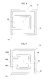
Figures 6 to 10 show various possible implementation solutions for electrical contact pads for a component according toFigure 2 . - It will be appreciated that, for better clarity of illustration, the parts visible in the Figures are not to be considered necessarily drawn to scale.
- In the following description, numerous specific details are given to provide a thorough understanding of one or more exemplary embodiments. The embodiments may be practiced without one or several specific details, or with other methods, components, materials, etc. In other instances, well-known structures, materials, or operations are not shown or described in detail to avoid obscuring various aspects of the embodiments. Reference throughout this specification to "one embodiment" or "an embodiment" means that a particular feature, structure, or characteristic described in connection with the embodiment is included in at least one embodiment. Thus, the possible appearances of the phrases "in one embodiment" or "in an embodiment" in various places throughout this specification are not necessarily all referring to the same embodiment. Furthermore, particular features, structures, or characteristics may be combined in any suitable manner in one or more embodiments, and/or may be associated to the embodiments in a different way from what is shown herein, so that e.g. a feature herein exemplified in connection to a Figure may be applied to one or more embodiments exemplified in a different Figure.
- Specifically, a given feature exemplified herein with reference to an embodiment shown in one of the annexed Figures may be applied to an embodiment shown in any other Figure.
- The headings provided herein are for convenience only, and therefore do not interpret the extent of protection or meaning of the embodiments.
-
Figure 1 shows anelectronic component 10 adapted to be mounted onto a mounting board 12 (see for exampleFigures 4 and 5 ) for example a PCB (Printed Circuit Board). -
Electronic component 10 may be for example a solid-state light radiation source, e.g. a LED light radiation source, such as a power LED. - Such an electronic component may comprise a so-called
package 14, e.g. a ceramic package, which is provided on the underside with pads enabling the mounting ofcomponent 10 onto a board 12, e.g. an IMS (Insulated Metal Substrate) board, by ensuring the electrical contact thereof with supply circuits (which are not visible in the Figures). - According to a conventional solution, shown in
Figure 1 , component 10 (specifically the back side thereof, which will face mounting board 12) may comprise: - two electrical contact pads (in the following we will use this term, which is widely used in the related technology), of an electrically conductive material, e.g. a metal, which are respectively an
anode 16 and acathode 18, and - a
pad 20 of a thermally conductive material, having a heat dissipation function. - Such a
component 10 may be mounted onto a board 12 (e.g. a PCB of the IMS type) by resorting to a layout of mounting contacts formed via known techniques onto the surface of board 12, comprising e.g. a material such as copper, so as to be both electrically and thermally conductive. These contacts define land areas which are adapted to cooperate withpads electronic component 10. - To this end, in order to perform the mounting (with an electrical and heat dissipating mechanical connection), solder pastes may be used which are adapted to be interposed between each pad and a corresponding land area.
- As schematically shown by a dotted line in
Figure 1 , anode and cathodeelectrical contact pads thermal contact pads 20, may be seen as being distributed over the whole back surface of component 10 (the face which will be mounted onto board 12). Such a soldering area includes a central portion CA surrounded by a peripheral or outer portion PA. - In the conventional solution as shown in
Figure 1 : -
thermal contact pad 20 extends over both central portion CA and peripheral portion PA, and -
anode 16 andcathode 18 contact pads extend over peripheral portion PA only, along the sides of the package (which may have a square or rectangular shape) practically over the whole length of the respective side. - It has been ascertained that the creep strain caused by thermal cycles onto the solder joints of the pads grows as the distance from central portion CA increases, and reaches the highest level at the package corners, i.e. at the ends of
anode pad 16 andcathode pad 18. These areas are most subject to crack initiation, which may propagate towards the more central areas, which in themselves are less sensitive to cracks. - One or more embodiments as exemplified in
Figure 2 and in the following figures aim at overcoming such a drawback. - One or more embodiments may be applied to an
electronic component 10 as exemplified inFigure 2 , i.e. for example to a solid-state lighting source wherein, mounted in apackage 14, e.g. a ceramic package, there is provided aLED radiation source 22 with possible associatedoptics 24. - For the rest, in
Figure 2 and the following Figures, the parts and elements which are identical or similar to those previously described with reference toFigure 1 (e.g. component 10, board 12,package 14,contacts - In one or more embodiments as exemplified in
Figure 2 and the following Figures, an arrangement may be provided having at least one first electrical contact pad located in central portion CA of the soldering area, and at least one second electrical contact pad located in peripheral portion PA. - One or more embodiments may omit thermal contact pads such as
pad 20 ofFigure 1 , while conferring the thermal dissipation function only toanode 16 andcathode 18, as they may consist of a material (e.g. a metal) being both electrically and thermally conductive. - For example, in
Figure 3 (which may be considered, in the same way asFigures 6 to 10 , as an ideal plan view ofcomponent 10 viewed from the back side, i.e. the side opposed to the front side visible inFigure 2 ),anode pad 16 andcathode pad 18 are distributed practically over the whole soldering area (and therefore both on central portion CA and on peripheral portion PA), so as to perform, in addition to the electrical contact function, an action of thermal dissipation as well, without the need to provide athermal contact pad 20. - For example, in one or more embodiments, in the absence of thermal contact pads such as
pad 20 visible inFigure 1 ,anode 16 andcathode 18 electrical contact pads may occupy a portion of the soldering area amounting to at least 50% of such soldering area, preferably to at least 70% of the soldering area, and most preferably to at least 90% of the soldering area, comprising central portion CA and peripheral portion PA. - For example, in one or more embodiments as exemplified in
Figure 3 ,anode 16 andcathode 18 electrical contact pads are "split" into two arrays according to a e.g. 4x4 matrix, which may be centred around central portion CA of the soldering area and may comprise: - four pads, respectively
anode pads 16a andcathode pads 18a, arranged in central portion CA of the soldering area, and - further twelve pads, respectively
anode pads 16b andcathode pads 18b, arranged in peripheral portion PA. - Of course, neither the square shape nor the number of rows and columns of the matrix, i.e. the number of pads in the exemplified arrays, are in themselves compulsory features. In one or more embodiments, as a matter of fact, it is possible to adopt rectangular matrix arrangements or non-matrix arrays, e.g. circular or polygonal arrays, possibly comprising a different number of pads.
- One or more embodiments as exemplified in
Figure 3 may therefore envisage at least one first electrical contact pad (16a or 18a) arranged in central portion CA of the soldering area, and at least one secondelectrical contact pad - In one or more embodiments, as exemplified in
Figure 3 , such a result may be achieved by each array, i.e. respectively the anode array (pad pad first pad second pad - In one or more embodiments, the electrical connection between the pads of the respective arrays (i.e. the
anode array cathode array interconnect layer 26, which is arranged on the front side ofpackage 14 of device 10: seeFigure 2 . - As previously stated, the creep strain due to thermal cycles may grow as a function of the distance from the centre of component 10 (portion CA) and therefore have peak levels at the corners of
package 14. These may correspond to the outer corners of bothpad arrays Figure 3 , with the consequent possible crack initiation at such corner portions. The splitting of electrical contact pads intomultiple elements more layers 26 on the front side of component 10), the various pads are physically separated from one another. -
Figures 4 and 5 exemplify possible mounting options of adevice 10 havingelectrical contact pads Figure 3 . -
Figure 4 exemplifies the possibility of using solder pastes which are applied (according to known criteria) onto board 12. - For example, on board 12 there may be formed electrically conductive lines ("tracks"), respectively an
anode track 260 and acathode track 280, on which there may be applied, for example by silk-screen printing with asolder mask 56, individual solder pastes 360, 380 on corresponding land areas, eachsolder paste electrical contact pad - In one or more embodiments, such a result may be obtained either by splitting land areas into respective elements, on each of which a corresponding solder mask is applied, or by using a solder mask which is split into various distinct portions, so as to have respective window portions at each land area, or by using both solutions combined, i.e. by employing both land areas split into several portions and several separate portions of masking window.
- Whatever the solution adopted, distinct solder pastes 360, 380 may be implemented, having a distribution corresponding to
elements -
Figure 6 and the following Figures exemplify embodiments which employ the same principle of having electrical contact (respectively anode and cathode) pads which also perform thermal dissipation, with a consequent elimination ofthermal contact pad 20 adopted in conventional solutions such as depicted inFigure 1 . - The solution moreover comprises:
- (at least) one first electrical contact pad, e.g. a cathode, denoted as 18 in
Figure 6 and located, at least substantially, in central portion CA of the soldering area, - (at least) one second electrical contact pad, e.g. an anode, denoted as 16 in
Figure 6 and having a C-shape or horseshoe shape, so as to embrace the firstelectrical contact pad 18, the second electrical contact pad being located in peripheral portion PA of the soldering area. - In this respect it will be appreciated that the identification of "central"
pad 18 as the cathode pad and of "peripheral"pad 16 as the anode pad is merely exemplary, because the function of both pads might be reversed. -
Figure 7 shows one or more embodiments whereincentral contact pad 18 shows aradial extension 1800 extending towards peripheral portion PA with a width which is shorter than the width of the portion ofcentral pad 18 located at central portion CA. Moreover, the side branches of the C-shape or the horseshoe shape ofperipheral contact pad 16 havedistal portions 1600 facing inwards the horseshoe shape, so as to extend towardsradial extension 1800 ofcentral contact pad 18. - In comparison with the embodiments exemplified in
Figure 6 , one or more embodiments as exemplified inFigure 7 show the feature of having aperipheral pad 16 with an area extending further than the area ofperipheral pad 16 exemplified inFigure 6 , so as to makepad 16 even more resistant to cracking stresses which may arise in peripheral portion PA ofcomponent 10. - For the rest, it will be appreciated that the surface size (area) of
electrical contact pads -
Figure 8 exemplifies one or more embodiments wherein the criteria described with reference to the embodiments exemplified inFigures 6 and 7 are applied by keeping the C-shape or horseshoe shape of "peripheral"contact pad 16, which is however split into two individually formed pads, in turn C-shaped or horseshoe-shaped, respectively aninternal pad 160a and anexternal pad 160b. - As in the case of the
various contact pads Figure 3 , the electrical contact betweenpads circuit layer 26 provided on the front side of package 14 (see for exampleFigure 2 ). - The embodiments exemplified in
Figures 6 and8 aim at increasing the size (e.g. the extension area) of the "peripheral"electrical contact pad 16, which is more exposed to thermal cycle strains adapted to cause cracks in the solder joint. Moreover, the possibility is given to obtain a smaller size of centralelectrical contact pad 18, which is less subjected to such strains because it is located (at least mainly) at central portion CA. In one or more embodiments, as exemplified inFigure 7 , this criterion may be further developed by increasing the size (surface area) of peripheralelectrical contact pad 16 with respect to the size of centralelectrical contact pad 18. - One or more embodiments as exemplified in
Figure 8 may associate, to the size increase of peripheralelectrical contact pad 16, the solution of splitting such a pad, more sensitive to thermal stresses, into at least two elements (the criterion exemplified referring to the pair ofpads inner element 160a, which is physically separated fromelement 160b (the electrical connection being provided e.g. by short-circuit layer 26 on the front side of package 14). -
Figure 9 exemplifies the possibility of extending such a splitting criterion to the central electrical contact pad as well, by physically separating aportion 180b thereof which is not located in central portion CA (and which therefore is potentially more sensitive to cracks) fromportion 180a which is wholly arranged in central portion CA, i.e. which is less sensitive to cracks. In this case, too, the electrical connection between bothpads circuit layer 26 on the front side ofpackage 14. - As previously stated, the possible splitting into two elements both of peripheral pad 16 (
Figures 8 and 9 ) and of central pad 18 (Figure 9 ) may be extended to a higher number of elements. -
Figure 10 exemplifies the possibility of achieving a distribution of electrical contact pads which is substantially similar to what is shown inFigure 3 as regards the geometry of both pad arrays on the back side of component 10 (i.e. a matrix which may be centred around central portion CA of the soldering area), but with different electrical contact arrangements (which again are adapted to be obtained with a short-circuit layer 26 on the front side of package 14). - In one or more embodiments, as exemplified in
Figure 10 , there may be provided: - a first electrical contact array (e.g. a cathode array) comprising four
pads 18a arranged in central portion CA of the soldering area, and twopads 18b arranged in peripheral portion PA, and - a second C-shaped or horseshoe-shaped array of electrical contact pads (e.g. an anode array) surrounding
first pad 18 and comprising an array of tenpads 160 which are all arranged in peripheral portion PA of the soldering area. - One or more embodiments as exemplified in
Figure 10 aim at a size increase of the peripheral electrical contact (pad) 160 which is most exposed to the strains deriving from thermal cycles, combined with the criterion of splitting both electrical contacts, anode and cathode, into a plurality of pads, which are electrically connected to each other, e.g. through alayer 26, but which are physically separated from each other, so as to counter the crack propagation. - In the same way, in the embodiments as exemplified in
Figure 10 , neither the square shape nor the number of rows and columns in the matrix, i.e. the number of pad in the exemplified arrays, are in themselves mandatory features. As a matter of fact, in one or more embodiments there may be provided, for example, either matrix arrangements with rectangular shape, or non-matrix arrays which may be circular, polygonal etc., possibly comprising a different number of pads. - Of course, without prejudice to the basic principles, the details and the embodiments may vary, even appreciably, with respect to what has been described herein by way of non-limiting example only, without departing from the extent of protection.
- The extent of protection is defined by the annexed claims.
Claims (10)
- An electronic component (10) having electrical contact pads (16, 18) for soldering onto a mounting board (12), said electrical contact pads (16, 18) arranged over a soldering area having a central portion (CA) and a peripheral portion (PA) surrounding said central portion (CA), wherein said electrical contact pads (16, 18) include:- at least one first electrical contact pad (16a, 18a; 18; 180a; 18a) at said central portion (CA) of the soldering area, and- at least one second electrical contact pad (16b, 18b; 16; 160a, 160b; 160) at said peripheral portion (PA) of the soldering area.
- The electronic component of claim 1, wherein said contact pads (16, 18) occupy at least 50%, preferably at least 70% and still preferably at least 90% of said soldering area.
- The electronic component of claim 1 or claim 2, wherein said electrical contact pads include a first (16a, 16b) and a second (18a, 18b) array of electrical contact pads, wherein each said array of electrical contact pads includes at least one first electrical contact pad (16a, 18a) at said central portion (CA) of the soldering area, and at least one second electrical contact pad (16b, 18b) at said peripheral portion (PA) of the soldering area.
- The electronic component of any of the previous claims, including a matrix of electrical contact pads (16a, 16b, 18a, 18b; 160, 18a, 18b), preferably centraled about said central portion (CA) of the soldering area.
- The electronic component of any of the previous claims, wherein said at least one second electrical contact pad (16; 160a, 160b; 160) is horseshoe-shaped and embraces said at least one first electrical contact pad (18; 180a, 180b; 18a, 18b).
- The electronic component of claim 5, wherein said at least one first electrical contact pad (18) at said central portion (CA) of the soldering area includes a radial extension (1800) extending over said peripheral portion (PA) of the soldering area and said at least one horseshoe-shaped second electrical contact (16) includes distal portions (1600) extending towards said radial extension (1800) of said at least one first electrical contact pad (18).
- The electronic component of claim 5 or claim 6, wherein at least one of said at least one first electrical contact pad and said at least one second electrical contact pad includes a plurality of electrical contact pads (160a, 160b; 180a, 180b; 18a, 18b; 160).
- The electronic component of any of claims 5 to 7 wherein said at least one first electrical contact pad and said at least one second electrical contact pad are a cathode contact pad (18; 180a, 180b; 18a, 18b) and an anode contact pad (16; 160a, 160b; 160), respectively.
- The electronic component of any of the previous claims, wherein the electronic component (10) includes a solid state light radiation source (22), preferably a LED light radiation source.
- A method of mounting an electronic component onto a mounting board (12) by means of electrical contact pads (16, 18) arranged over a soldering area having a central portion (CA) and a peripheral portion (PA) surrounding said central portion (CA), the method including:- providing at least one first electrical contact pad (16a, 18a; 18; 180a; 18a) at said central portion (CA) of the soldering area, and- providing at least one second electrical contact pad (16b, 18b; 16; 160a, 160b; 160) at said peripheral portion (PA) of the soldering area.
Applications Claiming Priority (1)
| Application Number | Priority Date | Filing Date | Title |
|---|---|---|---|
| ITTO20140942 | 2014-11-12 |
Publications (2)
| Publication Number | Publication Date |
|---|---|
| EP3030059A1 true EP3030059A1 (en) | 2016-06-08 |
| EP3030059B1 EP3030059B1 (en) | 2018-08-15 |
Family
ID=52101514
Family Applications (1)
| Application Number | Title | Priority Date | Filing Date |
|---|---|---|---|
| EP15192592.2A Not-in-force EP3030059B1 (en) | 2014-11-12 | 2015-11-02 | An electronic component and corresponding mounting method |
Country Status (2)
| Country | Link |
|---|---|
| US (1) | US10371357B2 (en) |
| EP (1) | EP3030059B1 (en) |
Families Citing this family (5)
| Publication number | Priority date | Publication date | Assignee | Title |
|---|---|---|---|---|
| JP6284277B2 (en) * | 2015-04-15 | 2018-02-28 | ミネベアミツミ株式会社 | Surface lighting device |
| US10566512B2 (en) * | 2015-12-02 | 2020-02-18 | Lumileds Llc | LED metal pad configuration for optimized thermal resistance |
| CN115529714A (en) * | 2021-06-25 | 2022-12-27 | 全亿大科技(佛山)有限公司 | Circuit board and manufacturing method |
| US12400944B2 (en) | 2022-01-03 | 2025-08-26 | Mediatek Inc. | Board-level pad pattern for multi-row QFN packages |
| US12532758B2 (en) * | 2022-01-03 | 2026-01-20 | Mediatek Inc. | Board-level pad pattern for multi-row QFN packages |
Citations (3)
| Publication number | Priority date | Publication date | Assignee | Title |
|---|---|---|---|---|
| US20070235748A1 (en) * | 2003-01-30 | 2007-10-11 | Tetsushi Tamura | Lighting device having a lighting unit with an optical semiconductor bare chip mounted on printed wiring board |
| US20140146505A1 (en) * | 2012-11-27 | 2014-05-29 | Omnivision Technologies, Inc. | Ball grid array and land grid array having modified footprint |
| US20140217456A1 (en) * | 2013-02-05 | 2014-08-07 | Samsung Electronics Co., Ltd. | Electronic apparatus |
-
2015
- 2015-11-02 EP EP15192592.2A patent/EP3030059B1/en not_active Not-in-force
- 2015-11-11 US US14/937,981 patent/US10371357B2/en active Active
Patent Citations (3)
| Publication number | Priority date | Publication date | Assignee | Title |
|---|---|---|---|---|
| US20070235748A1 (en) * | 2003-01-30 | 2007-10-11 | Tetsushi Tamura | Lighting device having a lighting unit with an optical semiconductor bare chip mounted on printed wiring board |
| US20140146505A1 (en) * | 2012-11-27 | 2014-05-29 | Omnivision Technologies, Inc. | Ball grid array and land grid array having modified footprint |
| US20140217456A1 (en) * | 2013-02-05 | 2014-08-07 | Samsung Electronics Co., Ltd. | Electronic apparatus |
Also Published As
| Publication number | Publication date |
|---|---|
| EP3030059B1 (en) | 2018-08-15 |
| US10371357B2 (en) | 2019-08-06 |
| US20160131340A1 (en) | 2016-05-12 |
Similar Documents
| Publication | Publication Date | Title |
|---|---|---|
| EP3030059B1 (en) | An electronic component and corresponding mounting method | |
| US20040184272A1 (en) | Substrate for light-emitting diode (LED) mounting including heat dissipation structures, and lighting assembly including same | |
| JP5132404B2 (en) | Semiconductor light emitting device | |
| US9125322B2 (en) | Through-hole mounting system with heat sinking elements clamped to one another against insulating body | |
| KR101130137B1 (en) | Light emitting diode module | |
| TW200939527A (en) | Light-emitting module and manufacturing method thereof | |
| US8937375B2 (en) | Substrate structure, semiconductor device array and semiconductor device having the same | |
| TWI714679B (en) | Led metal pad configuration for optimized thermal resistance, solder reliability, and smt processing yields | |
| RU2008108713A (en) | MOUNTING PANEL FOR ELECTRONIC COMPONENT | |
| JP4547781B2 (en) | Method for manufacturing multiple chip resistors | |
| CN105594078A (en) | Optoelectronic component, optoelectronic device and method for producing optoelectronic device | |
| RU2721101C2 (en) | Island holder for light-emitting device | |
| KR101115403B1 (en) | Light emitting apparatus | |
| US9086193B2 (en) | Lighting device having optical element carrying electrical contacts | |
| KR20190003701A (en) | Heat blocking assembly, an LED device having the same, and a method of manufacturing the heat assembly | |
| KR200484643Y1 (en) | Linkage structure of multi pcb | |
| KR101055297B1 (en) | Manufacturing method of metal printed circuit board with improved heat dissipation | |
| JP6447116B2 (en) | LED element substrate and LED display device | |
| WO2016104616A1 (en) | Led-mounted module and led display device | |
| EP3131370B1 (en) | Printed circuit board and light-emitting device including same | |
| KR102105566B1 (en) | Integrated metal printed circuit board | |
| KR20150077208A (en) | Semiconductor device package, light diode package and optical module including the same | |
| JP2013038359A (en) | Semiconductor device and manufacturing method of semiconductor device | |
| CN210928114U (en) | Heat dissipation type light multilayer circuit board | |
| CN210928117U (en) | Anti-corrosion printed circuit board structure |
Legal Events
| Date | Code | Title | Description |
|---|---|---|---|
| PUAI | Public reference made under article 153(3) epc to a published international application that has entered the european phase |
Free format text: ORIGINAL CODE: 0009012 |
|
| AK | Designated contracting states |
Kind code of ref document: A1 Designated state(s): AL AT BE BG CH CY CZ DE DK EE ES FI FR GB GR HR HU IE IS IT LI LT LU LV MC MK MT NL NO PL PT RO RS SE SI SK SM TR |
|
| AX | Request for extension of the european patent |
Extension state: BA ME |
|
| 17P | Request for examination filed |
Effective date: 20161013 |
|
| RBV | Designated contracting states (corrected) |
Designated state(s): AL AT BE BG CH CY CZ DE DK EE ES FI FR GB GR HR HU IE IS IT LI LT LU LV MC MK MT NL NO PL PT RO RS SE SI SK SM TR |
|
| 17Q | First examination report despatched |
Effective date: 20180104 |
|
| GRAP | Despatch of communication of intention to grant a patent |
Free format text: ORIGINAL CODE: EPIDOSNIGR1 |
|
| RIC1 | Information provided on ipc code assigned before grant |
Ipc: H05K 3/34 20060101ALN20180406BHEP Ipc: H01L 33/64 20100101ALI20180406BHEP Ipc: H01L 33/62 20100101ALN20180406BHEP Ipc: H05K 1/11 20060101AFI20180406BHEP |
|
| INTG | Intention to grant announced |
Effective date: 20180504 |
|
| RIN1 | Information on inventor provided before grant (corrected) |
Inventor name: GRIFFONI, ALESSIO Inventor name: ZANON, FRANCO |
|
| GRAS | Grant fee paid |
Free format text: ORIGINAL CODE: EPIDOSNIGR3 |
|
| GRAA | (expected) grant |
Free format text: ORIGINAL CODE: 0009210 |
|
| AK | Designated contracting states |
Kind code of ref document: B1 Designated state(s): AL AT BE BG CH CY CZ DE DK EE ES FI FR GB GR HR HU IE IS IT LI LT LU LV MC MK MT NL NO PL PT RO RS SE SI SK SM TR |
|
| REG | Reference to a national code |
Ref country code: CH Ref legal event code: EP Ref country code: GB Ref legal event code: FG4D Ref country code: AT Ref legal event code: REF Ref document number: 1031319 Country of ref document: AT Kind code of ref document: T Effective date: 20180815 |
|
| REG | Reference to a national code |
Ref country code: IE Ref legal event code: FG4D |
|
| REG | Reference to a national code |
Ref country code: DE Ref legal event code: R096 Ref document number: 602015014710 Country of ref document: DE |
|
| REG | Reference to a national code |
Ref country code: NL Ref legal event code: MP Effective date: 20180815 |
|
| REG | Reference to a national code |
Ref country code: LT Ref legal event code: MG4D |
|
| REG | Reference to a national code |
Ref country code: AT Ref legal event code: MK05 Ref document number: 1031319 Country of ref document: AT Kind code of ref document: T Effective date: 20180815 |
|
| PG25 | Lapsed in a contracting state [announced via postgrant information from national office to epo] |
Ref country code: FI Free format text: LAPSE BECAUSE OF FAILURE TO SUBMIT A TRANSLATION OF THE DESCRIPTION OR TO PAY THE FEE WITHIN THE PRESCRIBED TIME-LIMIT Effective date: 20180815 Ref country code: GR Free format text: LAPSE BECAUSE OF FAILURE TO SUBMIT A TRANSLATION OF THE DESCRIPTION OR TO PAY THE FEE WITHIN THE PRESCRIBED TIME-LIMIT Effective date: 20181116 Ref country code: SE Free format text: LAPSE BECAUSE OF FAILURE TO SUBMIT A TRANSLATION OF THE DESCRIPTION OR TO PAY THE FEE WITHIN THE PRESCRIBED TIME-LIMIT Effective date: 20180815 Ref country code: RS Free format text: LAPSE BECAUSE OF FAILURE TO SUBMIT A TRANSLATION OF THE DESCRIPTION OR TO PAY THE FEE WITHIN THE PRESCRIBED TIME-LIMIT Effective date: 20180815 Ref country code: IS Free format text: LAPSE BECAUSE OF FAILURE TO SUBMIT A TRANSLATION OF THE DESCRIPTION OR TO PAY THE FEE WITHIN THE PRESCRIBED TIME-LIMIT Effective date: 20181215 Ref country code: AT Free format text: LAPSE BECAUSE OF FAILURE TO SUBMIT A TRANSLATION OF THE DESCRIPTION OR TO PAY THE FEE WITHIN THE PRESCRIBED TIME-LIMIT Effective date: 20180815 Ref country code: LT Free format text: LAPSE BECAUSE OF FAILURE TO SUBMIT A TRANSLATION OF THE DESCRIPTION OR TO PAY THE FEE WITHIN THE PRESCRIBED TIME-LIMIT Effective date: 20180815 Ref country code: NO Free format text: LAPSE BECAUSE OF FAILURE TO SUBMIT A TRANSLATION OF THE DESCRIPTION OR TO PAY THE FEE WITHIN THE PRESCRIBED TIME-LIMIT Effective date: 20181115 Ref country code: BG Free format text: LAPSE BECAUSE OF FAILURE TO SUBMIT A TRANSLATION OF THE DESCRIPTION OR TO PAY THE FEE WITHIN THE PRESCRIBED TIME-LIMIT Effective date: 20181115 Ref country code: NL Free format text: LAPSE BECAUSE OF FAILURE TO SUBMIT A TRANSLATION OF THE DESCRIPTION OR TO PAY THE FEE WITHIN THE PRESCRIBED TIME-LIMIT Effective date: 20180815 |
|
| PG25 | Lapsed in a contracting state [announced via postgrant information from national office to epo] |
Ref country code: AL Free format text: LAPSE BECAUSE OF FAILURE TO SUBMIT A TRANSLATION OF THE DESCRIPTION OR TO PAY THE FEE WITHIN THE PRESCRIBED TIME-LIMIT Effective date: 20180815 Ref country code: HR Free format text: LAPSE BECAUSE OF FAILURE TO SUBMIT A TRANSLATION OF THE DESCRIPTION OR TO PAY THE FEE WITHIN THE PRESCRIBED TIME-LIMIT Effective date: 20180815 Ref country code: LV Free format text: LAPSE BECAUSE OF FAILURE TO SUBMIT A TRANSLATION OF THE DESCRIPTION OR TO PAY THE FEE WITHIN THE PRESCRIBED TIME-LIMIT Effective date: 20180815 |
|
| PG25 | Lapsed in a contracting state [announced via postgrant information from national office to epo] |
Ref country code: PL Free format text: LAPSE BECAUSE OF FAILURE TO SUBMIT A TRANSLATION OF THE DESCRIPTION OR TO PAY THE FEE WITHIN THE PRESCRIBED TIME-LIMIT Effective date: 20180815 Ref country code: EE Free format text: LAPSE BECAUSE OF FAILURE TO SUBMIT A TRANSLATION OF THE DESCRIPTION OR TO PAY THE FEE WITHIN THE PRESCRIBED TIME-LIMIT Effective date: 20180815 Ref country code: ES Free format text: LAPSE BECAUSE OF FAILURE TO SUBMIT A TRANSLATION OF THE DESCRIPTION OR TO PAY THE FEE WITHIN THE PRESCRIBED TIME-LIMIT Effective date: 20180815 Ref country code: CZ Free format text: LAPSE BECAUSE OF FAILURE TO SUBMIT A TRANSLATION OF THE DESCRIPTION OR TO PAY THE FEE WITHIN THE PRESCRIBED TIME-LIMIT Effective date: 20180815 Ref country code: IT Free format text: LAPSE BECAUSE OF FAILURE TO SUBMIT A TRANSLATION OF THE DESCRIPTION OR TO PAY THE FEE WITHIN THE PRESCRIBED TIME-LIMIT Effective date: 20180815 Ref country code: RO Free format text: LAPSE BECAUSE OF FAILURE TO SUBMIT A TRANSLATION OF THE DESCRIPTION OR TO PAY THE FEE WITHIN THE PRESCRIBED TIME-LIMIT Effective date: 20180815 |
|
| REG | Reference to a national code |
Ref country code: DE Ref legal event code: R097 Ref document number: 602015014710 Country of ref document: DE |
|
| PG25 | Lapsed in a contracting state [announced via postgrant information from national office to epo] |
Ref country code: SM Free format text: LAPSE BECAUSE OF FAILURE TO SUBMIT A TRANSLATION OF THE DESCRIPTION OR TO PAY THE FEE WITHIN THE PRESCRIBED TIME-LIMIT Effective date: 20180815 Ref country code: SK Free format text: LAPSE BECAUSE OF FAILURE TO SUBMIT A TRANSLATION OF THE DESCRIPTION OR TO PAY THE FEE WITHIN THE PRESCRIBED TIME-LIMIT Effective date: 20180815 Ref country code: DK Free format text: LAPSE BECAUSE OF FAILURE TO SUBMIT A TRANSLATION OF THE DESCRIPTION OR TO PAY THE FEE WITHIN THE PRESCRIBED TIME-LIMIT Effective date: 20180815 |
|
| PLBE | No opposition filed within time limit |
Free format text: ORIGINAL CODE: 0009261 |
|
| STAA | Information on the status of an ep patent application or granted ep patent |
Free format text: STATUS: NO OPPOSITION FILED WITHIN TIME LIMIT |
|
| REG | Reference to a national code |
Ref country code: CH Ref legal event code: PL |
|
| 26N | No opposition filed |
Effective date: 20190516 |
|
| PG25 | Lapsed in a contracting state [announced via postgrant information from national office to epo] |
Ref country code: LU Free format text: LAPSE BECAUSE OF NON-PAYMENT OF DUE FEES Effective date: 20181102 Ref country code: MC Free format text: LAPSE BECAUSE OF FAILURE TO SUBMIT A TRANSLATION OF THE DESCRIPTION OR TO PAY THE FEE WITHIN THE PRESCRIBED TIME-LIMIT Effective date: 20180815 |
|
| REG | Reference to a national code |
Ref country code: BE Ref legal event code: MM Effective date: 20181130 |
|
| REG | Reference to a national code |
Ref country code: IE Ref legal event code: MM4A |
|
| PG25 | Lapsed in a contracting state [announced via postgrant information from national office to epo] |
Ref country code: SI Free format text: LAPSE BECAUSE OF FAILURE TO SUBMIT A TRANSLATION OF THE DESCRIPTION OR TO PAY THE FEE WITHIN THE PRESCRIBED TIME-LIMIT Effective date: 20180815 Ref country code: LI Free format text: LAPSE BECAUSE OF NON-PAYMENT OF DUE FEES Effective date: 20181130 Ref country code: CH Free format text: LAPSE BECAUSE OF NON-PAYMENT OF DUE FEES Effective date: 20181130 |
|
| PG25 | Lapsed in a contracting state [announced via postgrant information from national office to epo] |
Ref country code: FR Free format text: LAPSE BECAUSE OF NON-PAYMENT OF DUE FEES Effective date: 20181130 Ref country code: IE Free format text: LAPSE BECAUSE OF NON-PAYMENT OF DUE FEES Effective date: 20181102 |
|
| PG25 | Lapsed in a contracting state [announced via postgrant information from national office to epo] |
Ref country code: BE Free format text: LAPSE BECAUSE OF NON-PAYMENT OF DUE FEES Effective date: 20181130 |
|
| PG25 | Lapsed in a contracting state [announced via postgrant information from national office to epo] |
Ref country code: MT Free format text: LAPSE BECAUSE OF NON-PAYMENT OF DUE FEES Effective date: 20181102 |
|
| PG25 | Lapsed in a contracting state [announced via postgrant information from national office to epo] |
Ref country code: TR Free format text: LAPSE BECAUSE OF FAILURE TO SUBMIT A TRANSLATION OF THE DESCRIPTION OR TO PAY THE FEE WITHIN THE PRESCRIBED TIME-LIMIT Effective date: 20180815 |
|
| PG25 | Lapsed in a contracting state [announced via postgrant information from national office to epo] |
Ref country code: PT Free format text: LAPSE BECAUSE OF FAILURE TO SUBMIT A TRANSLATION OF THE DESCRIPTION OR TO PAY THE FEE WITHIN THE PRESCRIBED TIME-LIMIT Effective date: 20180815 |
|
| PG25 | Lapsed in a contracting state [announced via postgrant information from national office to epo] |
Ref country code: HU Free format text: LAPSE BECAUSE OF FAILURE TO SUBMIT A TRANSLATION OF THE DESCRIPTION OR TO PAY THE FEE WITHIN THE PRESCRIBED TIME-LIMIT; INVALID AB INITIO Effective date: 20151102 Ref country code: CY Free format text: LAPSE BECAUSE OF FAILURE TO SUBMIT A TRANSLATION OF THE DESCRIPTION OR TO PAY THE FEE WITHIN THE PRESCRIBED TIME-LIMIT Effective date: 20180815 Ref country code: MK Free format text: LAPSE BECAUSE OF NON-PAYMENT OF DUE FEES Effective date: 20180815 |
|
| GBPC | Gb: european patent ceased through non-payment of renewal fee |
Effective date: 20191102 |
|
| PG25 | Lapsed in a contracting state [announced via postgrant information from national office to epo] |
Ref country code: GB Free format text: LAPSE BECAUSE OF NON-PAYMENT OF DUE FEES Effective date: 20191102 |
|
| REG | Reference to a national code |
Ref country code: DE Ref legal event code: R081 Ref document number: 602015014710 Country of ref document: DE Owner name: OPTOTRONIC GMBH, DE Free format text: FORMER OWNER: OSRAM GMBH, 80807 MUENCHEN, DE Ref country code: DE Ref legal event code: R081 Ref document number: 602015014710 Country of ref document: DE Owner name: INVENTRONICS GMBH, DE Free format text: FORMER OWNER: OSRAM GMBH, 80807 MUENCHEN, DE |
|
| PGFP | Annual fee paid to national office [announced via postgrant information from national office to epo] |
Ref country code: DE Payment date: 20231120 Year of fee payment: 9 |
|
| REG | Reference to a national code |
Ref country code: DE Ref legal event code: R081 Ref document number: 602015014710 Country of ref document: DE Owner name: INVENTRONICS GMBH, DE Free format text: FORMER OWNER: OPTOTRONIC GMBH, 85748 GARCHING, DE |
|
| REG | Reference to a national code |
Ref country code: DE Ref legal event code: R119 Ref document number: 602015014710 Country of ref document: DE |
|
| PG25 | Lapsed in a contracting state [announced via postgrant information from national office to epo] |
Ref country code: DE Free format text: LAPSE BECAUSE OF NON-PAYMENT OF DUE FEES Effective date: 20250603 |