EP3029726A1 - Semiconductor device and method for manufacturing same - Google Patents
Semiconductor device and method for manufacturing same Download PDFInfo
- Publication number
- EP3029726A1 EP3029726A1 EP15764791.8A EP15764791A EP3029726A1 EP 3029726 A1 EP3029726 A1 EP 3029726A1 EP 15764791 A EP15764791 A EP 15764791A EP 3029726 A1 EP3029726 A1 EP 3029726A1
- Authority
- EP
- European Patent Office
- Prior art keywords
- terminal
- protrusion
- semiconductor device
- face
- sidewall
- Prior art date
- Legal status (The legal status is an assumption and is not a legal conclusion. Google has not performed a legal analysis and makes no representation as to the accuracy of the status listed.)
- Granted
Links
Images







Classifications
-
- H—ELECTRICITY
- H10—SEMICONDUCTOR DEVICES; ELECTRIC SOLID-STATE DEVICES NOT OTHERWISE PROVIDED FOR
- H10W—GENERIC PACKAGES, INTERCONNECTIONS, CONNECTORS OR OTHER CONSTRUCTIONAL DETAILS OF DEVICES COVERED BY CLASS H10
- H10W76/00—Containers; Fillings or auxiliary members therefor; Seals
- H10W76/10—Containers or parts thereof
- H10W76/12—Containers or parts thereof characterised by their shape
- H10W76/15—Containers comprising an insulating or insulated base
- H10W76/153—Containers comprising an insulating or insulated base having interconnections in passages through the insulating or insulated base
-
- H—ELECTRICITY
- H10—SEMICONDUCTOR DEVICES; ELECTRIC SOLID-STATE DEVICES NOT OTHERWISE PROVIDED FOR
- H10W—GENERIC PACKAGES, INTERCONNECTIONS, CONNECTORS OR OTHER CONSTRUCTIONAL DETAILS OF DEVICES COVERED BY CLASS H10
- H10W40/00—Arrangements for thermal protection or thermal control
- H10W40/10—Arrangements for heating
-
- H—ELECTRICITY
- H10—SEMICONDUCTOR DEVICES; ELECTRIC SOLID-STATE DEVICES NOT OTHERWISE PROVIDED FOR
- H10W—GENERIC PACKAGES, INTERCONNECTIONS, CONNECTORS OR OTHER CONSTRUCTIONAL DETAILS OF DEVICES COVERED BY CLASS H10
- H10W70/00—Package substrates; Interposers; Redistribution layers [RDL]
- H10W70/60—Insulating or insulated package substrates; Interposers; Redistribution layers
- H10W70/62—Insulating or insulated package substrates; Interposers; Redistribution layers characterised by their interconnections
- H10W70/65—Shapes or dispositions of interconnections
-
- H—ELECTRICITY
- H10—SEMICONDUCTOR DEVICES; ELECTRIC SOLID-STATE DEVICES NOT OTHERWISE PROVIDED FOR
- H10W—GENERIC PACKAGES, INTERCONNECTIONS, CONNECTORS OR OTHER CONSTRUCTIONAL DETAILS OF DEVICES COVERED BY CLASS H10
- H10W72/00—Interconnections or connectors in packages
- H10W72/071—Connecting or disconnecting
-
- H—ELECTRICITY
- H10—SEMICONDUCTOR DEVICES; ELECTRIC SOLID-STATE DEVICES NOT OTHERWISE PROVIDED FOR
- H10W—GENERIC PACKAGES, INTERCONNECTIONS, CONNECTORS OR OTHER CONSTRUCTIONAL DETAILS OF DEVICES COVERED BY CLASS H10
- H10W76/00—Containers; Fillings or auxiliary members therefor; Seals
- H10W76/01—Manufacture or treatment
-
- H—ELECTRICITY
- H10—SEMICONDUCTOR DEVICES; ELECTRIC SOLID-STATE DEVICES NOT OTHERWISE PROVIDED FOR
- H10W—GENERIC PACKAGES, INTERCONNECTIONS, CONNECTORS OR OTHER CONSTRUCTIONAL DETAILS OF DEVICES COVERED BY CLASS H10
- H10W76/00—Containers; Fillings or auxiliary members therefor; Seals
- H10W76/10—Containers or parts thereof
- H10W76/12—Containers or parts thereof characterised by their shape
- H10W76/15—Containers comprising an insulating or insulated base
-
- H—ELECTRICITY
- H10—SEMICONDUCTOR DEVICES; ELECTRIC SOLID-STATE DEVICES NOT OTHERWISE PROVIDED FOR
- H10W—GENERIC PACKAGES, INTERCONNECTIONS, CONNECTORS OR OTHER CONSTRUCTIONAL DETAILS OF DEVICES COVERED BY CLASS H10
- H10W76/00—Containers; Fillings or auxiliary members therefor; Seals
- H10W76/40—Fillings or auxiliary members in containers, e.g. centering rings
- H10W76/42—Fillings
-
- H—ELECTRICITY
- H10—SEMICONDUCTOR DEVICES; ELECTRIC SOLID-STATE DEVICES NOT OTHERWISE PROVIDED FOR
- H10W—GENERIC PACKAGES, INTERCONNECTIONS, CONNECTORS OR OTHER CONSTRUCTIONAL DETAILS OF DEVICES COVERED BY CLASS H10
- H10W90/00—Package configurations
Definitions
- the present invention relates to a semiconductor device such as a power semiconductor module for use in electric power conversion or the like and a method for manufacturing the same.
- Fig. 11 is a structural view of a main part of a conventional power semiconductor module 500.
- a main terminal 53 and a control terminal 54 that are independent terminals are bonded to a circuit substrate 52 securely bonded on a heat-dissipating base 51, by soldering or welding.
- the circuit substrate 52 is covered with a resin case 55.
- the resin case 55 there are formed opening portions 56 and 57, through which tip portions of the main terminal 53 and the control terminal 54 are exposed outwardly from the resin case 55.
- the independent terminals are terminals that are not insert-molded in the resin case 55.
- a semiconductor device of a first aspect of the present invention has the following characteristics.
- the positioning component is secured in the groove hole.
- the terminal passes through the through hole toward the main surface side from the opening portion side.
- the trunk portion of the terminal is pressed by the inclined protrusion portion in a sidewall direction to be sandwiched between the inclined protrusion portion and the sidewall, and also the trunk portion is supported by the first corner portion or the second corner portion.
- the second end portion of the terminal protrudes from the main surface of the case body.
- the trunk portion of the terminal is pressed and bent by the inclined protrusion portion of the positioning component in the sidewall direction of the groove hole to be sandwiched between the inclined protrusion portion and the sidewall, so that the second end portion of the terminal is located with high accuracy with respect to the case body.
- a method for manufacturing a semiconductor device of a second aspect of the present invention has the following characteristics.
- a circuit substrate, a case body, and a positioning component are prepared, and a semiconductor device is manufactured by steps including a first step and a second step.
- a terminal including a first end potion, a trunk portion, and a second end portion in this order is secured to the circuit substrate.
- the first end portion of the terminal is secured to the circuit substrate.
- the case body includes a main surface and an opening portion on a side opposing the main surface, and also includes a groove hole on the main surface side.
- the groove hole includes a first corner portion, a sidewall, and a second corner portion that are located toward the opening portion from the main surface.
- the first corner portion is located on a main surface side of the groove hole, and the second corner portion is located on an opening portion side thereof, respectively.
- the positioning component includes a first side face, a second side face opposing the first side face, a front end face positioned between the first side face and the second side face, and a back end face opposing the front end face.
- an inclined protrusion portion that becomes thicker toward the back end face from the front end face is formed on the first side face.
- the circuit substrate is housed in the opening portion so that the second end portion of the terminal passes through the through hole toward the main surface side from the opening portion side of the case body.
- the positioning component is inserted into the groove hole, and secured in the groove hole so that, while bending by being pressed by the inclined protrusion portion in the sidewall direction, the trunk portion of the terminal is sandwiched between the inclined protrusion portion and the sidewall and supported by the first corner portion or the second corner portion.
- the trunk portion of the terminal is bent by being pressed by the inclined protrusion portion in the sidewall direction of the groove hole and is sandwiched between the inclined protrusion portion and the sidewall, so that the second end portion of the terminal is located with high accuracy with respect to the case body.
- a semiconductor device in which a terminal is positioned with high accuracy. Additionally, there can be provided a method for manufacturing a semiconductor device, which allows highly accurate positioning of a terminal.
- Figs. 1 are illustrative views showing a structure of a main part of a semiconductor device according to a first embodiment.
- Fig. 1(a) is a plan view when a semiconductor device 100 according to the first embodiment is seen from a main surface 1s side.
- Fig. 1(b) is a side view taken along line Ib-Ib of Fig. 1(a).
- Fig. 1(c) is a front view of a main terminal 43 when seen from an arrow A direction of Fig. 1(a) .
- Fig. 1(d) is a sectional view showing in detail a section B surrounded by a rectangular frame in Fig. 1(b) .
- the semiconductor device 100 is a power semiconductor module such as, for example, an IGBT module.
- the semiconductor device 100 includes a control terminal 13, a circuit substrate 42, a resin case 1 as a case body, and a resin block 21 as a positioning component.
- the semiconductor device 100 can further include a heat-dissipating base 41, a nut case 45, and a main terminal 43.
- the main terminal 43 is exposed outside the resin case 1 from a top surface of the resin case 1, i.e., an opening portion 44 of the main surface 1s side. Additionally, the main terminal 43 is secured by the nut case 45, as illustrated, but may be secured by other means.
- the main terminal 43 has an inverted U shape, and a top part of the main terminal 43, i.e., a bottom part of the letter U is exposed to an outside of the resin case 1 from the opening portion 44 of the top surface side of the resin case 1.
- Two legs 46 (opening end portions of the letter U) of the main terminal 43 are soldered or welded to the circuit substrate 42.
- the nut case 45 is a resin body housing a nut for connecting an external wire to the main terminal 43 and is inserted between the two legs 46 of the main terminal 43 so as to pass through an inside of a U-shaped hole of the main terminal 43 exposed from the opening portion 44 on the top surface side of the resin case 1, thereby securing the main terminal 43.
- Figs. 3 are illustrative view showing a structure of the control terminal 13.
- Fig. 3(a) is a side view of the control terminal 13
- Fig. 3(b) is a top view of the control terminal 13.
- the control terminal 13 includes a first end portion 13a, a trunk portion 13b, and a second end portion 13c in this order.
- the control terminal 13 may include a connecting portion 13d between the first end portion 13a and the trunk portion 13b.
- the first end portion 13a is secured to the circuit substrate 42.
- a first protrusion portion 16 On one of side faces the trunk portion 13b of the control terminal 13 (hereinafter referred to simply as side end faces) 14, there may be provided a first protrusion portion 16, a second protrusion portion 17 spaced apart from the first protrusion portion 16, and a concave valley (concave portion) 18 between the first protrusion portion 16 and the second protrusion portion 17.
- Symbol 15 in Figs. 3 denotes a flat surface of the trunk 13b (hereinafter referred to simply as flat plate surface).
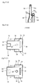
- Figs. 4 are illustrative views showing a structure of the resin block 21 that positions and secures the control terminal 13.
- Fig. 4(a) is a plan view of the resin block 21. In the drawing, arrows, respectively, indicate a longer direction (L) and a shorter direction (S) of the resin block 21.
- Fig. 4(b) is a bottom view of the resin block 21.
- Fig. 4(c) is a side view of the resin block 21.
- the resin block 21 includes, as side faces, a first side face 22r, a second side face 221 opposing the first side face 22r, a front end face 22f positioned between the first side face 22r and the second side face 221, and a back end face 22b opposing the front end face 22f.
- An inclined protrusion portion 23 a that becomes thicker toward the back end face 22b side from the front end face 22f side is formed on at least any one of the first side face 22r and the second side face 221.
- a convex stepped portion 26 may be formed on the side face sides, and a fourth protrusion portion 25 may be formed on a bottom surface 24 side.
- a sixth protrusion portion 26a is formed on a top surface of the convex stepped portion 26.
- a taper is formed so that a height thereof becomes higher toward a rear side from a front side of the resin block 21.
- the rear side of the resin block 21 is a side positioned at the inlet of the opening portion 2 of the side face side of the resin case 1 after assembly of the semiconductor device 100.
- the convex stepped portions 26 are formed on lower sides of the first side face 22r and the second side face 221 at rear end portions of the resin block 21.
- a concave groove 29 is formed at a front end portion 28 of the resin block 21.
- the front end portion 28 is an end portion opposing the front-side sidewall of the opening portion 2 of the resin case 1 after assembly of the semiconductor device 100.
- the resin block 21 has a shape of a letter T, L, or the like in a plan view and is produced by resin molding or the like.
- Figs. 5 show a state in which the resin block 21 is inserted and secured in the opening portion 2 of the resin case 1 of Figs. 2 .
- Fig. 5(a) is a plan view showing locations of the opening portion 2, the control terminal 13, and the resin block 21.
- Fig. 5(b) is a back view when seen from an arrow D direction (rear side) of Fig. 5(a).
- Fig. 5(c) is a sectional view showing a state in which a front end portion 27 of the convex stepped portion 26 of the resin block 21 is fitted in the valley 18 of the control terminal 13.
- Fig. 6 is an enlarged view of a section G of Fig. 5(b) , which is a view illustrating a state of positioning of the control terminal 13.
- the control terminal 13 before inserting the resin block 21, the control terminal 13 is inclined as indicating a position before movement by a dotted line 13e and is in contact with the first corner portion Q1 on the upper end side of the opening portion sidewall 5.
- the trunk portion 13b Along with entry of the resin block 21, when the load P is applied to the trunk portion 13b from the inclined protrusion portion 23a, the trunk portion 13b is bent and closely contacts with the opening portion sidewall 5, and the second end portion 13c rotates about the first corner portion Q1 as a fulcrum in an arrow R direction, so that the control terminal 13 can be positioned with high accuracy with respect to the resin case 1.
- the advancement of the tapered inclined protrusion portion 23a allows an inclined control terminal 13e indicated by the dotted line 13e to be press-contacted and corrected to a perpendicular position, whereby the position of the second end portion 13c of the control terminal 13 is positioned at a normal position, as indicated by a solid line in Fig. 6 .
- the opening portion 2 and the resin block 21 are located so that a position H1 of a bottom surface of the inclined protrusion portion 23a is closer to the main surface 1s side than to a position H2 of a lower end portion Q2 of the opening portion sidewall 5.
- Fig. 14 is an enlarged view of the section G of Fig. 5(b) , which is a view illustrating another example of the state of positioning of the control terminal 13.
- Fig. 6 has shown the example in which the control terminal 13 is inclined outwardly as indicated by the dotted line 13e, whereas Fig. 14 shows an example in which the control terminal 13 is inclined inwardly as indicating a position before movement by the dotted line 13e.
- the first protrusion portion 16, the second protrusion portion 17 spaced apart from the first protrusion portion 16, and the concave valley 18 between the first protrusion portion 16 and the second protrusion portion 17 are provided on the trunk portion 13b.
- the opening portion 2 preferably includes the first concave portion 6 formed in the opening portion sidewall 5 and the beam portion 3 that is located on the bottom surface side thereof and in which the second concave portion 7 is formed.
- the resin block 21 includes the convex stepped portion 26 and the third protrusion portion 23 on the side face sides thereof and includes a fifth protrusion portion 30 on the bottom surface side thereof.
- the front-side end portion 27 of the convex stepped portion 26 of the resin block 21 is fitted into the valley 18 of the control terminal 13.
- the front-side end portion 27 of the convex stepped portion 26 is an end portion opposing a side end face 14 of the control terminal 13 after assembly of the semiconductor device 100.
- tapered sixth protrusion portion 26a may be not provided on the top surface of the stepped portion 26.
- Figs. 15 show modified examples of the opening portion 2 and the resin block 21.
- two through holes 4 have been formed in the single opening portion 2, and each one control terminal 13 has been located in each through hole 4.
- one through hole 4 may be formed in an opening portion 2a, and the control terminal 13 may be located in the through hole 4 and secured by a resin block 21 a including the inclined protrusion portion 23 a only on the first side face 22r, which is shown in Fig. 15(b) .
- control terminal 13 the circuit substrate 42, the resin case 1, and the resin block 21 are prepared.
- the circuit substrate 42 is housed in the opening portion 1op so that the second end portion 13c of the control terminal 13 passes through the through hole 4 toward the main surface 1s side from the opening portion 1op side of the resin case 1.
- the resin block 21 is inserted and secured in the opening portion 2. At this time, while bending by being pressed by the inclined protrusion portion 23 a in a direction of the opening portion sidewall 5, the trunk portion 13b of the control terminal 13 is sandwiched between the inclined protrusion portion 23a and the opening portion sidewall 5 and supported by the first corner portion Q1 or the second corner portion Q2.
- the opening portion 1op of the resin case 1 is bonded to a peripheral edge of the heat-dissipating base 41 so as to house the circuit substrate 42.
- the main terminal 43 is exposed from an upper side of an opening portion 44 of the resin case 1, and the control terminal 13 is caused to pass through the through hole 4 of the opening portion 2.
- the nut case 45 is inserted so as to pass through under the main terminal 43 exposed from the opening portion 44 on the top surface side of the resin case 1.
- the nut case 45 is the resin body housing a nut in a nut receiving portion, and, for example, has a rectangular parallelepiped shape (bar shape). The nut housed in the nut receiving portion can freely move up and down inside the nut receiving portion.
- the main terminal 43 has an inverted U shape, as shown in Fig. 1 (c) , and the nut case 45 is inserted so as to pass through inside the U-shaped hole of the main terminal 43.
- a top part of the main terminal 43 is exposed outside the resin case 1.
- a liquid adhesive agent 47a is dropped (or applied) in the third concave portion 10 formed in the beam portion 3 of the opening portion 2 of the resin case 1.
- the resin block 21 includes the inclined protrusion portion 23a, a part of a force for inserting the resin block 21 is converted into the load P that presses the trunk portion 13b of the control terminal 13 to the opening portion sidewall 5 side.
- the trunk portion 13b is closely contacted with the opening portion sidewall 5 by the load P, and even when the control terminal 13 is inclined, the trunk portion 13b is bent about the first corner portion Q1 as a fulcrum and the second end portion 13c rotates. In this manner, the control terminal 13 can be positioned with high accuracy with respect to the resin case 1.
- the front-side end portion 27 of the convex stepped portion 26 of the resin block 21 may be engaged with the valley 18 of the trunk portion 13b of the control terminal 13.
- the first protrusion portion 16 and the second protrusion portion 17 of the control terminal 13 are supported by the resin block 21, whereby even when an external force such as a compression load or a tensile load is applied to the control terminal 13, the control terminal 13 neither sinks into the resin case 1 nor is pulled outside the resin case 1.
- the convex stepped portion 26 of the resin block 21 may be engaged under the first hood portion 8 of the resin case 1.
- the convex stepped portion 26 is formed on bottom surface sides of the first side face 22r and the second side face 221 of the resin block 21.
- the first hood portion 8 is formed on the main surface 1s side of the opening portion 2.
- the second hood portion 9 formed on the front-side sidewall of the opening portion 2 of the resin case 1 may be engaged with the concave groove 29 formed on the front-side end portion 28 of the resin block 21. Engaging the resin block 21 with the first hood portion 8 and the second hood portion 9 can prevent lifting of the resin block 21 from the resin case 1.
- the top surface and the back surface of the resin block 21 inserted in the opening portion 2 are exposed from the resin case 1.
- Fig. 17 shows a circuit structure of an IGBT module having a 2 in 1 (half bridge) structure.
- the exemplary IGBT module includes input terminals 43p and 43n, an output terminal 43u, gate terminals 13g, and sense terminals 13s.
- the resin block 21 can be used to position the gate terminals 13g and the sense terminals 13s with respect to the resin case 1.
- the power semiconductor module when the power semiconductor module includes the two pairs of gate terminals 13g and the sense terminals 13s, two opening portions 2 are provided in the resin case 1 and the gate terminals 13g and the sense terminals 13s are caused to pass through each through hole 4, thereby allowing positioning by the resin block 21, as in the above-described embodiments.
- an opening portion 2 may be provided for every four terminals and the resin block 21 may be inserted into each thereof to position the terminals.
Landscapes
- Structures Or Materials For Encapsulating Or Coating Semiconductor Devices Or Solid State Devices (AREA)
- Physics & Mathematics (AREA)
- Geometry (AREA)
Abstract
Description
- The present invention relates to a semiconductor device such as a power semiconductor module for use in electric power conversion or the like and a method for manufacturing the same.
- In recent years, integration density has become higher and higher in mounting of power semiconductor modules. Mounting external lead-out terminals of a package on a circuit substrate requires reliability of bonding strengths between the external lead-out terminals such as main terminals and control terminals and the circuit substrate and of bonded portions, and additionally requires positional accuracy relating to locations of the external lead-out terminals.
-
Fig. 11 is a structural view of a main part of a conventionalpower semiconductor module 500. Amain terminal 53 and acontrol terminal 54 that are independent terminals are bonded to acircuit substrate 52 securely bonded on a heat-dissipatingbase 51, by soldering or welding. Thecircuit substrate 52 is covered with aresin case 55. In theresin case 55, there are formedopening portions main terminal 53 and thecontrol terminal 54 are exposed outwardly from theresin case 55. In addition, the independent terminals are terminals that are not insert-molded in theresin case 55. - In the power semiconductor module shown in
Fig. 11 , when a compressive load is applied to thecontrol terminal 54, disadvantages occur where thecontrol terminal 54 sinks into theresin case 55 or thecircuit substrate 52 is cracked in a case in which thecontrol terminal 54 is welded to thecircuit substrate 52 or thecontrol terminal 54 is less deformed. Additionally, application of a tensile load causes a disadvantage where thecontrol terminal 54 is pulled out from theresin base 55. - One technique for solving these troubles is disclosed in
Patent Document 1. -
Figs. 12 are structural views of a main part of aconventional semiconductor device 600 described inPatent Document 1, in whichFig. 12(a) is a top view;Fig. 12(b) is a side view taken along line XIIb-XIIb ofFig. 12(a); Fig. 12(c) is a front view of a main terminal when seen from an arrow A direction ofFig. 12(a) ; andFig. 12(d) is a detailed view of a section B ofFig. 12(b) . The semiconductor device is a power semiconductor module such as an IGBT module. - The
semiconductor device 600 includes aresin case 60, a heat-dissipating base 61, acircuit substrate 62, anut glove 65, amain terminal 63, acontrol terminal 13f, and aresin block 71. Thecircuit substrate 62 is securely bonded on the heat-dissipatingbase 61. Themain terminal 63 and thecontrol terminal 13f that are independent terminals for external leading-out (external connection) are soldered or welded onto thecircuit substrate 62. - The
main terminal 63 and thecontrol terminal 13f are exposed outside theresin case 60 from anopening portion 64 and anopening portion 2a, respectively, on a top surface side of theresin case 60. Additionally, themain terminal 63 is secured to theresin case 60 by thenut glove 65, and thecontrol terminal 13f is secured to theresin case 60 by theresin block 71. Thenut glove 65 is inserted between twolegs 66 of themain terminal 63 so as to pass through an inside of a U-shaped hole of themain terminal 63 exposed from theopening portion 64 on the top surface side of theresin case 60, thereby securing themain terminal 63. - The
control terminal 13f includes an upright portion that is substantially upright with respect to thecircuit substrate 62 and whose one end is exposed outside theresin case 60 and a connecting portion connected to the other end of the upright portion so as to form a substantially L-shape together with the upright portion. A side end face of the upright portion (hereinafter referred to simply as side end face) of thecontrol terminal 13f is provided with first andsecond protrusions concave valley 18a formed by thefirst protrusion portion 16a and thesecond protrusion portion 17a. -
Figs. 13 are views of theresin block 71 that secures thecontrol terminal 13f, in whichFig. 13(a) is a plan view;Fig. 13(b) is a bottom view; andFig. 13(c) is a side view. Athird protrusion portion 73 is formed on bothside faces 72 of theresin block 71, and afourth protrusion portion 75 is formed on abottom surface 74 thereof. Additionally, a convexstepped portion 76 is formed on bothside faces 72, and aconcave groove 79 is formed at a front-side end portion 78 of theresin block 71. Front-side end portions 77 of the convex steppedportions 76 are fitted into thevalley 18a between thefirst protrusion portion 16a and thesecond protrusion portion 17a of thecontrol terminal 13f. - PATENT DOCUMENT 1:
WO 2013/27826 - However, in the
semiconductor device 600, even when thecontrol terminal 13f is secured using theresin block 71, positional accuracy of thecontrol terminal 13f with respect to thesemiconductor device 600 depends on variation in dimensions of respective constituent components and assembly accuracy of theentire semiconductor device 600. Thus, further improvement in positional accuracy has been desired. - It is an object of the present invention to provide a semiconductor device and a method for manufacturing the same that can solve the above-described problem to allow highly accurate positioning of a terminal and a tip portion thereof.
- In order to solve the problem, a semiconductor device of a first aspect of the present invention has the following characteristics.
- The semiconductor device includes a terminal, a circuit substrate, a case body, and a positioning component. The terminal includes a first end portion, a trunk portion, and a second end portion in this order. The first end portion of the terminal is secured to the circuit substrate. The case body includes a main surface and an opening portion that houses the circuit substrate and is on a side opposing the main surface. The case body further includes a groove hole (slot) on the main surface side. The groove hole includes a first corner portion, a sidewall, and a second corner portion that are located toward the opening portion from the main surface, and in which a through hole located adjacent to the second corner portion is formed. The first corner portion is located on a main surface side of the groove hole, and the second corner portion is located on an opening portion side thereof, respectively. The positioning component (locating part) includes a first side face, a second side face opposing the first side face, a front end face positioned between the first side face and the second side face, and a back end face opposing the front end face. In the positioning component, furthermore, an inclined protrusion portion that becomes thicker toward the back end face from the front end face is formed on the first side face.
- The positioning component is secured in the groove hole. The terminal passes through the through hole toward the main surface side from the opening portion side. The trunk portion of the terminal is pressed by the inclined protrusion portion in a sidewall direction to be sandwiched between the inclined protrusion portion and the sidewall, and also the trunk portion is supported by the first corner portion or the second corner portion. The second end portion of the terminal protrudes from the main surface of the case body.
- In this manner, while being supported by the first corner portion of the groove hole on the main surface side or the second corner portion of the groove hole on the opening portion side, the trunk portion of the terminal is pressed and bent by the inclined protrusion portion of the positioning component in the sidewall direction of the groove hole to be sandwiched between the inclined protrusion portion and the sidewall, so that the second end portion of the terminal is located with high accuracy with respect to the case body.
- Additionally, in order to solve the above problem, a method for manufacturing a semiconductor device of a second aspect of the present invention has the following characteristics.
- In the second aspect, a circuit substrate, a case body, and a positioning component are prepared, and a semiconductor device is manufactured by steps including a first step and a second step.
- A terminal including a first end potion, a trunk portion, and a second end portion in this order is secured to the circuit substrate. The first end portion of the terminal is secured to the circuit substrate. The case body includes a main surface and an opening portion on a side opposing the main surface, and also includes a groove hole on the main surface side. The groove hole includes a first corner portion, a sidewall, and a second corner portion that are located toward the opening portion from the main surface. In the groove hole, furthermore, there is formed a through hole located adjacent to the second corner portion. The first corner portion is located on a main surface side of the groove hole, and the second corner portion is located on an opening portion side thereof, respectively. The positioning component includes a first side face, a second side face opposing the first side face, a front end face positioned between the first side face and the second side face, and a back end face opposing the front end face. In the positioning component, furthermore, an inclined protrusion portion that becomes thicker toward the back end face from the front end face is formed on the first side face.
- At the first step, the circuit substrate is housed in the opening portion so that the second end portion of the terminal passes through the through hole toward the main surface side from the opening portion side of the case body. At the second step, the positioning component is inserted into the groove hole, and secured in the groove hole so that, while bending by being pressed by the inclined protrusion portion in the sidewall direction, the trunk portion of the terminal is sandwiched between the inclined protrusion portion and the sidewall and supported by the first corner portion or the second corner portion.
- In this manner, while being supported by the first corner portion or the second corner portion of the groove hole, the trunk portion of the terminal is bent by being pressed by the inclined protrusion portion in the sidewall direction of the groove hole and is sandwiched between the inclined protrusion portion and the sidewall, so that the second end portion of the terminal is located with high accuracy with respect to the case body.
- According to the present invention, there can be provided a semiconductor device in which a terminal is positioned with high accuracy. Additionally, there can be provided a method for manufacturing a semiconductor device, which allows highly accurate positioning of a terminal.
-
-
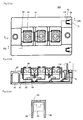
Figs. 1 are illustrative views showing a structure of a main part of a semiconductor device according to a first embodiment of the present invention. -
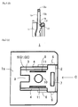
Figs. 2 are illustrative views showing a structure of a main part of a vicinity of an opening portion for a control terminal ofFig. 1 . -
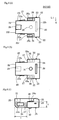
Figs. 3 are illustrative views showing a structure of the control terminal ofFig. 1 . -
Figs. 4 are illustrative views showing a structure of a resin block ofFig. 1 . -
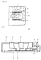
Figs. 5 are illustrative views showing a state in which the control terminal and the resin block are provided in an inserted manner (inserted and installed) in the opening portion for the control terminal ofFig. 2 . -
Fig. 6 is an enlarged view of a section G ofFig. 5(b) , which is a view illustrating a situation of positioning of acontrol terminal 13 by aresin block 21. -
Figs. 7 are illustrative views showing steps for manufacturing a semiconductor device according to a second embodiment of the invention. -
Figs. 8 are illustrative views showing steps for manufacturing the semiconductor device according to the second embodiment of the invention, followingFig. 7 . -
Figs. 9 are illustrative views showing steps for manufacturing the semiconductor device according to the second embodiment of the invention, followingFig. 8 . -
Figs. 10 are illustrative views showing steps for manufacturing the semiconductor device according to the second embodiment of the invention, followingFig. 9 . -
Fig. 11 is a structural view of a main part of a conventional power semiconductor module. -
Figs. 12 are structural views of a main part of aconventional semiconductor device 600 described inPatent Document 1, in which (a) is a plan view; (b) is a side view taken along line XIIb-XIIb ofFig. 12(a); (c) is a front view of a main terminal when seen from an arrow A direction ofFig. 12 (a) ; and(d) is a detailed view of a section B of (b). -
Figs. 13 are views of aconventional resin block 71, in which (a) is a plan view; (b) is a bottom view; and (c) is a side view. -
Fig. 14 is an enlarged view of the section G ofFig. 5(b) showing a modified example of the first embodiment, which is a view illustrating a situation of positioning of thecontrol terminal 13 by theresin block 21. -
Figs. 15 are illustrative views showing a modified example of the opening portion for the control terminal and a modified example of the resin block of the first embodiment. -
Figs. 16 are illustrative views showing main parts of other modified examples of the resin block of the first embodiment. -
Fig. 17 is a view showing a main circuit structure of a power semiconductor module of the first embodiment. - Hereinafter, embodiments of a semiconductor device and a method for manufacturing the semiconductor device according to the present invention will be described with reference to the accompanying drawings.
-
Figs. 1 are illustrative views showing a structure of a main part of a semiconductor device according to a first embodiment.Fig. 1(a) is a plan view when asemiconductor device 100 according to the first embodiment is seen from amain surface 1s side.Fig. 1(b) is a side view taken along line Ib-Ib ofFig. 1(a). Fig. 1(c) is a front view of amain terminal 43 when seen from an arrow A direction ofFig. 1(a) .Fig. 1(d) is a sectional view showing in detail a section B surrounded by a rectangular frame inFig. 1(b) . Thesemiconductor device 100 is a power semiconductor module such as, for example, an IGBT module. - As shown in
Figs. 1 , thesemiconductor device 100 includes acontrol terminal 13, acircuit substrate 42, aresin case 1 as a case body, and aresin block 21 as a positioning component. Thesemiconductor device 100 can further include a heat-dissipatingbase 41, anut case 45, and amain terminal 43. - The
resin case 1 is of a box shape provided with amain surface 1 s and an opening portion 1op on a side opposing themain surface 1s. In the illustrated example, thecircuit substrate 42 is securely bonded onto the heat-dissipatingbase 41. The opening portion 1op of theresin case 1 is bonded to a peripheral edge of the heat-dissipatingbase 41 and houses thecircuit substrate 42. Themain terminal 43 for external leading-out (external connection) and thecontrol terminal 13 are bonded onto thecircuit substrate 42. The method for the bonding is, for example, soldering, brazing, ultrasonic bonding, or welding. As themain terminal 43 and thecontrol terminal 13, examples of independent terminals not insert-molded in theresin case 1 are shown. - In the illustrated example, the
main terminal 43 is exposed outside theresin case 1 from a top surface of theresin case 1, i.e., an openingportion 44 of themain surface 1s side. Additionally, themain terminal 43 is secured by thenut case 45, as illustrated, but may be secured by other means. - As one example, the
main terminal 43 has an inverted U shape, and a top part of themain terminal 43, i.e., a bottom part of the letter U is exposed to an outside of theresin case 1 from the openingportion 44 of the top surface side of theresin case 1. Two legs 46 (opening end portions of the letter U) of themain terminal 43 are soldered or welded to thecircuit substrate 42. Thenut case 45 is a resin body housing a nut for connecting an external wire to themain terminal 43 and is inserted between the twolegs 46 of themain terminal 43 so as to pass through an inside of a U-shaped hole of themain terminal 43 exposed from the openingportion 44 on the top surface side of theresin case 1, thereby securing themain terminal 43. - The
control terminal 13 protrudes from anopening portion 2 as a groove hole (slot) for the control terminal of the top surface (main surface Is) side of theresin case 1 to the outside of theresin case 1. Additionally, thecontrol terminal 13 is secured to theresin case 1 by theresin block 21. Thecontrol terminal 13 is a gate terminal, a sense terminal, or the like. - Next, a further description will be given of structures of the
opening portion 2 of theresin case 1, thecontrol terminal 13, and theresin block 21. -
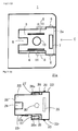
Figs. 2 are illustrative views showing the structure of theopening portion 2 of theresin case 1 ofFigs. 1 .Fig. 2(a) is a partial plan view of theopening portion 2 of theresin case 1 and a portion of a vicinity thereof.Fig. 2(b) is a back view of theresin case 1 whenFig. 2(a) is seen from an arrow C direction. Theresin case 1 includes the top surface (main surface 1s) and side faces adjacent to the main surface. In theresin case 1, theopening portion 2 is formed as a groove hole that straddles over the top surface (main surface Is) and the side faces of theresin case 1. - The
opening portion 2 includes a first corner portion Q1, an openingportion sidewall 5, and a second corner portion Q2 that are located toward the opening portion 1op from themain surface 1s side. The first corner portion Q1 and the second corner portion Q2 can be understood byFig. 6 . A throughhole 4 is located adjacent on the opening portion 1op side of the second corner portion Q2. - The
opening portion 2 can further include the following structure. In the illustrated example, abeam portion 3 is formed on a bottom surface side of theopening portion 2. A convex first hood portion (first stepped portion) 8 protruding toward an inside of theopening portion 2 from thesidewall 5 is formed onmain surface 1s sides of both sides of the openingportion sidewall 5 of theopening portion 2. Furthermore, a convex second hood portion (second stepped portion) 9 protruding toward the inside of theopening portion 2 is formed on a front-side sidewall on the front side of theopening portion 2. The front-side sidewall of theopening portion 2 is a sidewall opposing an inlet of theopening portion 2 on a side face side of theresin case 1. Additionally, on theopening portion sidewall 5, a firstconcave portion 6 is formed toward an outside of theopening portion 2. The firstconcave portion 6 is located at a position spaced apart from thefirst hood portion 8. In thebeam portion 3, a secondconcave portion 7 is formed toward theopening portion 2 side. In addition, the throughhole 4 is formed between thebeam portion 3 and the openingportion sidewall 5. Additionally, in thebeam portion 3, there are formed a thirdconcave portion 10 in which a non-illustrated adhesive agent is dropped (or applied) and aliquid reservoir portion 11 that prevents the adhesive agent from flowing out to thecontrol terminal 13 side. - The
control terminal 13 will be described with reference toFig. 1(d) andFigs. 3 .Fig. 1(d) is a sectional view showing in detail a periphery of thecontrol terminal 13 ofFig. 1(b) . -
Figs. 3 are illustrative view showing a structure of thecontrol terminal 13.Fig. 3(a) is a side view of thecontrol terminal 13, andFig. 3(b) is a top view of thecontrol terminal 13. - The
control terminal 13 includes afirst end portion 13a, atrunk portion 13b, and asecond end portion 13c in this order. Thecontrol terminal 13 may include a connectingportion 13d between thefirst end portion 13a and thetrunk portion 13b. In thecontrol terminal 13, thefirst end portion 13a is secured to thecircuit substrate 42. - In the illustrated example, the
control terminal 13, whosetrunk portion 13b is substantially upright with respect to thecircuit substrate 42, includes thesecond end portion 13c exposed outside theresin case 1 and the connectingportion 13d connected to the other end of thetrunk portion 13b so as to form a substantially L shape together with thetrunk portion 13b. Thefirst end portion 13a is formed at an opposite side of the connectingportion 13d with respect to thetrunk portion 13b. Thefirst end portion 13a is secured to thecircuit substrate 42 by soldering, welding, or the like. Thecontrol terminal 13 is made of, for example, a plate material or a wire material of copper, copper alloy, aluminum, aluminum alloy, or the like. - On one of side faces the
trunk portion 13b of the control terminal 13 (hereinafter referred to simply as side end faces) 14, there may be provided afirst protrusion portion 16, asecond protrusion portion 17 spaced apart from thefirst protrusion portion 16, and a concave valley (concave portion) 18 between thefirst protrusion portion 16 and thesecond protrusion portion 17.Symbol 15 inFigs. 3 denotes a flat surface of thetrunk 13b (hereinafter referred to simply as flat plate surface). -
Figs. 4 are illustrative views showing a structure of theresin block 21 that positions and secures thecontrol terminal 13.Fig. 4(a) is a plan view of theresin block 21. In the drawing, arrows, respectively, indicate a longer direction (L) and a shorter direction (S) of theresin block 21.Fig. 4(b) is a bottom view of theresin block 21.Fig. 4(c) is a side view of theresin block 21. - The
resin block 21 includes, as side faces, afirst side face 22r, asecond side face 221 opposing thefirst side face 22r, afront end face 22f positioned between thefirst side face 22r and thesecond side face 221, and aback end face 22b opposing thefront end face 22f. Aninclined protrusion portion 23 a that becomes thicker toward theback end face 22b side from thefront end face 22f side is formed on at least any one of thefirst side face 22r and thesecond side face 221. - In the
resin block 21, as illustrated, a convex steppedportion 26 may be formed on the side face sides, and afourth protrusion portion 25 may be formed on abottom surface 24 side. Asixth protrusion portion 26a is formed on a top surface of the convex steppedportion 26. On thesixth protrusion portion 26a, a taper is formed so that a height thereof becomes higher toward a rear side from a front side of theresin block 21. The rear side of theresin block 21 is a side positioned at the inlet of theopening portion 2 of the side face side of theresin case 1 after assembly of thesemiconductor device 100. - Forming the taper on the
sixth protrusion portions 26a allows theresin block 21 to be smoothly inserted into theopening portion 2 of theresin case 1. - In the illustrated example, the convex stepped
portions 26 are formed on lower sides of thefirst side face 22r and thesecond side face 221 at rear end portions of theresin block 21. Aconcave groove 29 is formed at afront end portion 28 of theresin block 21. Thefront end portion 28 is an end portion opposing the front-side sidewall of theopening portion 2 of theresin case 1 after assembly of thesemiconductor device 100. In addition, theresin block 21 has a shape of a letter T, L, or the like in a plan view and is produced by resin molding or the like. -
Figs. 5 show a state in which theresin block 21 is inserted and secured in theopening portion 2 of theresin case 1 ofFigs. 2 .Fig. 5(a) is a plan view showing locations of theopening portion 2, thecontrol terminal 13, and theresin block 21.Fig. 5(b) is a back view when seen from an arrow D direction (rear side) ofFig. 5(a). Fig. 5(c) is a sectional view showing a state in which afront end portion 27 of the convex steppedportion 26 of theresin block 21 is fitted in thevalley 18 of thecontrol terminal 13. In addition,Fig. 6 is an enlarged view of a section G ofFig. 5(b) , which is a view illustrating a state of positioning of thecontrol terminal 13. - The
resin block 21 is inserted into theopening portion 2 and secured in theopening portion 2 by fitting or adhesion. Thecontrol terminal 13 passes through the throughhole 4 toward themain surface 1s side from the opening portion 1op of theresin case 1. A part of thetrunk portion 13b of thecontrol terminal 13 is sandwiched between theinclined protrusion portion 23a and the openingportion sidewall 5 while bending by being pressed by theinclined protrusion portion 23a in the direction of the openingportion sidewall 5, and an other part of thetrunk portion 13b is supported by a first corner portion or the second corner portion of the openingportion sidewall 5. Thesecond end portion 13c protrudes from themain surface 1s of theresin case 1. - As shown in
Fig. 6 , when theresin block 21 is inserted into theopening portion 2, theinclined protrusion portion 23a serves as a wedge, whereby aflat plate surface 15 of thetrunk portion 13b is pressed at a load P in a direction substantially perpendicular to an insertion direction. Thetrunk portion 13b of thecontrol terminal 13 is sandwiched between the openingportion sidewall 5 and theinclined protrusion portion 23a. The position of a direction orthogonal to the arrow D direction of the control terminal 13 (a direction orthogonal to theflat plate surface 15 of thecontrol terminal 13 or the shorter direction S) is secured. In the illustrated example, before inserting theresin block 21, thecontrol terminal 13 is inclined as indicating a position before movement by a dottedline 13e and is in contact with the first corner portion Q1 on the upper end side of the openingportion sidewall 5. Along with entry of theresin block 21, when the load P is applied to thetrunk portion 13b from theinclined protrusion portion 23a, thetrunk portion 13b is bent and closely contacts with the openingportion sidewall 5, and thesecond end portion 13c rotates about the first corner portion Q1 as a fulcrum in an arrow R direction, so that thecontrol terminal 13 can be positioned with high accuracy with respect to theresin case 1. In other words, by inserting and installing theresin block 21 in theopening portion 2 of theresin case 1, the advancement of the taperedinclined protrusion portion 23a allows aninclined control terminal 13e indicated by the dottedline 13e to be press-contacted and corrected to a perpendicular position, whereby the position of thesecond end portion 13c of thecontrol terminal 13 is positioned at a normal position, as indicated by a solid line inFig. 6 . - In addition, a width W of the
inclined protrusion portion 23a may be in a range of 0.1 times or more and 0.5 times or less, and preferably 0.2 times or more and 0.5 times or less than a thickness T of theresin block 21. At widths less than 0.2 times, an area of theinclined protrusion portion 23 a with respect to theopening portion sidewall 5 becomes small, which can cause deformation of a vertex of theinclined protrusion portion 23a. Additionally, at widths more than 0.5 times, in a case in which thecontrol terminal 13 formed by molding has a burr, theresin block 21 is hindered by the burr and not smoothly inserted. In addition, although the vertex of theinclined protrusion portion 23a is shown by a sharp edge shape, the vertex thereof may be flattened or a curved surface. In addition, theinclined protrusion portion 23a may be formed on thefirst side face 22r or thesecond side face 221 so that when theresin block 21 is inserted into theopening portion 2, theinclined protrusion portion 23a is positioned closer to the second corner portion Q2 between the first corner portion Q1 and the second corner portion Q2 of the openingportion sidewall 5. In the example shown inFig. 6 , a distance Z between a top surface of theinclined protrusion portion 23 a and a top surface of theresin block 21 may be set to about 1/3 to 1/2 of the thickness T of theresin block 21. Positioning theinclined protrusion portion 23a closer to the second corner portion Q2 increases a length of the close contact between thetrunk portion 13b and the openingportion sidewall 5, thereby facilitating improvement in positional accuracy. Additionally, preferably, theinclined protrusion portion 23a is formed in a hatched range (x, y) ofFig. 4(c) . The x indicates a range of from thefront end face 22f to the front-side end portion 27 of the steppedportion 26, and the y indicates a range of from the bottom surface to an upper end of the steppedportion 26. Locating theinclined protrusion portion 23a in the range (x, y) allows smooth engagement of thevalley 18 of thecontrol terminal 13 and the front-side end portion 27. - More preferably, the
opening portion 2 and theresin block 21 are located so that a position H1 of a bottom surface of theinclined protrusion portion 23a is closer to themain surface 1s side than to a position H2 of a lower end portion Q2 of the openingportion sidewall 5. -
Fig. 14 is an enlarged view of the section G ofFig. 5(b) , which is a view illustrating another example of the state of positioning of thecontrol terminal 13.Fig. 6 has shown the example in which thecontrol terminal 13 is inclined outwardly as indicated by the dottedline 13e, whereasFig. 14 shows an example in which thecontrol terminal 13 is inclined inwardly as indicating a position before movement by the dottedline 13e. - In the example of
Fig. 14 , before inserting theresin block 21, thecontrol terminal 13 is in contact with the second corner portion Q2 on the lower end side of theopening side wall 5. When a load P is applied to thetrunk portion 13b from theinclined protrusion portion 23a, thetrunk portion 13b is bent and closely contacts with the openingportion sidewall 5, and thesecond end portion 13c rotates about the second corner portion Q2 as a fulcrum in an arrow R direction, so that thecontrol terminal 13 can be positioned with high accuracy with respect to theresin case 1. In this example, it is preferable to set a distance H between the H1 and the H2 to 1/5 or more of the thickness T of theresin block 21, since a rotating moment works well when the second corner portion Q2 is the fulcrum. - As described above, in the
control terminal 13, preferably, thefirst protrusion portion 16, thesecond protrusion portion 17 spaced apart from thefirst protrusion portion 16, and theconcave valley 18 between thefirst protrusion portion 16 and thesecond protrusion portion 17 are provided on thetrunk portion 13b. Additionally, theopening portion 2 preferably includes the firstconcave portion 6 formed in theopening portion sidewall 5 and thebeam portion 3 that is located on the bottom surface side thereof and in which the secondconcave portion 7 is formed. Additionally, preferably, theresin block 21 includes the convex steppedportion 26 and thethird protrusion portion 23 on the side face sides thereof and includes afifth protrusion portion 30 on the bottom surface side thereof. - As shown in
Fig. 5(c) , the front-side end portion 27 of the convex steppedportion 26 of theresin block 21 is fitted into thevalley 18 of thecontrol terminal 13. The front-side end portion 27 of the convex steppedportion 26 is an end portion opposing a side end face 14 of thecontrol terminal 13 after assembly of thesemiconductor device 100. - Fitting the front-
side end portion 27 of the convex steppedportion 26 into thevalley 18 allows thecontrol terminal 13 to be supported in the arrow D direction (longer direction L). - In addition, the tapered
sixth protrusion portion 26a may be not provided on the top surface of the steppedportion 26. -
Figs. 15 show modified examples of theopening portion 2 and theresin block 21. In the above-described example, two throughholes 4 have been formed in thesingle opening portion 2, and each onecontrol terminal 13 has been located in each throughhole 4. As shown inFig. 15(a) , one throughhole 4 may be formed in anopening portion 2a, and thecontrol terminal 13 may be located in the throughhole 4 and secured by aresin block 21 a including theinclined protrusion portion 23 a only on thefirst side face 22r, which is shown inFig. 15(b) . - Additionally,
Figs. 16 show modified examples of theinclined protrusion portion 23a. As the shape of theinclined protrusion portion 23a, various shapes can be employed that become gradually thicker toward theback end face 22b from thefront end face 22f side of theresin block 21.Figs. 16(a) to 16(f) show, as examples of such shapes, sections ofinclined protrusion portions 23a to 23a5.Figs. 16(g) to 16(h) are side face views showing modified examples 23a6 and 23a7 of theinclined protrusion portion 23a. Besides theinclined protrusion portions 23a having strip shapes as seen from a side face, the trapezoid inclined protrusion portions 23a6 and 23a7 can be employed. -
Figs. 7 to 10 are illustrative views showing steps of a method for manufacturing a semiconductor device according to a second embodiment. Steps for manufacturing thesemiconductor device 100 shown inFigs. 1 are exemplified. InFigs. 7 to 10 , (a) are sectional views of an entirety of thesemiconductor device 100, and (b) are top-surface enlarged views of a vicinity of thecontrol terminal 13. - As shown in
Figs. 7 to 10 , the steps for manufacturing thesemiconductor device 100 include the following steps: - The
control terminal 13, thecircuit substrate 42, theresin case 1, and theresin block 21 are prepared. - The
control terminal 13 includes thefirst end portion 13a, thetrunk portion 13b, and thesecond end portion 13c in this order. Thefirst end portion 13a of thecontrol terminal 13 is secured to thecircuit substrate 42. Theresin case 1 includes themain surface 1s and the opening portion 1op on the side opposing themain surface 1s. Theresin case 1 further includes the first corner portion Q1, the openingportion sidewall 5, and the second corner portion Q2 that are located toward the opening portion 1op from themain surface 1s. The throughhole 4 is formed adjacent to the second corner portion Q2. Theresin block 21 includes thefirst side face 22r, thesecond side face 221 opposing thefirst side face 22r, thefront end face 22f positioned between thefirst side face 22r and thesecond side face 221, and theback end face 22b opposing thefront end face 22f. In theresin block 21, furthermore, theinclined protrusion portion 23 a that becomes thicker toward theback end face 22b from thefront end face 22f side is formed on thefirst side face 22r. - The
circuit substrate 42 is housed in the opening portion 1op so that thesecond end portion 13c of thecontrol terminal 13 passes through the throughhole 4 toward themain surface 1s side from the opening portion 1op side of theresin case 1. - The
resin block 21 is inserted and secured in theopening portion 2. At this time, while bending by being pressed by theinclined protrusion portion 23 a in a direction of the openingportion sidewall 5, thetrunk portion 13b of thecontrol terminal 13 is sandwiched between theinclined protrusion portion 23a and the openingportion sidewall 5 and supported by the first corner portion Q1 or the second corner portion Q2. - The example of the manufacturing method will be further described. As shown in
Figs. 7 , thecircuit substrate 42, a non-illustrated semiconductor chip, themain terminal 43, and thecontrol terminal 13 are securely bonded to the heat-dissipatingbase 41 by soldering, welding, or the like. The twolegs 46 of themain terminal 43 and thefirst end portion 13a of thecontrol terminal 13, respectively, are secured to thecircuit substrate 42. - Next, the opening portion 1op of the
resin case 1 is bonded to a peripheral edge of the heat-dissipatingbase 41 so as to house thecircuit substrate 42. At this time, themain terminal 43 is exposed from an upper side of anopening portion 44 of theresin case 1, and thecontrol terminal 13 is caused to pass through the throughhole 4 of theopening portion 2. Next, thenut case 45 is inserted so as to pass through under themain terminal 43 exposed from the openingportion 44 on the top surface side of theresin case 1. Thenut case 45 is the resin body housing a nut in a nut receiving portion, and, for example, has a rectangular parallelepiped shape (bar shape). The nut housed in the nut receiving portion can freely move up and down inside the nut receiving portion. - The
main terminal 43 has an inverted U shape, as shown inFig. 1 (c) , and thenut case 45 is inserted so as to pass through inside the U-shaped hole of themain terminal 43. A top part of themain terminal 43 is exposed outside theresin case 1. At the top part of themain terminal 43 exposed outside theresin case 1, there is formed an attachment hole for attachment to an external wire. - Subsequently, as shown in
Figs. 8 , a liquidadhesive agent 47a is dropped (or applied) in the thirdconcave portion 10 formed in thebeam portion 3 of theopening portion 2 of theresin case 1. - Subsequently, as shown in
Figs. 9 , theresin block 21 is inserted into theopening portion 2 of theresin case 1 from the side face side thereof. The insertion direction is a direction parallel to themain surface 1s of theresin case 1. - Since the
resin block 21 includes theinclined protrusion portion 23a, a part of a force for inserting theresin block 21 is converted into the load P that presses thetrunk portion 13b of thecontrol terminal 13 to theopening portion sidewall 5 side. Thetrunk portion 13b is closely contacted with the openingportion sidewall 5 by the load P, and even when thecontrol terminal 13 is inclined, thetrunk portion 13b is bent about the first corner portion Q1 as a fulcrum and thesecond end portion 13c rotates. In this manner, thecontrol terminal 13 can be positioned with high accuracy with respect to theresin case 1. - At this time, the front-
side end portion 27 of the convex steppedportion 26 of theresin block 21 may be engaged with thevalley 18 of thetrunk portion 13b of thecontrol terminal 13. Thefirst protrusion portion 16 and thesecond protrusion portion 17 of thecontrol terminal 13 are supported by theresin block 21, whereby even when an external force such as a compression load or a tensile load is applied to thecontrol terminal 13, thecontrol terminal 13 neither sinks into theresin case 1 nor is pulled outside theresin case 1. - Furthermore, the
third protrusion portion 23 of theresin block 21 may be engaged with the firstconcave portion 6 of theresin case 1, and thefourth protrusion portion 25 may be engaged with the secondconcave portion 7 formed on a bottom portion of theopening portion 2. Engaging the plurality of protrusion portions of theresin block 21 with theopening portion 2 can prevent detachment of theresin block 21 to allow theresin block 21 to be firmly secured to theresin case 1. - Furthermore, the convex stepped
portion 26 of theresin block 21 may be engaged under thefirst hood portion 8 of theresin case 1. The convex steppedportion 26 is formed on bottom surface sides of thefirst side face 22r and thesecond side face 221 of theresin block 21. Thefirst hood portion 8 is formed on themain surface 1s side of theopening portion 2. Additionally, thesecond hood portion 9 formed on the front-side sidewall of theopening portion 2 of theresin case 1 may be engaged with theconcave groove 29 formed on the front-side end portion 28 of theresin block 21. Engaging theresin block 21 with thefirst hood portion 8 and thesecond hood portion 9 can prevent lifting of theresin block 21 from theresin case 1. In addition, the top surface and the back surface of theresin block 21 inserted in theopening portion 2 are exposed from theresin case 1. - Next, as shown in
Figs. 10 , theadhesive agent 47a in liquid form in the thirdconcave portion 10 is solidified into a solidifiedadhesive agent 47b. In order not to allow the adhesive agent in liquid form before solidification to flow out to thecontrol terminal 13 side, a groove as theliquid reservoir portion 11 for the adhesive agent may be provided in thebeam portion 3, as shown inFig. 2(a) . Additionally, the thirdconcave portion 10 may be formed at a center of thebeam portion 3 where the adhesive agent in liquid form is located and may be engaged with thefifth protrusion portion 30 formed on thebottom surface 24 of theresin block 21. In this manner, engaging theresin case 1 with theresin block 21 and at the same time bonding theresin case 1 and theresin block 21 by the adhesive agent allow theresin case 1 and theresin block 21 to be more firmly secured together. In addition, without using theadhesive agent 47a, theresin block 21 may be secured to theresin case 1 only by engagement. - The above-described embodiments can be applied to various power semiconductor modules such as power MOSFET modules and IGBT modules.
Fig. 17 shows a circuit structure of an IGBT module having a 2 in 1 (half bridge) structure. The exemplary IGBT module includesinput terminals output terminal 43u,gate terminals 13g, andsense terminals 13s. Theresin block 21 can be used to position thegate terminals 13g and thesense terminals 13s with respect to theresin case 1. - As described above, when the power semiconductor module includes the two pairs of
gate terminals 13g and thesense terminals 13s, two openingportions 2 are provided in theresin case 1 and thegate terminals 13g and thesense terminals 13s are caused to pass through each throughhole 4, thereby allowing positioning by theresin block 21, as in the above-described embodiments. Alternatively, anopening portion 2 may be provided for every four terminals and theresin block 21 may be inserted into each thereof to position the terminals. - The above-described embodiments can be applied to various power semiconductor modules that are to be mounted with transistor chips such as power MOSFET and IGBT and diode chips such as PN diodes and Schottky barrier diodes produced using monocrystalline silicon substrates. In addition, the embodiments can be applied to power semiconductor modules that are to be mounted with transistor chips and diode chips produced using wide band-gap semiconductors such as silicon carbide (SiC) and gallium nitride (GaN) as a substrate.
-
- 1 Resin case (case body)
- 1s Main surface
- 1op Opening portion
- 2, 2a Opening portion (groove hole)
- 3 Beam portion
- 4 Through hole
- 5 Opening portion sidewall
- 6 First concave portion
- 7 Second concave portion
- 8 First hood portion
- 9 Second hood portion
- 10 Third concave portion
- 11 Liquid reservoir portion
- 13 Control terminal
- 13a First end portion
- 13b Trunk portion
- 13c Second end portion
- 13d Connecting portion
- 14 Side end face
- 15 Flat plate surface
- 16 First protrusion portion
- 17 Second protrusion portion
- 18 Valley
- 21,21a Resin block (positioning component)
- 22r First side face
- 221 Second side face
- 23 Third protrusion portion
- 23a Inclined protrusion portion
- 24 Bottom surface of resin block
- 25 Fourth protrusion portion
- 26 Convex stepped portion of side face of resin block
- 26a Sixth protrusion portion (tapered engaging protrusion)
- 27 Front-side end portion of convex stepped portion
- 28 Front-side end portion of resin block
- 29 Concave groove of resin block
- 30 Fifth protrusion portion
- 41 Heat-dissipating base
- 42 Circuit substrate
- 43 Main terminal
- 44 Opening portion for main terminal
- 45 Nut case
- 46 Leg of main terminal
- 47, 47a Adhesive agent (in liquid form)
- 47b Solidified adhesive agent
Claims (13)
- A semiconductor device comprising:a terminal including a first end portion, a trunk portion, and a second end portion in this order;a circuit substrate to which the first end portion of the terminal is secured;a case body including a main surface, an opening portion that houses the circuit substrate and is on a side opposing the main surface, and a groove hole in which there are formed a first corner portion, a sidewall, and a second corner portion that are located toward the opening portion from the main surface and a through hole located adjacent to the second corner portion; anda positioning component that includes a first side face, a second side face opposing the first side face, a front end face positioned between the first side face and the second side face, and a back end face opposing the front end face and in which an inclined protrusion portion that becomes thicker toward the back end face from the front end face is formed on the first side face,
wherein the positioning component is secured in the groove hole,the terminal passes through the through hole toward the main surface side from the opening portion side, and the trunk portion of the terminal is pressed by the inclined protrusion portion in a direction of the sidewall to be sandwiched between the inclined protrusion portion and the sidewall, the trunk portion being supported by the first corner portion or the second corner portion, andthe second end portion of the terminal protrudes from the main surface of the case body. - The semiconductor device according to claim 1, wherein the second end portion is rotatable about the first corner portion or the second corner portion as a fulcrum, and the trunk portion is pressed against the sidewall, thereby positioning the terminal with respect to the case body.
- The semiconductor device according to claim 1, wherein the inclined protrusion portion has a width of 0.1 to 0.5 times a thickness of the positioning component.
- The semiconductor device according to claim 1, wherein the inclined protrusion portion is formed on the first side face of the positioning component so as to be positioned closer to the second corner portion between the first corner portion and the second corner portion.
- The semiconductor device according to claim 1, wherein, in the terminal, a first protrusion portion, a second protrusion portion spaced apart from the first protrusion portion, and a concave valley between the first protrusion portion and the second protrusion portion are formed on the trunk portion,
the groove hole includes a first concave portion formed on the sidewall and a beam portion that is located on a bottom portion of the groove hole and in which a second concave portion is formed, and
the positioning component includes, on the side face sides, a convex stepped portion fitted in the concave valley of the terminal and a third protrusion portion fitted in the first concave portion and includes, on a bottom surface side, a fourth protrusion portion fitted in the second concave portion. - The semiconductor device according to claim 5, wherein the groove hole includes a hood portion formed on the main surface side of the sidewall and protruding toward an inside of the groove hole,
the positioning component includes a tapered engaging protrusion formed on the main surface side of the convex stepped portion, and
the tapered engaging protrusion is engaged with the hood portion. - The semiconductor device according to claim 5, wherein the bottom surface of the positioning component and the beam portion of the groove hole are secured by an adhesive agent.
- The semiconductor device according to claim 7, wherein a liquid reservoir portion that prevents the adhesive agent in liquid form from flowing out to the terminal side is provided on the beam portion.
- A method for manufacturing a semiconductor device, comprising:preparing a circuit substrate to which a first end portion of a terminal including the first end portion, a trunk portion, and a second end portion in this order is secured and a case body including a main surface, an opening portion on a side opposing the main surface, and a groove hole that includes a first corner portion, a sidewall, and a second corner portion that are located toward the opening portion from the main surface and a through hole located adjacent to the second corner portion;a first step of housing the circuit substrate in the opening portion so that the second end portion of the terminal passes through the through hole toward the main surface side from the opening portion side of the case body;preparing a positioning component that includes a first side face, a second side face opposing the first side face, a front end face positioned between the first side face and the second side face, and a back end face opposing the front end face and in which an inclined protrusion portion that becomes thicker toward the back end face from the front end face is formed on the first side face; anda second step of inserting the positioning component into the groove hole and securing the positioning component in the groove hole so that, while bending by being pressed by the inclined protrusion portion in a direction of the sidewall, the trunk portion of the terminal is sandwiched between the inclined protrusion portion and the sidewall and supported by the first corner portion or the second corner portion.
- The method for manufacturing a semiconductor device according to claim 9, wherein, in the terminal, a first protrusion portion, a second protrusion portion spaced apart from the first protrusion portion, and a concave valley between the first protrusion portion and the second protrusion portion are formed on the trunk portion,
the groove hole includes a first concave portion formed in the sidewall and a beam portion that is located on a bottom portion of the groove hole and in which a second concave portion is formed,
the positioning component further includes a convex stepped potion on the side face sides, a third protrusion portion on the side face sides, and a fourth protrusion portion on a bottom surface side, and
at the second step, the convex stepped portion of the positioning component is fitted into the convex valley of the terminal, and the third protrusion portion and the fourth protrusion portion of the positioning component are fitted into the first concave portion and the second concave portion, respectively, of the groove hole. - The method for manufacturing a semiconductor device according to claim 10, further comprising a step of applying an adhesive agent to the beam portion to secure the positioning component in the groove hole.
- The method for manufacturing a semiconductor device according to claim 11, wherein the second end portion of the terminal is rotated by the inclined protrusion portion of the positioning component until the trunk portion of the terminal contacts with the sidewall of the groove hole of the case body on a deep side in an insertion direction of the positioning component.
- The method for manufacturing a semiconductor device according to claim 10, wherein the groove hole includes a hood portion formed on the main surface side of the sidewall and protruding toward an inside of the groove hole,
the positioning component includes a tapered engaging protrusion formed on the main surface side of the convex stepped portion, and
at the second step, the tapered engaging protrusion is engaged with the hood portion.
Applications Claiming Priority (2)
| Application Number | Priority Date | Filing Date | Title |
|---|---|---|---|
| JP2014055739 | 2014-03-19 | ||
| PCT/JP2015/053474 WO2015141325A1 (en) | 2014-03-19 | 2015-02-09 | Semiconductor device and method for manufacturing same |
Publications (3)
| Publication Number | Publication Date |
|---|---|
| EP3029726A1 true EP3029726A1 (en) | 2016-06-08 |
| EP3029726A4 EP3029726A4 (en) | 2017-04-12 |
| EP3029726B1 EP3029726B1 (en) | 2019-12-11 |
Family
ID=54144305
Family Applications (1)
| Application Number | Title | Priority Date | Filing Date |
|---|---|---|---|
| EP15764791.8A Active EP3029726B1 (en) | 2014-03-19 | 2015-02-09 | Semiconductor device and manufacturing method thereof |
Country Status (5)
| Country | Link |
|---|---|
| US (1) | US9691674B2 (en) |
| EP (1) | EP3029726B1 (en) |
| JP (1) | JP6057016B2 (en) |
| CN (1) | CN105518851B (en) |
| WO (1) | WO2015141325A1 (en) |
Families Citing this family (11)
| Publication number | Priority date | Publication date | Assignee | Title |
|---|---|---|---|---|
| CN106796934B (en) * | 2015-04-10 | 2019-12-10 | 富士电机株式会社 | Semiconductor device with a plurality of semiconductor chips |
| CN107851633B (en) * | 2016-01-12 | 2021-05-18 | 富士电机株式会社 | semiconductor device |
| JP6625044B2 (en) * | 2016-12-28 | 2019-12-25 | 三菱電機株式会社 | Semiconductor device and method of manufacturing the same |
| JP6755197B2 (en) * | 2017-01-19 | 2020-09-16 | 三菱電機株式会社 | Semiconductor devices and their manufacturing methods |
| EP3682475A1 (en) | 2017-09-15 | 2020-07-22 | Finar Module Sagl | Packaging method and joint technology for an electronic device |
| JP7099524B2 (en) * | 2018-06-19 | 2022-07-12 | 富士電機株式会社 | Manufacturing method of semiconductor device and semiconductor device |
| JP7207611B2 (en) * | 2020-06-16 | 2023-01-18 | 富士電機株式会社 | semiconductor module |
| JP7444121B2 (en) * | 2021-03-26 | 2024-03-06 | 横河電機株式会社 | Electronics |
| JP7830884B2 (en) * | 2021-10-18 | 2026-03-17 | 富士電機株式会社 | Semiconductor module |
| JP2023085776A (en) | 2021-12-09 | 2023-06-21 | 富士電機株式会社 | semiconductor module |
| CN116053246A (en) * | 2023-01-06 | 2023-05-02 | 株洲中车时代半导体有限公司 | Semiconductor power modules and power devices |
Family Cites Families (13)
| Publication number | Priority date | Publication date | Assignee | Title |
|---|---|---|---|---|
| JPH056852U (en) * | 1991-07-08 | 1993-01-29 | 三菱電機株式会社 | Semiconductor device |
| JP2560909Y2 (en) | 1991-08-05 | 1998-01-26 | 日本インター株式会社 | Composite semiconductor device |
| WO1994003038A1 (en) | 1992-07-17 | 1994-02-03 | Vlt Corporation | Packaging electrical components |
| EP0884781A3 (en) * | 1997-06-12 | 1999-06-30 | Hitachi, Ltd. | Power semiconductor module |
| DE10232566B4 (en) * | 2001-07-23 | 2015-11-12 | Fuji Electric Co., Ltd. | Semiconductor device |
| JP5479703B2 (en) * | 2008-10-07 | 2014-04-23 | 株式会社東芝 | Semiconductor device and manufacturing method thereof |
| EP2642517B1 (en) * | 2010-11-16 | 2021-12-29 | Fuji Electric Co., Ltd. | Semiconductor device |
| CN103430306B (en) * | 2011-03-16 | 2016-06-29 | 富士电机株式会社 | Semiconductor module and manufacture method thereof |
| DE102011075921B8 (en) * | 2011-05-16 | 2014-08-07 | Infineon Technologies Ag | By means of clamping wedge and counter wedge electrically connectable power semiconductor module and power semiconductor module system with such a power semiconductor module |
| CN103299421B (en) * | 2011-07-28 | 2016-03-16 | 富士电机株式会社 | Semiconductor device and method for manufacturing semiconductor device |
| EP2750187B1 (en) | 2011-08-25 | 2020-01-01 | Fuji Electric Co., Ltd. | Semiconductor device and semiconductor device manufacturing method |
| EP2725610B1 (en) * | 2011-09-28 | 2020-06-03 | Fuji Electric Co., Ltd. | Semiconductor device and method for producing semiconductor device |
| CN103515364A (en) * | 2012-06-29 | 2014-01-15 | 三星电机株式会社 | Power module package and method for manufacturing the same |
-
2015
- 2015-02-09 WO PCT/JP2015/053474 patent/WO2015141325A1/en not_active Ceased
- 2015-02-09 CN CN201580001811.6A patent/CN105518851B/en active Active
- 2015-02-09 JP JP2016508589A patent/JP6057016B2/en active Active
- 2015-02-09 EP EP15764791.8A patent/EP3029726B1/en active Active
- 2015-02-09 US US14/917,453 patent/US9691674B2/en active Active
Also Published As
| Publication number | Publication date |
|---|---|
| EP3029726B1 (en) | 2019-12-11 |
| EP3029726A4 (en) | 2017-04-12 |
| JPWO2015141325A1 (en) | 2017-04-06 |
| JP6057016B2 (en) | 2017-01-11 |
| WO2015141325A1 (en) | 2015-09-24 |
| CN105518851A (en) | 2016-04-20 |
| US20160225685A1 (en) | 2016-08-04 |
| US9691674B2 (en) | 2017-06-27 |
| CN105518851B (en) | 2018-07-03 |
Similar Documents
| Publication | Publication Date | Title |
|---|---|---|
| EP3029726B1 (en) | Semiconductor device and manufacturing method thereof | |
| KR101539250B1 (en) | Thermally enhanced thin semiconductor package | |
| US9171768B2 (en) | Semiconductor device | |
| US20090042337A1 (en) | Method of Manufacturing an Integrated Circuit Module | |
| CN103946976A (en) | Dual-level leadframe and device packaging with flipped ball-bonding surfaces | |
| CN102194806A (en) | Stacked double chip package and its preparation method | |
| KR20110117211A (en) | Semiconductor die package and its manufacturing method | |
| EP2642517A1 (en) | Semiconductor device | |
| EP3761359B1 (en) | A lead frame assembly for a semiconductor device | |
| US9136225B2 (en) | Semiconductor device manufacturing method | |
| KR20180006839A (en) | Semiconductor package with clip alignment notch and related methods | |
| JP7192789B2 (en) | semiconductor equipment | |
| CN104134646A (en) | Lead frame strip with support member | |
| KR101569769B1 (en) | Semiconductor package with clip structure and fabricating method for the same | |
| US20110163432A1 (en) | Semiconductor device and method of manufacturing the same | |
| JP4489791B2 (en) | QFN package | |
| KR101561920B1 (en) | Semiconductor package | |
| US11600547B2 (en) | Semiconductor package with expanded heat spreader | |
| JP4974943B2 (en) | Resin encapsulated semiconductor device | |
| JP4207791B2 (en) | Semiconductor device | |
| JP4556732B2 (en) | Semiconductor device and manufacturing method thereof | |
| US20060170080A1 (en) | Semiconductor device having directly attached heat spreader | |
| US20250273541A1 (en) | Interdigitated cantilever lead frame in chip-on-lead package design | |
| JP4291788B2 (en) | Semiconductor device and manufacturing method thereof | |
| US20260053009A1 (en) | Semiconductor packages and related methods to enable wettable flanks |
Legal Events
| Date | Code | Title | Description |
|---|---|---|---|
| PUAI | Public reference made under article 153(3) epc to a published international application that has entered the european phase |
Free format text: ORIGINAL CODE: 0009012 |
|
| 17P | Request for examination filed |
Effective date: 20160303 |
|
| AK | Designated contracting states |
Kind code of ref document: A1 Designated state(s): AL AT BE BG CH CY CZ DE DK EE ES FI FR GB GR HR HU IE IS IT LI LT LU LV MC MK MT NL NO PL PT RO RS SE SI SK SM TR |
|
| AX | Request for extension of the european patent |
Extension state: BA ME |
|
| REG | Reference to a national code |
Ref country code: DE Ref legal event code: R079 Ref document number: 602015043490 Country of ref document: DE Free format text: PREVIOUS MAIN CLASS: H01L0023040000 Ipc: H01L0025070000 |
|
| A4 | Supplementary search report drawn up and despatched |
Effective date: 20170309 |
|
| RIC1 | Information provided on ipc code assigned before grant |
Ipc: H01L 23/053 20060101ALI20170303BHEP Ipc: H01L 25/07 20060101AFI20170303BHEP Ipc: H01L 25/18 20060101ALI20170303BHEP |
|
| DAX | Request for extension of the european patent (deleted) | ||
| GRAP | Despatch of communication of intention to grant a patent |
Free format text: ORIGINAL CODE: EPIDOSNIGR1 |
|
| STAA | Information on the status of an ep patent application or granted ep patent |
Free format text: STATUS: GRANT OF PATENT IS INTENDED |
|
| INTG | Intention to grant announced |
Effective date: 20190708 |
|
| GRAS | Grant fee paid |
Free format text: ORIGINAL CODE: EPIDOSNIGR3 |
|
| GRAA | (expected) grant |
Free format text: ORIGINAL CODE: 0009210 |
|
| STAA | Information on the status of an ep patent application or granted ep patent |
Free format text: STATUS: THE PATENT HAS BEEN GRANTED |
|
| AK | Designated contracting states |
Kind code of ref document: B1 Designated state(s): AL AT BE BG CH CY CZ DE DK EE ES FI FR GB GR HR HU IE IS IT LI LT LU LV MC MK MT NL NO PL PT RO RS SE SI SK SM TR |
|
| REG | Reference to a national code |
Ref country code: GB Ref legal event code: FG4D |
|
| REG | Reference to a national code |
Ref country code: CH Ref legal event code: EP |
|
| REG | Reference to a national code |
Ref country code: AT Ref legal event code: REF Ref document number: 1213050 Country of ref document: AT Kind code of ref document: T Effective date: 20191215 |
|
| REG | Reference to a national code |
Ref country code: DE Ref legal event code: R096 Ref document number: 602015043490 Country of ref document: DE |
|
| REG | Reference to a national code |
Ref country code: IE Ref legal event code: FG4D |
|
| REG | Reference to a national code |
Ref country code: NL Ref legal event code: MP Effective date: 20191211 |
|
| REG | Reference to a national code |
Ref country code: LT Ref legal event code: MG4D |
|
| PG25 | Lapsed in a contracting state [announced via postgrant information from national office to epo] |
Ref country code: LT Free format text: LAPSE BECAUSE OF FAILURE TO SUBMIT A TRANSLATION OF THE DESCRIPTION OR TO PAY THE FEE WITHIN THE PRESCRIBED TIME-LIMIT Effective date: 20191211 Ref country code: GR Free format text: LAPSE BECAUSE OF FAILURE TO SUBMIT A TRANSLATION OF THE DESCRIPTION OR TO PAY THE FEE WITHIN THE PRESCRIBED TIME-LIMIT Effective date: 20200312 Ref country code: NO Free format text: LAPSE BECAUSE OF FAILURE TO SUBMIT A TRANSLATION OF THE DESCRIPTION OR TO PAY THE FEE WITHIN THE PRESCRIBED TIME-LIMIT Effective date: 20200311 Ref country code: SE Free format text: LAPSE BECAUSE OF FAILURE TO SUBMIT A TRANSLATION OF THE DESCRIPTION OR TO PAY THE FEE WITHIN THE PRESCRIBED TIME-LIMIT Effective date: 20191211 Ref country code: LV Free format text: LAPSE BECAUSE OF FAILURE TO SUBMIT A TRANSLATION OF THE DESCRIPTION OR TO PAY THE FEE WITHIN THE PRESCRIBED TIME-LIMIT Effective date: 20191211 Ref country code: BG Free format text: LAPSE BECAUSE OF FAILURE TO SUBMIT A TRANSLATION OF THE DESCRIPTION OR TO PAY THE FEE WITHIN THE PRESCRIBED TIME-LIMIT Effective date: 20200311 Ref country code: FI Free format text: LAPSE BECAUSE OF FAILURE TO SUBMIT A TRANSLATION OF THE DESCRIPTION OR TO PAY THE FEE WITHIN THE PRESCRIBED TIME-LIMIT Effective date: 20191211 |
|
| PG25 | Lapsed in a contracting state [announced via postgrant information from national office to epo] |
Ref country code: RS Free format text: LAPSE BECAUSE OF FAILURE TO SUBMIT A TRANSLATION OF THE DESCRIPTION OR TO PAY THE FEE WITHIN THE PRESCRIBED TIME-LIMIT Effective date: 20191211 Ref country code: HR Free format text: LAPSE BECAUSE OF FAILURE TO SUBMIT A TRANSLATION OF THE DESCRIPTION OR TO PAY THE FEE WITHIN THE PRESCRIBED TIME-LIMIT Effective date: 20191211 |
|
| PG25 | Lapsed in a contracting state [announced via postgrant information from national office to epo] |
Ref country code: AL Free format text: LAPSE BECAUSE OF FAILURE TO SUBMIT A TRANSLATION OF THE DESCRIPTION OR TO PAY THE FEE WITHIN THE PRESCRIBED TIME-LIMIT Effective date: 20191211 |
|
| PG25 | Lapsed in a contracting state [announced via postgrant information from national office to epo] |
Ref country code: PT Free format text: LAPSE BECAUSE OF FAILURE TO SUBMIT A TRANSLATION OF THE DESCRIPTION OR TO PAY THE FEE WITHIN THE PRESCRIBED TIME-LIMIT Effective date: 20200506 Ref country code: ES Free format text: LAPSE BECAUSE OF FAILURE TO SUBMIT A TRANSLATION OF THE DESCRIPTION OR TO PAY THE FEE WITHIN THE PRESCRIBED TIME-LIMIT Effective date: 20191211 Ref country code: CZ Free format text: LAPSE BECAUSE OF FAILURE TO SUBMIT A TRANSLATION OF THE DESCRIPTION OR TO PAY THE FEE WITHIN THE PRESCRIBED TIME-LIMIT Effective date: 20191211 Ref country code: NL Free format text: LAPSE BECAUSE OF FAILURE TO SUBMIT A TRANSLATION OF THE DESCRIPTION OR TO PAY THE FEE WITHIN THE PRESCRIBED TIME-LIMIT Effective date: 20191211 Ref country code: EE Free format text: LAPSE BECAUSE OF FAILURE TO SUBMIT A TRANSLATION OF THE DESCRIPTION OR TO PAY THE FEE WITHIN THE PRESCRIBED TIME-LIMIT Effective date: 20191211 Ref country code: RO Free format text: LAPSE BECAUSE OF FAILURE TO SUBMIT A TRANSLATION OF THE DESCRIPTION OR TO PAY THE FEE WITHIN THE PRESCRIBED TIME-LIMIT Effective date: 20191211 |
|
| PG25 | Lapsed in a contracting state [announced via postgrant information from national office to epo] |
Ref country code: SM Free format text: LAPSE BECAUSE OF FAILURE TO SUBMIT A TRANSLATION OF THE DESCRIPTION OR TO PAY THE FEE WITHIN THE PRESCRIBED TIME-LIMIT Effective date: 20191211 Ref country code: IS Free format text: LAPSE BECAUSE OF FAILURE TO SUBMIT A TRANSLATION OF THE DESCRIPTION OR TO PAY THE FEE WITHIN THE PRESCRIBED TIME-LIMIT Effective date: 20200411 Ref country code: SK Free format text: LAPSE BECAUSE OF FAILURE TO SUBMIT A TRANSLATION OF THE DESCRIPTION OR TO PAY THE FEE WITHIN THE PRESCRIBED TIME-LIMIT Effective date: 20191211 |
|
| REG | Reference to a national code |
Ref country code: DE Ref legal event code: R097 Ref document number: 602015043490 Country of ref document: DE |
|
| REG | Reference to a national code |
Ref country code: CH Ref legal event code: PL |
|
| REG | Reference to a national code |
Ref country code: AT Ref legal event code: MK05 Ref document number: 1213050 Country of ref document: AT Kind code of ref document: T Effective date: 20191211 |
|
| PLBE | No opposition filed within time limit |
Free format text: ORIGINAL CODE: 0009261 |
|
| STAA | Information on the status of an ep patent application or granted ep patent |
Free format text: STATUS: NO OPPOSITION FILED WITHIN TIME LIMIT |
|
| REG | Reference to a national code |
Ref country code: BE Ref legal event code: MM Effective date: 20200229 |
|
| PG25 | Lapsed in a contracting state [announced via postgrant information from national office to epo] |
Ref country code: LU Free format text: LAPSE BECAUSE OF NON-PAYMENT OF DUE FEES Effective date: 20200209 Ref country code: MC Free format text: LAPSE BECAUSE OF FAILURE TO SUBMIT A TRANSLATION OF THE DESCRIPTION OR TO PAY THE FEE WITHIN THE PRESCRIBED TIME-LIMIT Effective date: 20191211 Ref country code: DK Free format text: LAPSE BECAUSE OF FAILURE TO SUBMIT A TRANSLATION OF THE DESCRIPTION OR TO PAY THE FEE WITHIN THE PRESCRIBED TIME-LIMIT Effective date: 20191211 |
|
| 26N | No opposition filed |
Effective date: 20200914 |
|
| PG25 | Lapsed in a contracting state [announced via postgrant information from national office to epo] |
Ref country code: SI Free format text: LAPSE BECAUSE OF FAILURE TO SUBMIT A TRANSLATION OF THE DESCRIPTION OR TO PAY THE FEE WITHIN THE PRESCRIBED TIME-LIMIT Effective date: 20191211 Ref country code: CH Free format text: LAPSE BECAUSE OF NON-PAYMENT OF DUE FEES Effective date: 20200229 Ref country code: LI Free format text: LAPSE BECAUSE OF NON-PAYMENT OF DUE FEES Effective date: 20200229 Ref country code: AT Free format text: LAPSE BECAUSE OF FAILURE TO SUBMIT A TRANSLATION OF THE DESCRIPTION OR TO PAY THE FEE WITHIN THE PRESCRIBED TIME-LIMIT Effective date: 20191211 |
|
| PG25 | Lapsed in a contracting state [announced via postgrant information from national office to epo] |
Ref country code: IE Free format text: LAPSE BECAUSE OF NON-PAYMENT OF DUE FEES Effective date: 20200209 Ref country code: FR Free format text: LAPSE BECAUSE OF NON-PAYMENT OF DUE FEES Effective date: 20200211 Ref country code: IT Free format text: LAPSE BECAUSE OF FAILURE TO SUBMIT A TRANSLATION OF THE DESCRIPTION OR TO PAY THE FEE WITHIN THE PRESCRIBED TIME-LIMIT Effective date: 20191211 |
|
| PG25 | Lapsed in a contracting state [announced via postgrant information from national office to epo] |
Ref country code: BE Free format text: LAPSE BECAUSE OF NON-PAYMENT OF DUE FEES Effective date: 20200229 Ref country code: PL Free format text: LAPSE BECAUSE OF FAILURE TO SUBMIT A TRANSLATION OF THE DESCRIPTION OR TO PAY THE FEE WITHIN THE PRESCRIBED TIME-LIMIT Effective date: 20191211 |
|
| GBPC | Gb: european patent ceased through non-payment of renewal fee |
Effective date: 20200311 |
|
| PG25 | Lapsed in a contracting state [announced via postgrant information from national office to epo] |
Ref country code: GB Free format text: LAPSE BECAUSE OF NON-PAYMENT OF DUE FEES Effective date: 20200311 |
|
| PG25 | Lapsed in a contracting state [announced via postgrant information from national office to epo] |
Ref country code: TR Free format text: LAPSE BECAUSE OF FAILURE TO SUBMIT A TRANSLATION OF THE DESCRIPTION OR TO PAY THE FEE WITHIN THE PRESCRIBED TIME-LIMIT Effective date: 20191211 Ref country code: MT Free format text: LAPSE BECAUSE OF FAILURE TO SUBMIT A TRANSLATION OF THE DESCRIPTION OR TO PAY THE FEE WITHIN THE PRESCRIBED TIME-LIMIT Effective date: 20191211 Ref country code: CY Free format text: LAPSE BECAUSE OF FAILURE TO SUBMIT A TRANSLATION OF THE DESCRIPTION OR TO PAY THE FEE WITHIN THE PRESCRIBED TIME-LIMIT Effective date: 20191211 |
|
| PG25 | Lapsed in a contracting state [announced via postgrant information from national office to epo] |
Ref country code: MK Free format text: LAPSE BECAUSE OF FAILURE TO SUBMIT A TRANSLATION OF THE DESCRIPTION OR TO PAY THE FEE WITHIN THE PRESCRIBED TIME-LIMIT Effective date: 20191211 |
|
| REG | Reference to a national code |
Ref country code: DE Ref legal event code: R079 Ref document number: 602015043490 Country of ref document: DE Free format text: PREVIOUS MAIN CLASS: H01L0025070000 Ipc: H10D0080200000 |
|
| PGFP | Annual fee paid to national office [announced via postgrant information from national office to epo] |
Ref country code: DE Payment date: 20251230 Year of fee payment: 12 |