EP3029579A2 - Controller with indirect accessible memory - Google Patents
Controller with indirect accessible memory Download PDFInfo
- Publication number
- EP3029579A2 EP3029579A2 EP15202847.8A EP15202847A EP3029579A2 EP 3029579 A2 EP3029579 A2 EP 3029579A2 EP 15202847 A EP15202847 A EP 15202847A EP 3029579 A2 EP3029579 A2 EP 3029579A2
- Authority
- EP
- European Patent Office
- Prior art keywords
- address
- registers
- memory
- register
- serial interface
- Prior art date
- Legal status (The legal status is an assumption and is not a legal conclusion. Google has not performed a legal analysis and makes no representation as to the accuracy of the status listed.)
- Ceased
Links
- 239000000872 buffer Substances 0.000 claims abstract description 74
- 230000006870 function Effects 0.000 claims description 19
- 238000000034 method Methods 0.000 claims description 15
- 230000005540 biological transmission Effects 0.000 claims description 6
- 230000008901 benefit Effects 0.000 description 5
- 239000012464 large buffer Substances 0.000 description 4
- 238000004891 communication Methods 0.000 description 3
- 238000010586 diagram Methods 0.000 description 2
- 230000007246 mechanism Effects 0.000 description 2
- 230000004075 alteration Effects 0.000 description 1
- 230000008878 coupling Effects 0.000 description 1
- 238000010168 coupling process Methods 0.000 description 1
- 238000005859 coupling reaction Methods 0.000 description 1
- 230000001419 dependent effect Effects 0.000 description 1
- 238000013461 design Methods 0.000 description 1
- 238000011156 evaluation Methods 0.000 description 1
- 238000001914 filtration Methods 0.000 description 1
- 238000012432 intermediate storage Methods 0.000 description 1
- 230000004048 modification Effects 0.000 description 1
- 238000012986 modification Methods 0.000 description 1
- 230000002093 peripheral effect Effects 0.000 description 1
Images


Classifications
-
- G—PHYSICS
- G06—COMPUTING; CALCULATING OR COUNTING
- G06F—ELECTRIC DIGITAL DATA PROCESSING
- G06F13/00—Interconnection of, or transfer of information or other signals between, memories, input/output devices or central processing units
- G06F13/14—Handling requests for interconnection or transfer
- G06F13/16—Handling requests for interconnection or transfer for access to memory bus
- G06F13/1668—Details of memory controller
- G06F13/1673—Details of memory controller using buffers
-
- G—PHYSICS
- G06—COMPUTING; CALCULATING OR COUNTING
- G06F—ELECTRIC DIGITAL DATA PROCESSING
- G06F13/00—Interconnection of, or transfer of information or other signals between, memories, input/output devices or central processing units
- G06F13/10—Program control for peripheral devices
- G06F13/12—Program control for peripheral devices using hardware independent of the central processor, e.g. channel or peripheral processor
- G06F13/124—Program control for peripheral devices using hardware independent of the central processor, e.g. channel or peripheral processor where hardware is a sequential transfer control unit, e.g. microprocessor, peripheral processor or state-machine
- G06F13/128—Program control for peripheral devices using hardware independent of the central processor, e.g. channel or peripheral processor where hardware is a sequential transfer control unit, e.g. microprocessor, peripheral processor or state-machine for dedicated transfers to a network
Definitions
- the technical field of the present application relates to controllers with an indirectly accessible memory.
- Ethernet controllers in particular stand alone Ethernet Controllers, are designed to serve as an Ethernet network interface for any type of microprocessor or microcontroller.
- a controller can have a fairly large memory and may include a dedicated interface such as a serial peripheral interface (SPI) bus.
- SPI serial peripheral interface
- such an Ethernet controller may also be integrated in a microcontroller using the SPI bus or any other capable interface connection.
- the controller handles all communication protocols and comprises a large buffer for intermediate storage of incoming and outgoing messages.
- a microcontroller or microprocessor may then communicate and control the Ethernet controller via the interface.
- the stand alone or an integrated Ethernet controller handles coordination of incoming and outgoing data packets as well as packet filtering. It may further comprise an internal direct memory access (DMA) module for fast data throughput and hardware assisted checksum calculation.
- DMA direct memory access
- the communication of an Ethernet controller with a microcontroller or microprocessor can be established interrupt or polling driven.
- the buffer incorporated in this type of controllers is relatively large and, therefore, cannot be directly addressed, due to address size limitations of the communication protocols of the respective interface.
- the buffer is generally accessed through a windowed interface via a set of control registers.
- a set of control registers comprises a register for data to be written or read and at least one pointer register containing the physical read or write address of the buffer.
- This accessing scheme may cause a bottleneck in present Ethernet controllers in particular for operations that often switch between read and write access or between different tasks accessing the Ethernet buffer that make it necessary every time a switch occurs to save the content of the pointer registers.
- This object can be achieved by the controller and method as defined in the independent claims. Further enhancements are characterized in the dependent claims.
- a controller may comprise an interface, a buffer memory, a first set of registers for accessing the buffer memory, a second set of registers independent from the first set of registers for accessing the buffer memory, and a control unit for decoding and executing buffer memory access commands received by the interface to access the buffer memory through either the first or second set of registers.
- the first set of registers may comprise a first read pointer register and a first write pointer register and the second set of registers may comprise a second read pointer register and a second write pointer register.
- the controller may further comprise an auto-increment or auto-decrement unit for incrementing or decrementing the content of at least one register of the first and/or second set of registers.
- the controller may further comprise a wrap around unit for resetting the address stored in at least one pointer register of the first and/or second set of registers to a predefined address.
- the controller may further comprise at least one multiplexer coupled with each pointer register.
- the multiplexer further may receive a direct address signal.
- the controller may further comprise a special function register for defining a split address in the buffer memory splitting the buffer memory into a first segment assigned to the first set of registers and a second segment assigned to the second set of registers.
- the controller may further comprise a plurality of special function registers for defining memory segments in the buffer memory assigned to each set of registers.
- the controller may further comprise at least a third set of registers independent from the first and second set of registers for accessing the buffer memory, wherein the third set of registers comprises a third read pointer register and a third write pointer register.
- the controller may be an Ethernet controller and the packet buffer memory may be coupled with the set of registers and coupled with transmit and receive units of the Ethernet controller.
- an Ethernet controller may comprise a physical layer and a media access control layer, a buffer memory, a physical and media access control layer coupled with the buffer memory, a set of transmit (TX) registers coupled with the buffer memory, comprising a first read pointer register and a first write pointer register, a set of receive (RX) registers coupled with the buffer memory, comprising a second read pointer register and a second write pointer register, a set of user defined registers coupled with the buffer memory, comprising a third read pointer register and a third write pointer register, and a control unit for decoding and executing buffer memory access commands received by an interface to access the buffer memory through either said transmit, receive, or user defined registers.
- TX transmit
- RX receive
- the Ethernet controller may further comprise an auto-increment or auto-decrement unit for incrementing or decrementing the content of any one of the pointer registers.
- the Ethernet controller may further comprise a wrap around unit for resetting the address stored in any one of the pointer registers to a predefined start address.
- the Ethernet controller may further comprise at least one multiplexer coupled with each pointer register.
- the multiplexer further may receive a direct address signal.
- the Ethernet controller may further comprise a special function register for defining a split address in the buffer memory splitting the buffer memory into a first segment assigned to the transmit registers and a second segment assigned to the receive registers.
- the Ethernet controller may further comprise a plurality of special function registers for defining a memory segment for the user defined registers. According to a further embodiment, the Ethernet controller may further comprise a plurality of special function registers for defining memory segments in the buffer memory assigned to each set of registers.
- a method for accessing a memory in a controller through an interface with limited addressing capabilities may comprise the steps of: loading a first address of the memory through the interface into a first address register of a first set of access registers; loading a second address of the memory through the interface into a second address register of a second set of access registers; receiving a first read command through the interface; accessing the memory through the first address register and receiving first data from the first address in the memory; outputting the first data through the interface; receiving a second read command through the interface; accessing the memory through the second address register and receiving second data from the second address in the memory; and outputting the second data through the interface.
- the method may further comprise the step of auto-incrementing or auto-decrementing the first and second address registers after reading the memory.
- the method may further comprise the step of performing an address wrap around function on the first and second address registers after auto-incrementing or auto-decrementing.
- the method may further comprise the steps of: loading a third address of the memory through the interface into a third address register of a third set of access registers; loading a third address of the memory through the interface into a third address register of a third set of access registers; receiving a third read command through the interface; accessing the memory through the third address register and receiving third data from the third address in the memory; and outputting the third data through the interface.
- a method for accessing a memory in a controller through an interface with limited addressing capabilities may comprise the steps of: loading a first address through the interface into a first address register of a first set of access registers; loading a second address through the interface into a second address register of a second set of access registers; receiving a first write command through the interface; receiving first write data through the interface; accessing the memory through the first address register and storing the first data under the first address into the memory; receiving a second write command through the interface; receiving second write data through the interface; and accessing the memory through the second address register and storing the second data under the second address into the memory.
- the method may further comprise the step of auto-incrementing or auto-decrementing the first and second address registers after reading the memory.
- the method may further comprise the step of performing an address wrap around function on the first and second address registers after auto-incrementing or auto-decrementing.
- the method may further comprise the steps of: loading a third address through the interface into a third address register of a third set of access registers; loading a third address through the interface into a third address register of a third set of access registers; receiving a third write command through the interface; receiving third write data through the interface; and accessing the memory through the third address register and storing the third data under the third address into the memory.
- such a stand alone controller or a module which can be integrated into a microcontroller has an interface with limited address capabilities.
- a typical 8 bit serial interface would require a plurality of address transmissions to form a long address capable of addressing every memory location in a large buffer memory.
- direct access through such an interface would form a bottleneck and slow transmissions rates significantly down.
- such modules comprise a windowed access mechanism in which an address register is used to provide for the actual address.
- This address register usually only has to be set once in most applications, such as Ethernet controllers, because the access to such a large buffer is usually sequential. In other words, once a specific memory location has been accessed, the address only needs to be incremented or decremented depending on the writing mechanism to access the next memory location.
- This increment or decrement function can be automatically handled by the controller without the support of the external processor.
- an auto-increment and/or auto-decrement functionality is implemented.
- the microcontroller needs to initiate the address registers once through the serial interface and then only needs to send a read or write command every time access to the buffer is required.
- the respective Ethernet module or controller then answers this command by sending or receiving the respective data from or to the memory, by incrementing or decrementing the pointer register and by waiting for the next command.
- Other commands, such a block read or block write can be implemented which cause the respective controller to transmit a plurality of sequential data, for example, one or more data packets, from or to such a large buffer.
- Fig. 1 shows as an embodiment of a controller a block diagram of a Ethernet controller 100 that can be a stand alone Ethernet controller or an Ethernet controller module integrated, for example, in a microcontroller.
- the Ethernet controller 100 comprises a typical physical layer (PHY) 170 with transmit and receive units TX and RX for transmitting and receiving of the actual analog data over the network.
- This physical layer 170 is coupled with a media access control (MAC) data link layer 150 for implementing the actual Ethernet standard (IEEE 802.3).
- the Mac layer 150 is coupled with a receive unit 135 and a transmit unit 145 which may include respective filter units flow control and host interfaces.
- the Ethernet controller may also include a direct memory access (DMA) controller 140 capable of performing, for example, a checksum evaluation.
- DMA direct memory access
- An arbiter 130 may be implemented to switch coupling between the actual buffer 125 and the modules 120, 135, 140, and 145.
- the control registers 120 are coupled with a bus interface 115 and a serial or parallel interface 105.
- the serial interface can be, for example, a SPI interface or any other suitable inter circuit interface.
- the bus interface 115 may provide for additional interrupt signals to provide for additional control of the Ethernet controller 100.
- the Ethernet controller 100 may be internally controlled by a system control unit 110 which controls the respective units of the Ethernet controller 100.
- System control unit 110 receives commands from the serial or parallel interface 105 and provides for decoding of these commands. The commands can provide for reading and writing of at least some or all registers and for executing functions of the respective controller.
- the system control 110 may provide for the respective control sequences to perform read and write access to the buffer 125 as will be explained in more detail below.
- Clock unit 160 provides for the required Ethernet transmission clock signal.
- Fig. 2 shows certain details of a specific section 200 of another embodiment of any type of controller having a window access memory.
- multiple interfaces for a microcontroller or microprocessor are provided.
- a first interface is provided by SPI interface 210 and a second by parallel interface 220. Both interfaces may be limited in their address capability and therefore require the windowed memory access.
- Both interfaces are coupled with a multiplexer 230 which is controlled by signal 215 which can be supplied externally.
- the device 200 can operate with either a parallel or a serial interface.
- the output of multiplexer 230 is coupled to various control registers and to the input of a further multiplexer 260.
- the various control registers may comprise a set of multiple window access registers 250.
- Such additional control logic 290 can for example provide for auto-increment and/or auto-decrement and wrap around functionality of the pointer registers and, thus, control and manage the boundaries for predefined memory segments in the buffer.
- the read channel and the write channel may have assigned memory segments in the buffer.
- these boundary control 290 can monitor the access address stored in the respective registers and provide for wrap around functionality if a pointer register oversteps a boundary.
- the memory segments can also overlap to allow for enhanced functionalities.
- the output of multiplexer 260 is coupled to the actual buffer 125 and can be optionally also coupled to a control register block 270 comprising a plurality of special function registers. Furthermore, as indicated by block 280, clock and reset logic can be provided.
- the window access registers 250 may include three sets of data/pointer registers. Each data/pointer register set comprises separate read and write pointer registers and may also include a data register or latch. In some embodiments, a data register such as a latch may not be necessary and the data input output may be directly routed to respective data busses of the system. In other embodiments, only two set of registers or more than 3 set of registers can be provided.
- a first set of registers is dedicated to a first channel, for example, the transmit channel TX. It may comprise a data register or latch 310. However, as indicated by the dotted lines, this register may simply represent a memory mapped address within the packet buffer 125 which causes the data to/from the buffer 125 to be transferred from/to the SPI/Parallel interface 210/220.
- Each set of registers comprises a write pointer register 315 and a read pointer register 320.
- the read and write pointer registers 315 and 320 can be coupled with a multiplexer 325 which outputs an address signal 327 fed to a first input of a multiplexer 380.
- the data 310 is received from packet buffer 125.
- a second set of registers is dedicated to a second channel, for example, the receive channel RX. It comprises a write pointer register 335 and a read pointer register 340.
- a data latch 330 can be implemented depending on various design choices.
- the read and write pointer registers 335 and 340 are coupled with a multiplexer 345 which outputs an address signal 347 fed to a second input of multiplexer 380. If implemented, the data latch 330 is coupled with packet buffer 125 for data input/output.
- a third set of registers is dedicated to a third channel, providing for example a user defined access. The set comprises a write pointer register 355 and a read pointer register 360.
- the read and write pointer registers 355 and 360 are coupled with a multiplexer 365 which outputs an address signal 367 fed to a third input of multiplexer 380.
- the data latch 350 can be coupled directly with the data port of packet buffer 125.
- Multiplexer 380 may also have a fourth input for providing a direct address.
- the output signals of multiplexer 380 is used to address buffer 125.
- the output data is provided at the respective packet buffer output.
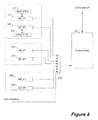
- Fig. 4 shows a second embodiment with a single multiplexer 410.
- Multiplexer 410 has 7 inputs and selects one of these inputs for addressing packet buffer 125.
- Each of the three register sets provides for a write and a read address.
- a direct address can be provided circumventing the indirect addressing provided by the three register sets.
- the data input/output is directly routed to a respective data bus without any intervening latches.
- data latches can be provided individually or for all indirect register sets.
- a read command send by an external processor to the controller causes the system control to execute a sequence of steps to provide the external processor with the requested data.
- the system control uses a designated register set to access the buffer.
- Each register set may have dedicated read and write commands or dedicated memory-mapped addresses.
- a special function register may be used to define which register set is to be used.
- Other commands may cause a block read or packet read which provide for a plurality of data.
- System control unit 110 provides for the respective functionality by a state machine or small controller unit that interprets and executes the defined commands.
- each read or write pointer is usually auto-incremented or auto-decremented.
- the accessing controller must first save the content of at least the pointer registers.
- each read and write register may only access predefined areas of the buffer. For example, the buffer may be segmented into an area for the receiving channel RX and an area for the transmitting channel TX. These areas may not overlap and thus depending on which channel is active a single address pointer register set must be compared to the respective boundaries of that channel.
- the access circuitry for windowed access to the buffer comprises a plurality of independent register sets wherein each set comprises a separate data register and associated read and write pointer registers.
- each register set may comprise an independent control logic for controlling the boundaries.
- a transmit write pointer boundary control unit 317 may be coupled with register 315. This boundary control unit 317 may include auto increment and/or auto-decrement logic as well as compare logic to compare the content of register 315 against a predefined or programmable boundary.
- this control unit 317 can generate an interrupt if a boundary is crossed or can reset the address to a predefined or programmable segment start address, thereby, providing for a wrap around functionality.
- the pointer register 315 could provide the functionality of a first in first out (FIFO) register.
- a separate control unit 322 may be provided for the read pointer register 320. However, each set of registers may only provide for a single boundary control unit that operates on both read and write pointer registers 315 and 320. Even though not shown, similar units can be provided for the read control register set 330-340 and the user defined access register set 350-360.
- Multiplexer 380 is controlled by the interface or system control unit 110 and selects the appropriate outputs to couple the buffer 125 with a single set of control registers.
- Fig. 5 shows an example of predefined or programmable segments.
- buffer 125 may be divided into two main non-overlapping segments A and B.
- the segments can also be defined to overlap.
- a first address 347 points to any address for the receive channel within the predefined boundaries A.
- a single control unit 510 is used to control the registers 335 and 340. This control register can auto-increment or decrement the content of the register after an access to buffer 125 has been completed.
- unit 510 may provide for a boundary check of the respective address and reset the register to a start address of segment A if an increment of the address would cause a cross over into segment B.
- control unit 520 may provide for the same functionality with respect to the transmit channel and registers 315 and 320.
- Special function registers may be provided to define segments A and B, for example, a register may comprise the split address that divides buffer 125 into two segments. However, in other embodiments, the boundaries of these segments can be freely programmed.
- additional special function registers may be provided to define a user defined address segment C as shown in Fig. 4 . This user defined segment may overlap with one or both segments.
- User defined control unit 530 may also provide for similar functionalities as units 510 and 520. Due to the fact that the transmit channel and the read channel as well as a further user defined access comprise separate access registers, the respective control logic can be simplified because only a single boundary address must be compared. Moreover, switches between those channels do not require the necessity of saving the content of these registers, thus, these registers have to be saved only in certain scenarios. This allows for reduced software overhead and avoids any timing problems with respect to these pointer registers.
- register block 515 may indicate the level of unread data in a segment by comparing the address 347 and the respective pointer in unit 135 (See Fig. 1 ).
- a predefined threshold may generate an interrupt to signal a low level of data in buffer 125.
- register DATAHIGH a high level of data can be indicated by register DATAHIGH. Again this register could cause an interrupt if a high threshold level is exceeded indicating to a microcontroller or processor that the buffer has to be read to prevent an overflow.
- Other registers may be provided as indicated by the empty control registers that, for example, comprise certain absolute boundary addresses within a segment that may generate interrupts.
- other special functions associated with the address pointer signals 327, 347, and 367 may be provided.
- buffer 125 may be divided into more than 2 segments.
- Specific packet filters can be assigned in units 135 and 145 (See Fig. 1 ) to provide for respective transmit and receive functionality that is assigned to those segments. For example, each filter may read or write only from an assigned segment. Units 135 and 145 may provide for the same wrap around functionality, thus, creating respective FIFO registers. Further control logic can be provided to prevent overwriting of unread data by comparing the respective address pointers of units 135, 145 and window access registers 250.
- the present invention is not limited to Ethernet controllers but can be applied to any type of stand alone controller or integratable controller having a memory that is indirectly accessed via respective pointer registers.
Abstract
Description
- The technical field of the present application relates to controllers with an indirectly accessible memory.
- Many controller exist, in particular stand alone controllers, that comprise a large memory that is not directly accessible by a processor due to constraints in address size of an associated interface. For example, Ethernet controllers, in particular stand alone Ethernet Controllers, are designed to serve as an Ethernet network interface for any type of microprocessor or microcontroller. Such a controller can have a fairly large memory and may include a dedicated interface such as a serial peripheral interface (SPI) bus. In some embodiments, such an Ethernet controller may also be integrated in a microcontroller using the SPI bus or any other capable interface connection. In case of an Ethernet controller, the controller handles all communication protocols and comprises a large buffer for intermediate storage of incoming and outgoing messages. A microcontroller or microprocessor may then communicate and control the Ethernet controller via the interface. The stand alone or an integrated Ethernet controller handles coordination of incoming and outgoing data packets as well as packet filtering. It may further comprise an internal direct memory access (DMA) module for fast data throughput and hardware assisted checksum calculation. The communication of an Ethernet controller with a microcontroller or microprocessor can be established interrupt or polling driven.
- As stated above, the buffer incorporated in this type of controllers is relatively large and, therefore, cannot be directly addressed, due to address size limitations of the communication protocols of the respective interface. Hence, the buffer is generally accessed through a windowed interface via a set of control registers. Such a set of control registers comprises a register for data to be written or read and at least one pointer register containing the physical read or write address of the buffer. This accessing scheme however may cause a bottleneck in present Ethernet controllers in particular for operations that often switch between read and write access or between different tasks accessing the Ethernet buffer that make it necessary every time a switch occurs to save the content of the pointer registers.
- It is therefore an object of the present invention to provide a controller and a method of operating such a controller that simplifies the access of an processor to the memory of the controller via an interface with limited addressing capabilities. This object can be achieved by the controller and method as defined in the independent claims. Further enhancements are characterized in the dependent claims.
- According to an embodiment, a controller may comprise an interface, a buffer memory, a first set of registers for accessing the buffer memory, a second set of registers independent from the first set of registers for accessing the buffer memory, and a control unit for decoding and executing buffer memory access commands received by the interface to access the buffer memory through either the first or second set of registers.
- According to a further embodiment, the first set of registers may comprise a first read pointer register and a first write pointer register and the second set of registers may comprise a second read pointer register and a second write pointer register. According to a further embodiment, the controller may further comprise an auto-increment or auto-decrement unit for incrementing or decrementing the content of at least one register of the first and/or second set of registers. According to a further embodiment, the controller may further comprise a wrap around unit for resetting the address stored in at least one pointer register of the first and/or second set of registers to a predefined address. According to a further embodiment, the controller may further comprise at least one multiplexer coupled with each pointer register. According to a further embodiment, the multiplexer further may receive a direct address signal. According to a further embodiment, the controller may further comprise a special function register for defining a split address in the buffer memory splitting the buffer memory into a first segment assigned to the first set of registers and a second segment assigned to the second set of registers. According to a further embodiment, the controller may further comprise a plurality of special function registers for defining memory segments in the buffer memory assigned to each set of registers. According to a further embodiment, the controller may further comprise at least a third set of registers independent from the first and second set of registers for accessing the buffer memory, wherein the third set of registers comprises a third read pointer register and a third write pointer register. According to a further embodiment, the controller may be an Ethernet controller and the packet buffer memory may be coupled with the set of registers and coupled with transmit and receive units of the Ethernet controller.
- According to another embodiment, an Ethernet controller may comprise a physical layer and a media access control layer, a buffer memory, a physical and media access control layer coupled with the buffer memory, a set of transmit (TX) registers coupled with the buffer memory, comprising a first read pointer register and a first write pointer register, a set of receive (RX) registers coupled with the buffer memory, comprising a second read pointer register and a second write pointer register, a set of user defined registers coupled with the buffer memory, comprising a third read pointer register and a third write pointer register, and a control unit for decoding and executing buffer memory access commands received by an interface to access the buffer memory through either said transmit, receive, or user defined registers.
- According to a further embodiment, the Ethernet controller may further comprise an auto-increment or auto-decrement unit for incrementing or decrementing the content of any one of the pointer registers. According to a further embodiment, the Ethernet controller may further comprise a wrap around unit for resetting the address stored in any one of the pointer registers to a predefined start address. According to a further embodiment, the Ethernet controller may further comprise at least one multiplexer coupled with each pointer register. According to a further embodiment, the multiplexer further may receive a direct address signal. According to a further embodiment, the Ethernet controller may further comprise a special function register for defining a split address in the buffer memory splitting the buffer memory into a first segment assigned to the transmit registers and a second segment assigned to the receive registers. According to a further embodiment, the Ethernet controller may further comprise a plurality of special function registers for defining a memory segment for the user defined registers. According to a further embodiment, the Ethernet controller may further comprise a plurality of special function registers for defining memory segments in the buffer memory assigned to each set of registers.
- According to yet another embodiment, a method for accessing a memory in a controller through an interface with limited addressing capabilities, may comprise the steps of: loading a first address of the memory through the interface into a first address register of a first set of access registers; loading a second address of the memory through the interface into a second address register of a second set of access registers; receiving a first read command through the interface; accessing the memory through the first address register and receiving first data from the first address in the memory; outputting the first data through the interface; receiving a second read command through the interface; accessing the memory through the second address register and receiving second data from the second address in the memory; and outputting the second data through the interface.
- According to a further embodiment, the method may further comprise the step of auto-incrementing or auto-decrementing the first and second address registers after reading the memory. According to a further embodiment, the method may further comprise the step of performing an address wrap around function on the first and second address registers after auto-incrementing or auto-decrementing. According to a further embodiment, the method may further comprise the steps of: loading a third address of the memory through the interface into a third address register of a third set of access registers; loading a third address of the memory through the interface into a third address register of a third set of access registers; receiving a third read command through the interface; accessing the memory through the third address register and receiving third data from the third address in the memory; and outputting the third data through the interface.
- According to yet another embodiment, a method for accessing a memory in a controller through an interface with limited addressing capabilities, may comprise the steps of: loading a first address through the interface into a first address register of a first set of access registers; loading a second address through the interface into a second address register of a second set of access registers; receiving a first write command through the interface; receiving first write data through the interface; accessing the memory through the first address register and storing the first data under the first address into the memory; receiving a second write command through the interface; receiving second write data through the interface; and accessing the memory through the second address register and storing the second data under the second address into the memory.
- According to a further embodiment, the method may further comprise the step of auto-incrementing or auto-decrementing the first and second address registers after reading the memory. According to a further embodiment, the method may further comprise the step of performing an address wrap around function on the first and second address registers after auto-incrementing or auto-decrementing. According to a further embodiment, the method may further comprise the steps of: loading a third address through the interface into a third address register of a third set of access registers; loading a third address through the interface into a third address register of a third set of access registers; receiving a third write command through the interface; receiving third write data through the interface; and accessing the memory through the third address register and storing the third data under the third address into the memory.
- Other technical advantages of the present disclosure will be readily apparent to one skilled in the art from the following figures, descriptions, and claims. Various embodiments of the present application may obtain only a subset of the advantages set forth. No one advantage is critical to the embodiments.
- A more complete understanding of the present disclosure and advantages thereof may be acquired by referring to the following description taken in conjunction with the accompanying drawings, in which like reference numbers indicate like features, and wherein:
-
Figure 1 is a block diagram of an Ethernet controller module as used in a stand alone Ethernet controller or an integrated module for a microcontroller; -
Figure 2 illustrates an embodiment of a buffer access logic; -
Figure 3 illustrates another embodiment of a buffer access logic. -
Figure 4 illustrates yet another embodiment of a buffer access logic. -
Figure 5 illustrates a variable block assignment within a buffer according to an embodiment. - While embodiments of this disclosure have been depicted, described, and are defined by reference to example embodiments of the disclosure, such references do not imply a limitation on the disclosure, and no such limitation is to be inferred. The subject matter disclosed is capable of considerable modification, alteration, and equivalents in form and function, as will occur to those ordinarily skilled in the pertinent art and having the benefit of this disclosure. The depicted and described embodiments of this disclosure are examples only, and are not exhaustive of the scope of the disclosure.
- Generally such a stand alone controller or a module which can be integrated into a microcontroller has an interface with limited address capabilities. For example, a typical 8 bit serial interface would require a plurality of address transmissions to form a long address capable of addressing every memory location in a large buffer memory. Thus, direct access through such an interface would form a bottleneck and slow transmissions rates significantly down. Therefore, such modules comprise a windowed access mechanism in which an address register is used to provide for the actual address. This address register usually only has to be set once in most applications, such as Ethernet controllers, because the access to such a large buffer is usually sequential. In other words, once a specific memory location has been accessed, the address only needs to be incremented or decremented depending on the writing mechanism to access the next memory location. This increment or decrement function can be automatically handled by the controller without the support of the external processor. Thus, for reading and writing access an auto-increment and/or auto-decrement functionality is implemented. The microcontroller needs to initiate the address registers once through the serial interface and then only needs to send a read or write command every time access to the buffer is required. The respective Ethernet module or controller then answers this command by sending or receiving the respective data from or to the memory, by incrementing or decrementing the pointer register and by waiting for the next command. Other commands, such a block read or block write can be implemented which cause the respective controller to transmit a plurality of sequential data, for example, one or more data packets, from or to such a large buffer.
-
Fig. 1 shows as an embodiment of a controller a block diagram of aEthernet controller 100 that can be a stand alone Ethernet controller or an Ethernet controller module integrated, for example, in a microcontroller. TheEthernet controller 100 comprises a typical physical layer (PHY) 170 with transmit and receive units TX and RX for transmitting and receiving of the actual analog data over the network. Thisphysical layer 170 is coupled with a media access control (MAC)data link layer 150 for implementing the actual Ethernet standard (IEEE 802.3). TheMac layer 150 is coupled with a receiveunit 135 and a transmitunit 145 which may include respective filter units flow control and host interfaces. The Ethernet controller may also include a direct memory access (DMA)controller 140 capable of performing, for example, a checksum evaluation. Anarbiter 130 may be implemented to switch coupling between theactual buffer 125 and themodules bus interface 115 and a serial orparallel interface 105. The serial interface can be, for example, a SPI interface or any other suitable inter circuit interface. Thebus interface 115 may provide for additional interrupt signals to provide for additional control of theEthernet controller 100. TheEthernet controller 100 may be internally controlled by asystem control unit 110 which controls the respective units of theEthernet controller 100.System control unit 110 receives commands from the serial orparallel interface 105 and provides for decoding of these commands. The commands can provide for reading and writing of at least some or all registers and for executing functions of the respective controller. In particular, thesystem control 110 may provide for the respective control sequences to perform read and write access to thebuffer 125 as will be explained in more detail below.Clock unit 160 provides for the required Ethernet transmission clock signal. -
Fig. 2 shows certain details of aspecific section 200 of another embodiment of any type of controller having a window access memory. In this embodiment, multiple interfaces for a microcontroller or microprocessor are provided. A first interface is provided bySPI interface 210 and a second byparallel interface 220. Both interfaces may be limited in their address capability and therefore require the windowed memory access. Both interfaces are coupled with amultiplexer 230 which is controlled bysignal 215 which can be supplied externally. Thus, thedevice 200 can operate with either a parallel or a serial interface. The output ofmultiplexer 230 is coupled to various control registers and to the input of afurther multiplexer 260. The various control registers may comprise a set of multiple window access registers 250. Furthermore, other buffer control logic and/or registers can be provided. Suchadditional control logic 290 can for example provide for auto-increment and/or auto-decrement and wrap around functionality of the pointer registers and, thus, control and manage the boundaries for predefined memory segments in the buffer. For example, the read channel and the write channel may have assigned memory segments in the buffer. To avoid any type of overwriting by data from one channel into another channel, theseboundary control 290 can monitor the access address stored in the respective registers and provide for wrap around functionality if a pointer register oversteps a boundary. However, in other embodiments the memory segments can also overlap to allow for enhanced functionalities. - The output of
multiplexer 260 is coupled to theactual buffer 125 and can be optionally also coupled to acontrol register block 270 comprising a plurality of special function registers. Furthermore, as indicated byblock 280, clock and reset logic can be provided. The window access registers 250 may include three sets of data/pointer registers. Each data/pointer register set comprises separate read and write pointer registers and may also include a data register or latch. In some embodiments, a data register such as a latch may not be necessary and the data input output may be directly routed to respective data busses of the system. In other embodiments, only two set of registers or more than 3 set of registers can be provided. -
Fig. 3 shows more details of one possible implementation of three register sets according to an embodiment. A first set of registers is dedicated to a first channel, for example, the transmit channel TX. It may comprise a data register or latch 310. However, as indicated by the dotted lines, this register may simply represent a memory mapped address within thepacket buffer 125 which causes the data to/from thebuffer 125 to be transferred from/to the SPI/Parallel interface 210/220. Each set of registers comprises awrite pointer register 315 and aread pointer register 320. In one embodiment, the read and writepointer registers multiplexer 325 which outputs anaddress signal 327 fed to a first input of amultiplexer 380. Thedata 310 is received frompacket buffer 125. Similarly, a second set of registers is dedicated to a second channel, for example, the receive channel RX. It comprises awrite pointer register 335 and aread pointer register 340. Again, a data latch 330 can be implemented depending on various design choices. The read and writepointer registers multiplexer 345 which outputs anaddress signal 347 fed to a second input ofmultiplexer 380. If implemented, the data latch 330 is coupled withpacket buffer 125 for data input/output. Finally, a third set of registers is dedicated to a third channel, providing for example a user defined access. The set comprises awrite pointer register 355 and aread pointer register 360. It may again optionally comprise adata latch 350. The read and writepointer registers multiplexer 365 which outputs anaddress signal 367 fed to a third input ofmultiplexer 380. The data latch 350 can be coupled directly with the data port ofpacket buffer 125.Multiplexer 380 may also have a fourth input for providing a direct address. The output signals ofmultiplexer 380 is used to addressbuffer 125. The output data is provided at the respective packet buffer output. -
Fig. 4 shows a second embodiment with asingle multiplexer 410.Multiplexer 410 has 7 inputs and selects one of these inputs for addressingpacket buffer 125. Each of the three register sets provides for a write and a read address. Moreover, a direct address can be provided circumventing the indirect addressing provided by the three register sets. In this embodiment, the data input/output is directly routed to a respective data bus without any intervening latches. However, according to other embodiments, data latches can be provided individually or for all indirect register sets. - A read command send by an external processor to the controller causes the system control to execute a sequence of steps to provide the external processor with the requested data. To this end, the system control uses a designated register set to access the buffer. Each register set may have dedicated read and write commands or dedicated memory-mapped addresses. However, in another embodiment, a special function register may be used to define which register set is to be used. Other commands may cause a block read or packet read which provide for a plurality of data.
System control unit 110 provides for the respective functionality by a state machine or small controller unit that interprets and executes the defined commands. - Conventional windowed buffer access systems provide merely for a single register set consisting of a read/write pointer register or one separate read pointer register and one write pointer register. Each read or write pointer is usually auto-incremented or auto-decremented. Thus, at least anytime when a task switch occurs that requires access to a different part of the buffer, the accessing controller must first save the content of at least the pointer registers. Moreover, each read and write register may only access predefined areas of the buffer. For example, the buffer may be segmented into an area for the receiving channel RX and an area for the transmitting channel TX. These areas may not overlap and thus depending on which channel is active a single address pointer register set must be compared to the respective boundaries of that channel.
- According to an embodiment, the access circuitry for windowed access to the buffer comprises a plurality of independent register sets wherein each set comprises a separate data register and associated read and write pointer registers. In one embodiment, separate register sets for the read and write channel can be provided. Each register set may comprise an independent control logic for controlling the boundaries. For example as shown for the transmit channel, a transmit write pointer
boundary control unit 317 may be coupled withregister 315. Thisboundary control unit 317 may include auto increment and/or auto-decrement logic as well as compare logic to compare the content ofregister 315 against a predefined or programmable boundary. In one embodiment, thiscontrol unit 317 can generate an interrupt if a boundary is crossed or can reset the address to a predefined or programmable segment start address, thereby, providing for a wrap around functionality. In the latter case, thepointer register 315 could provide the functionality of a first in first out (FIFO) register. - A
separate control unit 322 may be provided for the readpointer register 320. However, each set of registers may only provide for a single boundary control unit that operates on both read and writepointer registers Multiplexer 380 is controlled by the interface orsystem control unit 110 and selects the appropriate outputs to couple thebuffer 125 with a single set of control registers. -
Fig. 5 shows an example of predefined or programmable segments. For example, buffer 125 may be divided into two main non-overlapping segments A and B. However, in other embodiments, the segments can also be defined to overlap. Afirst address 347 points to any address for the receive channel within the predefined boundaries A. In this embodiment, asingle control unit 510 is used to control theregisters unit 510 may provide for a boundary check of the respective address and reset the register to a start address of segment A if an increment of the address would cause a cross over into segment B. Similarly,control unit 520 may provide for the same functionality with respect to the transmit channel and registers 315 and 320. Special function registers may be provided to define segments A and B, for example, a register may comprise the split address that dividesbuffer 125 into two segments. However, in other embodiments, the boundaries of these segments can be freely programmed. Furthermore, additional special function registers may be provided to define a user defined address segment C as shown inFig. 4 . This user defined segment may overlap with one or both segments. User definedcontrol unit 530 may also provide for similar functionalities asunits - As further shown in
Fig. 4 , according to another embodiment, additional special function registers may be provided byregister block 515. One register DATALOW may indicate the level of unread data in a segment by comparing theaddress 347 and the respective pointer in unit 135 (SeeFig. 1 ). A predefined threshold may generate an interrupt to signal a low level of data inbuffer 125. Similarly, a high level of data can be indicated by register DATAHIGH. Again this register could cause an interrupt if a high threshold level is exceeded indicating to a microcontroller or processor that the buffer has to be read to prevent an overflow. Other registers may be provided as indicated by the empty control registers that, for example, comprise certain absolute boundary addresses within a segment that may generate interrupts. However, other special functions associated with the address pointer signals 327, 347, and 367 may be provided. - In other embodiments,
buffer 125 may be divided into more than 2 segments. Specific packet filters can be assigned inunits 135 and 145 (SeeFig. 1 ) to provide for respective transmit and receive functionality that is assigned to those segments. For example, each filter may read or write only from an assigned segment.Units units - The present invention is not limited to Ethernet controllers but can be applied to any type of stand alone controller or integratable controller having a memory that is indirectly accessed via respective pointer registers.
Claims (15)
- A single-chip controller (100) comprising:a serial interface (105; 210, 220) coupled with a port of the controller, the serial interface (105; 210, 220) being operable to receive buffer memory access commands;a buffer memory (125), wherein a plurality of address transmissions is required to form a long address capable of addressing every memory location of the buffer memory (125);a first set of registers (315, 320) for accessing the buffer memory (125);a second set of registers (335, 340) independent from the first set of registers (315, 320) for accessing the buffer memory (125);
anda control unit (290) for decoding and executing the buffer memory access commands received by the interface (105; 210, 220), wherein after a buffer memory access command has been received through said serial interface (105; 210, 220) the control unit (290) is operable to access the buffer memory (125) through either said first or second set of registers (315, 320; 335, 340). - The single-chip controller according to Claim 1, wherein the serial interface is an 8-bit serial interface, wherein each transmission comprises 8 bits.
- The single-chip controller according to one of the preceding claims, wherein the first set of registers (315, 320) comprises a first read pointer register (320) and a first write pointer register (315) and the second set of registers (335, 340) comprises a second read pointer register (340) and a second write pointer register (335).
- The single-chip controller according to one of the preceding claims, further comprising an auto-increment or auto-decrement unit (317, 322) for incrementing or decrementing the content of at least one register of the first and/or second set of registers (315, 320; 335, 340).
- The single-chip controller according to one of the preceding Claims, further comprising a wrap around unit (317, 322) for resetting the address stored in at least one pointer register of the first and/or second set of registers to a predefined address (315, 320; 335, 340).
- The single-chip controller according to Claim 3, further comprising at least one multiplexer (325; 345; 380; 410) coupled with each pointer register (315, 320; 335, 340).
- The single-chip controller according to Claim 6, wherein the multiplexer (380; 410) further receives a direct address signal.
- The single-chip controller according to one of the preceding Claims, further comprising a special function register (270) for defining a split address in the buffer memory (125) splitting the buffer memory (125) into a first segment (A) assigned to the first set of registers (315, 320) and a second segment (B) assigned to the second set of registers (335, 340).
- The single-chip controller according to one of the preceding Claims 1-7, further comprising a plurality of special function registers (270) for defining memory segments in the buffer memory (125) assigned to each set of registers (315, 320; 335, 340).
- The single-chip controller according to one of the preceding Claims, further comprising at least a third set of registers (355, 360) independent from the first and second set of registers (315, 320; 335, 340) for accessing the buffer memory (125), wherein the third set of registers (355, 360) comprises a third read pointer register (360) and a third write pointer register (355).
- The single-chip controller according to one of the preceding Claims wherein the single-chip controller is an Ethernet controller, further comprising:a physical layer and a media access control layer;wherein the buffer memory is coupled with the physical and media access control layer.
- A method for accessing a memory (125) in a controller (100) through a serial interface (105) with limited addressing capabilities, wherein commands to access the memory are received through said serial interface (105) and wherein a plurality of address transmissions are required to form a long address capable of addressing every memory location of the memory of the serial interface, the method comprising the steps of:loading a first address of the memory (125) through the serial interface (105) into a first address register (315; 320) of a first set of access registers (315, 320);loading a second address of the memory (125) through the serial interface (105) into a second address register (335; 340) of a second set of access registers (335, 340);receiving a first read or write command through the serial interface (105);accessing the memory (125) through the first address register (320) and receiving first read data from the first address in the memory (125) and outputting the first read data through the serial interface (105) or receiving first write data through the serial interface (125) and storing the first write data under the first address into the memory (125);receiving a second read or write command through the serial interface (105);accessing the memory (125) through the second address register (340) and receiving second read data from the second address in the memory (125) and outputting the second read data through the serial interface (105) or receiving second write data through the serial interface (125) and storing the second write data under the second address into the memory (125).
- The method according to Claim 12, further comprising the step of respectively auto-incrementing or auto-decrementing the first or second address registers (320; 340) after reading the memory (125).
- The method according to Claim 12 or 13, further comprising the step of performing an address wrap around function on the first or second address registers (320; 340) after auto-incrementing or auto-decrementing.
- The method according to Claim 12, 13, or 14, comprising the steps of:loading a third address of the memory (125) through the serial interface (105) into a third address register (355; 360) of a third set of access registers (355, 360);receiving a third read or write command through the serial interface (105);accessing the memory (125) through the third address register (355; 360) and receiving third read data from the third address in the memory (125) and outputting the third read data through the serial interface (105) or receiving third write data through the serial interface (125) and storing the third write data under the third address into the memory (125).
Applications Claiming Priority (2)
| Application Number | Priority Date | Filing Date | Title |
|---|---|---|---|
| US11/944,138 US8166213B2 (en) | 2007-11-21 | 2007-11-21 | Controller with indirect accessible memory |
| EP08851374A EP2212798A2 (en) | 2007-11-21 | 2008-11-21 | Controller with indirect accessible memory |
Related Parent Applications (1)
| Application Number | Title | Priority Date | Filing Date |
|---|---|---|---|
| EP08851374A Division EP2212798A2 (en) | 2007-11-21 | 2008-11-21 | Controller with indirect accessible memory |
Publications (2)
| Publication Number | Publication Date |
|---|---|
| EP3029579A2 true EP3029579A2 (en) | 2016-06-08 |
| EP3029579A3 EP3029579A3 (en) | 2016-06-22 |
Family
ID=40348039
Family Applications (2)
| Application Number | Title | Priority Date | Filing Date |
|---|---|---|---|
| EP15202847.8A Ceased EP3029579A3 (en) | 2007-11-21 | 2008-11-21 | Controller with indirect accessible memory |
| EP08851374A Ceased EP2212798A2 (en) | 2007-11-21 | 2008-11-21 | Controller with indirect accessible memory |
Family Applications After (1)
| Application Number | Title | Priority Date | Filing Date |
|---|---|---|---|
| EP08851374A Ceased EP2212798A2 (en) | 2007-11-21 | 2008-11-21 | Controller with indirect accessible memory |
Country Status (5)
| Country | Link |
|---|---|
| US (1) | US8166213B2 (en) |
| EP (2) | EP3029579A3 (en) |
| KR (1) | KR101485081B1 (en) |
| CN (1) | CN101855623B (en) |
| WO (1) | WO2009067665A2 (en) |
Families Citing this family (3)
| Publication number | Priority date | Publication date | Assignee | Title |
|---|---|---|---|---|
| JP2011008316A (en) * | 2009-06-23 | 2011-01-13 | Seiko Epson Corp | Information processing device, image display device, and information processing method |
| US8963587B2 (en) * | 2013-05-14 | 2015-02-24 | Apple Inc. | Clock generation using fixed dividers and multiplex circuits |
| CN114896179B (en) * | 2022-07-12 | 2022-09-27 | 统信软件技术有限公司 | Memory page copying method and device, computing equipment and readable storage medium |
Family Cites Families (11)
| Publication number | Priority date | Publication date | Assignee | Title |
|---|---|---|---|---|
| US4403283A (en) * | 1980-07-28 | 1983-09-06 | Ncr Corporation | Extended memory system and method |
| JPS58137065A (en) * | 1982-02-08 | 1983-08-15 | Hitachi Ltd | Memory system |
| JPH01112450A (en) * | 1987-10-27 | 1989-05-01 | Sharp Corp | Memory control unit |
| JPH01293431A (en) * | 1988-05-23 | 1989-11-27 | Toshiba Corp | Memory access system |
| US4965748A (en) * | 1989-07-12 | 1990-10-23 | Ricoh Company, Ltd. | Laser printer controller flexible frame buffer architecture which allows offsetting different input/output data widths |
| US5805927A (en) * | 1994-01-28 | 1998-09-08 | Apple Computer, Inc. | Direct memory access channel architecture and method for reception of network information |
| JPH0981501A (en) * | 1995-09-19 | 1997-03-28 | Hitachi Ltd | Digital processor and dma controller |
| IL116984A (en) * | 1996-01-31 | 2000-07-26 | Galileo Technology Ltd | Multiple FIFO array and method of construction thereof |
| US5867672A (en) * | 1996-05-21 | 1999-02-02 | Integrated Device Technology, Inc. | Triple-bus FIFO buffers that can be chained together to increase buffer depth |
| JP3289661B2 (en) * | 1997-11-07 | 2002-06-10 | 日本電気株式会社 | Cache memory system |
| EP1396786A1 (en) | 2002-09-03 | 2004-03-10 | STMicroelectronics Limited | Bridge circuit for use in retiming in a semiconductor integrated circuit |
-
2007
- 2007-11-21 US US11/944,138 patent/US8166213B2/en active Active
-
2008
- 2008-11-21 EP EP15202847.8A patent/EP3029579A3/en not_active Ceased
- 2008-11-21 CN CN200880115788.3A patent/CN101855623B/en active Active
- 2008-11-21 KR KR20107009107A patent/KR101485081B1/en active IP Right Grant
- 2008-11-21 EP EP08851374A patent/EP2212798A2/en not_active Ceased
- 2008-11-21 WO PCT/US2008/084350 patent/WO2009067665A2/en active Application Filing
Non-Patent Citations (1)
| Title |
|---|
| None |
Also Published As
| Publication number | Publication date |
|---|---|
| US8166213B2 (en) | 2012-04-24 |
| KR20100087294A (en) | 2010-08-04 |
| EP2212798A2 (en) | 2010-08-04 |
| CN101855623B (en) | 2013-05-01 |
| WO2009067665A2 (en) | 2009-05-28 |
| KR101485081B1 (en) | 2015-01-21 |
| CN101855623A (en) | 2010-10-06 |
| US20090132734A1 (en) | 2009-05-21 |
| EP3029579A3 (en) | 2016-06-22 |
| WO2009067665A3 (en) | 2009-09-11 |
Similar Documents
| Publication | Publication Date | Title |
|---|---|---|
| US5513368A (en) | Computer I/O adapters for programmably varying states of peripheral devices without interfering with central processor operations | |
| CN106874224B (en) | Multi-line SPI-Flash controller capable of automatically carrying and adapting to device | |
| EP2097828B1 (en) | Dmac to handle transfers of unknown lengths | |
| US4419728A (en) | Channel interface circuit providing virtual channel number translation and direct memory access | |
| US5175818A (en) | Communication interface for independently generating frame information that is subsequently stored in host memory and sent out to transmitting fifo by dma | |
| US6163820A (en) | Efficient data transfer mechanism for input/output devices | |
| US20030074502A1 (en) | Communication between two embedded processors | |
| CN107967225B (en) | Data transmission method and device, computer readable storage medium and terminal equipment | |
| US6954818B2 (en) | Providing a burst mode data transfer proxy for bridging a bus | |
| JP4903801B2 (en) | Subscriber interface connecting FlexRay communication module and FlexRay subscriber device, and method of transmitting message via subscriber interface connecting FlexRay communication module and FlexRay subscriber device | |
| KR100919159B1 (en) | Multimedia card interface method, computer program product and apparatus | |
| EP2212802B1 (en) | Ethernet controller | |
| US7747808B2 (en) | USB host controller with memory for transfer descriptors | |
| EP0772831B1 (en) | Bidirectional parallel signal interface | |
| US5608889A (en) | DNA controller with wrap-around buffer mode | |
| US8166213B2 (en) | Controller with indirect accessible memory | |
| KR100505689B1 (en) | Transceiving network controller providing for common buffer memory allocating corresponding to transceiving flows and method thereof | |
| EP1759297B1 (en) | Interrupt scheme for bus controller | |
| EP2096551A1 (en) | Channel device, information processing system and data transfer method | |
| EP1759298B1 (en) | Bus controller for transferring data | |
| US20060155887A1 (en) | Enhanced multi-access data port | |
| JPS6224830B2 (en) | ||
| JPS6382536A (en) | Channel device | |
| JP2003099390A (en) | Dma circuit | |
| JPH0313026A (en) | Line controller |
Legal Events
| Date | Code | Title | Description |
|---|---|---|---|
| PUAL | Search report despatched |
Free format text: ORIGINAL CODE: 0009013 |
|
| PUAI | Public reference made under article 153(3) epc to a published international application that has entered the european phase |
Free format text: ORIGINAL CODE: 0009012 |
|
| AC | Divisional application: reference to earlier application |
Ref document number: 2212798 Country of ref document: EP Kind code of ref document: P |
|
| AK | Designated contracting states |
Kind code of ref document: A2 Designated state(s): AT BE BG CH CY CZ DE DK EE ES FI FR GB GR HR HU IE IS IT LI LT LU LV MC MT NL NO PL PT RO SE SI SK TR |
|
| AK | Designated contracting states |
Kind code of ref document: A3 Designated state(s): AT BE BG CH CY CZ DE DK EE ES FI FR GB GR HR HU IE IS IT LI LT LU LV MC MT NL NO PL PT RO SE SI SK TR |
|
| RIC1 | Information provided on ipc code assigned before grant |
Ipc: G06F 13/12 20060101ALI20160518BHEP Ipc: G06F 13/10 20060101AFI20160518BHEP Ipc: G06F 13/16 20060101ALI20160518BHEP |
|
| STAA | Information on the status of an ep patent application or granted ep patent |
Free format text: STATUS: REQUEST FOR EXAMINATION WAS MADE |
|
| 17P | Request for examination filed |
Effective date: 20161220 |
|
| RBV | Designated contracting states (corrected) |
Designated state(s): AT BE BG CH CY CZ DE DK EE ES FI FR GB GR HR HU IE IS IT LI LT LU LV MC MT NL NO PL PT RO SE SI SK TR |
|
| STAA | Information on the status of an ep patent application or granted ep patent |
Free format text: STATUS: EXAMINATION IS IN PROGRESS |
|
| 17Q | First examination report despatched |
Effective date: 20180126 |
|
| STAA | Information on the status of an ep patent application or granted ep patent |
Free format text: STATUS: THE APPLICATION HAS BEEN REFUSED |
|
| 18R | Application refused |
Effective date: 20200719 |