EP3024187A1 - Signal demodulation apparatus - Google Patents
Signal demodulation apparatus Download PDFInfo
- Publication number
- EP3024187A1 EP3024187A1 EP15179253.8A EP15179253A EP3024187A1 EP 3024187 A1 EP3024187 A1 EP 3024187A1 EP 15179253 A EP15179253 A EP 15179253A EP 3024187 A1 EP3024187 A1 EP 3024187A1
- Authority
- EP
- European Patent Office
- Prior art keywords
- signal
- terminal
- resistor
- filter
- capacitor
- Prior art date
- Legal status (The legal status is an assumption and is not a legal conclusion. Google has not performed a legal analysis and makes no representation as to the accuracy of the status listed.)
- Granted
Links
Images






Classifications
-
- H—ELECTRICITY
- H04—ELECTRIC COMMUNICATION TECHNIQUE
- H04L—TRANSMISSION OF DIGITAL INFORMATION, e.g. TELEGRAPHIC COMMUNICATION
- H04L27/00—Modulated-carrier systems
- H04L27/02—Amplitude-modulated carrier systems, e.g. using on-off keying; Single sideband or vestigial sideband modulation
- H04L27/06—Demodulator circuits; Receiver circuits
-
- G—PHYSICS
- G06—COMPUTING OR CALCULATING; COUNTING
- G06K—GRAPHICAL DATA READING; PRESENTATION OF DATA; RECORD CARRIERS; HANDLING RECORD CARRIERS
- G06K19/00—Record carriers for use with machines and with at least a part designed to carry digital markings
- G06K19/06—Record carriers for use with machines and with at least a part designed to carry digital markings characterised by the kind of the digital marking, e.g. shape, nature, code
- G06K19/067—Record carriers with conductive marks, printed circuits or semiconductor circuit elements, e.g. credit or identity cards also with resonating or responding marks without active components
- G06K19/07—Record carriers with conductive marks, printed circuits or semiconductor circuit elements, e.g. credit or identity cards also with resonating or responding marks without active components with integrated circuit chips
- G06K19/0723—Record carriers with conductive marks, printed circuits or semiconductor circuit elements, e.g. credit or identity cards also with resonating or responding marks without active components with integrated circuit chips the record carrier comprising an arrangement for non-contact communication, e.g. wireless communication circuits on transponder cards, non-contact smart cards or RFIDs
-
- H—ELECTRICITY
- H04—ELECTRIC COMMUNICATION TECHNIQUE
- H04B—TRANSMISSION
- H04B5/00—Near-field transmission systems, e.g. inductive or capacitive transmission systems
- H04B5/20—Near-field transmission systems, e.g. inductive or capacitive transmission systems characterised by the transmission technique; characterised by the transmission medium
Definitions
- the present invention relates to a signal demodulation apparatus, and more particularly to an analog NFC signal demodulator according to the characterizing clause of claim 1.
- NFC Near field communication
- ASK Amplitude shift keying
- the digital demodulation scheme is expensive in terms of die. This is because at least one high resolution analog-to-digital converter must be used to convert the receiving signal into the digital signal, and the analog-to-digital converter always occupies a large area of the die. Moreover, the large power consumption of the analog-to-digital converter can be another drawback of prior art. Therefore, providing a simplified, low cost, and low power demodulation scheme to detect the envelope of the NFC signal is an urgent problem in the NFC field.
- the present invention aims at providing an analog NFC signal demodulator to solve the drawback of prior art.
- the signal demodulation apparatus includes a clock generation device, and a demodulation device.
- the clock generation device is arranged to generate a clock signal according to an inputting modulation signal.
- the demodulation device is arranged to demodulate the inputting modulation signal to generate a demodulation signal according to the clock signal, wherein a signal edge of the clock signal substantially aligns to a turning point of the inputting modulation signal.
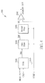
- FIG. 1 is a diagram illustrating a signal demodulation apparatus 100 according to an embodiment of the present invention.
- the signal demodulation apparatus 100 may be a demodulator used to demodulate a Near field communication (NFC) signal.
- the NFC signal may be an amplitude modulated signal having carrier frequency of 13.56MHz.
- the data rate of the NFC signal may vary from 106Kb/s to 6.78Mb/s, and the modulation indices may vary from 10% to 100%.
- the signal demodulation apparatus 100 comprises a clock generation device 102 and a demodulation device 104.
- the clock generation device 102 is arranged to receive an inputting modulation signal MOD_IN.
- the inputting modulation signal MOD_IN may be received by an antenna (not shown), and the antenna is arranged to receive a wireless NFC signal from a NFC device or NFC host.
- the clock generation device 102 is arranged to generate a clock signal CKS according to the inputting modulation signal MOD_IN.
- the demodulation device 104 is coupled to the clock generation device 102.
- the demodulation device 104 is arranged to receive the clock signal CKS and the inputting modulation signal MOD_IN, and to demodulate the inputting modulation signal MOD_IN to generate a demodulation signal DEMOD_OUT according to the clock signal CKS.
- a signal edge of the clock signal CKS substantially aligns to a turning point of the inputting modulation signal MOD_IN, in which the signal edge may be the rising edge or the falling edge of the clock signal CKS, and the turning point of the inputting modulation signal may be a peak (e.g. the maximum voltage) or a valley (e.g. the minimum voltage) of the inputting modulation signal MOD_IN.
- the signal edge of the clock signal CKS may precisely locate on the turning point of the inputting modulation signal MOD_IN or just close to the turning point of the inputting modulation signal MOD_IN.
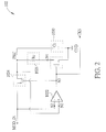
- FIG. 2 is a diagram illustrating a clock generation device 102 according to an embodiment of the present invention.
- the clock generation device 102 comprises a comparator 1022, a first transistor 1024, a second transistor 1026, a resistor 1028, and a capacitor 1030.
- the comparator 1022 has a first input terminal N1 (e.g. the negative input terminal) for receiving the inputting modulation signal MOD_IN.
- the first transistor 1024 has a first connecting terminal (e.g. a source terminal) for receiving the inputting modulation signal MOD_IN, a second connecting terminal (e.g. a drain terminal) coupled to a second input terminal N2 (e.g.
- the first transistor 1024 may be a P-type field-effect transistor.
- the second transistor 1026 has a controlling terminal coupled to the output terminal N3 of the comparator 1022, and a first connecting terminal (e.g. a source terminal) coupled to a reference voltage, i.e. the ground voltage GND.
- the resistor 1028 has a resistance of R c .
- the resistor 1028 has a first terminal coupled to a second connecting terminal (e.g. a drain terminal) N4 of the second transistor 1026, and a second terminal coupled to the second connecting terminal (i.e. N2) of the first transistor 1024.
- the second transistor 1026 may be an N-type field-effect transistor.
- the capacitor 1030 has a capacitance of C c .
- the capacitor 1030 has a first terminal coupled to the second connecting terminal (i.e. N2) of the first transistor 1024, and a second terminal coupled to the reference voltage, i.e. the ground voltage GND.
- the clock signal CKS is a signal on the output terminal N3 of the comparator 1022.
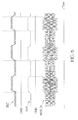
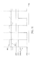
- FIG. 3 is a timing diagram illustrating the waveforms of the clock signal CKS, the inputting modulation signal MOD_IN, and a signal PKC on the second input terminal N2 of the comparator 1022 according to an embodiment of the present invention.
- the first comparator 1022 compares the voltages on the first input terminal N1 and the second input terminal N2. It is assumed that the voltage on the first input terminal N1 is lower than the voltage on the second input terminal N2 before time t1. Therefore, the voltage on the output terminal N3 of the comparator 1022 is a high voltage level VDD before time t1.
- the first transistor 1024 When the voltage on the output terminal N3 is the high voltage level VDD, the first transistor 1024 is turned off and the second transistor 1026 is turned on. This because the first transistor 1024 is P-type field-effect transistor and the second transistor 1026 is N-type field-effect transistor in this embodiment. Accordingly, the electric charges on the capacitor 1030 (i.e. the second input terminal N2) is discharged by the resistor 1028 such that the voltage (i.e. the signal PKC) on the second input terminal N2 decreases gradually before time t1.
- the comparator 1022 switches the voltage of the output terminal N3 to a low voltage level (e.g. GND) from the high voltage level VDD.
- a low voltage level e.g. GND
- the first transistor 1024 is turned on and the second transistor 1026 is turned off.
- the first transistor 1024 charges the capacitor 1030 after time t1 such that the voltage on the second input terminal N2 (i.e. the signal PKC) follows the voltage of the inputting modulation signal MOD_IN as shown in FIG. 3 .
- the voltage on the second input terminal N2 will follow the voltage of the inputting modulation signal MOD_IN, which means that the voltage on the first input terminal N1 is higher than the voltage on the second input terminal N2. Therefore, the voltage on the output terminal N3 is kept on the low voltage level GND after time t1.
- the voltage of the inputting modulation signal MOD_IN starts to decrease.
- the voltage of the inputting modulation signal MOS_IN crosses the voltage of the signal PKC such that the voltage on the first input terminal N1 is lower than the voltage on the second input terminal.
- the comparator 1022 switches the voltage on the output terminal N3 into the high voltage level VDD from the low voltage level GND, and the first transistor 1024 is turned off and the second transistor 1026 is turned on.
- the electric charges on the capacitor 1030 i.e. the second input terminal N2 is again discharged by the resistor 1028 such that the voltage (i.e. the signal PKC) on the second input terminal N2 decreases gradually until the inputting modulation signal MOD_IN crosses the signal PKC at time t3.
- the operation repeats.
- a narrow pulse i.e. the clock signal CKS
- the clock signal CKS having rising edges/falling edges aligned to the peaks of the inputting modulation signal MOD_IN is generated.
- a clock signal having rising edges/falling edges aligned to the valleys of the inputting modulation signal MOD_IN can also be generated after the appropriate modifications are made to the clock generation device 102.
- the modified clock generation device thus the detailed description is omitted here for brevity.
- one skilled in the art may change the first transistor 1024 to be an N-type field-effect transistor, and change the second transistor 1026 to be a P-type field-effect transistor.
- T c is the period of the carrier of the inputting modulation signal MOD_IN.
- R c C c is the time-constant of the RC circuit of the resistor 1028 and the capacitor 1030.
- FIG. 4 is a diagram illustrating the demodulation device 104 according to a first embodiment of the present invention.
- the demodulation device 104 comprises a sample and hold circuit (SAH) 1042, a first filter 1044, a second filter 1046, and a comparator 1048.
- the sample and hold circuit 1042 is arranged to sample the inputting modulation signal MOD_IN to generate an envelope signal Sen by using the clock signal CKS.
- the first filter 1044 is arranged to filter out a first signal component in the envelope signal Sen to generate a first filtered signal Shf.
- the second filter 1046 is arranged to filter out a second signal component in the envelope signal Sen or the first filtered signal Shf to generate a second filtered signal Slf.
- the comparator 1048 has a first input terminal + (i.e. the positive input terminal) for receiving the second filtered signal Slf, a second input terminal - (i.e. the negative input terminal) for receiving a reference voltage VREF, and an output terminal for outputting the demodulation signal DEMOD_OUT.
- the first filter 1044 and the second filter 1046 also receive the reference voltage VREF.
- the first filter 1044 is a high-pass filter arranged to change a DC (Direct current) signal of the envelope signal Sen into the reference voltage VREF, and to accordingly generate the first filtered signal Shf.
- the second filter 1046 is a low-pass filter arranged to filter out a sampling noise of the first filtered signal Shf, which can be regarded as the sampling noise of the envelope signal Sen, and to accordingly generate the second filtered signal Slf.
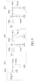
- FIG. 5 is a diagram illustrating the sample and hold circuit 1042, the first filter 1044, and the second filter 1046 according to an embodiment of the present invention.
- the sample and hold circuit 1042 comprises a switch 1042a and a capacitor 1042b.
- the switch 1042a has a first connecting terminal receiving the inputting modulation signal MOD_IN, a controlling terminal receiving the clock signal CKS for selectively coupling the inputting modulation signal MOD_IN to a second connecting terminal of the switch 1042.
- the capacitor 1042b has a first terminal coupled the second connecting terminal of the switch 1042a, and a second terminal coupled to a reference voltage, i.e. the ground voltage GND.
- the envelope signal Sen is a signal on the first terminal of the capacitor 1042b.
- the first filter 1044 comprises of a capacitor 1044a and a resistor 1044b.
- the capacitor 1044a has a first terminal receiving the envelope signal Sen.
- the resistor 1044b has a first terminal coupled to a second terminal of the capacitor 1044a, and a second terminal coupled to the reference voltage VREF.
- the first filtered signal Shf is a signal on the first terminal of the resistor 1044b.
- the second filter 1046 comprises a first resistor 1046a, a first capacitor 1046b, a second resistor 1046c, and a second capacitor 1046d.
- the first resistor 1046a has a first terminal receiving the first filtered signal Shf.
- the first capacitor 1046b has a first terminal coupled to a second terminal N5 of the first resistor 1046a, and a second terminal coupled to the reference voltage VREF.
- the second resistor 1046c has a first terminal coupled to the second terminal N5 of the first resistor 1046a.
- the second capacitor 1046d has a first terminal coupled to a second terminal of the second resistor 1046c, and a second terminal coupled to the reference voltage VREF.
- the second filtered signal Slf is a signal on the first terminal of the second capacitor 1046d.
- the sample and hold circuit 1042 uses the narrow pulses of the clock signal CKS to sample the voltage near the peak of the inputting modulation signal MOD_IN, and hold the voltage for the remaining of the carrier cycle time of the inputting modulation signal MOD_IN. Accordingly, when the amplitude of the carrier of the inputting modulation signal MOD_IN is high, the output of the sample and hold circuit 1042 is high, and when the amplitude of the carrier of the inputting modulation signal MOD_IN is low, the output of the sample and hold circuit 1042 is low. Therefore, the signal is already demodulated at the output of the sample and hold circuit 1042. However, the demodulated signal
- the high-pass filter i.e. 1044
- the low-pass filter i.e. 1046
- the cleaned-up and DC restored demodulated signal i.e. Slf
- is then fed to the non-inverting input i.e. the positive input terminal +
- the reference voltage VREF is fed to the inverting input (i.e. the negative input terminal -) of the comparator 1048.
- the signal at the output of the comparator 1048 is thus a rail-to-rail digital version of the demodulated signal.
- FIG. 6 is a timing diagram illustrating the inputting modulation signal MOD_IN, the envelope signal Sen, and the signal PKC according to an embodiment of the present invention.
- the inputting modulation signal MOD_IN is an amplitude modulated signal.
- the sample and hold circuit 1042 uses the clock signal CKS to sample the voltage of the peak or near the peak of the inputting modulation signal MOD_IN, and to hold on the voltage of the peak or near the peak of the inputting modulation signal MOD_IN to generate the envelope signal Sen. Therefore, the envelope signal Sen substantially equals to the envelope of the inputting modulation signal MOD_IN.
- the signal PKC is a triangle wave but has the similar envelope of the inputting modulation signal MOD_IN.
- FIG. 7 is a timing diagram illustrating the second filtered signal Slf, the reference voltage VREF, and the demodulation signal DEMOD_OUT according to an embodiment of the present invention.
- the reference voltage VREF is set in the middle voltage of the second filtered signal Slf because of DC restoration.
- the comparator 1048 outputs the high voltage level VDD, i.e. the supply voltage.
- the comparator 1048 outputs the low voltage level, i.e. the ground voltage GND.
- the comparator 1048 outputs a rail-to-rail square wave (i.e. the demodulation signal DEMOD_OUT) corresponding to the envelope of the inputting modulation signal MOD_IN.
- FIG. 8 is a diagram illustrating a demodulation device 804 according to a second embodiment of the present invention.
- the demodulation device 804 comprises a sample and hold circuit (SAH) 8042, a first filter 8044, a second filter 8046, and a comparator 8048.
- the sample and hold circuit 8042 is arranged to sample the inputting modulation signal MOD_IN' to generate an envelope signal Sen' by using the clock signal CKS'.
- the first filter 8044 is arranged to filter out a first signal component in the envelope signal Sen' to generate a first filtered signal Slf1'.
- the second filter 8046 is arranged to filter out a second signal component in the envelope signal Sen' to generate a second filtered signal Slf2'.
- the comparator 8048 has a first input terminal (i.e. the negative input terminal -) for receiving the first filtered signal Slf1', a second input terminal (i.e. the positive input terminal +) for receiving the second filtered signal Slf2', and an output terminal for outputting the demodulation signal DEMOD_OUT'.
- the first filter 8044 is a low-pass filter arranged to filter out an AC (Alternating current) signal of the envelope signal Sen', and to accordingly generate the first filtered signal Slf1'.
- the second filter 8046 is another low-pass filter arranged to filter out a sampling noise of the envelope signal Sen', and to accordingly generate the second filtered signal Slf2'. Therefore, the time constant of the first filter 8044 is larger than the time constant of the second filter 8046. More specifically, the first filter 8044 has a large time constant, and the second filter 8046 has a small time constant.
- FIG. 9 is a diagram illustrating the sample and hold circuit 8042, the first filter 8044, and the second filter 8046 according to an embodiment of the present invention.
- the sample and hold circuit 8042 comprises a switch 8042a and a capacitor 8042b.
- the switch 8042a has a first connecting terminal receiving the inputting modulation signal MOD_IN', a controlling terminal receiving the clock signal CKS' for selectively coupling the inputting modulation signal MOD_IN' to a second connecting terminal of the switch 8042a.
- the capacitor 8042b has a first terminal coupled the second connecting terminal of the switch 8042a, and a second terminal coupled to a reference voltage, i.e. the ground voltage GND.
- the envelope signal Sen' is a signal on the first terminal of the capacitor 8042b.
- the first filter 8044 comprises a first resistor 8044a, a first capacitor 8044b, a second resistor 8044c, and a second capacitor 8044d.
- the first resistor 8044a has a first terminal receiving the envelope signal Sen'.
- the first capacitor 8044b has a first terminal coupled to a second terminal N6 of the first resistor 8044a, and a second terminal coupled to a reference voltage, i.e. the ground voltage GND.
- the second resistor 8044c has a first terminal coupled to the second terminal N6 of the first resistor 8044a.
- the second capacitor 8044d has a first terminal coupled to a second terminal of the second resistor 8044c, and a second terminal coupled to the ground voltage GND.
- the first filtered signal Slf1' is a signal on the first terminal of the second capacitor 8044d.
- the second filter 8046 comprises a first resistor 8046a, a first capacitor 8046b, a second resistor 8046c, and a second capacitor 8046d.
- the first resistor 8046a has a first terminal receiving the envelope signal Sen".
- the first capacitor 8046b has a first terminal coupled to a second terminal N7 of the first resistor 8046a, and a second terminal coupled to the ground voltage GND.
- the second resistor 8046c has a first terminal coupled to the second terminal N7 of the first resistor 8046a.
- the second capacitor 8046d has a first terminal coupled to a second terminal of the second resistor 8046c, and a second terminal coupled to the ground voltage GND.
- the second filtered signal Slf2' is a signal on the first terminal of the second capacitor 8046d.
- the first capacitor 8044b, the second capacitor 8044d, the first capacitor 8046b, and the second capacitor 8046d may have the same capacitance. Accordingly, the resistances of the first resistor 8044a and the second resistor 8044c need to be much larger than the resistances of the first resistor 8046a and the second resistor 8046c. For example, the resistances of the first resistor 8044a and the second resistor 8044c are 40 times larger than the resistances of the first resistor 8046a and the second resistor 8046c whereas the first capacitor 8044b, the second capacitor 8044d, the first capacitor 8046b, and the second capacitor 8046d have the same capacitance.
- the sample and hold circuit 8042 is similar to the above sample and hold circuit 1042. Therefore, the signal is already demodulated at the output of the sample and hold circuit 8042.
- the demodulated signal i.e. the output of the sample and hold circuit 8042
- the large time-constant low-pass filter i.e. 8044
- the demodulated signal i.e. the output of the sample and hold circuit 8042
- the small time-constant low-pass filter i.e. 8046
- the output of the large time-constant low-pass filter is fed to the inverting input (i.e.
- the negative input terminal -) of the comparator 8048 while the output of the small time-constant low-pass filter is fed to the non-inverting input (i.e. the positive input terminal +) of the comparator 8048.
- the signal at the output of the comparator 8048 is thus a rail-to-rail digital version of the demodulated signal. It is noted that in this embodiment, no restoration of DC level of the demodulated signal is required.
- FIG. 10 is a timing diagram illustrating the first filtered signal Slf1', the second filtered signal Slf2', and the demodulation signal DEMOD_OUT' according to an embodiment of the present invention.
- the voltage of the first filtered signal Slf1' is in the middle of the second filtered signal Slf2'.
- the comparator 8048 outputs the high voltage level VDD, i.e. the supply voltage.
- the comparator 8048 outputs the low voltage level, i.e. the ground voltage GND.
- the comparator 8048 outputs a rail-to-rail square wave (i.e. the demodulation signal DEMOD_OUT') corresponding to the envelope of the inputting modulation signal MOD_IN'.
- the demodulation apparatus 100 is an analog demodulator without using an analog-to-digital converter. Therefore, the proposed demodulation apparatus 100 is a simple, low cost, and low power consumption demodulator.
- FIG. 11 is a flowchart illustrating a signal demodulation method 1100 according to an embodiment of the present invention. Provided that substantially the same result is achieved, the steps of the flowchart shown in FIG. 11 need not be in the exact order shown and need not be contiguous; that is, other steps can be intermediate.
- the signal demodulation method 1100 comprises the steps:
- the present demodulation apparatus and the related method applied an analog demodulation scheme to extract the envelope of an inputting NFC signal. Therefore, the proposed demodulation apparatus is a simple, low cost, and low power consumption demodulator.
Landscapes
- Engineering & Computer Science (AREA)
- Computer Networks & Wireless Communication (AREA)
- Signal Processing (AREA)
- Analogue/Digital Conversion (AREA)
- Digital Transmission Methods That Use Modulated Carrier Waves (AREA)
Abstract
Description
- The present invention relates to a signal demodulation apparatus, and more particularly to an analog NFC signal demodulator according to the characterizing clause of
claim 1. - Short-range, standards-based contactless connectivity technology such as Near field communication (NFC) uses magnetic field induction to enable communication between electronic devices in close proximity. Based on RFID technology, NFC provides a medium for the identification protocols that validates secure data transfer. The signal of the NFC is modulated by ASK (Amplitude shift keying) modulation. To receive the data of the NFC signal correctly, the envelope of the NFC signal should first be extracted. In other words, the rising edge and the falling edge of the envelope of the NFC signal should be precisely detected in order to correctly demodulate the data of the NFC signal. Conventionally, a digital demodulation scheme is always used to demodulate the NFC signal because the digital demodulation scheme can easily handle various modulation schemes of the NFC signal. However, the digital demodulation scheme is expensive in terms of die. This is because at least one high resolution analog-to-digital converter must be used to convert the receiving signal into the digital signal, and the analog-to-digital converter always occupies a large area of the die. Moreover, the large power consumption of the analog-to-digital converter can be another drawback of prior art. Therefore, providing a simplified, low cost, and low power demodulation scheme to detect the envelope of the NFC signal is an urgent problem in the NFC field.
- This in mind, the present invention aims at providing an analog NFC signal demodulator to solve the drawback of prior art.
- This is achieved by a signal demodulation apparatus according to
claim 1. The dependent claims pertain to corresponding further developments and improvements. - As will be seen more clearly from the detailed description following below, in an embodiment, the claimed signal demodulation apparatus is disclosed. The signal demodulation apparatus includes a clock generation device, and a demodulation device. The clock generation device is arranged to generate a clock signal according to an inputting modulation signal. The demodulation device is arranged to demodulate the inputting modulation signal to generate a demodulation signal according to the clock signal, wherein a signal edge of the clock signal substantially aligns to a turning point of the inputting modulation signal.
- In the following, the invention is further illustrated by way of example, taking reference to the accompanying drawings. Thereof
-
FIG. 1 is a diagram illustrating a signal demodulation apparatus according to an embodiment of the present invention. -
FIG. 2 is a diagram illustrating a clock generation device according to an embodiment of the present invention. -
Fig. 3 is a timing diagram illustrating the waveforms of a clock signal, an inputting modulation signal, and a signal on the second input terminal of a comparator according to an embodiment of the present invention. -
FIG. 4 is a diagram illustrating a demodulation device according to a first embodiment of the present invention. -
FIG. 5 is a diagram illustrating a sample and hold circuit, a first filter, and a second filter according to an embodiment of the present invention. -
FIG. 6 is a timing diagram illustrating an inputting modulation signal, an envelope signal, and a signal according to an embodiment of the present invention. -
FIG. 7 is a timing diagram illustrating a second filtered signal, a reference voltage, and a demodulation signal according to an embodiment of the present invention. -
FIG. 8 is a diagram illustrating a demodulation device according to a second embodiment of the present invention. -
FIG. 9 is a diagram illustrating a sample and hold circuit, a first filter, and a second filter according to an embodiment of the present invention. -
FIG. 10 is a timing diagram illustrating a first filtered signal, a second filtered signal, and a demodulation signal according to an embodiment of the present invention. -
FIG. 11 is a flowchart illustrating a signal demodulation method according to an embodiment of the present invention. - Please refer to
FIG. 1 , which is a diagram illustrating asignal demodulation apparatus 100 according to an embodiment of the present invention. Thesignal demodulation apparatus 100 may be a demodulator used to demodulate a Near field communication (NFC) signal. The NFC signal may be an amplitude modulated signal having carrier frequency of 13.56MHz. The data rate of the NFC signal may vary from 106Kb/s to 6.78Mb/s, and the modulation indices may vary from 10% to 100%. Thesignal demodulation apparatus 100 comprises aclock generation device 102 and ademodulation device 104. Theclock generation device 102 is arranged to receive an inputting modulation signal MOD_IN. The inputting modulation signal MOD_IN may be received by an antenna (not shown), and the antenna is arranged to receive a wireless NFC signal from a NFC device or NFC host. Theclock generation device 102 is arranged to generate a clock signal CKS according to the inputting modulation signal MOD_IN. Thedemodulation device 104 is coupled to theclock generation device 102. Thedemodulation device 104 is arranged to receive the clock signal CKS and the inputting modulation signal MOD_IN, and to demodulate the inputting modulation signal MOD_IN to generate a demodulation signal DEMOD_OUT according to the clock signal CKS. - According to the embodiment, a signal edge of the clock signal CKS substantially aligns to a turning point of the inputting modulation signal MOD_IN, in which the signal edge may be the rising edge or the falling edge of the clock signal CKS, and the turning point of the inputting modulation signal may be a peak (e.g. the maximum voltage) or a valley (e.g. the minimum voltage) of the inputting modulation signal MOD_IN. It should be noted that the signal edge of the clock signal CKS may precisely locate on the turning point of the inputting modulation signal MOD_IN or just close to the turning point of the inputting modulation signal MOD_IN.
- Please refer to
FIG. 2 , which is a diagram illustrating aclock generation device 102 according to an embodiment of the present invention. Theclock generation device 102 comprises acomparator 1022, afirst transistor 1024, a second transistor 1026, aresistor 1028, and acapacitor 1030. Thecomparator 1022 has a first input terminal N1 (e.g. the negative input terminal) for receiving the inputting modulation signal MOD_IN. Thefirst transistor 1024 has a first connecting terminal (e.g. a source terminal) for receiving the inputting modulation signal MOD_IN, a second connecting terminal (e.g. a drain terminal) coupled to a second input terminal N2 (e.g. the positive input terminal) of thecomparator 1022, and a controlling terminal coupled to an output terminal N3 of thecomparator 1022. Thefirst transistor 1024 may be a P-type field-effect transistor. The second transistor 1026 has a controlling terminal coupled to the output terminal N3 of thecomparator 1022, and a first connecting terminal (e.g. a source terminal) coupled to a reference voltage, i.e. the ground voltage GND. Theresistor 1028 has a resistance of Rc. Theresistor 1028 has a first terminal coupled to a second connecting terminal (e.g. a drain terminal) N4 of the second transistor 1026, and a second terminal coupled to the second connecting terminal (i.e. N2) of thefirst transistor 1024. The second transistor 1026 may be an N-type field-effect transistor. Thecapacitor 1030 has a capacitance of Cc. Thecapacitor 1030 has a first terminal coupled to the second connecting terminal (i.e. N2) of thefirst transistor 1024, and a second terminal coupled to the reference voltage, i.e. the ground voltage GND. According to the embodiment, the clock signal CKS is a signal on the output terminal N3 of thecomparator 1022. - To illustrate the operation of the
clock generation device 102,FIG. 3 is presented.Fig. 3 is a timing diagram illustrating the waveforms of the clock signal CKS, the inputting modulation signal MOD_IN, and a signal PKC on the second input terminal N2 of thecomparator 1022 according to an embodiment of the present invention. When the inputting modulation signal MOD_IN is transmitted to theclock generation device 102, thefirst comparator 1022 compares the voltages on the first input terminal N1 and the second input terminal N2. It is assumed that the voltage on the first input terminal N1 is lower than the voltage on the second input terminal N2 before time t1. Therefore, the voltage on the output terminal N3 of thecomparator 1022 is a high voltage level VDD before time t1. When the voltage on the output terminal N3 is the high voltage level VDD, thefirst transistor 1024 is turned off and the second transistor 1026 is turned on. This because thefirst transistor 1024 is P-type field-effect transistor and the second transistor 1026 is N-type field-effect transistor in this embodiment. Accordingly, the electric charges on the capacitor 1030 (i.e. the second input terminal N2) is discharged by theresistor 1028 such that the voltage (i.e. the signal PKC) on the second input terminal N2 decreases gradually before time t1. - Then, the voltage of the inputting modulation signal MOD_IN meets the voltage of the signal PKC at time t1, and after that, the
comparator 1022 switches the voltage of the output terminal N3 to a low voltage level (e.g. GND) from the high voltage level VDD. When the voltage on the output terminal N3 is the low voltage level GND, thefirst transistor 1024 is turned on and the second transistor 1026 is turned off. As a result, thefirst transistor 1024 charges thecapacitor 1030 after time t1 such that the voltage on the second input terminal N2 (i.e. the signal PKC) follows the voltage of the inputting modulation signal MOD_IN as shown inFIG. 3 . More specifically, if the voltage of the inputting modulation signal MOD_IN keeps increasing after time t1, then the voltage on the second input terminal N2 will follow the voltage of the inputting modulation signal MOD_IN, which means that the voltage on the first input terminal N1 is higher than the voltage on the second input terminal N2. Therefore, the voltage on the output terminal N3 is kept on the low voltage level GND after time t1. - However, after the voltage of the inputting modulation signal MOD_IN reaches the maximum voltage, the voltage of the inputting modulation signal MOD_IN starts to decrease. At time t2, the voltage of the inputting modulation signal MOS_IN crosses the voltage of the signal PKC such that the voltage on the first input terminal N1 is lower than the voltage on the second input terminal. Then, the
comparator 1022 switches the voltage on the output terminal N3 into the high voltage level VDD from the low voltage level GND, and thefirst transistor 1024 is turned off and the second transistor 1026 is turned on. - After time t2, the electric charges on the capacitor 1030 (i.e. the second input terminal N2) is again discharged by the
resistor 1028 such that the voltage (i.e. the signal PKC) on the second input terminal N2 decreases gradually until the inputting modulation signal MOD_IN crosses the signal PKC at time t3. At time t3, the operation repeats. - According to
FIG. 3 , it is seen that a narrow pulse (i.e. the clock signal CKS), which is aligned/synchronized to the peak of the inputting modulation signal MOS_IN, is generated at the output terminal N3. In other words, the clock signal CKS having rising edges/falling edges aligned to the peaks of the inputting modulation signal MOD_IN is generated. It should be noted that a clock signal having rising edges/falling edges aligned to the valleys of the inputting modulation signal MOD_IN can also be generated after the appropriate modifications are made to theclock generation device 102. Those skilled in the art are appreciated to understand the modified clock generation device, thus the detailed description is omitted here for brevity. For example, one skilled in the art may change thefirst transistor 1024 to be an N-type field-effect transistor, and change the second transistor 1026 to be a P-type field-effect transistor. - According to the embodiment, the pulse width Tp of the clock signal CKS can be expressed by the following equation (1):

- Tc is the period of the carrier of the inputting modulation signal MOD_IN. RcCc is the time-constant of the RC circuit of the
resistor 1028 and thecapacitor 1030. - Please refer to
FIG. 4 , which is a diagram illustrating thedemodulation device 104 according to a first embodiment of the present invention. Thedemodulation device 104 comprises a sample and hold circuit (SAH) 1042, afirst filter 1044, asecond filter 1046, and acomparator 1048. The sample and holdcircuit 1042 is arranged to sample the inputting modulation signal MOD_IN to generate an envelope signal Sen by using the clock signal CKS. Thefirst filter 1044 is arranged to filter out a first signal component in the envelope signal Sen to generate a first filtered signal Shf. Thesecond filter 1046 is arranged to filter out a second signal component in the envelope signal Sen or the first filtered signal Shf to generate a second filtered signal Slf. Thecomparator 1048 has a first input terminal + (i.e. the positive input terminal) for receiving the second filtered signal Slf, a second input terminal - (i.e. the negative input terminal) for receiving a reference voltage VREF, and an output terminal for outputting the demodulation signal DEMOD_OUT. Thefirst filter 1044 and thesecond filter 1046 also receive the reference voltage VREF. - According to the embodiment, the
first filter 1044 is a high-pass filter arranged to change a DC (Direct current) signal of the envelope signal Sen into the reference voltage VREF, and to accordingly generate the first filtered signal Shf. Thesecond filter 1046 is a low-pass filter arranged to filter out a sampling noise of the first filtered signal Shf, which can be regarded as the sampling noise of the envelope signal Sen, and to accordingly generate the second filtered signal Slf. - Please refer to
FIG. 5 , which is a diagram illustrating the sample and holdcircuit 1042, thefirst filter 1044, and thesecond filter 1046 according to an embodiment of the present invention. The sample and holdcircuit 1042 comprises aswitch 1042a and acapacitor 1042b. Theswitch 1042a has a first connecting terminal receiving the inputting modulation signal MOD_IN, a controlling terminal receiving the clock signal CKS for selectively coupling the inputting modulation signal MOD_IN to a second connecting terminal of theswitch 1042. Thecapacitor 1042b has a first terminal coupled the second connecting terminal of theswitch 1042a, and a second terminal coupled to a reference voltage, i.e. the ground voltage GND. According to the embodiment, the envelope signal Sen is a signal on the first terminal of thecapacitor 1042b. - The
first filter 1044 comprises of acapacitor 1044a and aresistor 1044b. Thecapacitor 1044a has a first terminal receiving the envelope signal Sen. Theresistor 1044b has a first terminal coupled to a second terminal of thecapacitor 1044a, and a second terminal coupled to the reference voltage VREF. According to the embodiment, the first filtered signal Shf is a signal on the first terminal of theresistor 1044b. - The
second filter 1046 comprises afirst resistor 1046a, afirst capacitor 1046b, asecond resistor 1046c, and asecond capacitor 1046d. Thefirst resistor 1046a has a first terminal receiving the first filtered signal Shf. Thefirst capacitor 1046b has a first terminal coupled to a second terminal N5 of thefirst resistor 1046a, and a second terminal coupled to the reference voltage VREF. Thesecond resistor 1046c has a first terminal coupled to the second terminal N5 of thefirst resistor 1046a. Thesecond capacitor 1046d has a first terminal coupled to a second terminal of thesecond resistor 1046c, and a second terminal coupled to the reference voltage VREF. According to the embodiment, the second filtered signal Slf is a signal on the first terminal of thesecond capacitor 1046d. - More specifically, when the
demodulation device 104 receives the inputting modulation signal MOD_IN and the clock signal CKS, the sample and holdcircuit 1042 uses the narrow pulses of the clock signal CKS to sample the voltage near the peak of the inputting modulation signal MOD_IN, and hold the voltage for the remaining of the carrier cycle time of the inputting modulation signal MOD_IN. Accordingly, when the amplitude of the carrier of the inputting modulation signal MOD_IN is high, the output of the sample and holdcircuit 1042 is high, and when the amplitude of the carrier of the inputting modulation signal MOD_IN is low, the output of the sample and holdcircuit 1042 is low. Therefore, the signal is already demodulated at the output of the sample and holdcircuit 1042. However, the demodulated signal - (i.e. the output of the sample and hold circuit 1042) has a high DC level and also contains some noise because of the sampling operation. Then, the high-pass filter (i.e. 1044) restores/changes the DC level of the demodulated signal to a predetermined reference level (i.e. VREF). The low-pass filter (i.e. 1046) removes the sampling noise from the demodulated signal. The cleaned-up and DC restored demodulated signal (i.e. Slf) is then fed to the non-inverting input (i.e. the positive input terminal +) of the
comparator 1048 while the reference voltage VREF is fed to the inverting input (i.e. the negative input terminal -) of thecomparator 1048. The signal at the output of thecomparator 1048 is thus a rail-to-rail digital version of the demodulated signal. - Please refer to
FIG. 6 , which is a timing diagram illustrating the inputting modulation signal MOD_IN, the envelope signal Sen, and the signal PKC according to an embodiment of the present invention. The inputting modulation signal MOD_IN is an amplitude modulated signal. The sample and holdcircuit 1042 uses the clock signal CKS to sample the voltage of the peak or near the peak of the inputting modulation signal MOD_IN, and to hold on the voltage of the peak or near the peak of the inputting modulation signal MOD_IN to generate the envelope signal Sen. Therefore, the envelope signal Sen substantially equals to the envelope of the inputting modulation signal MOD_IN. Moreover, the signal PKC is a triangle wave but has the similar envelope of the inputting modulation signal MOD_IN. - Please refer to
FIG. 7 , which is a timing diagram illustrating the second filtered signal Slf, the reference voltage VREF, and the demodulation signal DEMOD_OUT according to an embodiment of the present invention. The reference voltage VREF is set in the middle voltage of the second filtered signal Slf because of DC restoration. As a result, when the voltage of the second filtered signal Slf is higher than the reference voltage VREF, thecomparator 1048 outputs the high voltage level VDD, i.e. the supply voltage. When the voltage of the second filtered signal Slf is lower than the reference voltage VREF, thecomparator 1048 outputs the low voltage level, i.e. the ground voltage GND. As a result, thecomparator 1048 outputs a rail-to-rail square wave (i.e. the demodulation signal DEMOD_OUT) corresponding to the envelope of the inputting modulation signal MOD_IN. - Please refer to
FIG. 8 , which is a diagram illustrating ademodulation device 804 according to a second embodiment of the present invention. Thedemodulation device 804 comprises a sample and hold circuit (SAH) 8042, afirst filter 8044, asecond filter 8046, and acomparator 8048. The sample and holdcircuit 8042 is arranged to sample the inputting modulation signal MOD_IN' to generate an envelope signal Sen' by using the clock signal CKS'. Thefirst filter 8044 is arranged to filter out a first signal component in the envelope signal Sen' to generate a first filtered signal Slf1'. Thesecond filter 8046 is arranged to filter out a second signal component in the envelope signal Sen' to generate a second filtered signal Slf2'. Thecomparator 8048 has a first input terminal (i.e. the negative input terminal -) for receiving the first filtered signal Slf1', a second input terminal (i.e. the positive input terminal +) for receiving the second filtered signal Slf2', and an output terminal for outputting the demodulation signal DEMOD_OUT'. - According to the embodiment, the
first filter 8044 is a low-pass filter arranged to filter out an AC (Alternating current) signal of the envelope signal Sen', and to accordingly generate the first filtered signal Slf1'. Thesecond filter 8046 is another low-pass filter arranged to filter out a sampling noise of the envelope signal Sen', and to accordingly generate the second filtered signal Slf2'. Therefore, the time constant of thefirst filter 8044 is larger than the time constant of thesecond filter 8046. More specifically, thefirst filter 8044 has a large time constant, and thesecond filter 8046 has a small time constant. - Please refer to
FIG. 9 , which is a diagram illustrating the sample and holdcircuit 8042, thefirst filter 8044, and thesecond filter 8046 according to an embodiment of the present invention. The sample and holdcircuit 8042 comprises aswitch 8042a and acapacitor 8042b. Theswitch 8042a has a first connecting terminal receiving the inputting modulation signal MOD_IN', a controlling terminal receiving the clock signal CKS' for selectively coupling the inputting modulation signal MOD_IN' to a second connecting terminal of theswitch 8042a. Thecapacitor 8042b has a first terminal coupled the second connecting terminal of theswitch 8042a, and a second terminal coupled to a reference voltage, i.e. the ground voltage GND. According to the embodiment, the envelope signal Sen' is a signal on the first terminal of thecapacitor 8042b. - The
first filter 8044 comprises afirst resistor 8044a, afirst capacitor 8044b, asecond resistor 8044c, and a second capacitor 8044d. Thefirst resistor 8044a has a first terminal receiving the envelope signal Sen'. Thefirst capacitor 8044b has a first terminal coupled to a second terminal N6 of thefirst resistor 8044a, and a second terminal coupled to a reference voltage, i.e. the ground voltage GND. Thesecond resistor 8044c has a first terminal coupled to the second terminal N6 of thefirst resistor 8044a. The second capacitor 8044d has a first terminal coupled to a second terminal of thesecond resistor 8044c, and a second terminal coupled to the ground voltage GND. According to the embodiment, the first filtered signal Slf1' is a signal on the first terminal of the second capacitor 8044d. - The
second filter 8046 comprises afirst resistor 8046a, afirst capacitor 8046b, asecond resistor 8046c, and a second capacitor 8046d. Thefirst resistor 8046a has a first terminal receiving the envelope signal Sen". Thefirst capacitor 8046b has a first terminal coupled to a second terminal N7 of thefirst resistor 8046a, and a second terminal coupled to the ground voltage GND. Thesecond resistor 8046c has a first terminal coupled to the second terminal N7 of thefirst resistor 8046a. The second capacitor 8046d has a first terminal coupled to a second terminal of thesecond resistor 8046c, and a second terminal coupled to the ground voltage GND. According to the embodiment, the second filtered signal Slf2' is a signal on the first terminal of the second capacitor 8046d. - According to the embodiment, the
first capacitor 8044b, the second capacitor 8044d, thefirst capacitor 8046b, and the second capacitor 8046d may have the same capacitance. Accordingly, the resistances of thefirst resistor 8044a and thesecond resistor 8044c need to be much larger than the resistances of thefirst resistor 8046a and thesecond resistor 8046c. For example, the resistances of thefirst resistor 8044a and thesecond resistor 8044c are 40 times larger than the resistances of thefirst resistor 8046a and thesecond resistor 8046c whereas thefirst capacitor 8044b, the second capacitor 8044d, thefirst capacitor 8046b, and the second capacitor 8046d have the same capacitance. - More specifically, the sample and hold
circuit 8042 is similar to the above sample and holdcircuit 1042. Therefore, the signal is already demodulated at the output of the sample and holdcircuit 8042. In this embodiment, the demodulated signal (i.e. the output of the sample and hold circuit 8042) is fed to the large time-constant low-pass filter (i.e. 8044) for generating the average level of the demodulated signal. The demodulated signal (i.e. the output of the sample and hold circuit 8042) is also fed to the small time-constant low-pass filter (i.e. 8046) to remove the sampling noise from the demodulated signal. The output of the large time-constant low-pass filter is fed to the inverting input (i.e. the negative input terminal -) of thecomparator 8048 while the output of the small time-constant low-pass filter is fed to the non-inverting input (i.e. the positive input terminal +) of thecomparator 8048. The signal at the output of thecomparator 8048 is thus a rail-to-rail digital version of the demodulated signal. It is noted that in this embodiment, no restoration of DC level of the demodulated signal is required. - Please refer to
FIG. 10 , which is a timing diagram illustrating the first filtered signal Slf1', the second filtered signal Slf2', and the demodulation signal DEMOD_OUT' according to an embodiment of the present invention. The voltage of the first filtered signal Slf1' is in the middle of the second filtered signal Slf2'. As a result, when the voltage of the second filtered signal Slf2' is higher than the first filtered signal Slf1', thecomparator 8048 outputs the high voltage level VDD, i.e. the supply voltage. When the voltage of the second filtered signal Slf2' is lower than the first filtered signal Slf1', thecomparator 8048 outputs the low voltage level, i.e. the ground voltage GND. As a result, thecomparator 8048 outputs a rail-to-rail square wave (i.e. the demodulation signal DEMOD_OUT') corresponding to the envelope of the inputting modulation signal MOD_IN'. - According to the above description, the
demodulation apparatus 100 is an analog demodulator without using an analog-to-digital converter. Therefore, the proposeddemodulation apparatus 100 is a simple, low cost, and low power consumption demodulator. - In summary, the operation of the
demodulation apparatus 100 can be summarized into the processes ofFIG. 11. FIG. 11 is a flowchart illustrating asignal demodulation method 1100 according to an embodiment of the present invention. Provided that substantially the same result is achieved, the steps of the flowchart shown inFIG. 11 need not be in the exact order shown and need not be contiguous; that is, other steps can be intermediate. Thesignal demodulation method 1100 comprises the steps: - Step 1102: Provide the
comparator 1022 having a first input terminal for receiving the inputting modulation signal MOD_IN; - Step 1104: Provide the
first transistor 1024 having a first connecting terminal for receiving the inputting modulation signal MOD_IN, a second connecting terminal coupled to a second input terminal of thecomparator 1022, and a controlling terminal coupled to an output terminal N3 of thecomparator 1022; - Step 1106: Provide the second transistor 1026 having a controlling terminal coupled to the output terminal N3 of the
comparator 1022, and a first connecting terminal coupled to the ground voltage GND; - Step 1108: Provide the
resistor 1028 having a first terminal coupled to a second connecting terminal of the second transistor 1026, and a second terminal coupled to the second connecting terminal of thefirst transistor 1024; - Step 1110: Provide the
capacitor 1030 having a first terminal coupled to the second connecting terminal of thefirst transistor 1024, and a second terminal coupled to the ground voltage GND, wherein the clock signal CKS is a signal on the output terminal N3 of thecomparator 1022; and - Step 1112: Demodulate the inputting modulation signal MOD_IN to generate the demodulation signal DEMOD_OUT according to the clock signal CKS, wherein a signal edge of the clock signal CKS substantially aligns to a turning point of the inputting modulation signal MOD_IN.
- Briefly, the present demodulation apparatus and the related method applied an analog demodulation scheme to extract the envelope of an inputting NFC signal. Therefore, the proposed demodulation apparatus is a simple, low cost, and low power consumption demodulator.
Claims (16)
- A signal demodulation apparatus (100), characterized by:a clock generation device (102), arranged to generate a clock signal according to an inputting modulation signal; anda demodulation device (104), arranged to demodulate the inputting modulation signal to generate a demodulation signal according to the clock signal;wherein a signal edge of the clock signal substantially aligns to a turning point of the inputting modulation signal.
- The signal demodulation apparatus (100) of claim 1, characterized in that the turning point of the inputting modulation signal is a peak or a valley of the inputting modulation signal.
- The signal demodulation apparatus (100) of claim 1, characterized in that the clock generation device (102) comprises:a comparator (1022), having a first input terminal for receiving the inputting modulation signal;a first transistor (1024), having a first connecting terminal for receiving the inputting modulation signal, a second connecting terminal coupled to a second input terminal of the comparator (1022), and a controlling terminal coupled to an output terminal of the comparator (1022);a second transistor (1026), having a controlling terminal coupled to the output terminal of the comparator (1022), and a first connecting terminal coupled to a reference voltage;a resistor (1028), having a first terminal coupled to a second connecting terminal of the second transistor (1026), and a second terminal coupled to the second connecting terminal of the first transistor (1024); anda capacitor (1030), having a first terminal coupled to the second connecting terminal of the first transistor (1024), and a second terminal coupled to the reference voltage;wherein the clock signal is a signal on the output terminal of the comparator (1022).
- The signal demodulation apparatus (100) of claim 1, characterized in that the demodulation device (104) comprises:a sample and hold circuit (1042), arranged to sample the inputting modulation signal to generate an envelope signal by using the clock signal;a first filter (1044), arranged to filter out a first signal component in the envelope signal to generate a first filtered signal;a second filter (1046), arranged to filter out a second signal component in the envelope signal to generate a second filtered signal; anda comparator (1048), having a first input terminal for receiving the second filtered signal, a second input terminal for receiving a first reference voltage, and an output terminal for outputting the demodulation signal.
- The signal demodulation apparatus (100) of claim 4, characterized in that the first filter (1044) is a high-pass filter arranged to change a DC (Direct current) signal of the envelope signal into the first reference voltage, and to accordingly generate the first filtered signal.
- The signal demodulation apparatus (100) of claim 4, characterized in that the second filter (1046) is a low-pass filter arranged to filter out a sampling noise of the envelope signal, and to accordingly generate the second filtered signal.
- The signal demodulation apparatus (100) of claim 4, characterized in that the sample and hold circuit (1042) comprises:a switch (1042a), having a first connecting terminal receiving the inputting modulation signal, a controlling terminal receiving the clock signal for selectively coupling the inputting modulation signal to a second connecting terminal of the switch; anda capacitor (1042b), having a first terminal coupled the second connecting terminal of the switch (1042a), and a second terminal coupled to a second reference voltage;wherein the envelope signal is a signal on the first terminal of the capacitor (1042b).
- The signal demodulation apparatus (100) of claim 4, characterized in that the first filter (1044) comprises:a capacitor (1044a), having a first terminal receiving the envelope signal; anda resistor (1044b), having a first terminal coupled to a second terminal of the capacitor (1044a), and a second terminal coupled to the first reference voltage;wherein the first filtered signal is a signal on the first terminal of the resistor (1044a).
- The signal demodulation apparatus (100) of claim 4, characterized in that the second filter (1046) comprises:a first resistor (1046a), having a first terminal receiving the first filtered signal;a first capacitor (1046b), having a first terminal coupled to a second terminal of the first resistor (1046a), and a second terminal coupled to the first reference voltage;a second resistor (1046c), having a first terminal coupled to the second terminal of the first resistor (1046a); anda second capacitor (1046d), having a first terminal coupled to a second terminal of the second resistor (1046c), and a second terminal coupled to the first reference voltage;wherein the second filtered signal is a signal on the first terminal of the second capacitor (1046d).
- The signal demodulation apparatus (100) of claim 1, characterized in that the demodulation device (804) comprises:a sample and hold circuit (8042), arranged to sample the inputting modulation signal to generate an envelope signal by using the clock signal;a first filter (8044), arranged to filter out a first signal component in the envelope signal to generate a first filtered signal;a second filter (8046), arranged to filter out a second signal component in the envelope signal to generate a second filtered signal; anda comparator (8048), having a first input terminal for receiving the first filtered signal, a second input terminal for receiving the second filtered signal, and an output terminal for outputting the demodulation signal.
- The signal demodulation apparatus (100) of claim 10, characterized in that a time constant of the first filter (8044) is substantially larger than the time constant of the second filter (8046).
- The signal demodulation apparatus (100) of claim 10, characterized in that the first filter (8044) is a low-pass filter arranged to filter out an AC (Alternating current) signal of the envelope signal, and to accordingly generate the first filtered signal.
- The signal demodulation apparatus (100) of claim 10, characterized in that the second filter (8046) is a low-pass filter arranged to filter out a sampling noise of the envelope signal, and to accordingly generate the second filtered signal.
- The signal demodulation apparatus (100) of claim 10, characterized in that the sample and hold circuit (8042) comprises:a switch (8042a), having a first connecting terminal receiving the inputting modulation signal, a controlling terminal receiving the clock signal for selectively coupling the inputting modulation signal to a second connecting terminal of the switch (8042a); anda capacitor (8042b), having a first terminal coupled the second connecting terminal of the switch (8042a), and a second terminal coupled to a reference voltage;wherein the envelope signal is a signal on the first terminal of the capacitor (8042b).
- The signal demodulation apparatus (100) of claim 10, characterized in that the first filter (8044) comprises:a first resistor (8044a), having a first terminal receiving the envelope signal;a first capacitor (8044b), having a first terminal coupled to a second terminal of the first resistor (8044a), and a second terminal coupled to a reference voltage;a second resistor (8044c), having a first terminal coupled to the second terminal of the first resistor (8044a); anda second capacitor (8044d), having a first terminal coupled to a second terminal of the second resistor (8044c), and a second terminal coupled to the reference voltage;wherein the first filtered signal is a signal on the first terminal of the second capacitor (8044d).
- The signal demodulation apparatus (100) of claim 10, characterized in that the second filter (8046) comprises:a first resistor (8046a), having a first terminal receiving the envelope signal;a first capacitor (8046b), having a first terminal coupled to a second terminal of the first resistor (8046a), and a second terminal coupled to a reference voltage;a second resistor (8046c), having a first terminal coupled to the second terminal of the first resistor (8046a); anda second capacitor (8046d), having a first terminal coupled to a second terminal of the second resistor (8046c), and a second terminal coupled to the reference voltage;wherein the second filtered signal is a signal on the first terminal of the second capacitor (8046d).
Applications Claiming Priority (2)
| Application Number | Priority Date | Filing Date | Title |
|---|---|---|---|
| US201462082556P | 2014-11-20 | 2014-11-20 | |
| US14/803,131 US9461852B2 (en) | 2014-11-20 | 2015-07-20 | Signal demodulation apparatus and signal demodulation method |
Publications (2)
| Publication Number | Publication Date |
|---|---|
| EP3024187A1 true EP3024187A1 (en) | 2016-05-25 |
| EP3024187B1 EP3024187B1 (en) | 2019-11-13 |
Family
ID=53785508
Family Applications (1)
| Application Number | Title | Priority Date | Filing Date |
|---|---|---|---|
| EP15179253.8A Active EP3024187B1 (en) | 2014-11-20 | 2015-07-31 | Signal demodulation apparatus |
Country Status (3)
| Country | Link |
|---|---|
| US (1) | US9461852B2 (en) |
| EP (1) | EP3024187B1 (en) |
| CN (1) | CN105635011B (en) |
Cited By (1)
| Publication number | Priority date | Publication date | Assignee | Title |
|---|---|---|---|---|
| EP3579438A1 (en) * | 2018-06-05 | 2019-12-11 | EM Microelectronic-Marin SA | Demodulator for an rfid circuit |
Families Citing this family (4)
| Publication number | Priority date | Publication date | Assignee | Title |
|---|---|---|---|---|
| WO2017094045A1 (en) * | 2015-12-04 | 2017-06-08 | 日本電気株式会社 | Reception circuit, reception device, and reception method |
| EP3584948A1 (en) * | 2018-06-19 | 2019-12-25 | STMicroelectronics razvoj polprevodnikov d.o.o. | Protocol detection and decoding in multiprotocol tag, and corresponding integrated circuit |
| CN109474308B (en) * | 2018-12-19 | 2021-07-09 | 深圳易联凯科技有限公司 | Signal demodulation system and method |
| CN121279329B (en) * | 2025-12-09 | 2026-02-27 | 北京兆讯恒达技术有限公司 | A demodulation method, apparatus, electronic device, and medium for an analog card. |
Citations (2)
| Publication number | Priority date | Publication date | Assignee | Title |
|---|---|---|---|---|
| US20100039227A1 (en) * | 2008-08-13 | 2010-02-18 | Electronics And Telecommunications Research Institute | Apparatus and method for demodulating subcarrier tag signal in rfid reader |
| EP2280488A1 (en) * | 2009-06-30 | 2011-02-02 | STMicroelectronics S.r.l. | Transmission and reception apparatus for digital signals |
Family Cites Families (6)
| Publication number | Priority date | Publication date | Assignee | Title |
|---|---|---|---|---|
| US5214409A (en) * | 1991-12-03 | 1993-05-25 | Avid Corporation | Multi-memory electronic identification tag |
| JP4579831B2 (en) * | 2003-07-25 | 2010-11-10 | パナソニック株式会社 | Modulation device, demodulation device, modulation method and demodulation method |
| CN100499617C (en) * | 2006-01-20 | 2009-06-10 | 清华大学 | Comparison and decision circuit in amplitude keying signal demodulation circuit module |
| US8135084B2 (en) * | 2006-07-31 | 2012-03-13 | Panasonic Corporation | Multiantenna receiving device |
| JP2009290783A (en) * | 2008-05-30 | 2009-12-10 | Canon Inc | Communication system, and method and program for controlling communication system, and storage medium |
| TWI401923B (en) * | 2009-06-06 | 2013-07-11 | Generalplus Technology Inc | Methods and apparatuses for adaptive clock reconstruction and decoding in audio frequency |
-
2015
- 2015-07-20 US US14/803,131 patent/US9461852B2/en not_active Expired - Fee Related
- 2015-07-31 EP EP15179253.8A patent/EP3024187B1/en active Active
- 2015-11-11 CN CN201510766248.3A patent/CN105635011B/en not_active Expired - Fee Related
Patent Citations (2)
| Publication number | Priority date | Publication date | Assignee | Title |
|---|---|---|---|---|
| US20100039227A1 (en) * | 2008-08-13 | 2010-02-18 | Electronics And Telecommunications Research Institute | Apparatus and method for demodulating subcarrier tag signal in rfid reader |
| EP2280488A1 (en) * | 2009-06-30 | 2011-02-02 | STMicroelectronics S.r.l. | Transmission and reception apparatus for digital signals |
Non-Patent Citations (3)
| Title |
|---|
| BASAVARAJ P. M. ET AL: "Design of Low Power ASK CMOS Demodulator Circuits for passive Ultra High Frequency Tag", INTERNATIONAL JOURNAL OF FUTURE COMPUTER AND COMMUNICATION, 1 January 2012 (2012-01-01), pages 369 - 371, XP055259274, ISSN: 2010-3751, DOI: 10.7763/IJFCC.2012.V1.98 * |
| FEI YUAN: "Design techniques for ASK demodulators of passive wireless microsystems: a state-of-the-art review", ANALOG INTEGRATED CIRCUITS AND SIGNAL PROCESSING, KLUWER ACADEMIC PUBLISHERS, BO, vol. 63, no. 1, 16 September 2009 (2009-09-16), pages 33 - 45, XP019786416, ISSN: 1573-1979 * |
| MARIO MENDIZABAL: "Low Power Demodulator Design for RFID Applications", 31 December 2012 (2012-12-31), XP055258725, Retrieved from the Internet <URL:http://scholar.uwindsor.ca/cgi/viewcontent.cgi?article=1131&context=etd> [retrieved on 20160316] * |
Cited By (3)
| Publication number | Priority date | Publication date | Assignee | Title |
|---|---|---|---|---|
| EP3579438A1 (en) * | 2018-06-05 | 2019-12-11 | EM Microelectronic-Marin SA | Demodulator for an rfid circuit |
| JP2019213199A (en) * | 2018-06-05 | 2019-12-12 | イーエム・ミクロエレクトロニク−マリン・エス アー | Demodulator for RFID circuit |
| US11012271B2 (en) | 2018-06-05 | 2021-05-18 | Em Microelectronic-Marin Sa | Demodulator for an RFID circuit |
Also Published As
| Publication number | Publication date |
|---|---|
| CN105635011B (en) | 2018-12-28 |
| US20160149736A1 (en) | 2016-05-26 |
| EP3024187B1 (en) | 2019-11-13 |
| CN105635011A (en) | 2016-06-01 |
| US9461852B2 (en) | 2016-10-04 |
Similar Documents
| Publication | Publication Date | Title |
|---|---|---|
| EP3024187B1 (en) | Signal demodulation apparatus | |
| US9791888B2 (en) | Power reception device and power transmission system | |
| CN105850021B (en) | Ammeters for Load Modulated Communication Receiver Architectures | |
| EP2752792B1 (en) | Receiver and method for near field communication | |
| EP1842284B1 (en) | A demodulator | |
| US20150207616A1 (en) | Adaptive envelope extracting apparatus, signal decoding apparatus and short-distance contactless communication apparatus applying the adaptive envelope extracting apparatus, and method thereof | |
| US9893771B2 (en) | Wireless charger using frequency aliasing FSK demodulation | |
| CN102594310B (en) | For the detector circuit of detection signal amplitude, transponder and method | |
| JP2004363684A (en) | Two-wire data communication method, system, control device, and data storage device | |
| US8076970B2 (en) | Adaptive demodulator | |
| KR101183729B1 (en) | Low Power Amplitude Shift Keying Demodulator with Self-Sampling Scheme | |
| CN100499617C (en) | Comparison and decision circuit in amplitude keying signal demodulation circuit module | |
| CN118784006A (en) | Receiving circuit and smart card including the same | |
| JP4573871B2 (en) | Demodulation circuit and electronic equipment | |
| CN112434774B (en) | Demodulation circuit of electronic tag and electronic tag | |
| JP3991006B2 (en) | ASK signal receiver | |
| Hou et al. | A 1-Mbps Frequency-Shift Keying Receiver for Inductively Powered Biomedical Applications | |
| Nabovati et al. | Ultra-low power BPSK demodulator for bio-implantable chips | |
| JP6590162B2 (en) | Electric field communication transceiver | |
| JP6492848B2 (en) | Demodulation circuit and wireless tag device using the same | |
| CN104299024B (en) | The demodulator circuit of contactless IC card | |
| KR100751064B1 (en) | Low Power RFID Demodulator for Data Recovery | |
| CN209514641U (en) | A radio frequency decoding circuit and decoding equipment | |
| EP3276844B1 (en) | Load-modulation detection component | |
| JP7297453B2 (en) | data slicer and receiver |
Legal Events
| Date | Code | Title | Description |
|---|---|---|---|
| AK | Designated contracting states |
Kind code of ref document: A1 Designated state(s): AL AT BE BG CH CY CZ DE DK EE ES FI FR GB GR HR HU IE IS IT LI LT LU LV MC MK MT NL NO PL PT RO RS SE SI SK SM TR |
|
| AX | Request for extension of the european patent |
Extension state: BA ME |
|
| PUAI | Public reference made under article 153(3) epc to a published international application that has entered the european phase |
Free format text: ORIGINAL CODE: 0009012 |
|
| 17P | Request for examination filed |
Effective date: 20160622 |
|
| RBV | Designated contracting states (corrected) |
Designated state(s): AL AT BE BG CH CY CZ DE DK EE ES FI FR GB GR HR HU IE IS IT LI LT LU LV MC MK MT NL NO PL PT RO RS SE SI SK SM TR |
|
| STAA | Information on the status of an ep patent application or granted ep patent |
Free format text: STATUS: EXAMINATION IS IN PROGRESS |
|
| 17Q | First examination report despatched |
Effective date: 20171019 |
|
| GRAP | Despatch of communication of intention to grant a patent |
Free format text: ORIGINAL CODE: EPIDOSNIGR1 |
|
| STAA | Information on the status of an ep patent application or granted ep patent |
Free format text: STATUS: GRANT OF PATENT IS INTENDED |
|
| INTG | Intention to grant announced |
Effective date: 20190717 |
|
| GRAS | Grant fee paid |
Free format text: ORIGINAL CODE: EPIDOSNIGR3 |
|
| GRAJ | Information related to disapproval of communication of intention to grant by the applicant or resumption of examination proceedings by the epo deleted |
Free format text: ORIGINAL CODE: EPIDOSDIGR1 |
|
| GRAL | Information related to payment of fee for publishing/printing deleted |
Free format text: ORIGINAL CODE: EPIDOSDIGR3 |
|
| STAA | Information on the status of an ep patent application or granted ep patent |
Free format text: STATUS: EXAMINATION IS IN PROGRESS |
|
| GRAR | Information related to intention to grant a patent recorded |
Free format text: ORIGINAL CODE: EPIDOSNIGR71 |
|
| STAA | Information on the status of an ep patent application or granted ep patent |
Free format text: STATUS: GRANT OF PATENT IS INTENDED |
|
| GRAA | (expected) grant |
Free format text: ORIGINAL CODE: 0009210 |
|
| STAA | Information on the status of an ep patent application or granted ep patent |
Free format text: STATUS: THE PATENT HAS BEEN GRANTED |
|
| INTG | Intention to grant announced |
Effective date: 20191003 |
|
| AK | Designated contracting states |
Kind code of ref document: B1 Designated state(s): AL AT BE BG CH CY CZ DE DK EE ES FI FR GB GR HR HU IE IS IT LI LT LU LV MC MK MT NL NO PL PT RO RS SE SI SK SM TR |
|
| REG | Reference to a national code |
Ref country code: CH Ref legal event code: EP Ref country code: AT Ref legal event code: REF Ref document number: 1202854 Country of ref document: AT Kind code of ref document: T Effective date: 20191115 |
|
| REG | Reference to a national code |
Ref country code: DE Ref legal event code: R096 Ref document number: 602015041515 Country of ref document: DE |
|
| REG | Reference to a national code |
Ref country code: IE Ref legal event code: FG4D |
|
| REG | Reference to a national code |
Ref country code: NL Ref legal event code: MP Effective date: 20191113 |
|
| REG | Reference to a national code |
Ref country code: LT Ref legal event code: MG4D |
|
| PG25 | Lapsed in a contracting state [announced via postgrant information from national office to epo] |
Ref country code: PT Free format text: LAPSE BECAUSE OF FAILURE TO SUBMIT A TRANSLATION OF THE DESCRIPTION OR TO PAY THE FEE WITHIN THE PRESCRIBED TIME-LIMIT Effective date: 20200313 Ref country code: NL Free format text: LAPSE BECAUSE OF FAILURE TO SUBMIT A TRANSLATION OF THE DESCRIPTION OR TO PAY THE FEE WITHIN THE PRESCRIBED TIME-LIMIT Effective date: 20191113 Ref country code: NO Free format text: LAPSE BECAUSE OF FAILURE TO SUBMIT A TRANSLATION OF THE DESCRIPTION OR TO PAY THE FEE WITHIN THE PRESCRIBED TIME-LIMIT Effective date: 20200213 Ref country code: PL Free format text: LAPSE BECAUSE OF FAILURE TO SUBMIT A TRANSLATION OF THE DESCRIPTION OR TO PAY THE FEE WITHIN THE PRESCRIBED TIME-LIMIT Effective date: 20191113 Ref country code: GR Free format text: LAPSE BECAUSE OF FAILURE TO SUBMIT A TRANSLATION OF THE DESCRIPTION OR TO PAY THE FEE WITHIN THE PRESCRIBED TIME-LIMIT Effective date: 20200214 Ref country code: BG Free format text: LAPSE BECAUSE OF FAILURE TO SUBMIT A TRANSLATION OF THE DESCRIPTION OR TO PAY THE FEE WITHIN THE PRESCRIBED TIME-LIMIT Effective date: 20200213 Ref country code: FI Free format text: LAPSE BECAUSE OF FAILURE TO SUBMIT A TRANSLATION OF THE DESCRIPTION OR TO PAY THE FEE WITHIN THE PRESCRIBED TIME-LIMIT Effective date: 20191113 Ref country code: LT Free format text: LAPSE BECAUSE OF FAILURE TO SUBMIT A TRANSLATION OF THE DESCRIPTION OR TO PAY THE FEE WITHIN THE PRESCRIBED TIME-LIMIT Effective date: 20191113 Ref country code: LV Free format text: LAPSE BECAUSE OF FAILURE TO SUBMIT A TRANSLATION OF THE DESCRIPTION OR TO PAY THE FEE WITHIN THE PRESCRIBED TIME-LIMIT Effective date: 20191113 Ref country code: SE Free format text: LAPSE BECAUSE OF FAILURE TO SUBMIT A TRANSLATION OF THE DESCRIPTION OR TO PAY THE FEE WITHIN THE PRESCRIBED TIME-LIMIT Effective date: 20191113 |
|
| PG25 | Lapsed in a contracting state [announced via postgrant information from national office to epo] |
Ref country code: HR Free format text: LAPSE BECAUSE OF FAILURE TO SUBMIT A TRANSLATION OF THE DESCRIPTION OR TO PAY THE FEE WITHIN THE PRESCRIBED TIME-LIMIT Effective date: 20191113 Ref country code: RS Free format text: LAPSE BECAUSE OF FAILURE TO SUBMIT A TRANSLATION OF THE DESCRIPTION OR TO PAY THE FEE WITHIN THE PRESCRIBED TIME-LIMIT Effective date: 20191113 Ref country code: IS Free format text: LAPSE BECAUSE OF FAILURE TO SUBMIT A TRANSLATION OF THE DESCRIPTION OR TO PAY THE FEE WITHIN THE PRESCRIBED TIME-LIMIT Effective date: 20200313 |
|
| PG25 | Lapsed in a contracting state [announced via postgrant information from national office to epo] |
Ref country code: AL Free format text: LAPSE BECAUSE OF FAILURE TO SUBMIT A TRANSLATION OF THE DESCRIPTION OR TO PAY THE FEE WITHIN THE PRESCRIBED TIME-LIMIT Effective date: 20191113 |
|
| PG25 | Lapsed in a contracting state [announced via postgrant information from national office to epo] |
Ref country code: RO Free format text: LAPSE BECAUSE OF FAILURE TO SUBMIT A TRANSLATION OF THE DESCRIPTION OR TO PAY THE FEE WITHIN THE PRESCRIBED TIME-LIMIT Effective date: 20191113 Ref country code: ES Free format text: LAPSE BECAUSE OF FAILURE TO SUBMIT A TRANSLATION OF THE DESCRIPTION OR TO PAY THE FEE WITHIN THE PRESCRIBED TIME-LIMIT Effective date: 20191113 Ref country code: CZ Free format text: LAPSE BECAUSE OF FAILURE TO SUBMIT A TRANSLATION OF THE DESCRIPTION OR TO PAY THE FEE WITHIN THE PRESCRIBED TIME-LIMIT Effective date: 20191113 Ref country code: DK Free format text: LAPSE BECAUSE OF FAILURE TO SUBMIT A TRANSLATION OF THE DESCRIPTION OR TO PAY THE FEE WITHIN THE PRESCRIBED TIME-LIMIT Effective date: 20191113 Ref country code: EE Free format text: LAPSE BECAUSE OF FAILURE TO SUBMIT A TRANSLATION OF THE DESCRIPTION OR TO PAY THE FEE WITHIN THE PRESCRIBED TIME-LIMIT Effective date: 20191113 |
|
| REG | Reference to a national code |
Ref country code: DE Ref legal event code: R097 Ref document number: 602015041515 Country of ref document: DE |
|
| REG | Reference to a national code |
Ref country code: AT Ref legal event code: MK05 Ref document number: 1202854 Country of ref document: AT Kind code of ref document: T Effective date: 20191113 |
|
| PG25 | Lapsed in a contracting state [announced via postgrant information from national office to epo] |
Ref country code: SK Free format text: LAPSE BECAUSE OF FAILURE TO SUBMIT A TRANSLATION OF THE DESCRIPTION OR TO PAY THE FEE WITHIN THE PRESCRIBED TIME-LIMIT Effective date: 20191113 Ref country code: SM Free format text: LAPSE BECAUSE OF FAILURE TO SUBMIT A TRANSLATION OF THE DESCRIPTION OR TO PAY THE FEE WITHIN THE PRESCRIBED TIME-LIMIT Effective date: 20191113 |
|
| PLBE | No opposition filed within time limit |
Free format text: ORIGINAL CODE: 0009261 |
|
| STAA | Information on the status of an ep patent application or granted ep patent |
Free format text: STATUS: NO OPPOSITION FILED WITHIN TIME LIMIT |
|
| 26N | No opposition filed |
Effective date: 20200814 |
|
| PGFP | Annual fee paid to national office [announced via postgrant information from national office to epo] |
Ref country code: DE Payment date: 20200729 Year of fee payment: 6 Ref country code: FR Payment date: 20200727 Year of fee payment: 6 Ref country code: GB Payment date: 20200727 Year of fee payment: 6 |
|
| PG25 | Lapsed in a contracting state [announced via postgrant information from national office to epo] |
Ref country code: SI Free format text: LAPSE BECAUSE OF FAILURE TO SUBMIT A TRANSLATION OF THE DESCRIPTION OR TO PAY THE FEE WITHIN THE PRESCRIBED TIME-LIMIT Effective date: 20191113 Ref country code: AT Free format text: LAPSE BECAUSE OF FAILURE TO SUBMIT A TRANSLATION OF THE DESCRIPTION OR TO PAY THE FEE WITHIN THE PRESCRIBED TIME-LIMIT Effective date: 20191113 |
|
| PG25 | Lapsed in a contracting state [announced via postgrant information from national office to epo] |
Ref country code: IT Free format text: LAPSE BECAUSE OF FAILURE TO SUBMIT A TRANSLATION OF THE DESCRIPTION OR TO PAY THE FEE WITHIN THE PRESCRIBED TIME-LIMIT Effective date: 20191113 |
|
| PG25 | Lapsed in a contracting state [announced via postgrant information from national office to epo] |
Ref country code: MC Free format text: LAPSE BECAUSE OF FAILURE TO SUBMIT A TRANSLATION OF THE DESCRIPTION OR TO PAY THE FEE WITHIN THE PRESCRIBED TIME-LIMIT Effective date: 20191113 |
|
| REG | Reference to a national code |
Ref country code: CH Ref legal event code: PL |
|
| REG | Reference to a national code |
Ref country code: BE Ref legal event code: MM Effective date: 20200731 |
|
| PG25 | Lapsed in a contracting state [announced via postgrant information from national office to epo] |
Ref country code: CH Free format text: LAPSE BECAUSE OF NON-PAYMENT OF DUE FEES Effective date: 20200731 Ref country code: LU Free format text: LAPSE BECAUSE OF NON-PAYMENT OF DUE FEES Effective date: 20200731 Ref country code: LI Free format text: LAPSE BECAUSE OF NON-PAYMENT OF DUE FEES Effective date: 20200731 |
|
| PG25 | Lapsed in a contracting state [announced via postgrant information from national office to epo] |
Ref country code: BE Free format text: LAPSE BECAUSE OF NON-PAYMENT OF DUE FEES Effective date: 20200731 |
|
| REG | Reference to a national code |
Ref country code: DE Ref legal event code: R082 Ref document number: 602015041515 Country of ref document: DE Representative=s name: RICHARDT PATENTANWAELTE PARTG MBB, DE Ref country code: DE Ref legal event code: R081 Ref document number: 602015041515 Country of ref document: DE Owner name: XUESHAN TECHNOLOGIES INC., OTTAWA, CA Free format text: FORMER OWNER: MEDIATEK SINGAPORE PTE. LTD., SINGAPORE, SG |
|
| REG | Reference to a national code |
Ref country code: GB Ref legal event code: 732E Free format text: REGISTERED BETWEEN 20210617 AND 20210623 |
|
| PG25 | Lapsed in a contracting state [announced via postgrant information from national office to epo] |
Ref country code: IE Free format text: LAPSE BECAUSE OF NON-PAYMENT OF DUE FEES Effective date: 20200731 |
|
| REG | Reference to a national code |
Ref country code: DE Ref legal event code: R119 Ref document number: 602015041515 Country of ref document: DE |
|
| GBPC | Gb: european patent ceased through non-payment of renewal fee |
Effective date: 20210731 |
|
| PG25 | Lapsed in a contracting state [announced via postgrant information from national office to epo] |
Ref country code: GB Free format text: LAPSE BECAUSE OF NON-PAYMENT OF DUE FEES Effective date: 20210731 Ref country code: DE Free format text: LAPSE BECAUSE OF NON-PAYMENT OF DUE FEES Effective date: 20220201 |
|
| PG25 | Lapsed in a contracting state [announced via postgrant information from national office to epo] |
Ref country code: TR Free format text: LAPSE BECAUSE OF FAILURE TO SUBMIT A TRANSLATION OF THE DESCRIPTION OR TO PAY THE FEE WITHIN THE PRESCRIBED TIME-LIMIT Effective date: 20191113 Ref country code: MT Free format text: LAPSE BECAUSE OF FAILURE TO SUBMIT A TRANSLATION OF THE DESCRIPTION OR TO PAY THE FEE WITHIN THE PRESCRIBED TIME-LIMIT Effective date: 20191113 Ref country code: FR Free format text: LAPSE BECAUSE OF NON-PAYMENT OF DUE FEES Effective date: 20210731 Ref country code: CY Free format text: LAPSE BECAUSE OF FAILURE TO SUBMIT A TRANSLATION OF THE DESCRIPTION OR TO PAY THE FEE WITHIN THE PRESCRIBED TIME-LIMIT Effective date: 20191113 |
|
| PG25 | Lapsed in a contracting state [announced via postgrant information from national office to epo] |
Ref country code: MK Free format text: LAPSE BECAUSE OF FAILURE TO SUBMIT A TRANSLATION OF THE DESCRIPTION OR TO PAY THE FEE WITHIN THE PRESCRIBED TIME-LIMIT Effective date: 20191113 |