EP3024026A1 - Semiconductor package - Google Patents
Semiconductor package Download PDFInfo
- Publication number
- EP3024026A1 EP3024026A1 EP15164798.9A EP15164798A EP3024026A1 EP 3024026 A1 EP3024026 A1 EP 3024026A1 EP 15164798 A EP15164798 A EP 15164798A EP 3024026 A1 EP3024026 A1 EP 3024026A1
- Authority
- EP
- European Patent Office
- Prior art keywords
- conductive
- base
- semiconductor package
- solder
- semiconductor die
- Prior art date
- Legal status (The legal status is an assumption and is not a legal conclusion. Google has not performed a legal analysis and makes no representation as to the accuracy of the status listed.)
- Granted
Links
Images


Classifications
-
- H—ELECTRICITY
- H10—SEMICONDUCTOR DEVICES; ELECTRIC SOLID-STATE DEVICES NOT OTHERWISE PROVIDED FOR
- H10W—GENERIC PACKAGES, INTERCONNECTIONS, CONNECTORS OR OTHER CONSTRUCTIONAL DETAILS OF DEVICES COVERED BY CLASS H10
- H10W70/00—Package substrates; Interposers; Redistribution layers [RDL]
- H10W70/60—Insulating or insulated package substrates; Interposers; Redistribution layers
- H10W70/62—Insulating or insulated package substrates; Interposers; Redistribution layers characterised by their interconnections
- H10W70/63—Vias, e.g. via plugs
- H10W70/635—Through-vias
-
- H—ELECTRICITY
- H10—SEMICONDUCTOR DEVICES; ELECTRIC SOLID-STATE DEVICES NOT OTHERWISE PROVIDED FOR
- H10P—GENERIC PROCESSES OR APPARATUS FOR THE MANUFACTURE OR TREATMENT OF DEVICES COVERED BY CLASS H10
- H10P72/00—Handling or holding of wafers, substrates or devices during manufacture or treatment thereof
- H10P72/70—Handling or holding of wafers, substrates or devices during manufacture or treatment thereof for supporting or gripping
- H10P72/74—Handling or holding of wafers, substrates or devices during manufacture or treatment thereof for supporting or gripping using temporarily an auxiliary support
-
- H—ELECTRICITY
- H10—SEMICONDUCTOR DEVICES; ELECTRIC SOLID-STATE DEVICES NOT OTHERWISE PROVIDED FOR
- H10P—GENERIC PROCESSES OR APPARATUS FOR THE MANUFACTURE OR TREATMENT OF DEVICES COVERED BY CLASS H10
- H10P72/00—Handling or holding of wafers, substrates or devices during manufacture or treatment thereof
- H10P72/70—Handling or holding of wafers, substrates or devices during manufacture or treatment thereof for supporting or gripping
- H10P72/74—Handling or holding of wafers, substrates or devices during manufacture or treatment thereof for supporting or gripping using temporarily an auxiliary support
- H10P72/7424—Handling or holding of wafers, substrates or devices during manufacture or treatment thereof for supporting or gripping using temporarily an auxiliary support used as a support during the manufacture of self-supporting substrates
-
- H—ELECTRICITY
- H10—SEMICONDUCTOR DEVICES; ELECTRIC SOLID-STATE DEVICES NOT OTHERWISE PROVIDED FOR
- H10W—GENERIC PACKAGES, INTERCONNECTIONS, CONNECTORS OR OTHER CONSTRUCTIONAL DETAILS OF DEVICES COVERED BY CLASS H10
- H10W72/00—Interconnections or connectors in packages
- H10W72/01—Manufacture or treatment
- H10W72/012—Manufacture or treatment of bump connectors, dummy bumps or thermal bumps
- H10W72/01221—Manufacture or treatment of bump connectors, dummy bumps or thermal bumps using local deposition
- H10W72/01223—Manufacture or treatment of bump connectors, dummy bumps or thermal bumps using local deposition in liquid form, e.g. by dispensing droplets or by screen printing
-
- H—ELECTRICITY
- H10—SEMICONDUCTOR DEVICES; ELECTRIC SOLID-STATE DEVICES NOT OTHERWISE PROVIDED FOR
- H10W—GENERIC PACKAGES, INTERCONNECTIONS, CONNECTORS OR OTHER CONSTRUCTIONAL DETAILS OF DEVICES COVERED BY CLASS H10
- H10W72/00—Interconnections or connectors in packages
- H10W72/01—Manufacture or treatment
- H10W72/012—Manufacture or treatment of bump connectors, dummy bumps or thermal bumps
- H10W72/01231—Manufacture or treatment of bump connectors, dummy bumps or thermal bumps using blanket deposition
- H10W72/01233—Manufacture or treatment of bump connectors, dummy bumps or thermal bumps using blanket deposition in liquid form, e.g. spin coating, spray coating or immersion coating
- H10W72/01235—Manufacture or treatment of bump connectors, dummy bumps or thermal bumps using blanket deposition in liquid form, e.g. spin coating, spray coating or immersion coating by plating, e.g. electroless plating or electroplating
-
- H—ELECTRICITY
- H10—SEMICONDUCTOR DEVICES; ELECTRIC SOLID-STATE DEVICES NOT OTHERWISE PROVIDED FOR
- H10W—GENERIC PACKAGES, INTERCONNECTIONS, CONNECTORS OR OTHER CONSTRUCTIONAL DETAILS OF DEVICES COVERED BY CLASS H10
- H10W72/00—Interconnections or connectors in packages
- H10W72/01—Manufacture or treatment
- H10W72/012—Manufacture or treatment of bump connectors, dummy bumps or thermal bumps
- H10W72/01251—Changing the shapes of bumps
- H10W72/01255—Changing the shapes of bumps by using masks
-
- H—ELECTRICITY
- H10—SEMICONDUCTOR DEVICES; ELECTRIC SOLID-STATE DEVICES NOT OTHERWISE PROVIDED FOR
- H10W—GENERIC PACKAGES, INTERCONNECTIONS, CONNECTORS OR OTHER CONSTRUCTIONAL DETAILS OF DEVICES COVERED BY CLASS H10
- H10W72/00—Interconnections or connectors in packages
- H10W72/01—Manufacture or treatment
- H10W72/019—Manufacture or treatment of bond pads
-
- H—ELECTRICITY
- H10—SEMICONDUCTOR DEVICES; ELECTRIC SOLID-STATE DEVICES NOT OTHERWISE PROVIDED FOR
- H10W—GENERIC PACKAGES, INTERCONNECTIONS, CONNECTORS OR OTHER CONSTRUCTIONAL DETAILS OF DEVICES COVERED BY CLASS H10
- H10W72/00—Interconnections or connectors in packages
- H10W72/01—Manufacture or treatment
- H10W72/019—Manufacture or treatment of bond pads
- H10W72/01931—Manufacture or treatment of bond pads using blanket deposition
- H10W72/01933—Manufacture or treatment of bond pads using blanket deposition in liquid form, e.g. spin coating, spray coating or immersion coating
- H10W72/01935—Manufacture or treatment of bond pads using blanket deposition in liquid form, e.g. spin coating, spray coating or immersion coating by plating, e.g. electroless plating or electroplating
-
- H—ELECTRICITY
- H10—SEMICONDUCTOR DEVICES; ELECTRIC SOLID-STATE DEVICES NOT OTHERWISE PROVIDED FOR
- H10W—GENERIC PACKAGES, INTERCONNECTIONS, CONNECTORS OR OTHER CONSTRUCTIONAL DETAILS OF DEVICES COVERED BY CLASS H10
- H10W72/00—Interconnections or connectors in packages
- H10W72/01—Manufacture or treatment
- H10W72/019—Manufacture or treatment of bond pads
- H10W72/01931—Manufacture or treatment of bond pads using blanket deposition
- H10W72/01938—Manufacture or treatment of bond pads using blanket deposition in gaseous form, e.g. by CVD or PVD
-
- H—ELECTRICITY
- H10—SEMICONDUCTOR DEVICES; ELECTRIC SOLID-STATE DEVICES NOT OTHERWISE PROVIDED FOR
- H10W—GENERIC PACKAGES, INTERCONNECTIONS, CONNECTORS OR OTHER CONSTRUCTIONAL DETAILS OF DEVICES COVERED BY CLASS H10
- H10W72/00—Interconnections or connectors in packages
- H10W72/01—Manufacture or treatment
- H10W72/019—Manufacture or treatment of bond pads
- H10W72/01951—Changing the shapes of bond pads
- H10W72/01953—Changing the shapes of bond pads by etching
-
- H—ELECTRICITY
- H10—SEMICONDUCTOR DEVICES; ELECTRIC SOLID-STATE DEVICES NOT OTHERWISE PROVIDED FOR
- H10W—GENERIC PACKAGES, INTERCONNECTIONS, CONNECTORS OR OTHER CONSTRUCTIONAL DETAILS OF DEVICES COVERED BY CLASS H10
- H10W72/00—Interconnections or connectors in packages
- H10W72/071—Connecting or disconnecting
- H10W72/072—Connecting or disconnecting of bump connectors
-
- H—ELECTRICITY
- H10—SEMICONDUCTOR DEVICES; ELECTRIC SOLID-STATE DEVICES NOT OTHERWISE PROVIDED FOR
- H10W—GENERIC PACKAGES, INTERCONNECTIONS, CONNECTORS OR OTHER CONSTRUCTIONAL DETAILS OF DEVICES COVERED BY CLASS H10
- H10W72/00—Interconnections or connectors in packages
- H10W72/071—Connecting or disconnecting
- H10W72/072—Connecting or disconnecting of bump connectors
- H10W72/07251—Connecting or disconnecting of bump connectors characterised by changes in properties of the bump connectors during connecting
- H10W72/07254—Connecting or disconnecting of bump connectors characterised by changes in properties of the bump connectors during connecting changes in dispositions
-
- H—ELECTRICITY
- H10—SEMICONDUCTOR DEVICES; ELECTRIC SOLID-STATE DEVICES NOT OTHERWISE PROVIDED FOR
- H10W—GENERIC PACKAGES, INTERCONNECTIONS, CONNECTORS OR OTHER CONSTRUCTIONAL DETAILS OF DEVICES COVERED BY CLASS H10
- H10W72/00—Interconnections or connectors in packages
- H10W72/071—Connecting or disconnecting
- H10W72/073—Connecting or disconnecting of die-attach connectors
-
- H—ELECTRICITY
- H10—SEMICONDUCTOR DEVICES; ELECTRIC SOLID-STATE DEVICES NOT OTHERWISE PROVIDED FOR
- H10W—GENERIC PACKAGES, INTERCONNECTIONS, CONNECTORS OR OTHER CONSTRUCTIONAL DETAILS OF DEVICES COVERED BY CLASS H10
- H10W72/00—Interconnections or connectors in packages
- H10W72/20—Bump connectors, e.g. solder bumps or copper pillars; Dummy bumps; Thermal bumps
- H10W72/221—Structures or relative sizes
- H10W72/222—Multilayered bumps, e.g. a coating on top and side surfaces of a bump core
-
- H—ELECTRICITY
- H10—SEMICONDUCTOR DEVICES; ELECTRIC SOLID-STATE DEVICES NOT OTHERWISE PROVIDED FOR
- H10W—GENERIC PACKAGES, INTERCONNECTIONS, CONNECTORS OR OTHER CONSTRUCTIONAL DETAILS OF DEVICES COVERED BY CLASS H10
- H10W72/00—Interconnections or connectors in packages
- H10W72/20—Bump connectors, e.g. solder bumps or copper pillars; Dummy bumps; Thermal bumps
- H10W72/231—Shapes
- H10W72/232—Plan-view shape, i.e. in top view
-
- H—ELECTRICITY
- H10—SEMICONDUCTOR DEVICES; ELECTRIC SOLID-STATE DEVICES NOT OTHERWISE PROVIDED FOR
- H10W—GENERIC PACKAGES, INTERCONNECTIONS, CONNECTORS OR OTHER CONSTRUCTIONAL DETAILS OF DEVICES COVERED BY CLASS H10
- H10W72/00—Interconnections or connectors in packages
- H10W72/20—Bump connectors, e.g. solder bumps or copper pillars; Dummy bumps; Thermal bumps
- H10W72/241—Dispositions, e.g. layouts
-
- H—ELECTRICITY
- H10—SEMICONDUCTOR DEVICES; ELECTRIC SOLID-STATE DEVICES NOT OTHERWISE PROVIDED FOR
- H10W—GENERIC PACKAGES, INTERCONNECTIONS, CONNECTORS OR OTHER CONSTRUCTIONAL DETAILS OF DEVICES COVERED BY CLASS H10
- H10W72/00—Interconnections or connectors in packages
- H10W72/20—Bump connectors, e.g. solder bumps or copper pillars; Dummy bumps; Thermal bumps
- H10W72/241—Dispositions, e.g. layouts
- H10W72/242—Dispositions, e.g. layouts relative to the surface, e.g. recessed, protruding
-
- H—ELECTRICITY
- H10—SEMICONDUCTOR DEVICES; ELECTRIC SOLID-STATE DEVICES NOT OTHERWISE PROVIDED FOR
- H10W—GENERIC PACKAGES, INTERCONNECTIONS, CONNECTORS OR OTHER CONSTRUCTIONAL DETAILS OF DEVICES COVERED BY CLASS H10
- H10W72/00—Interconnections or connectors in packages
- H10W72/20—Bump connectors, e.g. solder bumps or copper pillars; Dummy bumps; Thermal bumps
- H10W72/241—Dispositions, e.g. layouts
- H10W72/244—Dispositions, e.g. layouts relative to underlying supporting features, e.g. bond pads, RDLs or vias
-
- H—ELECTRICITY
- H10—SEMICONDUCTOR DEVICES; ELECTRIC SOLID-STATE DEVICES NOT OTHERWISE PROVIDED FOR
- H10W—GENERIC PACKAGES, INTERCONNECTIONS, CONNECTORS OR OTHER CONSTRUCTIONAL DETAILS OF DEVICES COVERED BY CLASS H10
- H10W72/00—Interconnections or connectors in packages
- H10W72/20—Bump connectors, e.g. solder bumps or copper pillars; Dummy bumps; Thermal bumps
- H10W72/241—Dispositions, e.g. layouts
- H10W72/247—Dispositions of multiple bumps
-
- H—ELECTRICITY
- H10—SEMICONDUCTOR DEVICES; ELECTRIC SOLID-STATE DEVICES NOT OTHERWISE PROVIDED FOR
- H10W—GENERIC PACKAGES, INTERCONNECTIONS, CONNECTORS OR OTHER CONSTRUCTIONAL DETAILS OF DEVICES COVERED BY CLASS H10
- H10W72/00—Interconnections or connectors in packages
- H10W72/20—Bump connectors, e.g. solder bumps or copper pillars; Dummy bumps; Thermal bumps
- H10W72/251—Materials
- H10W72/252—Materials comprising solid metals or solid metalloids, e.g. PbSn, Ag or Cu
-
- H—ELECTRICITY
- H10—SEMICONDUCTOR DEVICES; ELECTRIC SOLID-STATE DEVICES NOT OTHERWISE PROVIDED FOR
- H10W—GENERIC PACKAGES, INTERCONNECTIONS, CONNECTORS OR OTHER CONSTRUCTIONAL DETAILS OF DEVICES COVERED BY CLASS H10
- H10W72/00—Interconnections or connectors in packages
- H10W72/30—Die-attach connectors
- H10W72/351—Materials of die-attach connectors
- H10W72/353—Materials of die-attach connectors not comprising solid metals or solid metalloids, e.g. ceramics
- H10W72/354—Materials of die-attach connectors not comprising solid metals or solid metalloids, e.g. ceramics comprising polymers
-
- H—ELECTRICITY
- H10—SEMICONDUCTOR DEVICES; ELECTRIC SOLID-STATE DEVICES NOT OTHERWISE PROVIDED FOR
- H10W—GENERIC PACKAGES, INTERCONNECTIONS, CONNECTORS OR OTHER CONSTRUCTIONAL DETAILS OF DEVICES COVERED BY CLASS H10
- H10W72/00—Interconnections or connectors in packages
- H10W72/30—Die-attach connectors
- H10W72/381—Auxiliary members
- H10W72/387—Flow barriers
-
- H—ELECTRICITY
- H10—SEMICONDUCTOR DEVICES; ELECTRIC SOLID-STATE DEVICES NOT OTHERWISE PROVIDED FOR
- H10W—GENERIC PACKAGES, INTERCONNECTIONS, CONNECTORS OR OTHER CONSTRUCTIONAL DETAILS OF DEVICES COVERED BY CLASS H10
- H10W72/00—Interconnections or connectors in packages
- H10W72/90—Bond pads, in general
- H10W72/921—Structures or relative sizes of bond pads
- H10W72/923—Bond pads having multiple stacked layers
-
- H—ELECTRICITY
- H10—SEMICONDUCTOR DEVICES; ELECTRIC SOLID-STATE DEVICES NOT OTHERWISE PROVIDED FOR
- H10W—GENERIC PACKAGES, INTERCONNECTIONS, CONNECTORS OR OTHER CONSTRUCTIONAL DETAILS OF DEVICES COVERED BY CLASS H10
- H10W72/00—Interconnections or connectors in packages
- H10W72/90—Bond pads, in general
- H10W72/941—Dispositions of bond pads
- H10W72/9415—Dispositions of bond pads relative to the surface, e.g. recessed, protruding
-
- H—ELECTRICITY
- H10—SEMICONDUCTOR DEVICES; ELECTRIC SOLID-STATE DEVICES NOT OTHERWISE PROVIDED FOR
- H10W—GENERIC PACKAGES, INTERCONNECTIONS, CONNECTORS OR OTHER CONSTRUCTIONAL DETAILS OF DEVICES COVERED BY CLASS H10
- H10W72/00—Interconnections or connectors in packages
- H10W72/90—Bond pads, in general
- H10W72/951—Materials of bond pads
- H10W72/952—Materials of bond pads comprising metals or metalloids, e.g. PbSn, Ag or Cu
-
- H—ELECTRICITY
- H10—SEMICONDUCTOR DEVICES; ELECTRIC SOLID-STATE DEVICES NOT OTHERWISE PROVIDED FOR
- H10W—GENERIC PACKAGES, INTERCONNECTIONS, CONNECTORS OR OTHER CONSTRUCTIONAL DETAILS OF DEVICES COVERED BY CLASS H10
- H10W74/00—Encapsulations, e.g. protective coatings
- H10W74/10—Encapsulations, e.g. protective coatings characterised by their shape or disposition
- H10W74/111—Encapsulations, e.g. protective coatings characterised by their shape or disposition the semiconductor body being completely enclosed
- H10W74/114—Encapsulations, e.g. protective coatings characterised by their shape or disposition the semiconductor body being completely enclosed by a substrate and the encapsulations
- H10W74/117—Encapsulations, e.g. protective coatings characterised by their shape or disposition the semiconductor body being completely enclosed by a substrate and the encapsulations the substrate having spherical bumps for external connection
-
- H—ELECTRICITY
- H10—SEMICONDUCTOR DEVICES; ELECTRIC SOLID-STATE DEVICES NOT OTHERWISE PROVIDED FOR
- H10W—GENERIC PACKAGES, INTERCONNECTIONS, CONNECTORS OR OTHER CONSTRUCTIONAL DETAILS OF DEVICES COVERED BY CLASS H10
- H10W74/00—Encapsulations, e.g. protective coatings
- H10W74/10—Encapsulations, e.g. protective coatings characterised by their shape or disposition
- H10W74/131—Encapsulations, e.g. protective coatings characterised by their shape or disposition the semiconductor body being only partially enclosed
- H10W74/147—Encapsulations, e.g. protective coatings characterised by their shape or disposition the semiconductor body being only partially enclosed the encapsulations being multilayered
-
- H—ELECTRICITY
- H10—SEMICONDUCTOR DEVICES; ELECTRIC SOLID-STATE DEVICES NOT OTHERWISE PROVIDED FOR
- H10W—GENERIC PACKAGES, INTERCONNECTIONS, CONNECTORS OR OTHER CONSTRUCTIONAL DETAILS OF DEVICES COVERED BY CLASS H10
- H10W74/00—Encapsulations, e.g. protective coatings
- H10W74/10—Encapsulations, e.g. protective coatings characterised by their shape or disposition
- H10W74/15—Encapsulations, e.g. protective coatings characterised by their shape or disposition on active surfaces of flip-chip devices, e.g. underfills
-
- H—ELECTRICITY
- H10—SEMICONDUCTOR DEVICES; ELECTRIC SOLID-STATE DEVICES NOT OTHERWISE PROVIDED FOR
- H10W—GENERIC PACKAGES, INTERCONNECTIONS, CONNECTORS OR OTHER CONSTRUCTIONAL DETAILS OF DEVICES COVERED BY CLASS H10
- H10W90/00—Package configurations
- H10W90/701—Package configurations characterised by the relative positions of pads or connectors relative to package parts
-
- H—ELECTRICITY
- H10—SEMICONDUCTOR DEVICES; ELECTRIC SOLID-STATE DEVICES NOT OTHERWISE PROVIDED FOR
- H10W—GENERIC PACKAGES, INTERCONNECTIONS, CONNECTORS OR OTHER CONSTRUCTIONAL DETAILS OF DEVICES COVERED BY CLASS H10
- H10W90/00—Package configurations
- H10W90/701—Package configurations characterised by the relative positions of pads or connectors relative to package parts
- H10W90/721—Package configurations characterised by the relative positions of pads or connectors relative to package parts of bump connectors
- H10W90/724—Package configurations characterised by the relative positions of pads or connectors relative to package parts of bump connectors between a chip and a stacked insulating package substrate, interposer or RDL
-
- H—ELECTRICITY
- H10—SEMICONDUCTOR DEVICES; ELECTRIC SOLID-STATE DEVICES NOT OTHERWISE PROVIDED FOR
- H10W—GENERIC PACKAGES, INTERCONNECTIONS, CONNECTORS OR OTHER CONSTRUCTIONAL DETAILS OF DEVICES COVERED BY CLASS H10
- H10W90/00—Package configurations
- H10W90/701—Package configurations characterised by the relative positions of pads or connectors relative to package parts
- H10W90/731—Package configurations characterised by the relative positions of pads or connectors relative to package parts of die-attach connectors
-
- H—ELECTRICITY
- H10—SEMICONDUCTOR DEVICES; ELECTRIC SOLID-STATE DEVICES NOT OTHERWISE PROVIDED FOR
- H10W—GENERIC PACKAGES, INTERCONNECTIONS, CONNECTORS OR OTHER CONSTRUCTIONAL DETAILS OF DEVICES COVERED BY CLASS H10
- H10W90/00—Package configurations
- H10W90/701—Package configurations characterised by the relative positions of pads or connectors relative to package parts
- H10W90/731—Package configurations characterised by the relative positions of pads or connectors relative to package parts of die-attach connectors
- H10W90/734—Package configurations characterised by the relative positions of pads or connectors relative to package parts of die-attach connectors between a chip and a stacked insulating package substrate, interposer or RDL
Definitions
- the present invention relates to a semiconductor package, and in particular relates to a base design for a high-density semiconductor package.
- I/O input/output
- PCB printed circuit board
- DCA direct chip attach
- the increased number of input/output connections of a multi-functional chip package may induce thermal electrical problems, for such as, problems with heat dissipation, cross talk, signal propagation delay, electromagnetic interference in RF circuits, etc.
- the thermal electrical problems may affect the reliability and quality of products.
- a semiconductor package is provided.
- An exemplary embodiment of a semiconductor package includes a base having a device-attach surface and a solder-ball attach surface opposite to the device-attach surface.
- a conductive via passes through the base.
- a semiconductor die is mounted on the base by a conductive structure. The conductive structure is in contact with the first terminal surface of the conductive via.
- Another exemplary embodiment of a semiconductor package includes a base having a device-attach surface.
- a conductive via passes through the base.
- a semiconductor die is mounted on the base. The semiconductor die is in contact with the conductive structure by a conductive structure.
- a conductive via passes through a base.
- the conductive via has a first terminal surface and a second terminal surface opposite to the first terminal surface.
- a semiconductor die is in contact with a first terminal surface of the conductive via by a conductive structure.
- a solder-ball is in contact with a second terminal surface of the conductive via. The second terminal surface is opposite to the first terminal surface.
- FIG. 1 is a cross-sectional view of a semiconductor package 500 in accordance with some embodiments of the disclosure.
- the semiconductor package 500 can be a flip chip package using conductive structures, for example, copper pillar bumps, connecting a semiconductor device to a base.
- the semiconductor package 500 includes a base 200, a semiconductor die 300 and conductive structures 222, 224, 225 and 228 in accordance with some embodiments of the disclosure.
- the base 200 includes a device-attach surface 201 and a solder-ball attach surface 203 opposite to the device-attach surface 201.
- the base 200 for example a printed circuit board (PCB), may be a substrate which formed of polypropylene (PP).
- PP polypropylene
- a plurality of conductive vias 202, 204, 206 and 208 is disposed passing through the base 200.
- the conductive via 202 includes a first terminal surface 202a and a second terminal surface 202b opposite to the first terminal surface 202a in accordance with some embodiments of the disclosure.
- the first terminal surface 202a of the conductive via 202 may be aligned to the device-attach surface 201 of the base 200.
- the second terminal surface 202b of the conductive via 202 is not coplanar with the device-attach surface 201 of the base 200.
- the first terminal surfaces 204a, 206a and 208a of the conductive vias 204, 206 and 208 are designed to be aligned to the device-attach surface 201 of the base 200, respectively.
- Second terminal surfaces 204b, 206b and 208b of the conductive vias 204, 206 and 208 are not coplanar with the device-attach surface 201 of the base 200.
- additional metal films may be plated on the first terminal surface 202a, 204a, 206a and 208a of the conductive via 202, 204, 206 and 208, respectively.
- the additional metal films may serve as extruding portions of the conductive via 202, 204, 206 and 208. Therefore, the first terminal surface 202a, 204a, 206a and 208a of the conductive via 202, 204, 206 and 208 may extrude from the device-attach surface 201 of the base 200.
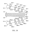
- FIGS. 3A and 3B are cross sections showing one exemplary embodiment of a method for fabricating the base 200 (including base 200-1 and 200-2) for the semiconductor package 500 of the invention.
- FIGS. 3A and 3B also illustrate how the first terminal surface of the conductive via can be aligned to the device-attach surface of the base.
- the method for fabricating bases for the semiconductor package 500 is also called a double-sided base fabricating process. Elements of the embodiments that are the same or similar as those previously described with reference to FIGS. 1-2 , are not repeated hereinafter for brevity.
- a carrier 400 with conductive seed layers 402a and 402b on the top surface 401 and the bottom surface 403 is provided.
- the carrier 400 may comprise FR4 glass epoxy or stainless steel.
- the conductive seed layers 402a and 402b are used as seed layers for subsequently formed conductive vias of bases.
- the conductive seed layers 402a and 402b may comprise copper.
- a laminating process is performed to respectively dispose a base material layer 406a and a base material layer 406b on the top surface 401 and the bottom surface 403 of the carrier 400, wherein the base material layer 406a and a base material layer 406b respectively cover the first conductive traces 404a and 404b.
- the laminating process of the base material layer 406a and the base material layer 406b is simultaneously performed on the top surface 401 and the bottom surface 403 of the carrier 400.
- the base material layer 406a and the base material layer 406b may include polypropylene (PP).
- the base material layer 406a includes a device-attach surface 201-1 and a solder-ball attach surface 203-1.
- the base material layer 406b includes a device-attach surface 201-2 and a solder-ball attach surface 203-2.
- the device-attach surfaces 201-1 and 201-2 are in contact with the conductive seed layers 402a and 402b, respectively.
- the solder-ball attach surfaces 203-1 and 203-2 are respectively opposite to the device-attach surfaces 201-1 and 201-2.
- the solder-ball attach surfaces 203-1 and 203-2 are away from the conductive seed layers 402a and 402b, respectively.
- a drilling process is performed to form openings (not shown) through the base material layer 406a and the base material layer 406b to define the positions of subsequently formed conductive vias 202-1, 202-2, 204-1, 204-2 206-1, 206-2, 208-1 and 208-2.
- the drilling process may comprise a laser drilling process, an etching drilling process or a mechanical drilling process.
- a plating process and an anisotropic etching process is performed to fill a conductive material into the openings to form the conductive vias 202-1, 204-1, 206-1, 208-1 through the base material layer 406a, and to form the conductive vias 202-2, 204-2, 206-2 and 208-2 through the base material layer 406b.
- the drilling process, the plating process and the anisotropic etching process are simultaneously performed on the base material layer 406a and the base material layer 406b.
- the plating process may comprise an electrical plating process.
- the conductive vias 202-1, 204-1, 206-1, 208-1 respectively have first terminal surfaces 202a-1, 204a-1, 206a-1 and 208a-1 and second terminal surfaces 202b-1, 204b-1, 206b-1 and 208b-1.
- the second terminal surfaces 202b-1, 204b-1, 206b-1 and 208b-1 are respectively opposite to the first terminal surfaces 202a-1, 204a-1, 206a-1 and 208a-1.
- the conductive vias 202-2, 204-2, 206-2, 208-2 respectively have first terminal surfaces 202a-2, 204a-2, 206a-2 and 208a-2, and second terminal surfaces 202b-2, 204b-2, 206b-2 and 208b-2.
- the second terminal surfaces 202b-2, 204b-2, 206b-2 and 208b-2 are respectively opposite to the first terminal surfaces 202a-2, 204a-2, 206a-2 and 208a-2.
- the device-attach surface 201-1 of the base material layer 406a and the device-attach surface 201-2 of the base material layer 406 are in contact with the conductive seed layers 402a and 402b, respectively. Therefore, the first terminal surfaces 202a-1, 204a-1, 206a-1 and 208a-1 of the conductive vias 202-1, 204-1, 206-1, 208-1 are aligned to the device-attach surface 201-1 of the base material layer 406a after performing the plating process and anisotropic etching process.
- the second terminal surfaces 202b-1, 204b-1, 206b-1 and 208b-1 are not required to be coplanar with the solder-ball attach surface 203-1 of the base material layer 406a.
- first terminal surfaces 202a-2, 204a-2, 206a-2 and 208a-2 of the conductive vias 202-2, 204-2, 206-2, 208-2 are aligned to the device-attach surface 201-2 of the base material layer 406b.
- the second terminal surfaces 202b-2, 204b-2, 206b-2 and 208b-2 are not required to be coplanar with the solder-ball attach surface 203-2 of the base material layer 406a.
- the base material layer 406a and the base material layer 406b are respectively separated from the top surface 401 and the bottom surface 403 of the carrier 400 to form bases 200-1 and 200-2, which are separated from each other.
- the conductive seed layers 402a and 402b are removed from the bases 200-1 and 200-2, respectively.
- first terminal surfaces 202a, 204a, 206a and 208a of the conductive vias 202, 204, 206, 208 are designed to be aligned to the device-attach surface 201 of the base 200.
- the first terminal surfaces 202a, 204a, 206a and 208a of the conductive vias 202, 204, 206, 208 can be provided the conductive structures 222, 224, 226 and 228, for example, copper pillar bumps, directly disposed thereon.
- the second terminal surfaces 202b, 204b, 206b and 208b of the conductive vias 202, 204, 206 and 208 are provided solder balls 212, 214, 216 and 218 disposed thereon, respectively.
- the semiconductor die 300 is mounted on the die attach surface 201 of the base 200 by the conductive structures 222, 224, 226 and 228 in accordance with some embodiments of the disclosure.
- an active surface of the semiconductor die 300 faces the base 200 by a bonding process.
- Circuits of the semiconductor die 300 are disposed on the active surface.
- pads 302, 304, 306, 308 are disposed on the top of the circuitry of the semiconductor die 300.
- the pads 302, 304, 306, 308 belong to the uppermost metal layer of the interconnection structure (not shown) of the semiconductor die 300.
- the pads 302, 304, 306, 308 are arranged in the central area of the first semiconductor die 310 to be used to transmit ground or power signals of the semiconductor die 300. Also, for the clear illustration of the relationship between the conductive structures 222, 224, 226 and 228 used for power or ground pads 302, 304, 306, 308 of the semiconductor die 300 and the conductive vias 202, 204, 206, 208 of the base 200, the conductive structures used for signal pads of the semiconductor dies are not shown in the figures ( FIGS. 1 and 2 ).
- a first passivation layer 310 is conformably formed covering the pads 302, 304, 306, 308 of the semiconductor die 300, in accordance with some embodiments of the disclosure.
- the first passivation layer 310 is formed by deposition and patterning processes.
- the first passivation layer 310 may be formed of materials including oxide, nitride, or oxynitride.
- the first passivation layer 310 has openings on the pads 302, 304, 306, 308 of the semiconductor die 300, so that a portion of the pads 302, 304, 306, 308 are respectively exposed from the openings.
- a second passivation layer 312 with openings therethrough is formed on the first passivation layer 310, as shown in FIG. 1 .
- the second passivation layer 312 is formed by a coating patterning and curing process.
- the second passivation layer 312 may comprise polyimide for providing reliable insulation when the semiconductor die 300 is subjected to various types of environmental stresses. A portion of each of the pads 302, 304, 306, 308 of the semiconductor die 300 is respectively exposed from the openings of the second passivation layer 312.
- the semiconductor package 500 uses the conductive structures 222, 224, 226 and 228 respectively connecting the power and ground pads of the semiconductor die 300 to the base 200 as shown in FIG. 1 (the conductive structures used for the signal pad of the semiconductor die are not shown in FIG. 1 ).
- each of the conductive structures may be a copper pillar bump structure composed of a metal stack comprising a UBM (under bump metallurgy) layer, a conductive pillar, a conductive buffer layer, and a solder cap.
- the conductive structures 222, 224, 226 and 228 are bump on trace (BOT) structures and rectangular in a plan view as shown in FIG. 2 .
- the conductive structures 222, 224, 226 and 228 can be designed to have other 180-degree rotationally symmetrical shapes, for example, an oval-shape or an octagonal shape.
- under bump metallurgy (UBM) layer patterns 314, 316, 318 and 320 of the conductive structure 222, 224, 226 and 228 are formed on the second passivation layer 312, which is disposed on the semiconductor die 300, in accordance with some embodiments of the disclosure.
- the UBM layer patterns 314, 316, 318 and 320 are formed by a deposition method such as a sputtering or plating method and a subsequent anisotropic etching process. The anisotropic etching process is performed after forming conductive pillars.
- the UBM layer patterns 314, 316, 318 and 320 line sidewalls and bottom surfaces of the openings of the second passivation layer 312. Also, the UBM layer patterns 314, 316, 318 and 320 extend over the top surface of the second passivation layer 312. In one embodiment, the UBM layer patterns 314, 316, 318 and 320 are composed of a Ti layer and a Cu layer on the Ti layer.
- conductive pillars 222a, 224a, 226a and 228a are respectively formed on the UBM layer patterns 314, 316, 318 and 320, in accordance with some embodiments of the disclosure.
- the conductive pillars 222a, 224a, 226a and 228a are separated from each other.
- the conductive pillars 222a, 224a, 226a and 228a respectively fill the openings of the second passivation layer 312 disposed on the semiconductor die 300. It should be noted that the conductive pillar and the UBM layer patterns within the same opening may form an integral plug of the resulting conductive structure.
- Formation positions of the conductive pillars 222a, 224a, 226a and 228a are defined by a dry film photoresist or liquid photoresist patterns (not shown).
- the conductive pillars 222a, 224a, 226a and 228a are used as solder joints for subsequent conductive structures, which are used to transmit ground or power signals of the semiconductor die 300, disposed thereon. Therefore, the conductive pillars 222a, 224a, 226a and 228a may help to increase the mechanical strength of the bump structure.
- the conductive pillars 222a, 224a, 226a and 228a may be formed of copper, so that deformation may be prevented during a subsequent solder re-flow process.
- conductive buffer layers 222b, 224b, 226b and 228b are respectively formed on the corresponding conductive pillars 222a, 224a, 226a and 228a, in accordance with some embodiments of the disclosure.
- the conductive buffer layers 222b, 224b, 226b and 228b are formed by an electroplating method.
- the conductive buffer layers 222b, 224b, 226b and 228b are optional elements serving as a seed layer, an adhesion layer and a barrier layer for subsequent conductive bumps formed thereon.
- the conductive buffer layers 222b, 224b, 226b and 228b may comprise Ni.
- the number of conductive buffer layers corresponds to the number of conductive pillars designed on the semiconductor die 300.
- solder caps 222c, 224c, 226c and 228c are respectively formed on the corresponding conductive buffer layers 222b, 224b, 226b and 228b, in accordance with some embodiments of the disclosure.
- the solder caps 222c, 224c, 226c and 228c are formed by electroplating a solder material with a patterned photoresist layer or by a screen printing process and a subsequent solder re-flow process.
- the UBM layer pattern 314, the conductive pillar 222a, the conductive buffer layers 222b (optional element), and solder cap 222c collectively form the conductive structure 222.
- the UBM layer pattern 316, the conductive pillar 224a, the conductive buffer layers 224b (optional element), and solder cap 224c collectively form the conductive structure 224.
- the UBM layer pattern 318, the conductive pillar 226a, the conductive buffer layers 226b (optional element), and solder cap 226c collectively form the conductive structure 226.
- the UBM layer pattern 320, the conductive pillar 228a, the conductive buffer layers 228b (optional element), and solder cap 228c collectively form the conductive structure 228.
- a solder resistance layer 230 is disposed on the base 200, away from an overlap region between the semiconductor die 300 and the base 200 as shown in FIG. 1 .
- the solder resistance layer 230 is formed by electroplating with a patterned photoresist layer or by a screen printing process.
- an underfill material or the underfill 232 can be introduced into the gap between the semiconductor die 300 and the base 200 as shown in FIG. 1 .
- the underfill 232 covers the conductive structures 224-228 and is adjacent to the solder resistance layer 230.
- the underfill 232 may comprise a capillary underfill (CUF), molded underfill (MUF) or a combination thereof.
- a molding compound 234 is formed covering the semiconductor die 300, the solder resistance layer 230, the underfill 232 and the device-attach surface 201 of the base 200 close to the semiconductor die 300.
- the molding material 234 may be formed of molding materials such as resin.
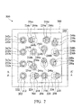
- FIG. 2 is a plan view of the semiconductor die 300 of the semiconductor package 500, in accordance with some embodiments of the disclosure. Also, FIG. 2 shows the relationship between the conductive structures and the conductive vias of the base of the semiconductor package, in accordance with some embodiments of the disclosure. FIG. 1 is also a cross-sectional view taken along line A-A' of FIG. 2 . It should be noted that for the clear illustration of the relationship between the conductive structures used for power or ground pads of the semiconductor die and the conductive vias of the base of the semiconductor package, the conductive structures and the conductive vias corresponding to the signal pads of the semiconductor die are not shown in FIG. 2 . Also, the solder resistance layer, the underfill and the molding compound of the semiconductor package 500 are not shown in FIG. 2 .
- the first terminal surfaces 202a, 204a, 206a and 208a of the conductive vias 202, 204, 206, 208 are designed to be aligned to the device-attach surface 201 of the base 200 according to the fabrication process, in accordance with some embodiments of the disclosure.
- the first terminal surfaces 202a, 204a, 206a and 208a of the conductive vias 202, 204, 206, 208 can be provided the conductive structures 222, 224, 226 and 228, for example, copper pillar bumps, directly disposed thereon.
- the first terminal surfaces 202a, 204a, 206a and 208a of the conductive vias 202, 204, 206, 208 also serve as interfaces between the conductive structures 222, 224, 226 and 228 and the conductive vias 202, 204, 206, 208, respectively.
- the second terminal surfaces 202b, 204b, 206b and 208b of the conductive vias 202, 204, 206 and 208 are provided solder balls 212, 214, 216 and 218 directly disposed thereon, respectively.
- the second terminal surfaces 202b, 204b, 206b and 208b of the conductive vias 202a, 204a, 206a and 208a may also serve as interfaces between the conductive vias 202, 204, 206, 208 and the solder balls 212, 214, 216 and 218.
- the conductive vias of the base 200 are defined as extending only along a direction substantially vertical to the device-attach surface 201 and the solder-ball attach surface 203 of the base 200 as shown in FIGS. 1 and 2 .
- the terminal surfaces of the conductive vias, which are close to the device-attach surface 201 of the base 200, do not have any redistribution routing function. That is to say, the conductive via plugs of the base 200 do not have any segments extending substantially along the device-attach surface 201 of the base 200.
- no conductive pad is disposed on the base, covering the terminal surface of the conductive via, which is close to the device-attach surface 201 of the base 200.
- the first terminal surfaces 202a, 204a, 206a and 208a respectively fully overlap with the second terminal surfaces 202b, 204b, 206b and 208b of the conductive vias 202, 204, 206 and 208 in a cross-sectional view as shown in FIG. 1 and in a plan view as shown in FIG. 2 .
- first terminal surfaces of the conductive vias 232a-232c, 234a-234c, 236a-236c and 238a-238c which are provided conductive structures 242a-242c, 244a-244c, 246a-246c and 248a-248c directly disposed thereon, are designed to fully overlap with second terminal surfaces of the conductive vias 232a-232c, 254a-234c, 236a-236c and 238a-238c, which are provided the solder balls 252a-252c, 254a-254c, 256a-256c and 258a-258c disposed thereon, respectively, in accordance with some embodiments of the disclosure as shown in FIG. 2 .
- the conductive structures of the semiconductor package 500 can be designed to fully or partially overlap with the corresponding conductive vias of the base 200 in a cross-sectional view as shown in FIG. 1 and in a plan view as shown in FIG. 2 .
- the arrangement of the conductive structures is not limited by the positions of the corresponding conductive vias of the base.
- the conductive structures are not required to be disposed spaced apart from the corresponding conductive vias of the base. Therefore, the input/output (I/O) connection counts of the semiconductor die 300 and the conductive via counts of the base 200 can be improved, a high-density semiconductor package is achieved.
- the conductive structures 222, 226, 242a, 242b, 242c, 244b are designed to fully overlap with the corresponding conductive vias 202, 206, 232a, 232b, 232c, 234b of the base 200 as shown in FIGS. 1 and 2 .
- the conductive structures 224, 228, 244a, 244c, 246a-246c, 248a-248c are designed to partially overlap with the corresponding conductive vias 204, 208, 234a, 234c, 236a-236c, 238a-238c of the base 200 as shown in FIGS. 1 and 2 .
- the conductive vias of the base 200 are designed to fully overlap with the corresponding solder balls on the base 200 in a cross-sectional view as shown in FIG. 1 and in a plan view as shown in FIG. 2 . Therefore, the conductive structures of the semiconductor package 500 can be designed to fully overlap or partially overlap the corresponding solder balls, in accordance with some embodiments of the disclosure as shown in FIGS. 1 and 2 .
- the conductive structures 222, 226, 242a, 242b, 242c, 244b are designed to fully overlap with the corresponding solder balls 212, 216, 252a, 252b, 252c, 254b on the base 200 as shown in FIGS. 1 and 2 .
- the conductive structures 224, 228, 244a, 244c, 246a-246c, 248a-248c are designed to partially overlap with the corresponding conductive vias 214, 218, 254a, 254c, 256a-256c, 258a-258c on the base 200 as shown in FIGS. 1 and 2 .
- Embodiments provide a semiconductor package.
- the semiconductor die of the semiconductor package connects to the base using conductive structures, which is in contact with the corresponding conductive vias passing through the base.
- the conductive structures are designed to connect to power or ground pads of the semiconductor die.
- the interface between the conductive structure and the corresponding conductive via is aligned to the device-attach surface of the base.
- the conductive structure can be designed to be in contact with the corresponding conductive via without any conductive pad or redistribution pattern.
- the arrangement of the conductive structures is not limited by the positions of the corresponding conductive vias of the base.
- the input/output (I/O) connection counts of the semiconductor die and the conductive via counts of the base can be improved, and a high-density semiconductor package is achieved.
- the semiconductor package may have improved the voltage drop across the network in the package.
- the heat generated from the semiconductor die can be quickly dissipated to the outside due to the shortened path (The conductive structure can be design to be in contact with the corresponding conductive via without any conductive pad or redistribution pattern).
- the thermal performance of the semiconductor package can be improved.
Landscapes
- Wire Bonding (AREA)
- Internal Circuitry In Semiconductor Integrated Circuit Devices (AREA)
- Physics & Mathematics (AREA)
- Geometry (AREA)
Abstract
Description
- The present invention relates to a semiconductor package, and in particular relates to a base design for a high-density semiconductor package.
- For a semiconductor chip package design, an increased number of input/output (I/O) connections for multi-functional chips is required. The impact of this will be pressure on printed circuit board (PCB) fabricators to minimize linewidth and space or to develop direct chip attach (DCA) semiconductors. However, the increased number of input/output connections of a multi-functional chip package may induce thermal electrical problems, for such as, problems with heat dissipation, cross talk, signal propagation delay, electromagnetic interference in RF circuits, etc. The thermal electrical problems may affect the reliability and quality of products.
- Thus, a novel semiconductor package is desirable.
- A semiconductor package is provided. An exemplary embodiment of a semiconductor package includes a base having a device-attach surface and a solder-ball attach surface opposite to the device-attach surface. A conductive via passes through the base. A semiconductor die is mounted on the base by a conductive structure. The conductive structure is in contact with the first terminal surface of the conductive via.
- Another exemplary embodiment of a semiconductor package includes a base having a device-attach surface. A conductive via passes through the base. A semiconductor die is mounted on the base. The semiconductor die is in contact with the conductive structure by a conductive structure.
- Yet another exemplary embodiment of a semiconductor package includes a conductive via passes through a base. The conductive via has a first terminal surface and a second terminal surface opposite to the first terminal surface. A semiconductor die is in contact with a first terminal surface of the conductive via by a conductive structure. A solder-ball is in contact with a second terminal surface of the conductive via. The second terminal surface is opposite to the first terminal surface.
- A detailed description is given in the following embodiments with reference to the accompanying drawings.
- The present invention can be more fully understood by reading the subsequent detailed description and examples with references made to the accompanying drawings, wherein:
-
FIG. 1 is a cross-sectional view of a semiconductor package in accordance with some embodiments of the disclosure. -
FIG. 2 is a plan view of a semiconductor die of a semiconductor package, showing the relationship between the conductive structures of the semiconductor die and the conductive vias of the base of the semiconductor package, in accordance with some embodiments of the disclosure. -
FIGS. 3A and3B are cross sections showing one exemplary embodiment of a method for fabricating a base for a semiconductor package of the invention. - The following description is of the best-contemplated mode of carrying out the invention. This description is made for the purpose of illustrating the general principles of the invention and should not be taken in a limiting sense. The scope of the invention is determined by reference to the appended claims.
- The present invention will be described with respect to particular embodiments and with reference to certain drawings, but the invention is not limited thereto and is only limited by the claims. The drawings described are only schematic and are non-limiting. In the drawings, the size of some of the elements may be exaggerated for illustrative purposes and not drawn to scale. The dimensions and the relative dimensions do not correspond to actual dimensions in the practice of the invention.
-
FIG. 1 is a cross-sectional view of asemiconductor package 500 in accordance with some embodiments of the disclosure. In some embodiments, thesemiconductor package 500 can be a flip chip package using conductive structures, for example, copper pillar bumps, connecting a semiconductor device to a base. As illustrated inFIG. 1 , thesemiconductor package 500 includes abase 200, a semiconductor die 300 andconductive structures - In some embodiments as shown in
FIG. 1 , thebase 200 includes a device-attach surface 201 and a solder-ball attach surface 203 opposite to the device-attach surface 201. In some embodiments, thebase 200, for example a printed circuit board (PCB), may be a substrate which formed of polypropylene (PP). In some embodiments, a plurality ofconductive vias base 200. As shown inFIG. 1 , the conductive via 202 includes afirst terminal surface 202a and asecond terminal surface 202b opposite to thefirst terminal surface 202a in accordance with some embodiments of the disclosure. - In some embodiments, the
first terminal surface 202a of the conductive via 202 may be aligned to the device-attach surface 201 of thebase 200. In some embodiments, thesecond terminal surface 202b of the conductive via 202 is not coplanar with the device-attach surface 201 of thebase 200. Similarly, the firstterminal surfaces conductive vias attach surface 201 of thebase 200, respectively.Second terminal surfaces conductive vias attach surface 201 of thebase 200. In some other embodiments, additional metal films may be plated on thefirst terminal surface first terminal surface attach surface 201 of thebase 200. -
FIGS. 3A and3B are cross sections showing one exemplary embodiment of a method for fabricating the base 200 (including base 200-1 and 200-2) for thesemiconductor package 500 of the invention.FIGS. 3A and3B also illustrate how the first terminal surface of the conductive via can be aligned to the device-attach surface of the base. In some embodiments, the method for fabricating bases for thesemiconductor package 500 is also called a double-sided base fabricating process. Elements of the embodiments that are the same or similar as those previously described with reference toFIGS. 1-2 , are not repeated hereinafter for brevity. As shown inFIG. 3A , acarrier 400 withconductive seed layers top surface 401 and thebottom surface 403 is provided. In some embodiments, thecarrier 400 may comprise FR4 glass epoxy or stainless steel. Also, theconductive seed layers conductive seed layers - Next, as shown in
FIG. 3A , a laminating process is performed to respectively dispose abase material layer 406a and abase material layer 406b on thetop surface 401 and thebottom surface 403 of thecarrier 400, wherein thebase material layer 406a and abase material layer 406b respectively cover the first conductive traces 404a and 404b. In some embodiments, the laminating process of thebase material layer 406a and thebase material layer 406b is simultaneously performed on thetop surface 401 and thebottom surface 403 of thecarrier 400. In some embodiments, thebase material layer 406a and thebase material layer 406b may include polypropylene (PP). In some embodiments, thebase material layer 406a includes a device-attach surface 201-1 and a solder-ball attach surface 203-1. Similarly, thebase material layer 406b includes a device-attach surface 201-2 and a solder-ball attach surface 203-2. As shown inFIG. 3A , the device-attach surfaces 201-1 and 201-2 are in contact with theconductive seed layers conductive seed layers - Next, please refer to
FIG. 3A again, wherein a drilling process is performed to form openings (not shown) through thebase material layer 406a and thebase material layer 406b to define the positions of subsequently formed conductive vias 202-1, 202-2, 204-1, 204-2 206-1, 206-2, 208-1 and 208-2. In some embodiments, the drilling process may comprise a laser drilling process, an etching drilling process or a mechanical drilling process. Next, a plating process and an anisotropic etching process is performed to fill a conductive material into the openings to form the conductive vias 202-1, 204-1, 206-1, 208-1 through thebase material layer 406a, and to form the conductive vias 202-2, 204-2, 206-2 and 208-2 through thebase material layer 406b. In some embodiments, the drilling process, the plating process and the anisotropic etching process are simultaneously performed on thebase material layer 406a and thebase material layer 406b. In some embodiments, the plating process may comprise an electrical plating process. - As shown in
FIG. 3A , the conductive vias 202-1, 204-1, 206-1, 208-1 respectively have firstterminal surfaces 202a-1, 204a-1, 206a-1 and 208a-1 and second terminal surfaces 202b-1, 204b-1, 206b-1 and 208b-1. The second terminal surfaces 202b-1, 204b-1, 206b-1 and 208b-1 are respectively opposite to the firstterminal surfaces 202a-1, 204a-1, 206a-1 and 208a-1. Similarly, the conductive vias 202-2, 204-2, 206-2, 208-2 respectively have firstterminal surfaces 202a-2, 204a-2, 206a-2 and 208a-2, and second terminal surfaces 202b-2, 204b-2, 206b-2 and 208b-2. The second terminal surfaces 202b-2, 204b-2, 206b-2 and 208b-2 are respectively opposite to the firstterminal surfaces 202a-2, 204a-2, 206a-2 and 208a-2. - As shown in
FIG. 3A , the device-attach surface 201-1 of thebase material layer 406a and the device-attach surface 201-2 of the base material layer 406 are in contact with theconductive seed layers terminal surfaces 202a-1, 204a-1, 206a-1 and 208a-1 of the conductive vias 202-1, 204-1, 206-1, 208-1 are aligned to the device-attach surface 201-1 of thebase material layer 406a after performing the plating process and anisotropic etching process. The second terminal surfaces 202b-1, 204b-1, 206b-1 and 208b-1 are not required to be coplanar with the solder-ball attach surface 203-1 of thebase material layer 406a. Similarly, the firstterminal surfaces 202a-2, 204a-2, 206a-2 and 208a-2 of the conductive vias 202-2, 204-2, 206-2, 208-2 are aligned to the device-attach surface 201-2 of thebase material layer 406b. The second terminal surfaces 202b-2, 204b-2, 206b-2 and 208b-2 are not required to be coplanar with the solder-ball attach surface 203-2 of thebase material layer 406a. - Next, as shown in
FIG. 3B , thebase material layer 406a and thebase material layer 406b are respectively separated from thetop surface 401 and thebottom surface 403 of thecarrier 400 to form bases 200-1 and 200-2, which are separated from each other. Next, as shown inFIG. 3B , again, theconductive seed layers - Please return to
FIG. 1 , because the firstterminal surfaces conductive vias surface 201 of thebase 200. The firstterminal surfaces conductive vias conductive structures terminal surfaces conductive vias solder balls - As shown in
FIG. 1 , the semiconductor die 300 is mounted on the die attachsurface 201 of the base 200 by theconductive structures base 200 by a bonding process. Circuits of the semiconductor die 300 are disposed on the active surface. In some embodiments,pads pads pads conductive structures ground pads conductive vias base 200, the conductive structures used for signal pads of the semiconductor dies are not shown in the figures (FIGS. 1 and2 ). - As shown in
FIG. 1 , afirst passivation layer 310 is conformably formed covering thepads first passivation layer 310 is formed by deposition and patterning processes. In some embodiments, thefirst passivation layer 310 may be formed of materials including oxide, nitride, or oxynitride. In some embodiments, thefirst passivation layer 310 has openings on thepads pads - In some embodiments, a
second passivation layer 312 with openings therethrough is formed on thefirst passivation layer 310, as shown inFIG. 1 . In some embodiments, thesecond passivation layer 312 is formed by a coating patterning and curing process. In some embodiments, thesecond passivation layer 312 may comprise polyimide for providing reliable insulation when the semiconductor die 300 is subjected to various types of environmental stresses. A portion of each of thepads second passivation layer 312. - In some embodiments, the
semiconductor package 500 uses theconductive structures FIG. 1 (the conductive structures used for the signal pad of the semiconductor die are not shown inFIG. 1 ). In some embodiments, each of the conductive structures may be a copper pillar bump structure composed of a metal stack comprising a UBM (under bump metallurgy) layer, a conductive pillar, a conductive buffer layer, and a solder cap. In some embodiments, theconductive structures FIG. 2 . In some other embodiments, theconductive structures - As shown in
FIG. 1 , under bump metallurgy (UBM)layer patterns conductive structure second passivation layer 312, which is disposed on the semiconductor die 300, in accordance with some embodiments of the disclosure. In some embodiments, theUBM layer patterns UBM layer patterns second passivation layer 312. Also, theUBM layer patterns second passivation layer 312. In one embodiment, theUBM layer patterns - As shown in
FIG. 1 ,conductive pillars UBM layer patterns conductive pillars conductive pillars second passivation layer 312 disposed on the semiconductor die 300. It should be noted that the conductive pillar and the UBM layer patterns within the same opening may form an integral plug of the resulting conductive structure. Formation positions of theconductive pillars conductive pillars conductive pillars conductive pillars - As shown in
FIG. 1 , conductive buffer layers 222b, 224b, 226b and 228b are respectively formed on the correspondingconductive pillars - As shown in
FIG. 1 , solder caps 222c, 224c, 226c and 228c are respectively formed on the corresponding conductive buffer layers 222b, 224b, 226b and 228b, in accordance with some embodiments of the disclosure. In some embodiments, the solder caps 222c, 224c, 226c and 228c are formed by electroplating a solder material with a patterned photoresist layer or by a screen printing process and a subsequent solder re-flow process. As shown inFIG. 1 , theUBM layer pattern 314, theconductive pillar 222a, the conductive buffer layers 222b (optional element), andsolder cap 222c collectively form theconductive structure 222. TheUBM layer pattern 316, theconductive pillar 224a, the conductive buffer layers 224b (optional element), andsolder cap 224c collectively form theconductive structure 224. TheUBM layer pattern 318, theconductive pillar 226a, the conductive buffer layers 226b (optional element), andsolder cap 226c collectively form theconductive structure 226. TheUBM layer pattern 320, theconductive pillar 228a, the conductive buffer layers 228b (optional element), andsolder cap 228c collectively form theconductive structure 228. - In some embodiments, a
solder resistance layer 230 is disposed on thebase 200, away from an overlap region between the semiconductor die 300 and the base 200 as shown inFIG. 1 . In some embodiments, thesolder resistance layer 230 is formed by electroplating with a patterned photoresist layer or by a screen printing process. - In some embodiments, an underfill material or the
underfill 232 can be introduced into the gap between the semiconductor die 300 and the base 200 as shown inFIG. 1 . Theunderfill 232 covers the conductive structures 224-228 and is adjacent to thesolder resistance layer 230. In some embodiments, theunderfill 232 may comprise a capillary underfill (CUF), molded underfill (MUF) or a combination thereof. - As shown in
FIG. 1 , amolding compound 234 is formed covering the semiconductor die 300, thesolder resistance layer 230, theunderfill 232 and the device-attachsurface 201 of the base 200 close to the semiconductor die 300. In some embodiments, themolding material 234 may be formed of molding materials such as resin. -
FIG. 2 is a plan view of the semiconductor die 300 of thesemiconductor package 500, in accordance with some embodiments of the disclosure. Also,FIG. 2 shows the relationship between the conductive structures and the conductive vias of the base of the semiconductor package, in accordance with some embodiments of the disclosure.FIG. 1 is also a cross-sectional view taken along line A-A' ofFIG. 2 . It should be noted that for the clear illustration of the relationship between the conductive structures used for power or ground pads of the semiconductor die and the conductive vias of the base of the semiconductor package, the conductive structures and the conductive vias corresponding to the signal pads of the semiconductor die are not shown inFIG. 2 . Also, the solder resistance layer, the underfill and the molding compound of thesemiconductor package 500 are not shown inFIG. 2 . - As shown in
FIGS. 1 and2 , the firstterminal surfaces conductive vias surface 201 of the base 200 according to the fabrication process, in accordance with some embodiments of the disclosure. The firstterminal surfaces conductive vias conductive structures terminal surfaces conductive vias conductive structures conductive vias terminal surfaces conductive vias solder balls terminal surfaces conductive vias conductive vias solder balls - In some embodiments, the conductive vias of the base 200 are defined as extending only along a direction substantially vertical to the device-attach
surface 201 and the solder-ball attachsurface 203 of the base 200 as shown inFIGS. 1 and2 . The terminal surfaces of the conductive vias, which are close to the device-attachsurface 201 of thebase 200, do not have any redistribution routing function. That is to say, the conductive via plugs of the base 200 do not have any segments extending substantially along the device-attachsurface 201 of thebase 200. In some embodiments, no conductive pad is disposed on the base, covering the terminal surface of the conductive via, which is close to the device-attachsurface 201 of thebase 200. That is to say, there is no conductive pad disposed between the conductive structure and the conductive via passing through thebase 200. In some embodiments, the firstterminal surfaces terminal surfaces conductive vias FIG. 1 and in a plan view as shown inFIG. 2 . Similarly, first terminal surfaces of the conductive vias 232a-232c, 234a-234c, 236a-236c and 238a-238c, which are providedconductive structures 242a-242c, 244a-244c, 246a-246c and 248a-248c directly disposed thereon, are designed to fully overlap with second terminal surfaces of the conductive vias 232a-232c, 254a-234c, 236a-236c and 238a-238c, which are provided thesolder balls 252a-252c, 254a-254c, 256a-256c and 258a-258c disposed thereon, respectively, in accordance with some embodiments of the disclosure as shown inFIG. 2 . - In some embodiments, the conductive structures of the
semiconductor package 500 can be designed to fully or partially overlap with the corresponding conductive vias of the base 200 in a cross-sectional view as shown inFIG. 1 and in a plan view as shown inFIG. 2 . The arrangement of the conductive structures is not limited by the positions of the corresponding conductive vias of the base. For example, the conductive structures are not required to be disposed spaced apart from the corresponding conductive vias of the base. Therefore, the input/output (I/O) connection counts of the semiconductor die 300 and the conductive via counts of the base 200 can be improved, a high-density semiconductor package is achieved. For example, theconductive structures conductive vias FIGS. 1 and2 . For example, theconductive structures conductive vias FIGS. 1 and2 . - In some embodiments, the conductive vias of the base 200 are designed to fully overlap with the corresponding solder balls on the base 200 in a cross-sectional view as shown in
FIG. 1 and in a plan view as shown inFIG. 2 . Therefore, the conductive structures of thesemiconductor package 500 can be designed to fully overlap or partially overlap the corresponding solder balls, in accordance with some embodiments of the disclosure as shown inFIGS. 1 and2 . For example, theconductive structures corresponding solder balls FIGS. 1 and2 . For example, theconductive structures conductive vias FIGS. 1 and2 . - Embodiments provide a semiconductor package. The semiconductor die of the semiconductor package connects to the base using conductive structures, which is in contact with the corresponding conductive vias passing through the base. The conductive structures are designed to connect to power or ground pads of the semiconductor die. According to the design of the base, the interface between the conductive structure and the corresponding conductive via is aligned to the device-attach surface of the base. The conductive structure can be designed to be in contact with the corresponding conductive via without any conductive pad or redistribution pattern. The arrangement of the conductive structures is not limited by the positions of the corresponding conductive vias of the base. The input/output (I/O) connection counts of the semiconductor die and the conductive via counts of the base can be improved, and a high-density semiconductor package is achieved. Also, the semiconductor package may have improved the voltage drop across the network in the package. Also, the heat generated from the semiconductor die can be quickly dissipated to the outside due to the shortened path (The conductive structure can be design to be in contact with the corresponding conductive via without any conductive pad or redistribution pattern). The thermal performance of the semiconductor package can be improved.
- While the invention has been described by way of example and in terms of the preferred embodiments, it is to be understood that the invention is not limited to the disclosed embodiments. On the contrary, it is intended to cover various modifications and similar arrangements (as would be apparent to those skilled in the art). Therefore, the scope of the appended claims should be accorded the broadest interpretation so as to encompass all such modifications and similar arrangements.
Claims (12)
- A semiconductor package (500), comprising:a base (200) having a device-attach surface (201);a conductive via (202, 204, 206, 208) passing through the base; anda semiconductor die (300) mounted on the base by a conductive structure (222, 224, 226, 228), wherein the conductive structure is in contact with a first terminal surface (202a, 204a, 206a, 208a) of the conductive via.
- The semiconductor package as claimed in claim 1, wherein the base has a solder-ball attach surface (203) opposite to the device-attach surface, wherein the solder-ball attach surface is away from the semiconductor die.
- The semiconductor package as claimed in claim 2, wherein the conductive via comprises a second terminal surface (202b, 204b, 206b, 208b) opposite to the first terminal surface, wherein first terminal surface aligned to the device-attach surface, and the second terminal surface is away from the semiconductor die.
- The semiconductor package as claimed in claim 3, wherein the second terminal surface of the conductive via is not coplanar with the solder-ball attach surface of the base.
- The semiconductor package as claimed in any of claims 3 to 4, wherein the conductive structure fully overlaps with the conductive via.
- The semiconductor package as claimed in any of claims 3 to 5, wherein the conductive structure partially overlaps with the conductive via.
- The semiconductor package as claimed in any of claims 3 to 6, further comprising:a solder ball (212, 214, 216, 218) disposed on the solder-ball attach surface of the base and in contact with the second terminal surface of the conductive via.
- The semiconductor package as claimed in claim 7, wherein a first interface between the conductive structure and the conductive via conductive via is aligned to the device-attach surface of the base, and a second interface between the conductive via and the solder ball is opposite to the first interface, wherein the second interface is not coplanar with the solder-ball attach surface of the base.
- The semiconductor package as claimed in claim any of claims 7 to 8, wherein the solder ball overlaps with the conductive structure of the semiconductor die.
- The semiconductor package as claimed in any of claims 7 to 9, wherein the solder ball fully overlaps with the conductive via.
- The semiconductor package as claimed in any of claims 1 to 10, wherein the conductive structure of the semiconductor die is coupled to a power pad or ground pad of the semiconductor die.
- The semiconductor package as claimed in any of claims 1 to 11, wherein the conductive structure of the semiconductor die is a bump on trace structure and rectangular in a plan view.
Applications Claiming Priority (1)
| Application Number | Priority Date | Filing Date | Title |
|---|---|---|---|
| US14/535,643 US9972593B2 (en) | 2014-11-07 | 2014-11-07 | Semiconductor package |
Publications (2)
| Publication Number | Publication Date |
|---|---|
| EP3024026A1 true EP3024026A1 (en) | 2016-05-25 |
| EP3024026B1 EP3024026B1 (en) | 2019-09-18 |
Family
ID=53002551
Family Applications (1)
| Application Number | Title | Priority Date | Filing Date |
|---|---|---|---|
| EP15164798.9A Active EP3024026B1 (en) | 2014-11-07 | 2015-04-23 | Semiconductor package |
Country Status (4)
| Country | Link |
|---|---|
| US (2) | US9972593B2 (en) |
| EP (1) | EP3024026B1 (en) |
| CN (1) | CN106206500B (en) |
| TW (1) | TWI636536B (en) |
Families Citing this family (7)
| Publication number | Priority date | Publication date | Assignee | Title |
|---|---|---|---|---|
| US9972593B2 (en) | 2014-11-07 | 2018-05-15 | Mediatek Inc. | Semiconductor package |
| US10410988B2 (en) * | 2016-08-09 | 2019-09-10 | Semtech Corporation | Single-shot encapsulation |
| US10304792B1 (en) * | 2017-11-16 | 2019-05-28 | Futurewei Technologies, Inc. | Semiconductor package having reduced internal power pad pitch |
| TWI697078B (en) * | 2018-08-03 | 2020-06-21 | 欣興電子股份有限公司 | Package substrate structure and method of bonding using the same |
| US20200051925A1 (en) * | 2018-08-13 | 2020-02-13 | Mediatek Inc. | Semiconductor device with an em-integrated damper |
| US20240178126A1 (en) * | 2021-03-30 | 2024-05-30 | Virginia Tech Intellectual Properties, Inc. | Double-side cooled power modules |
| TWI869154B (en) * | 2024-01-05 | 2025-01-01 | 慧隆科技股份有限公司 | Advanced Semiconductor Package Structure |
Citations (7)
| Publication number | Priority date | Publication date | Assignee | Title |
|---|---|---|---|---|
| JP2004007024A (en) * | 2003-10-02 | 2004-01-08 | Matsushita Electric Ind Co Ltd | Semiconductor device |
| US20060186524A1 (en) * | 2005-02-18 | 2006-08-24 | Fujitsu Limited | Semiconductor device |
| US20090289362A1 (en) * | 2008-05-21 | 2009-11-26 | Texas Instruments Incorporated | Low Inductance Ball Grid Array Device Having Chip Bumps on Substrate Vias |
| US20120032314A1 (en) * | 2008-05-27 | 2012-02-09 | Nan-Cheng Chen | Package-on-package with fan-out wlcsp |
| US20120286416A1 (en) * | 2011-05-11 | 2012-11-15 | Tessera Research Llc | Semiconductor chip package assembly and method for making same |
| US20130221536A1 (en) * | 2012-02-29 | 2013-08-29 | Thomas Matthew Gregorich | Enhanced flip chip structure using copper column interconnect |
| US20140153210A1 (en) * | 2012-12-03 | 2014-06-05 | Invensas Corporation | Advanced device assembly structures and methods |
Family Cites Families (16)
| Publication number | Priority date | Publication date | Assignee | Title |
|---|---|---|---|---|
| US6054767A (en) * | 1998-01-13 | 2000-04-25 | Lsi Logic Corp. | Programmable substrate for array-type packages |
| US20030047348A1 (en) * | 2001-09-10 | 2003-03-13 | Rebecca Jessep | Grid array mounting arrangements |
| JP4344752B2 (en) | 2007-01-25 | 2009-10-14 | ソニー株式会社 | Manufacturing method of semiconductor device |
| US20090321119A1 (en) * | 2008-06-30 | 2009-12-31 | Yasuhiro Kohara | Device mounting board, semiconductor module, mobile device, and manufacturing method of device mounting board |
| KR101632399B1 (en) * | 2009-10-26 | 2016-06-23 | 삼성전자주식회사 | Semiconductor and method for fabricating the same |
| US9607936B2 (en) * | 2009-10-29 | 2017-03-28 | Taiwan Semiconductor Manufacturing Company, Ltd. | Copper bump joint structures with improved crack resistance |
| US20110133327A1 (en) * | 2009-12-09 | 2011-06-09 | Hung-Hsin Hsu | Semiconductor package of metal post solder-chip connection |
| FI20105493A0 (en) | 2010-05-07 | 2010-05-07 | Polar Electro Oy | Power transmission |
| US20120187545A1 (en) * | 2011-01-24 | 2012-07-26 | Broadcom Corporation | Direct through via wafer level fanout package |
| US8367475B2 (en) * | 2011-03-25 | 2013-02-05 | Broadcom Corporation | Chip scale package assembly in reconstitution panel process format |
| US8552540B2 (en) * | 2011-05-10 | 2013-10-08 | Conexant Systems, Inc. | Wafer level package with thermal pad for higher power dissipation |
| US8772943B2 (en) * | 2011-12-07 | 2014-07-08 | Stmicroelectronics Pte Ltd. | Offset of contact opening for copper pillars in flip chip packages |
| TWI562295B (en) * | 2012-07-31 | 2016-12-11 | Mediatek Inc | Semiconductor package and method for fabricating base for semiconductor package |
| KR101397668B1 (en) | 2012-12-27 | 2014-05-23 | 전자부품연구원 | A transmitting antenna and a transmitter for wireless power charging |
| US9165877B2 (en) * | 2013-10-04 | 2015-10-20 | Mediatek Inc. | Fan-out semiconductor package with copper pillar bumps |
| US9972593B2 (en) | 2014-11-07 | 2018-05-15 | Mediatek Inc. | Semiconductor package |
-
2014
- 2014-11-07 US US14/535,643 patent/US9972593B2/en active Active
-
2015
- 2015-04-23 EP EP15164798.9A patent/EP3024026B1/en active Active
- 2015-04-27 TW TW104113351A patent/TWI636536B/en active
- 2015-06-17 CN CN201510337270.6A patent/CN106206500B/en active Active
-
2018
- 2018-04-10 US US15/949,868 patent/US10312210B2/en active Active
Patent Citations (7)
| Publication number | Priority date | Publication date | Assignee | Title |
|---|---|---|---|---|
| JP2004007024A (en) * | 2003-10-02 | 2004-01-08 | Matsushita Electric Ind Co Ltd | Semiconductor device |
| US20060186524A1 (en) * | 2005-02-18 | 2006-08-24 | Fujitsu Limited | Semiconductor device |
| US20090289362A1 (en) * | 2008-05-21 | 2009-11-26 | Texas Instruments Incorporated | Low Inductance Ball Grid Array Device Having Chip Bumps on Substrate Vias |
| US20120032314A1 (en) * | 2008-05-27 | 2012-02-09 | Nan-Cheng Chen | Package-on-package with fan-out wlcsp |
| US20120286416A1 (en) * | 2011-05-11 | 2012-11-15 | Tessera Research Llc | Semiconductor chip package assembly and method for making same |
| US20130221536A1 (en) * | 2012-02-29 | 2013-08-29 | Thomas Matthew Gregorich | Enhanced flip chip structure using copper column interconnect |
| US20140153210A1 (en) * | 2012-12-03 | 2014-06-05 | Invensas Corporation | Advanced device assembly structures and methods |
Also Published As
| Publication number | Publication date |
|---|---|
| CN106206500B (en) | 2019-04-12 |
| EP3024026B1 (en) | 2019-09-18 |
| US20180233476A1 (en) | 2018-08-16 |
| US10312210B2 (en) | 2019-06-04 |
| TW201618257A (en) | 2016-05-16 |
| US20160133594A1 (en) | 2016-05-12 |
| CN106206500A (en) | 2016-12-07 |
| US9972593B2 (en) | 2018-05-15 |
| TWI636536B (en) | 2018-09-21 |
Similar Documents
| Publication | Publication Date | Title |
|---|---|---|
| EP3024026B1 (en) | Semiconductor package | |
| US11469201B2 (en) | Semiconductor package and method for fabricating base for semiconductor package | |
| US9177899B2 (en) | Semiconductor package and method for fabricating base for semiconductor package | |
| US10109608B2 (en) | Semiconductor package | |
| US20160043041A1 (en) | Semiconductor packages and methods of packaging semiconductor devices | |
| US10916449B2 (en) | Semiconductor package and method for fabricating base for semiconductor package | |
| US10483196B2 (en) | Embedded trace substrate structure and semiconductor package structure including the same | |
| US20160358877A1 (en) | Semiconductor package using flip-chip technology | |
| KR102826729B1 (en) | Semiconductor device and manufacturing method thereof | |
| US10276465B2 (en) | Semiconductor package assembly | |
| US9408313B2 (en) | Packaging substrate and method of fabricating the same | |
| KR101538544B1 (en) | Substrate for semiconductor device, fabricating method thereof and semiconductor device package comprising the substrate |
Legal Events
| Date | Code | Title | Description |
|---|---|---|---|
| AK | Designated contracting states |
Kind code of ref document: A1 Designated state(s): AL AT BE BG CH CY CZ DE DK EE ES FI FR GB GR HR HU IE IS IT LI LT LU LV MC MK MT NL NO PL PT RO RS SE SI SK SM TR |
|
| AX | Request for extension of the european patent |
Extension state: BA ME |
|
| PUAI | Public reference made under article 153(3) epc to a published international application that has entered the european phase |
Free format text: ORIGINAL CODE: 0009012 |
|
| 17P | Request for examination filed |
Effective date: 20160920 |
|
| RBV | Designated contracting states (corrected) |
Designated state(s): AL AT BE BG CH CY CZ DE DK EE ES FI FR GB GR HR HU IE IS IT LI LT LU LV MC MK MT NL NO PL PT RO RS SE SI SK SM TR |
|
| STAA | Information on the status of an ep patent application or granted ep patent |
Free format text: STATUS: EXAMINATION IS IN PROGRESS |
|
| 17Q | First examination report despatched |
Effective date: 20180710 |
|
| GRAP | Despatch of communication of intention to grant a patent |
Free format text: ORIGINAL CODE: EPIDOSNIGR1 |
|
| STAA | Information on the status of an ep patent application or granted ep patent |
Free format text: STATUS: GRANT OF PATENT IS INTENDED |
|
| INTG | Intention to grant announced |
Effective date: 20190306 |
|
| GRAS | Grant fee paid |
Free format text: ORIGINAL CODE: EPIDOSNIGR3 |
|
| RAP1 | Party data changed (applicant data changed or rights of an application transferred) |
Owner name: MEDIATEK INC. |
|
| GRAA | (expected) grant |
Free format text: ORIGINAL CODE: 0009210 |
|
| STAA | Information on the status of an ep patent application or granted ep patent |
Free format text: STATUS: THE PATENT HAS BEEN GRANTED |
|
| AK | Designated contracting states |
Kind code of ref document: B1 Designated state(s): AL AT BE BG CH CY CZ DE DK EE ES FI FR GB GR HR HU IE IS IT LI LT LU LV MC MK MT NL NO PL PT RO RS SE SI SK SM TR |
|
| REG | Reference to a national code |
Ref country code: GB Ref legal event code: FG4D |
|
| REG | Reference to a national code |
Ref country code: CH Ref legal event code: EP |
|
| REG | Reference to a national code |
Ref country code: DE Ref legal event code: R096 Ref document number: 602015038103 Country of ref document: DE |
|
| REG | Reference to a national code |
Ref country code: AT Ref legal event code: REF Ref document number: 1182315 Country of ref document: AT Kind code of ref document: T Effective date: 20191015 |
|
| REG | Reference to a national code |
Ref country code: IE Ref legal event code: FG4D |
|
| REG | Reference to a national code |
Ref country code: NL Ref legal event code: MP Effective date: 20190918 |
|
| PG25 | Lapsed in a contracting state [announced via postgrant information from national office to epo] |
Ref country code: NO Free format text: LAPSE BECAUSE OF FAILURE TO SUBMIT A TRANSLATION OF THE DESCRIPTION OR TO PAY THE FEE WITHIN THE PRESCRIBED TIME-LIMIT Effective date: 20191218 Ref country code: SE Free format text: LAPSE BECAUSE OF FAILURE TO SUBMIT A TRANSLATION OF THE DESCRIPTION OR TO PAY THE FEE WITHIN THE PRESCRIBED TIME-LIMIT Effective date: 20190918 Ref country code: FI Free format text: LAPSE BECAUSE OF FAILURE TO SUBMIT A TRANSLATION OF THE DESCRIPTION OR TO PAY THE FEE WITHIN THE PRESCRIBED TIME-LIMIT Effective date: 20190918 Ref country code: HR Free format text: LAPSE BECAUSE OF FAILURE TO SUBMIT A TRANSLATION OF THE DESCRIPTION OR TO PAY THE FEE WITHIN THE PRESCRIBED TIME-LIMIT Effective date: 20190918 Ref country code: LT Free format text: LAPSE BECAUSE OF FAILURE TO SUBMIT A TRANSLATION OF THE DESCRIPTION OR TO PAY THE FEE WITHIN THE PRESCRIBED TIME-LIMIT Effective date: 20190918 Ref country code: BG Free format text: LAPSE BECAUSE OF FAILURE TO SUBMIT A TRANSLATION OF THE DESCRIPTION OR TO PAY THE FEE WITHIN THE PRESCRIBED TIME-LIMIT Effective date: 20191218 |
|
| REG | Reference to a national code |
Ref country code: LT Ref legal event code: MG4D |
|
| PG25 | Lapsed in a contracting state [announced via postgrant information from national office to epo] |
Ref country code: AL Free format text: LAPSE BECAUSE OF FAILURE TO SUBMIT A TRANSLATION OF THE DESCRIPTION OR TO PAY THE FEE WITHIN THE PRESCRIBED TIME-LIMIT Effective date: 20190918 Ref country code: GR Free format text: LAPSE BECAUSE OF FAILURE TO SUBMIT A TRANSLATION OF THE DESCRIPTION OR TO PAY THE FEE WITHIN THE PRESCRIBED TIME-LIMIT Effective date: 20191219 Ref country code: LV Free format text: LAPSE BECAUSE OF FAILURE TO SUBMIT A TRANSLATION OF THE DESCRIPTION OR TO PAY THE FEE WITHIN THE PRESCRIBED TIME-LIMIT Effective date: 20190918 Ref country code: RS Free format text: LAPSE BECAUSE OF FAILURE TO SUBMIT A TRANSLATION OF THE DESCRIPTION OR TO PAY THE FEE WITHIN THE PRESCRIBED TIME-LIMIT Effective date: 20190918 |
|
| REG | Reference to a national code |
Ref country code: AT Ref legal event code: MK05 Ref document number: 1182315 Country of ref document: AT Kind code of ref document: T Effective date: 20190918 |
|
| PG25 | Lapsed in a contracting state [announced via postgrant information from national office to epo] |
Ref country code: RO Free format text: LAPSE BECAUSE OF FAILURE TO SUBMIT A TRANSLATION OF THE DESCRIPTION OR TO PAY THE FEE WITHIN THE PRESCRIBED TIME-LIMIT Effective date: 20190918 Ref country code: ES Free format text: LAPSE BECAUSE OF FAILURE TO SUBMIT A TRANSLATION OF THE DESCRIPTION OR TO PAY THE FEE WITHIN THE PRESCRIBED TIME-LIMIT Effective date: 20190918 Ref country code: PL Free format text: LAPSE BECAUSE OF FAILURE TO SUBMIT A TRANSLATION OF THE DESCRIPTION OR TO PAY THE FEE WITHIN THE PRESCRIBED TIME-LIMIT Effective date: 20190918 Ref country code: EE Free format text: LAPSE BECAUSE OF FAILURE TO SUBMIT A TRANSLATION OF THE DESCRIPTION OR TO PAY THE FEE WITHIN THE PRESCRIBED TIME-LIMIT Effective date: 20190918 Ref country code: PT Free format text: LAPSE BECAUSE OF FAILURE TO SUBMIT A TRANSLATION OF THE DESCRIPTION OR TO PAY THE FEE WITHIN THE PRESCRIBED TIME-LIMIT Effective date: 20200120 Ref country code: NL Free format text: LAPSE BECAUSE OF FAILURE TO SUBMIT A TRANSLATION OF THE DESCRIPTION OR TO PAY THE FEE WITHIN THE PRESCRIBED TIME-LIMIT Effective date: 20190918 Ref country code: IT Free format text: LAPSE BECAUSE OF FAILURE TO SUBMIT A TRANSLATION OF THE DESCRIPTION OR TO PAY THE FEE WITHIN THE PRESCRIBED TIME-LIMIT Effective date: 20190918 Ref country code: AT Free format text: LAPSE BECAUSE OF FAILURE TO SUBMIT A TRANSLATION OF THE DESCRIPTION OR TO PAY THE FEE WITHIN THE PRESCRIBED TIME-LIMIT Effective date: 20190918 |
|
| PG25 | Lapsed in a contracting state [announced via postgrant information from national office to epo] |
Ref country code: IS Free format text: LAPSE BECAUSE OF FAILURE TO SUBMIT A TRANSLATION OF THE DESCRIPTION OR TO PAY THE FEE WITHIN THE PRESCRIBED TIME-LIMIT Effective date: 20200224 Ref country code: CZ Free format text: LAPSE BECAUSE OF FAILURE TO SUBMIT A TRANSLATION OF THE DESCRIPTION OR TO PAY THE FEE WITHIN THE PRESCRIBED TIME-LIMIT Effective date: 20190918 Ref country code: SM Free format text: LAPSE BECAUSE OF FAILURE TO SUBMIT A TRANSLATION OF THE DESCRIPTION OR TO PAY THE FEE WITHIN THE PRESCRIBED TIME-LIMIT Effective date: 20190918 Ref country code: SK Free format text: LAPSE BECAUSE OF FAILURE TO SUBMIT A TRANSLATION OF THE DESCRIPTION OR TO PAY THE FEE WITHIN THE PRESCRIBED TIME-LIMIT Effective date: 20190918 |
|
| REG | Reference to a national code |
Ref country code: DE Ref legal event code: R097 Ref document number: 602015038103 Country of ref document: DE |
|
| PLBE | No opposition filed within time limit |
Free format text: ORIGINAL CODE: 0009261 |
|
| STAA | Information on the status of an ep patent application or granted ep patent |
Free format text: STATUS: NO OPPOSITION FILED WITHIN TIME LIMIT |
|
| PG2D | Information on lapse in contracting state deleted |
Ref country code: IS |
|
| PG25 | Lapsed in a contracting state [announced via postgrant information from national office to epo] |
Ref country code: DK Free format text: LAPSE BECAUSE OF FAILURE TO SUBMIT A TRANSLATION OF THE DESCRIPTION OR TO PAY THE FEE WITHIN THE PRESCRIBED TIME-LIMIT Effective date: 20190918 Ref country code: IS Free format text: LAPSE BECAUSE OF FAILURE TO SUBMIT A TRANSLATION OF THE DESCRIPTION OR TO PAY THE FEE WITHIN THE PRESCRIBED TIME-LIMIT Effective date: 20200119 |
|
| 26N | No opposition filed |
Effective date: 20200619 |
|
| PG25 | Lapsed in a contracting state [announced via postgrant information from national office to epo] |
Ref country code: SI Free format text: LAPSE BECAUSE OF FAILURE TO SUBMIT A TRANSLATION OF THE DESCRIPTION OR TO PAY THE FEE WITHIN THE PRESCRIBED TIME-LIMIT Effective date: 20190918 |
|
| PG25 | Lapsed in a contracting state [announced via postgrant information from national office to epo] |
Ref country code: MC Free format text: LAPSE BECAUSE OF FAILURE TO SUBMIT A TRANSLATION OF THE DESCRIPTION OR TO PAY THE FEE WITHIN THE PRESCRIBED TIME-LIMIT Effective date: 20190918 |
|
| REG | Reference to a national code |
Ref country code: CH Ref legal event code: PL |
|
| PG25 | Lapsed in a contracting state [announced via postgrant information from national office to epo] |
Ref country code: LI Free format text: LAPSE BECAUSE OF NON-PAYMENT OF DUE FEES Effective date: 20200430 Ref country code: LU Free format text: LAPSE BECAUSE OF NON-PAYMENT OF DUE FEES Effective date: 20200423 Ref country code: CH Free format text: LAPSE BECAUSE OF NON-PAYMENT OF DUE FEES Effective date: 20200430 |
|
| REG | Reference to a national code |
Ref country code: BE Ref legal event code: MM Effective date: 20200430 |
|
| PG25 | Lapsed in a contracting state [announced via postgrant information from national office to epo] |
Ref country code: BE Free format text: LAPSE BECAUSE OF NON-PAYMENT OF DUE FEES Effective date: 20200430 |
|
| PG25 | Lapsed in a contracting state [announced via postgrant information from national office to epo] |
Ref country code: IE Free format text: LAPSE BECAUSE OF NON-PAYMENT OF DUE FEES Effective date: 20200423 |
|
| PG25 | Lapsed in a contracting state [announced via postgrant information from national office to epo] |
Ref country code: TR Free format text: LAPSE BECAUSE OF FAILURE TO SUBMIT A TRANSLATION OF THE DESCRIPTION OR TO PAY THE FEE WITHIN THE PRESCRIBED TIME-LIMIT Effective date: 20190918 Ref country code: MT Free format text: LAPSE BECAUSE OF FAILURE TO SUBMIT A TRANSLATION OF THE DESCRIPTION OR TO PAY THE FEE WITHIN THE PRESCRIBED TIME-LIMIT Effective date: 20190918 Ref country code: CY Free format text: LAPSE BECAUSE OF FAILURE TO SUBMIT A TRANSLATION OF THE DESCRIPTION OR TO PAY THE FEE WITHIN THE PRESCRIBED TIME-LIMIT Effective date: 20190918 |
|
| PG25 | Lapsed in a contracting state [announced via postgrant information from national office to epo] |
Ref country code: MK Free format text: LAPSE BECAUSE OF FAILURE TO SUBMIT A TRANSLATION OF THE DESCRIPTION OR TO PAY THE FEE WITHIN THE PRESCRIBED TIME-LIMIT Effective date: 20190918 |
|
| P01 | Opt-out of the competence of the unified patent court (upc) registered |
Effective date: 20230607 |
|
| PGFP | Annual fee paid to national office [announced via postgrant information from national office to epo] |
Ref country code: DE Payment date: 20250311 Year of fee payment: 11 |
|
| REG | Reference to a national code |
Ref country code: DE Ref legal event code: R079 Ref document number: 602015038103 Country of ref document: DE Free format text: PREVIOUS MAIN CLASS: H01L0023498000 Ipc: H10W0070620000 |
|
| PGFP | Annual fee paid to national office [announced via postgrant information from national office to epo] |
Ref country code: GB Payment date: 20260312 Year of fee payment: 12 |
|
| PGFP | Annual fee paid to national office [announced via postgrant information from national office to epo] |
Ref country code: FR Payment date: 20260309 Year of fee payment: 12 |