EP3024019A1 - Method for direct bonding of semiconductor substrates. - Google Patents
Method for direct bonding of semiconductor substrates. Download PDFInfo
- Publication number
- EP3024019A1 EP3024019A1 EP14194506.3A EP14194506A EP3024019A1 EP 3024019 A1 EP3024019 A1 EP 3024019A1 EP 14194506 A EP14194506 A EP 14194506A EP 3024019 A1 EP3024019 A1 EP 3024019A1
- Authority
- EP
- European Patent Office
- Prior art keywords
- layer
- sicn
- dielectric
- substrates
- bonding
- Prior art date
- Legal status (The legal status is an assumption and is not a legal conclusion. Google has not performed a legal analysis and makes no representation as to the accuracy of the status listed.)
- Granted
Links
Images




Classifications
-
- H—ELECTRICITY
- H10—SEMICONDUCTOR DEVICES; ELECTRIC SOLID-STATE DEVICES NOT OTHERWISE PROVIDED FOR
- H10W—GENERIC PACKAGES, INTERCONNECTIONS, CONNECTORS OR OTHER CONSTRUCTIONAL DETAILS OF DEVICES COVERED BY CLASS H10
- H10W74/00—Encapsulations, e.g. protective coatings
- H10W74/10—Encapsulations, e.g. protective coatings characterised by their shape or disposition
- H10W74/131—Encapsulations, e.g. protective coatings characterised by their shape or disposition the semiconductor body being only partially enclosed
- H10W74/147—Encapsulations, e.g. protective coatings characterised by their shape or disposition the semiconductor body being only partially enclosed the encapsulations being multilayered
-
- H—ELECTRICITY
- H10—SEMICONDUCTOR DEVICES; ELECTRIC SOLID-STATE DEVICES NOT OTHERWISE PROVIDED FOR
- H10P—GENERIC PROCESSES OR APPARATUS FOR THE MANUFACTURE OR TREATMENT OF DEVICES COVERED BY CLASS H10
- H10P90/00—Preparation of wafers not covered by a single main group of this subclass, e.g. wafer reinforcement
- H10P90/19—Preparing inhomogeneous wafers
- H10P90/1904—Preparing vertically inhomogeneous wafers
- H10P90/1906—Preparing SOI wafers
- H10P90/1914—Preparing SOI wafers using bonding
-
- H—ELECTRICITY
- H10—SEMICONDUCTOR DEVICES; ELECTRIC SOLID-STATE DEVICES NOT OTHERWISE PROVIDED FOR
- H10W—GENERIC PACKAGES, INTERCONNECTIONS, CONNECTORS OR OTHER CONSTRUCTIONAL DETAILS OF DEVICES COVERED BY CLASS H10
- H10W90/00—Package configurations
-
- H—ELECTRICITY
- H10—SEMICONDUCTOR DEVICES; ELECTRIC SOLID-STATE DEVICES NOT OTHERWISE PROVIDED FOR
- H10P—GENERIC PROCESSES OR APPARATUS FOR THE MANUFACTURE OR TREATMENT OF DEVICES COVERED BY CLASS H10
- H10P14/00—Formation of materials, e.g. in the shape of layers or pillars
- H10P14/60—Formation of materials, e.g. in the shape of layers or pillars of insulating materials
- H10P14/63—Formation of materials, e.g. in the shape of layers or pillars of insulating materials characterised by the formation processes
- H10P14/6326—Deposition processes
- H10P14/6328—Deposition from the gas or vapour phase
- H10P14/6334—Deposition from the gas or vapour phase using decomposition or reaction of gaseous or vapour phase compounds, i.e. chemical vapour deposition
- H10P14/6336—Deposition from the gas or vapour phase using decomposition or reaction of gaseous or vapour phase compounds, i.e. chemical vapour deposition in the presence of a plasma [PECVD]
-
- H—ELECTRICITY
- H10—SEMICONDUCTOR DEVICES; ELECTRIC SOLID-STATE DEVICES NOT OTHERWISE PROVIDED FOR
- H10P—GENERIC PROCESSES OR APPARATUS FOR THE MANUFACTURE OR TREATMENT OF DEVICES COVERED BY CLASS H10
- H10P14/00—Formation of materials, e.g. in the shape of layers or pillars
- H10P14/60—Formation of materials, e.g. in the shape of layers or pillars of insulating materials
- H10P14/66—Formation of materials, e.g. in the shape of layers or pillars of insulating materials characterised by the type of materials
- H10P14/668—Formation of materials, e.g. in the shape of layers or pillars of insulating materials characterised by the type of materials the materials being characterised by the deposition precursor materials
- H10P14/6681—Formation of materials, e.g. in the shape of layers or pillars of insulating materials characterised by the type of materials the materials being characterised by the deposition precursor materials the precursor containing a compound comprising Si
- H10P14/6682—Formation of materials, e.g. in the shape of layers or pillars of insulating materials characterised by the type of materials the materials being characterised by the deposition precursor materials the precursor containing a compound comprising Si the compound being a silane, e.g. disilane, methylsilane or chlorosilane
-
- H—ELECTRICITY
- H10—SEMICONDUCTOR DEVICES; ELECTRIC SOLID-STATE DEVICES NOT OTHERWISE PROVIDED FOR
- H10P—GENERIC PROCESSES OR APPARATUS FOR THE MANUFACTURE OR TREATMENT OF DEVICES COVERED BY CLASS H10
- H10P14/00—Formation of materials, e.g. in the shape of layers or pillars
- H10P14/60—Formation of materials, e.g. in the shape of layers or pillars of insulating materials
- H10P14/69—Inorganic materials
- H10P14/6903—Inorganic materials containing silicon
- H10P14/6905—Inorganic materials containing silicon being a silicon carbide or silicon carbonitride and not containing oxygen, e.g. SiC or SiC:H
-
- H—ELECTRICITY
- H10—SEMICONDUCTOR DEVICES; ELECTRIC SOLID-STATE DEVICES NOT OTHERWISE PROVIDED FOR
- H10P—GENERIC PROCESSES OR APPARATUS FOR THE MANUFACTURE OR TREATMENT OF DEVICES COVERED BY CLASS H10
- H10P14/00—Formation of materials, e.g. in the shape of layers or pillars
- H10P14/60—Formation of materials, e.g. in the shape of layers or pillars of insulating materials
- H10P14/69—Inorganic materials
- H10P14/692—Inorganic materials composed of oxides, glassy oxides or oxide-based glasses
- H10P14/6921—Inorganic materials composed of oxides, glassy oxides or oxide-based glasses containing silicon
- H10P14/69215—Inorganic materials composed of oxides, glassy oxides or oxide-based glasses containing silicon the material being a silicon oxide, e.g. SiO2
-
- H—ELECTRICITY
- H10—SEMICONDUCTOR DEVICES; ELECTRIC SOLID-STATE DEVICES NOT OTHERWISE PROVIDED FOR
- H10P—GENERIC PROCESSES OR APPARATUS FOR THE MANUFACTURE OR TREATMENT OF DEVICES COVERED BY CLASS H10
- H10P70/00—Cleaning of wafers, substrates or parts of devices
- H10P70/20—Cleaning during device manufacture
- H10P70/23—Cleaning during device manufacture during, before or after processing of insulating materials
- H10P70/237—Cleaning during device manufacture during, before or after processing of insulating materials the processing being a planarisation of insulating layers
-
- H—ELECTRICITY
- H10—SEMICONDUCTOR DEVICES; ELECTRIC SOLID-STATE DEVICES NOT OTHERWISE PROVIDED FOR
- H10P—GENERIC PROCESSES OR APPARATUS FOR THE MANUFACTURE OR TREATMENT OF DEVICES COVERED BY CLASS H10
- H10P95/00—Generic processes or apparatus for manufacture or treatments not covered by the other groups of this subclass
- H10P95/06—Planarisation of inorganic insulating materials
- H10P95/062—Planarisation of inorganic insulating materials involving a dielectric removal step
-
- H—ELECTRICITY
- H10—SEMICONDUCTOR DEVICES; ELECTRIC SOLID-STATE DEVICES NOT OTHERWISE PROVIDED FOR
- H10W—GENERIC PACKAGES, INTERCONNECTIONS, CONNECTORS OR OTHER CONSTRUCTIONAL DETAILS OF DEVICES COVERED BY CLASS H10
- H10W72/00—Interconnections or connectors in packages
- H10W72/01—Manufacture or treatment
- H10W72/013—Manufacture or treatment of die-attach connectors
- H10W72/01351—Changing the shapes of die-attach connectors
-
- H—ELECTRICITY
- H10—SEMICONDUCTOR DEVICES; ELECTRIC SOLID-STATE DEVICES NOT OTHERWISE PROVIDED FOR
- H10W—GENERIC PACKAGES, INTERCONNECTIONS, CONNECTORS OR OTHER CONSTRUCTIONAL DETAILS OF DEVICES COVERED BY CLASS H10
- H10W72/00—Interconnections or connectors in packages
- H10W72/01—Manufacture or treatment
- H10W72/013—Manufacture or treatment of die-attach connectors
- H10W72/01351—Changing the shapes of die-attach connectors
- H10W72/01353—Changing the shapes of die-attach connectors by etching
-
- H—ELECTRICITY
- H10—SEMICONDUCTOR DEVICES; ELECTRIC SOLID-STATE DEVICES NOT OTHERWISE PROVIDED FOR
- H10W—GENERIC PACKAGES, INTERCONNECTIONS, CONNECTORS OR OTHER CONSTRUCTIONAL DETAILS OF DEVICES COVERED BY CLASS H10
- H10W72/00—Interconnections or connectors in packages
- H10W72/01—Manufacture or treatment
- H10W72/013—Manufacture or treatment of die-attach connectors
- H10W72/01365—Thermally treating
-
- H—ELECTRICITY
- H10—SEMICONDUCTOR DEVICES; ELECTRIC SOLID-STATE DEVICES NOT OTHERWISE PROVIDED FOR
- H10W—GENERIC PACKAGES, INTERCONNECTIONS, CONNECTORS OR OTHER CONSTRUCTIONAL DETAILS OF DEVICES COVERED BY CLASS H10
- H10W72/00—Interconnections or connectors in packages
- H10W72/01—Manufacture or treatment
- H10W72/019—Manufacture or treatment of bond pads
-
- H—ELECTRICITY
- H10—SEMICONDUCTOR DEVICES; ELECTRIC SOLID-STATE DEVICES NOT OTHERWISE PROVIDED FOR
- H10W—GENERIC PACKAGES, INTERCONNECTIONS, CONNECTORS OR OTHER CONSTRUCTIONAL DETAILS OF DEVICES COVERED BY CLASS H10
- H10W72/00—Interconnections or connectors in packages
- H10W72/01—Manufacture or treatment
- H10W72/019—Manufacture or treatment of bond pads
- H10W72/01931—Manufacture or treatment of bond pads using blanket deposition
- H10W72/01933—Manufacture or treatment of bond pads using blanket deposition in liquid form, e.g. spin coating, spray coating or immersion coating
- H10W72/01935—Manufacture or treatment of bond pads using blanket deposition in liquid form, e.g. spin coating, spray coating or immersion coating by plating, e.g. electroless plating or electroplating
-
- H—ELECTRICITY
- H10—SEMICONDUCTOR DEVICES; ELECTRIC SOLID-STATE DEVICES NOT OTHERWISE PROVIDED FOR
- H10W—GENERIC PACKAGES, INTERCONNECTIONS, CONNECTORS OR OTHER CONSTRUCTIONAL DETAILS OF DEVICES COVERED BY CLASS H10
- H10W72/00—Interconnections or connectors in packages
- H10W72/01—Manufacture or treatment
- H10W72/019—Manufacture or treatment of bond pads
- H10W72/01931—Manufacture or treatment of bond pads using blanket deposition
- H10W72/01938—Manufacture or treatment of bond pads using blanket deposition in gaseous form, e.g. by CVD or PVD
-
- H—ELECTRICITY
- H10—SEMICONDUCTOR DEVICES; ELECTRIC SOLID-STATE DEVICES NOT OTHERWISE PROVIDED FOR
- H10W—GENERIC PACKAGES, INTERCONNECTIONS, CONNECTORS OR OTHER CONSTRUCTIONAL DETAILS OF DEVICES COVERED BY CLASS H10
- H10W72/00—Interconnections or connectors in packages
- H10W72/01—Manufacture or treatment
- H10W72/019—Manufacture or treatment of bond pads
- H10W72/01951—Changing the shapes of bond pads
-
- H—ELECTRICITY
- H10—SEMICONDUCTOR DEVICES; ELECTRIC SOLID-STATE DEVICES NOT OTHERWISE PROVIDED FOR
- H10W—GENERIC PACKAGES, INTERCONNECTIONS, CONNECTORS OR OTHER CONSTRUCTIONAL DETAILS OF DEVICES COVERED BY CLASS H10
- H10W72/00—Interconnections or connectors in packages
- H10W72/01—Manufacture or treatment
- H10W72/019—Manufacture or treatment of bond pads
- H10W72/01951—Changing the shapes of bond pads
- H10W72/01953—Changing the shapes of bond pads by etching
-
- H—ELECTRICITY
- H10—SEMICONDUCTOR DEVICES; ELECTRIC SOLID-STATE DEVICES NOT OTHERWISE PROVIDED FOR
- H10W—GENERIC PACKAGES, INTERCONNECTIONS, CONNECTORS OR OTHER CONSTRUCTIONAL DETAILS OF DEVICES COVERED BY CLASS H10
- H10W72/00—Interconnections or connectors in packages
- H10W72/071—Connecting or disconnecting
- H10W72/073—Connecting or disconnecting of die-attach connectors
-
- H—ELECTRICITY
- H10—SEMICONDUCTOR DEVICES; ELECTRIC SOLID-STATE DEVICES NOT OTHERWISE PROVIDED FOR
- H10W—GENERIC PACKAGES, INTERCONNECTIONS, CONNECTORS OR OTHER CONSTRUCTIONAL DETAILS OF DEVICES COVERED BY CLASS H10
- H10W72/00—Interconnections or connectors in packages
- H10W72/071—Connecting or disconnecting
- H10W72/073—Connecting or disconnecting of die-attach connectors
- H10W72/07311—Treating the bonding area before connecting, e.g. by applying flux or cleaning
-
- H—ELECTRICITY
- H10—SEMICONDUCTOR DEVICES; ELECTRIC SOLID-STATE DEVICES NOT OTHERWISE PROVIDED FOR
- H10W—GENERIC PACKAGES, INTERCONNECTIONS, CONNECTORS OR OTHER CONSTRUCTIONAL DETAILS OF DEVICES COVERED BY CLASS H10
- H10W72/00—Interconnections or connectors in packages
- H10W72/071—Connecting or disconnecting
- H10W72/073—Connecting or disconnecting of die-attach connectors
- H10W72/07351—Connecting or disconnecting of die-attach connectors characterised by changes in properties of the die-attach connectors during connecting
- H10W72/07355—Connecting or disconnecting of die-attach connectors characterised by changes in properties of the die-attach connectors during connecting changes in materials
-
- H—ELECTRICITY
- H10—SEMICONDUCTOR DEVICES; ELECTRIC SOLID-STATE DEVICES NOT OTHERWISE PROVIDED FOR
- H10W—GENERIC PACKAGES, INTERCONNECTIONS, CONNECTORS OR OTHER CONSTRUCTIONAL DETAILS OF DEVICES COVERED BY CLASS H10
- H10W72/00—Interconnections or connectors in packages
- H10W72/30—Die-attach connectors
- H10W72/351—Materials of die-attach connectors
-
- H—ELECTRICITY
- H10—SEMICONDUCTOR DEVICES; ELECTRIC SOLID-STATE DEVICES NOT OTHERWISE PROVIDED FOR
- H10W—GENERIC PACKAGES, INTERCONNECTIONS, CONNECTORS OR OTHER CONSTRUCTIONAL DETAILS OF DEVICES COVERED BY CLASS H10
- H10W72/00—Interconnections or connectors in packages
- H10W72/90—Bond pads, in general
-
- H—ELECTRICITY
- H10—SEMICONDUCTOR DEVICES; ELECTRIC SOLID-STATE DEVICES NOT OTHERWISE PROVIDED FOR
- H10W—GENERIC PACKAGES, INTERCONNECTIONS, CONNECTORS OR OTHER CONSTRUCTIONAL DETAILS OF DEVICES COVERED BY CLASS H10
- H10W72/00—Interconnections or connectors in packages
- H10W72/90—Bond pads, in general
- H10W72/921—Structures or relative sizes of bond pads
- H10W72/923—Bond pads having multiple stacked layers
-
- H—ELECTRICITY
- H10—SEMICONDUCTOR DEVICES; ELECTRIC SOLID-STATE DEVICES NOT OTHERWISE PROVIDED FOR
- H10W—GENERIC PACKAGES, INTERCONNECTIONS, CONNECTORS OR OTHER CONSTRUCTIONAL DETAILS OF DEVICES COVERED BY CLASS H10
- H10W72/00—Interconnections or connectors in packages
- H10W72/90—Bond pads, in general
- H10W72/941—Dispositions of bond pads
-
- H—ELECTRICITY
- H10—SEMICONDUCTOR DEVICES; ELECTRIC SOLID-STATE DEVICES NOT OTHERWISE PROVIDED FOR
- H10W—GENERIC PACKAGES, INTERCONNECTIONS, CONNECTORS OR OTHER CONSTRUCTIONAL DETAILS OF DEVICES COVERED BY CLASS H10
- H10W72/00—Interconnections or connectors in packages
- H10W72/90—Bond pads, in general
- H10W72/941—Dispositions of bond pads
- H10W72/9415—Dispositions of bond pads relative to the surface, e.g. recessed, protruding
-
- H—ELECTRICITY
- H10—SEMICONDUCTOR DEVICES; ELECTRIC SOLID-STATE DEVICES NOT OTHERWISE PROVIDED FOR
- H10W—GENERIC PACKAGES, INTERCONNECTIONS, CONNECTORS OR OTHER CONSTRUCTIONAL DETAILS OF DEVICES COVERED BY CLASS H10
- H10W72/00—Interconnections or connectors in packages
- H10W72/90—Bond pads, in general
- H10W72/951—Materials of bond pads
- H10W72/953—Materials of bond pads not comprising solid metals or solid metalloids, e.g. polymers, ceramics or liquids
-
- H—ELECTRICITY
- H10—SEMICONDUCTOR DEVICES; ELECTRIC SOLID-STATE DEVICES NOT OTHERWISE PROVIDED FOR
- H10W—GENERIC PACKAGES, INTERCONNECTIONS, CONNECTORS OR OTHER CONSTRUCTIONAL DETAILS OF DEVICES COVERED BY CLASS H10
- H10W80/00—Direct bonding of chips, wafers or substrates
- H10W80/011—Manufacture or treatment of pads or other interconnections to be direct bonded
- H10W80/041—Thermally treating
-
- H—ELECTRICITY
- H10—SEMICONDUCTOR DEVICES; ELECTRIC SOLID-STATE DEVICES NOT OTHERWISE PROVIDED FOR
- H10W—GENERIC PACKAGES, INTERCONNECTIONS, CONNECTORS OR OTHER CONSTRUCTIONAL DETAILS OF DEVICES COVERED BY CLASS H10
- H10W80/00—Direct bonding of chips, wafers or substrates
- H10W80/102—Controlling the environment during the bonding, e.g. the temperature or pressure
-
- H—ELECTRICITY
- H10—SEMICONDUCTOR DEVICES; ELECTRIC SOLID-STATE DEVICES NOT OTHERWISE PROVIDED FOR
- H10W—GENERIC PACKAGES, INTERCONNECTIONS, CONNECTORS OR OTHER CONSTRUCTIONAL DETAILS OF DEVICES COVERED BY CLASS H10
- H10W80/00—Direct bonding of chips, wafers or substrates
- H10W80/301—Bonding techniques, e.g. hybrid bonding
- H10W80/312—Bonding techniques, e.g. hybrid bonding characterised by the direct bonding of electrically conductive pads
-
- H—ELECTRICITY
- H10—SEMICONDUCTOR DEVICES; ELECTRIC SOLID-STATE DEVICES NOT OTHERWISE PROVIDED FOR
- H10W—GENERIC PACKAGES, INTERCONNECTIONS, CONNECTORS OR OTHER CONSTRUCTIONAL DETAILS OF DEVICES COVERED BY CLASS H10
- H10W80/00—Direct bonding of chips, wafers or substrates
- H10W80/301—Bonding techniques, e.g. hybrid bonding
- H10W80/327—Bonding techniques, e.g. hybrid bonding characterised by the direct bonding of insulating parts, e.g. of silicon oxide layers
-
- H—ELECTRICITY
- H10—SEMICONDUCTOR DEVICES; ELECTRIC SOLID-STATE DEVICES NOT OTHERWISE PROVIDED FOR
- H10W—GENERIC PACKAGES, INTERCONNECTIONS, CONNECTORS OR OTHER CONSTRUCTIONAL DETAILS OF DEVICES COVERED BY CLASS H10
- H10W80/00—Direct bonding of chips, wafers or substrates
- H10W80/301—Bonding techniques, e.g. hybrid bonding
- H10W80/331—Bonding techniques, e.g. hybrid bonding characterised by the application of energy for connecting
- H10W80/333—Compression bonding
-
- H—ELECTRICITY
- H10—SEMICONDUCTOR DEVICES; ELECTRIC SOLID-STATE DEVICES NOT OTHERWISE PROVIDED FOR
- H10W—GENERIC PACKAGES, INTERCONNECTIONS, CONNECTORS OR OTHER CONSTRUCTIONAL DETAILS OF DEVICES COVERED BY CLASS H10
- H10W80/00—Direct bonding of chips, wafers or substrates
- H10W80/701—Direct bonding of chips, wafers or substrates characterised by the pads after the direct bonding
-
- H—ELECTRICITY
- H10—SEMICONDUCTOR DEVICES; ELECTRIC SOLID-STATE DEVICES NOT OTHERWISE PROVIDED FOR
- H10W—GENERIC PACKAGES, INTERCONNECTIONS, CONNECTORS OR OTHER CONSTRUCTIONAL DETAILS OF DEVICES COVERED BY CLASS H10
- H10W90/00—Package configurations
- H10W90/701—Package configurations characterised by the relative positions of pads or connectors relative to package parts
- H10W90/791—Package configurations characterised by the relative positions of pads or connectors relative to package parts of direct-bonded pads
- H10W90/792—Package configurations characterised by the relative positions of pads or connectors relative to package parts of direct-bonded pads between multiple chips
Definitions
- the present invention is related to direct bonding processes wherein a semiconductor substrate is bonded to another semiconductor substrate by forming chemical bonds between the contact surfaces.
- Direct bonding on wafer level involves the alignment and contacting at room temperature of two semiconductor wafers, usually silicon wafers, followed by an annealing step, during which step chemical bonds are formed between the materials on at least a portion of the contacted wafer surfaces.
- CMP Chemical Mechanical Polishing
- Surface treatments are applied such as plasma treatment and ultrasonic or other cleaning techniques.
- Required post-bond annealing temperatures are generally higher than 400°C in order to reach the desired bond strength. In order to reduce the thermal budget of the bonding process, it is desirable to obtain high strength bonds at lower temperatures. This is particularly important in the field of memory devices.
- an additional problem is the diffusion of the metal into the dielectric bonding layer. This is the case for example when silicon oxide bonding is applied to bonding of hybrid wafers that comprise copper line patterns, resulting in direct Cu contact to the oxide surface of the mating wafer. During annealing, the Cu may diffuse in the oxide, resulting in leakage or shorting between interconnect nets. In order to avoid this diffusion, a dielectric bonding layer can be applied that forms a barrier against the Cu-diffusion, such as silicon nitride. However, this makes achieving a high bonding force more difficult and increases the interconnect capacitance due to the higher dielectric constant of the Si nitride versus the Si oxide.
- the invention is related to a method as disclosed in the appended claims.
- the present invention is related to a method for bonding a first semiconductor substrate to a second semiconductor substrate by direct bonding, wherein the substrates are both provided on their contact surfaces with a dielectric layer, followed by a CMP step for reducing the roughness of the dielectric layer.
- the dielectric layer after CMP has an roughness of less than 0.2nm RMS.
- a layer of SiCN is deposited onto the thinned dielectric layer, followed by a CMP step which reduces the roughness of the SiCN layer to the order of 1 tenth of a nanometre.
- the RMS value after CMP is less than 0.1nm RMS.
- the substrates are subjected to a pre-bond annealing step.
- the substrates are then bonded by direct bonding, possibly preceded by one or more pre-treatments of the contact surfaces, and followed by a post-bond annealing step, at a temperature of less than or equal to 250°C, preferably between 200°C and 250°C. It has been found that the bond strength is excellent, even at the above named annealing temperatures, which are lower than presently known in the art.
- the invention is thus related to a method for bonding a first semiconductor substrate to a second semiconductor substrate, wherein both substrates are subjected to the following steps, prior to bonding :
- the annealing temperature of the post-bond annealing step is less than or equal to 250°C, more preferably said temperature is between 200°C and 250°C.
- the roughness of the SiCN layer on both substrates, after the step of subjecting the SiCN layers to CMP is less than or equal to 0.1nm RMS.
- the roughness of the dielectric layer on both substrates, after the step of subjecting the dielectric layers to CMP is less than or equal to 0.2nm.
- the dielectric layer deposited on the substrates may be a layer of silicon oxide.
- the substrates are blanket wafers, wherein the dielectric and SiCN layers are continuous layers.
- the substrates are hybrid dielectric/metal wafers comprising a patterned surface having areas of dielectric material and areas of metal, and the pre-bond annealing step is followed by :
- the temperature during bonding is the same as the post-bond annealing temperature.
- the pre-bond annealing temperature may be between 400°C and 450°C.
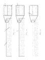
- Figures 1a to 1f illustrate the process steps for direct bonding of blanket wafers in a wafer to wafer bonding process according to the invention.
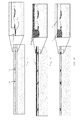
- Figures 2a to 2h illustrate the process steps for direct bonding of hybrid wafers in a wafer to wafer bonding process according to the invention.
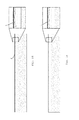
- Figures 3 and 4 illustrate the high bond strength obtainable by the method of the invention on the basis of a number of comparative experimental results.
- silicon oxide and silicon carbon nitride are defined as follows.
- Silicon oxide is defined by the formula SiO x , with x between 1.4 and 2.1.
- Silicon carbon nitride, hereafter referred to as SiCN is defined by the formula SiC y N z with y between 0.7 and 1.1 and z between 0.1 and 0.4.
- the term SiCN also includes layers of SiC y N z :H, wherein the 'H' represents hydrogen atoms attached to the SiCN molecules. This may be obtained as a consequence of the precursors used in the deposition method for the SiCN layers.
- Figure 1 illustrates the process steps of a wafer-to-wafer bonding process according to the invention, for the direct bonding of two blanket wafers, i.e. wafers covered over their entire surface with a dielectric bonding layer.
- the wafers may be silicon wafers comprising a silicon bulk portion 1 and a functional layer 2 which may comprise semiconductor devices together with a stack of interconnect layers, said functional layer being best known in the art as a FEOL/BEOL layer (Front-end-of-line/Back-end-of-line).
- the aim is to produce a bond between two such wafers.
- a microscopic but significant roughness is exhibited by the FEOL/BEOL layer 2, which may be mainly due to a degree of surface topography of the layer.
- a thick layer 3 of SiO x is then deposited onto the FEOL/BEOL layer 2, see Figure 1b , covering the totality of said FEOL/BEOL layer 2.
- the SiO x layer thickness is high compared to the roughness of the FEOL/BEOL layer, e.g. at least ten times higher that said roughness (expressed as RMS value or expressed as a step height value when the roughness of the FEOL/BEOL layer 2 is mainly defined by the topography).
- the SiO x layer 3 may have a thickness between 100 nm and 6 micron.
- the SiO x layer is then thinned by a CMP step, thereby reducing the roughness to a lower value, preferably lower than 0.2 nm RMS ( Figure 1c ).
- a SiO x layer other dielectric layers may be used, e.g. a silicon nitride layer.
- the dielectric layer 3 is an inorganic dielectric layer. An organic dielectric layer 3 is not excluded, but in that case, a curing step of the dielectric layer is required to avoid outgassing of the layer during subsequent process steps.
- a layer 4 of SiCN is deposited onto the thinned SiO x layer ( Figure 1d ).
- the deposition may take place by Plasma Enhanced Chemical Vapour Deposition (PECVD), resulting in an amorphous SiCN layer 4.
- the SiCN layer is thin, preferably between 10 nm and 1 micron, more preferably between 50 nm and 150 nm.
- the wafers are then subjected to an pre-bond annealing step.
- a CMP step is then performed on the SiCN layer, reducing the roughness of the layer to the order of tenths of a nanometre, preferably having a roughness of less than 0.1nm RMS ( Figure 1e ).
- the steps illustrated in Figures 1a to 1d may be performed as part of a BEOL integration scheme.
- the pre-bond anneal temperature is preferably compatible with such an integration scheme, and may be between 400°C and 450°C, preferably around 420°C.
- the wafers which have both been prepared in the above-described way are then aligned and bonded ( Figure 1f ) to form an assembly of the two bonded substrates.
- Any standard alignment technique known in the art can be used, for example based on a camera image of the wafers to be aligned or based on interferometry.
- a number of pre-treatments are performed on the contact surfaces, such as a plasma treatment and/or a cleaning step (e.g. megasonic cleaning).
- the bonding takes place in a bonding tool as known per se in the art, wherein possibly some of the pre-treatments may be performed as well.
- the bond is produced by bringing the two polished SiCN surfaces in contact with each other under appropriate process conditions (see further).
- the extremely low surface roughness facilitates the formation of chemical bonds between the contact surfaces, thereby improving the bond strength between the wafers.
- the bond strength is further improved by a post-bond annealing step performed while the wafers are in contact, at a temperature of less than or equal to 250°C, preferably between 200°C and 250°C. Despite the low anneal temperature, the bond strength between the wafers is excellent.
- FIG. 2 illustrates the method of the invention in the case of the direct bonding of hybrid dielectric/metal wafers.
- Each of the wafers that are to be bonded comprises metal islands 10 on the surface of the FEOL/BEOL layer 2. These islands can represent contact pads or metal lines.
- the surface of the FEOL/BEOL layer 2 again shows a degree of roughness, as illustrated in the detail of Figure 2a .
- openings 11 in the stack of SiO x /SiCN layers ( Figure 2e ), said openings being formed above a number of the metal islands 10 of the FEOL/BEOL layer 2.
- the formation of these openings can take place by standard lithography steps known in the art and not described in detail here.
- the openings are formed by removing the SiO x and SiCN throughout the complete thickness of the SiO x /SiCN stack, thereby exposing the metal 10 at the bottom of the openings.
- a layer 12 of Cu is deposited in the openings and on top of the wafer. This may be done by any suitable technique known in the art. For example, a barrier layer and a Cu seed layer is deposited
- the steps illustrated in Figures 2a to 2g may be performed as part of a BEOL integration scheme.
- the pre-bond anneal temperature is preferably compatible with such an integration scheme, and may be between 400°C and 450°C, preferably around 420°C.
- the bonding process is illustrated in Figure 2h . Possibly after performing pre-treatments of the type described in relation to Figure 1 , corresponding metal areas are aligned and the bond is established by bringing the wafers in contact with each other under appropriate process conditions (see further). Bond formation between Cu areas preferably requires exerting a mechanical pressure that pushes the wafers together.
- the bonding is followed by a post-bond anneal, at a temperature less than or equal to 250°C, preferably between 200°C and 250°C, resulting again in excellent bond strength between bonded SiCN areas, despite the lower temperatures.
- a post-bond anneal at a temperature less than or equal to 250°C, preferably between 200°C and 250°C, resulting again in excellent bond strength between bonded SiCN areas, despite the lower temperatures.
- the invention includes the method as described above, wherein one of the substrates is a semiconductor die instead of a wafer.
- the process parameters during the bonding process may be chosen according to known bonding technology, in terms of temperature and ambient pressure in the bonding tool, as well as the pressure exerted mechanically to push the substrates against each other. Bonding may take place at room temperature or any other suitable temperature, preferably not higher than 500°C. According to a preferred embodiment, the temperature during bonding is the same or in the same range as the post-bond anneal, so that the post-bond anneal can take place in the same tool without losing time. A preferred range for the temperature during bonding is therefore the same range of 200-250°C identified above for the post-bond anneal.
- the bonding preferably takes place at a low ambient pressure, preferably not lower than 10E-7mBar, more preferably around 10E-6mBar.
- the mechanical force used to push the substrates together may be up to 90kN, with a preferred range between 40-60kN. However in the case of the bonding between blanket wafers (as illustrated in Figure 1 , no metal areas on the surface), the bond may be established without a mechanical force being exerted.
- Two wafers having FEOL/BEOL layers 2 are to be bonded by the method of the invention. They have a surface topology defined by a step height between 20nm and 30nm.
- the deposition of the SiO x layer 3 can take place by PECVD, at 340°C, under a pressure of 1 Torr, using as precursors silane and oxygen-containing gases such as NO, NO 2 or O 2 .
- the CMP on the SiO x layers includes a timed dielectric CMP step and a regular post CMP clean (megasonic cleaning), followed by treatment in 2 brush modules and a vapour dryer, e.g. in an integrated Desica cleaner.
- the SiCN deposition takes place by PECVD, at 340°C and 1 Torr.
- the precursor gases include a mixture of at least two types of gases :
- the pre-bond anneal takes place at 420°C during 20 min, in a dissociated ammonia atmosphere containing 10%H 2 .
- the CMP on the SiCN layer includes a timed dielectric CMP step and a regular post CMP clean (megasonic cleaning), followed by treatment in 2 brush modules and a vapour dryer, e.g. in an integrated Desica cleaner, followed by a BTA (benzotriazole) rinse step.
- the post bonding annealing step is performed at 250°C during 120 min in a dissociated ammonia atmosphere comprising 10% H 2 .
- Figure 3 illustrates the bond strength (expressed as the bonding energy in J/cm 2 ) obtained between SiCN layers produced with the above-described method, and compared to the bond strength obtained with other bonding layers, subjected to the same bonding process, including a post-bond annealing step at 250°C during 2hours.
- the layers to which the invention is compared were plasma enhanced silicon oxide (PE ox) and SiN. It is clear that the bond strength between SiCN layers obtained by the method of the invention is superior to the other materials.
- Figure 4 shows bond strengths obtained between PE-ox layers as a function of the post-bond anneal temperature (each time annealing took place during 2hours). Even at a temperature of 450°C, the bond strength is lower than the bond strength obtained between SiCN layers annealed at 250°C, according to the method of the invention.
- the description of a layer being present, deposited or produced 'on' another layer or substrate includes the options of
Landscapes
- Internal Circuitry In Semiconductor Integrated Circuit Devices (AREA)
- Engineering & Computer Science (AREA)
- Manufacturing & Machinery (AREA)
Abstract
Description
- The present invention is related to direct bonding processes wherein a semiconductor substrate is bonded to another semiconductor substrate by forming chemical bonds between the contact surfaces.
- Direct bonding on wafer level, commonly referred to as 'wafer to wafer' bonding, involves the alignment and contacting at room temperature of two semiconductor wafers, usually silicon wafers, followed by an annealing step, during which step chemical bonds are formed between the materials on at least a portion of the contacted wafer surfaces.
- Current wafer to wafer bonding practice falls in two main categories:
- ∘ The surface of both wafers are blanket, flat unpatterned dielectric bonding layers, such as silicon oxide, silicon nitride or a silicon-carbon-oxide (low-k dielectric) layer.
- ∘ The surface of both wafers are flat, patterned dielectric/metal layers (so called hybrid wafer bonding). The main area fraction is covered by the dielectric material, while other areas are metallic, mainly forming contact pads and metal lines. Bonding between dielectric areas takes place by the same mechanism as described above. Locations where metallic areas overlap can be used to realize electrical contacts between the wafers.
- For both categories, the challenge is to achieve a very flat, low roughness dielectric bonding layer which is beneficial for obtaining void-free bonds with a high bond strength. Chemical Mechanical Polishing (CMP) is applied to reduce the roughness of the dielectric layers. Surface treatments are applied such as plasma treatment and ultrasonic or other cleaning techniques. Required post-bond annealing temperatures are generally higher than 400°C in order to reach the desired bond strength. In order to reduce the thermal budget of the bonding process, it is desirable to obtain high strength bonds at lower temperatures. This is particularly important in the field of memory devices.
- For the second category, an additional problem is the diffusion of the metal into the dielectric bonding layer. This is the case for example when silicon oxide bonding is applied to bonding of hybrid wafers that comprise copper line patterns, resulting in direct Cu contact to the oxide surface of the mating wafer. During annealing, the Cu may diffuse in the oxide, resulting in leakage or shorting between interconnect nets. In order to avoid this diffusion, a dielectric bonding layer can be applied that forms a barrier against the Cu-diffusion, such as silicon nitride. However, this makes achieving a high bonding force more difficult and increases the interconnect capacitance due to the higher dielectric constant of the Si nitride versus the Si oxide.
- The same problems are confronted in the 'die to wafer' bonding processes, wherein a silicon chip is bonded to a carrier wafer by direct bonding. In the latter domain, it has been known to apply Silicon Carbon Nitride (SiCN) as the dielectric bonding layer. Reference is made to
US2013/0207268 . Like silicon nitride, SiCN is a good Cu diffusion barrier. However, the cited document fails to describe the bonding process in detail and no information is given on applicable annealing temperatures.US2010/0211849 describes SiCN as a 'bonding aid film' in a direct wafer to wafer bonding process. This process is however open to further improvement in terms of the thermal budget (the post-bonding annealing temperature is 400°C). - The invention is related to a method as disclosed in the appended claims. The present invention is related to a method for bonding a first semiconductor substrate to a second semiconductor substrate by direct bonding, wherein the substrates are both provided on their contact surfaces with a dielectric layer, followed by a CMP step for reducing the roughness of the dielectric layer. Preferably, the dielectric layer after CMP has an roughness of less than 0.2nm RMS. Then a layer of SiCN is deposited onto the thinned dielectric layer, followed by a CMP step which reduces the roughness of the SiCN layer to the order of 1 tenth of a nanometre. Preferably the RMS value after CMP is less than 0.1nm RMS. Then the substrates are subjected to a pre-bond annealing step. The substrates are then bonded by direct bonding, possibly preceded by one or more pre-treatments of the contact surfaces, and followed by a post-bond annealing step, at a temperature of less than or equal to 250°C, preferably between 200°C and 250°C. It has been found that the bond strength is excellent, even at the above named annealing temperatures, which are lower than presently known in the art.
- The invention is thus related to a method for bonding a first semiconductor substrate to a second semiconductor substrate, wherein both substrates are subjected to the following steps, prior to bonding :
- deposition of a dielectric layer on the surface of the substrate,
- subjecting the dielectric layer to a CMP step to reduce the roughness of said dielectric layer,
- deposition of a silicon carbon nitride layer on the surface of the dielectric layer,
- subjecting the substrate to a pre-bond annealing step,
- subjecting the SiCN layer to a CMP step to reduce the
roughness of said SiCN layer, - aligning the substrates,
- bringing the SiCN layers of both substrates into physical contact, to form an assembly of bonded substrates,
- According to a preferred embodiment, the annealing temperature of the post-bond annealing step is less than or equal to 250°C, more preferably said temperature is between 200°C and 250°C.
- According to an embodiment, the roughness of the SiCN layer on both substrates, after the step of subjecting the SiCN layers to CMP, is less than or equal to 0.1nm RMS.
- According to an embodiment, the roughness of the dielectric layer on both substrates, after the step of subjecting the dielectric layers to CMP, is less than or equal to 0.2nm. The dielectric layer deposited on the substrates may be a layer of silicon oxide.
- According to one embodiment of the method of the invention, the substrates are blanket wafers, wherein the dielectric and SiCN layers are continuous layers.
- According to another embodiment, the substrates are hybrid dielectric/metal wafers comprising a patterned surface having areas of dielectric material and areas of metal, and the pre-bond annealing step is followed by :
- etching openings in the stack of layers formed by the dielectric layer and the SiCN layer, thereby exposing portions of the metal areas on the substrate,
- depositing metal in said openings and on the surface of the dielectric/SiCN stack,
- wherein the CMP step performed on the SiCN layer is a CMP that starts on the metal layer deposited on the surface of the dielectric/SiCN stack, removing the metal from said surface, and stopping on the SiCN layer, thereby reducing the roughness of said SiCN layer.
- According to an embodiment, the temperature during bonding is the same as the post-bond annealing temperature. The pre-bond annealing temperature may be between 400°C and 450°C.
-
Figures 1a to 1f illustrate the process steps for direct bonding of blanket wafers in a wafer to wafer bonding process according to the invention. -
Figures 2a to 2h illustrate the process steps for direct bonding of hybrid wafers in a wafer to wafer bonding process according to the invention. -
Figures 3 and 4 illustrate the high bond strength obtainable by the method of the invention on the basis of a number of comparative experimental results. - In the following description, the materials silicon oxide and silicon carbon nitride are defined as follows. Silicon oxide is defined by the formula SiOx, with x between 1.4 and 2.1. Silicon carbon nitride, hereafter referred to as SiCN, is defined by the formula SiCyNz with y between 0.7 and 1.1 and z between 0.1 and 0.4. The term SiCN also includes layers of SiCyNz:H, wherein the 'H' represents hydrogen atoms attached to the SiCN molecules. This may be obtained as a consequence of the precursors used in the deposition method for the SiCN layers.
-
Figure 1 illustrates the process steps of a wafer-to-wafer bonding process according to the invention, for the direct bonding of two blanket wafers, i.e. wafers covered over their entire surface with a dielectric bonding layer. As illustrated inFigure 1a , the wafers may be silicon wafers comprising asilicon bulk portion 1 and afunctional layer 2 which may comprise semiconductor devices together with a stack of interconnect layers, said functional layer being best known in the art as a FEOL/BEOL layer (Front-end-of-line/Back-end-of-line). The aim is to produce a bond between two such wafers. As seen in the detail ofFigure 1a , a microscopic but significant roughness is exhibited by the FEOL/BEOL layer 2, which may be mainly due to a degree of surface topography of the layer. - A
thick layer 3 of SiOx is then deposited onto the FEOL/BEOL layer 2, seeFigure 1b , covering the totality of said FEOL/BEOL layer 2. As illustrated in the detail ofFigure 1b , the SiOx layer thickness is high compared to the roughness of the FEOL/BEOL layer, e.g. at least ten times higher that said roughness (expressed as RMS value or expressed as a step height value when the roughness of the FEOL/BEOL layer 2 is mainly defined by the topography). In absolute terms, the SiOx layer 3 may have a thickness between 100 nm and 6 micron. The SiOx layer is then thinned by a CMP step, thereby reducing the roughness to a lower value, preferably lower than 0.2 nm RMS (Figure 1c ). Instead of a SiOx layer, other dielectric layers may be used, e.g. a silicon nitride layer. Preferably, thedielectric layer 3 is an inorganic dielectric layer. Anorganic dielectric layer 3 is not excluded, but in that case, a curing step of the dielectric layer is required to avoid outgassing of the layer during subsequent process steps. - Then a
layer 4 of SiCN is deposited onto the thinned SiOx layer (Figure 1d ). The deposition may take place by Plasma Enhanced Chemical Vapour Deposition (PECVD), resulting in anamorphous SiCN layer 4. The SiCN layer is thin, preferably between 10 nm and 1 micron, more preferably between 50 nm and 150 nm. The wafers are then subjected to an pre-bond annealing step. - A CMP step is then performed on the SiCN layer, reducing the roughness of the layer to the order of tenths of a nanometre, preferably having a roughness of less than 0.1nm RMS (
Figure 1e ). The steps illustrated inFigures 1a to 1d may be performed as part of a BEOL integration scheme. In that case, the pre-bond anneal temperature is preferably compatible with such an integration scheme, and may be between 400°C and 450°C, preferably around 420°C. - The wafers which have both been prepared in the above-described way, are then aligned and bonded (
Figure 1f ) to form an assembly of the two bonded substrates. Any standard alignment technique known in the art can be used, for example based on a camera image of the wafers to be aligned or based on interferometry. Possibly a number of pre-treatments are performed on the contact surfaces, such as a plasma treatment and/or a cleaning step (e.g. megasonic cleaning). The bonding takes place in a bonding tool as known per se in the art, wherein possibly some of the pre-treatments may be performed as well. - The bond is produced by bringing the two polished SiCN surfaces in contact with each other under appropriate process conditions (see further). The extremely low surface roughness facilitates the formation of chemical bonds between the contact surfaces, thereby improving the bond strength between the wafers.
- The bond strength is further improved by a post-bond annealing step performed while the wafers are in contact, at a temperature of less than or equal to 250°C, preferably between 200°C and 250°C. Despite the low anneal temperature, the bond strength between the wafers is excellent.
-
Figure 2 illustrates the method of the invention in the case of the direct bonding of hybrid dielectric/metal wafers. Each of the wafers that are to be bonded comprisesmetal islands 10 on the surface of the FEOL/BEOL layer 2. These islands can represent contact pads or metal lines. The surface of the FEOL/BEOL layer 2 again shows a degree of roughness, as illustrated in the detail ofFigure 2a . InFigures 2b, 2c and 2d , the same steps are performed as described in the case of the blanket wafers : deposition of a thicksilicon oxide layer 3 and CMP on said layer, thinning the SiOx layer by CMP (preferably to a roughness of less than 0.2 nm RMS), and deposition of aSiCN layer 4 on the thinned SiOx layer. A pre-bond annealing step is again performed at this point. - This is now followed by the production of
openings 11 in the stack of SiOx/SiCN layers (Figure 2e ), said openings being formed above a number of themetal islands 10 of the FEOL/BEOL layer 2. The formation of these openings can take place by standard lithography steps known in the art and not described in detail here. The openings are formed by removing the SiOx and SiCN throughout the complete thickness of the SiOx/SiCN stack, thereby exposing themetal 10 at the bottom of the openings. Then alayer 12 of Cu is deposited in the openings and on top of the wafer. This may be done by any suitable technique known in the art. For example, a barrier layer and a Cu seed layer is deposited - (not shown), followed by the electrodeposition of
Cu 12 inside the openings and on top of the wafer (Figure 2f ). A CMP step is then performed which removes the Cu from the upper surface of the wafer. TheSiCN layer 4 acts as a stopping layer for the CMP, as it exhibits a higher resistance to CMP than copper. At the same time, the CMP step reduces the roughness of the SiCN layer to the order of tenths of a nanometre, preferably less than 0.1nm RMS. This results in the wafer as shown inFigure 2g , whereCu regions 13 are surrounded bysmooth SiCN areas 14. Once again, the steps illustrated inFigures 2a to 2g may be performed as part of a BEOL integration scheme. In that case, the pre-bond anneal temperature is preferably compatible with such an integration scheme, and may be between 400°C and 450°C, preferably around 420°C. - The bonding process is illustrated in
Figure 2h . Possibly after performing pre-treatments of the type described in relation toFigure 1 , corresponding metal areas are aligned and the bond is established by bringing the wafers in contact with each other under appropriate process conditions (see further). Bond formation between Cu areas preferably requires exerting a mechanical pressure that pushes the wafers together. - The bonding is followed by a post-bond anneal, at a temperature less than or equal to 250°C, preferably between 200°C and 250°C, resulting again in excellent bond strength between bonded SiCN areas, despite the lower temperatures. The added advantage of using SiCN in this case is that the SiCN forms a barrier against Cu-diffusion.
- The invention includes the method as described above, wherein one of the substrates is a semiconductor die instead of a wafer.
- In any of the above-described embodiments, the process parameters during the bonding process, i.e. after pre-bond annealing and before post-bond annealing, may be chosen according to known bonding technology, in terms of temperature and ambient pressure in the bonding tool, as well as the pressure exerted mechanically to push the substrates against each other. Bonding may take place at room temperature or any other suitable temperature, preferably not higher than 500°C. According to a preferred embodiment, the temperature during bonding is the same or in the same range as the post-bond anneal, so that the post-bond anneal can take place in the same tool without losing time. A preferred range for the temperature during bonding is therefore the same range of 200-250°C identified above for the post-bond anneal. The bonding preferably takes place at a low ambient pressure, preferably not lower than 10E-7mBar, more preferably around 10E-6mBar. The mechanical force used to push the substrates together may be up to 90kN, with a preferred range between 40-60kN. However in the case of the bonding between blanket wafers (as illustrated in
Figure 1 , no metal areas on the surface), the bond may be established without a mechanical force being exerted. - In the following, a number of preferred process parameters are described for performing the method of the invention. The values given hereafter are given purely by way of example and are not limiting the scope of the present invention.
- Two wafers having FEOL/
BEOL layers 2 are to be bonded by the method of the invention. They have a surface topology defined by a step height between 20nm and 30nm. The deposition of the SiOx layer 3 can take place by PECVD, at 340°C, under a pressure of 1 Torr, using as precursors silane and oxygen-containing gases such as NO, NO2 or O2. - A preferred value of the SiOx thickness is around 900nm. The CMP on the SiOx layers includes a timed dielectric CMP step and a regular post CMP clean (megasonic cleaning), followed by treatment in 2 brush modules and a vapour dryer, e.g. in an integrated Desica cleaner.
- The SiCN deposition takes place by PECVD, at 340°C and 1 Torr. The precursor gases include a mixture of at least two types of gases :
- 1) Si-C containing gases such as Tri-methyl silane and tetra-methyl-silane
- 2) N containing gases such as NH3, normally diluted in N2
- The pre-bond anneal takes place at 420°C during 20 min, in a dissociated ammonia atmosphere containing 10%H2.
- The CMP on the SiCN layer includes a timed dielectric CMP step and a regular post CMP clean (megasonic cleaning), followed by treatment in 2 brush modules and a vapour dryer, e.g. in an integrated Desica cleaner, followed by a BTA (benzotriazole) rinse step. The post bonding annealing step is performed at 250°C during 120 min in a dissociated ammonia atmosphere comprising 10% H2.
-
Figure 3 illustrates the bond strength (expressed as the bonding energy in J/cm2) obtained between SiCN layers produced with the above-described method, and compared to the bond strength obtained with other bonding layers, subjected to the same bonding process, including a post-bond annealing step at 250°C during 2hours. The layers to which the invention is compared were plasma enhanced silicon oxide (PE ox) and SiN. It is clear that the bond strength between SiCN layers obtained by the method of the invention is superior to the other materials. -
Figure 4 shows bond strengths obtained between PE-ox layers as a function of the post-bond anneal temperature (each time annealing took place during 2hours). Even at a temperature of 450°C, the bond strength is lower than the bond strength obtained between SiCN layers annealed at 250°C, according to the method of the invention. - While the invention has been illustrated and described in detail in the drawings and foregoing description, such illustration and description are to be considered illustrative or exemplary and not restrictive. Other variations to the disclosed embodiments can be understood and effected by those skilled in the art in practicing the claimed invention, from a study of the drawings, the disclosure and the appended claims. In the claims, the word "comprising" does not exclude other elements or steps, and the indefinite article "a" or "an" does not exclude a plurality. The mere fact that certain measures are recited in mutually different dependent claims does not indicate that a combination of these measures cannot be used to advantage. Any reference signs in the claims should not be construed as limiting the scope.
- Unless specifically specified, the description of a layer being present, deposited or produced 'on' another layer or substrate, includes the options of
- said layer being present, produced or deposited directly on, i.e. in physical contact with, said other layer or substrate, and
- said layer being present, produced or deposited on one or a stack of intermediate layers between said layer and said other layer or substrate.
Claims (10)
- A method for bonding a first semiconductor substrate to a second semiconductor substrate, wherein both substrates are subjected to the following steps, prior to bonding :• deposition of a dielectric layer (3) on the surface of the substrate,• subjecting the dielectric layer (3) to a CMP step to reduce the roughness of said dielectric layer,• deposition of a silicon carbon nitride layer (4) on the surface of the dielectric layer,• subjecting the substrate to a pre-bond annealing step,• subjecting the SiCN layer (4) to a CMP step to reduce the roughness of said SiCN layer,wherein the bonding comprises :• aligning the substrates,• bringing the SiCN layers (4) of both substrates into physical contact, to form an assembly of bonded substrates,and wherein the method further comprises the step of subjecting the assembly to a post-bond annealing step.
- Method according to claim 1, wherein the annealing temperature of the post-bond annealing step is less than or equal to 250°C.
- Method according to claim 2, wherein said temperature is between 200°C and 250°C.
- Method according to any one of claims 1 to 3, wherein the roughness of the SiCN layer (4) on both substrates, after the step of subjecting the SiCN layers to CMP, is less than or equal to 0.1nm RMS.
- Method according to any one of the preceding claims, wherein the roughness of the dielectric layer (3) on both substrates, after the step of subjecting the dielectric layers to CMP, is less than or equal to 0.2nm.
- Method according to any one of the preceding claims, wherein the dielectric layer (3) deposited on the substrates is a layer of silicon oxide.
- Method according to any one of the preceding claims, wherein the substrates are blanket wafers and wherein the dielectric and SiCN layers (3,4) are continuous layers.
- Method according to any one of claims 1 to 6, wherein the substrates are hybrid dielectric/metal wafers comprising a patterned surface having areas of dielectric material and areas (10) of metal, and wherein the pre-bond annealing step is followed by :• etching openings (11) in the stack of layers formed by the dielectric layer (3) and the SiCN layer (4), thereby exposing portions of the metal areas (10) on the substrate,• depositing metal (12) in said openings (11) and on the surface of the dielectric/SiCN stack,• and wherein the CMP step performed on the SiCN layer (4) is a CMP that starts on the metal layer (12) deposited on the surface of the dielectric/SiCN stack, removing the metal from said surface, and stopping on the SiCN layer (4), thereby reducing the roughness of said SiCN layer.
- Method according to any one of the preceding claims, wherein the temperature during bonding is the same as the post-bond annealing temperature.
- Method according to any one of the preceding claims, wherein the pre-bond annealing temperature is between 400°C and 450°C.
Priority Applications (3)
| Application Number | Priority Date | Filing Date | Title |
|---|---|---|---|
| EP14194506.3A EP3024019B1 (en) | 2014-11-24 | 2014-11-24 | Method for direct bonding of semiconductor substrates. |
| PCT/EP2015/077424 WO2016083332A1 (en) | 2014-11-24 | 2015-11-24 | Method for direct bonding of semiconductor substrates |
| US15/604,454 US10141284B2 (en) | 2014-11-24 | 2017-05-24 | Method of bonding semiconductor substrates |
Applications Claiming Priority (1)
| Application Number | Priority Date | Filing Date | Title |
|---|---|---|---|
| EP14194506.3A EP3024019B1 (en) | 2014-11-24 | 2014-11-24 | Method for direct bonding of semiconductor substrates. |
Publications (2)
| Publication Number | Publication Date |
|---|---|
| EP3024019A1 true EP3024019A1 (en) | 2016-05-25 |
| EP3024019B1 EP3024019B1 (en) | 2025-02-26 |
Family
ID=51982439
Family Applications (1)
| Application Number | Title | Priority Date | Filing Date |
|---|---|---|---|
| EP14194506.3A Active EP3024019B1 (en) | 2014-11-24 | 2014-11-24 | Method for direct bonding of semiconductor substrates. |
Country Status (3)
| Country | Link |
|---|---|
| US (1) | US10141284B2 (en) |
| EP (1) | EP3024019B1 (en) |
| WO (1) | WO2016083332A1 (en) |
Cited By (2)
| Publication number | Priority date | Publication date | Assignee | Title |
|---|---|---|---|---|
| EP3376524A1 (en) * | 2017-02-28 | 2018-09-19 | Imec Vzw | A method for direct bonding of semiconductor substrates |
| WO2025201786A1 (en) * | 2024-03-27 | 2025-10-02 | Asml Netherlands B.V. | Method for bonding semiconductor substrates |
Families Citing this family (11)
| Publication number | Priority date | Publication date | Assignee | Title |
|---|---|---|---|---|
| EP3024019B1 (en) | 2014-11-24 | 2025-02-26 | IMEC vzw | Method for direct bonding of semiconductor substrates. |
| US10658313B2 (en) | 2017-12-11 | 2020-05-19 | Invensas Bonding Technologies, Inc. | Selective recess |
| WO2020000380A1 (en) * | 2018-06-29 | 2020-01-02 | 长江存储科技有限责任公司 | Semiconductor structure and forming method therefor |
| EP3667745B1 (en) | 2018-12-10 | 2023-03-22 | IMEC vzw | Method for obtaining light emitting diodes reconstituted over a carrier substrate |
| JP7421292B2 (en) * | 2019-09-11 | 2024-01-24 | キオクシア株式会社 | Manufacturing method of semiconductor device |
| CN114467164A (en) * | 2019-09-12 | 2022-05-10 | 应用材料公司 | Repellent web and deposition method |
| US20220119952A1 (en) * | 2020-10-20 | 2022-04-21 | Applied Materials, Inc. | Method of reducing defects in a multi-layer pecvd teos oxide film |
| US12147083B2 (en) * | 2020-12-16 | 2024-11-19 | Intel Corporation | Hybrid manufacturing for integrating photonic and electronic components |
| US12176321B2 (en) * | 2021-03-31 | 2024-12-24 | Taiwan Semiconductor Manufacturing Company, Ltd. | Semiconductor packages and method of forming the same |
| CN115346915B (en) * | 2021-05-14 | 2026-08-07 | 联华电子股份有限公司 | Semiconductor device manufacturing methods |
| CN115890021B (en) * | 2023-01-05 | 2023-05-16 | 成都功成半导体有限公司 | Wafer laser cutting method and wafer |
Citations (5)
| Publication number | Priority date | Publication date | Assignee | Title |
|---|---|---|---|---|
| US20100211849A1 (en) | 2009-02-19 | 2010-08-19 | Nec Laboratories America, Inc. | Multi-dimensional ldpc coded modulation for high-speed optical transmission systems |
| US20130009321A1 (en) * | 2011-07-05 | 2013-01-10 | Sony Corporation | Semiconductor device, fabrication method for a semiconductor device and electronic apparatus |
| FR2978606A1 (en) * | 2011-07-27 | 2013-02-01 | Soitec Silicon On Insulator | Method for direct bonding of microelectronic components, involves defining semiconductor bonding planes for semiconductor structures, respectively, and sticking device structures by directly bonding conducting materials |
| US20130207268A1 (en) | 2012-02-14 | 2013-08-15 | Stmicroelectronics (Crolles 2) Sas | Chip assembly system |
| US20130270328A1 (en) * | 2010-07-21 | 2013-10-17 | Commissariat A L'energie Atomique Et Aux Ene Alt | Process for direct bonding two elements comprising copper portions and portions of dielectric materials |
Family Cites Families (7)
| Publication number | Priority date | Publication date | Assignee | Title |
|---|---|---|---|---|
| US6984571B1 (en) * | 1999-10-01 | 2006-01-10 | Ziptronix, Inc. | Three dimensional device integration method and integrated device |
| US8993460B2 (en) * | 2013-01-10 | 2015-03-31 | Novellus Systems, Inc. | Apparatuses and methods for depositing SiC/SiCN films via cross-metathesis reactions with organometallic co-reactants |
| FR2963982B1 (en) * | 2010-08-20 | 2012-09-28 | Soitec Silicon On Insulator | LOW TEMPERATURE BONDING PROCESS |
| JP2012174937A (en) * | 2011-02-22 | 2012-09-10 | Sony Corp | Semiconductor device, manufacturing method of semiconductor device, bonding method of semiconductor wafer and electronic apparatus |
| JP5853389B2 (en) * | 2011-03-28 | 2016-02-09 | ソニー株式会社 | Semiconductor device and manufacturing method of semiconductor device. |
| US9284472B2 (en) * | 2013-08-09 | 2016-03-15 | Fujimi Incorporated | SiCN and SiN polishing slurries and polishing methods using the same |
| EP3024019B1 (en) | 2014-11-24 | 2025-02-26 | IMEC vzw | Method for direct bonding of semiconductor substrates. |
-
2014
- 2014-11-24 EP EP14194506.3A patent/EP3024019B1/en active Active
-
2015
- 2015-11-24 WO PCT/EP2015/077424 patent/WO2016083332A1/en not_active Ceased
-
2017
- 2017-05-24 US US15/604,454 patent/US10141284B2/en active Active
Patent Citations (5)
| Publication number | Priority date | Publication date | Assignee | Title |
|---|---|---|---|---|
| US20100211849A1 (en) | 2009-02-19 | 2010-08-19 | Nec Laboratories America, Inc. | Multi-dimensional ldpc coded modulation for high-speed optical transmission systems |
| US20130270328A1 (en) * | 2010-07-21 | 2013-10-17 | Commissariat A L'energie Atomique Et Aux Ene Alt | Process for direct bonding two elements comprising copper portions and portions of dielectric materials |
| US20130009321A1 (en) * | 2011-07-05 | 2013-01-10 | Sony Corporation | Semiconductor device, fabrication method for a semiconductor device and electronic apparatus |
| FR2978606A1 (en) * | 2011-07-27 | 2013-02-01 | Soitec Silicon On Insulator | Method for direct bonding of microelectronic components, involves defining semiconductor bonding planes for semiconductor structures, respectively, and sticking device structures by directly bonding conducting materials |
| US20130207268A1 (en) | 2012-02-14 | 2013-08-15 | Stmicroelectronics (Crolles 2) Sas | Chip assembly system |
Cited By (2)
| Publication number | Priority date | Publication date | Assignee | Title |
|---|---|---|---|---|
| EP3376524A1 (en) * | 2017-02-28 | 2018-09-19 | Imec Vzw | A method for direct bonding of semiconductor substrates |
| WO2025201786A1 (en) * | 2024-03-27 | 2025-10-02 | Asml Netherlands B.V. | Method for bonding semiconductor substrates |
Also Published As
| Publication number | Publication date |
|---|---|
| US20170301646A1 (en) | 2017-10-19 |
| WO2016083332A1 (en) | 2016-06-02 |
| EP3024019B1 (en) | 2025-02-26 |
| US10141284B2 (en) | 2018-11-27 |
Similar Documents
| Publication | Publication Date | Title |
|---|---|---|
| EP3024019B1 (en) | Method for direct bonding of semiconductor substrates. | |
| JP6014354B2 (en) | Manufacturing method of semiconductor device | |
| CN100468639C (en) | Room temperature covalent bonding method | |
| KR100574731B1 (en) | Manufacturing method of semiconductor device | |
| JP2025542482A (en) | Direct bonded metal structure with aluminum features and method of making same | |
| US9716076B2 (en) | Method for manufacturing semiconductor device with metal-containing film layer at bonding surface thereof | |
| KR101252292B1 (en) | Room temperature metal direct bonding | |
| US20070281439A1 (en) | Techniques for Layer Transfer Processing | |
| US7371662B2 (en) | Method for forming a 3D interconnect and resulting structures | |
| JPWO2010098151A1 (en) | Semiconductor device and manufacturing method thereof | |
| EP3671812B1 (en) | A method for bonding and interconnecting semiconductor chips | |
| CN105185719A (en) | Lock type hybrid bonding method | |
| US12532780B2 (en) | Hybrid bonding for semiconductor device assemblies | |
| CN103180947B (en) | There is the integrated circuit of zero temperature coefficient capacitor | |
| US6881661B2 (en) | Manufacturing method of semiconductor device | |
| CN115910817A (en) | Wafer bonding method and semiconductor device | |
| JP2008010884A (en) | Manufacturing method of semiconductor device | |
| US20250210553A1 (en) | Semiconductor structure and fabrication method thereof | |
| CN111312689B (en) | Top layer copper process structure of integrated circuit and manufacturing method thereof | |
| TW444343B (en) | Manufacturing method of inter-level dielectrics | |
| JP3774217B2 (en) | Method for forming insulating film and method for manufacturing semiconductor device | |
| TW202329248A (en) | Method for manufacturing semiconductor structure | |
| US20220367182A1 (en) | Method for manufacturing semiconductor device | |
| TW413899B (en) | Manufacturing process of unlanded via | |
| TW515006B (en) | Method for removing moistured part of FSG layer after polishing treatment |
Legal Events
| Date | Code | Title | Description |
|---|---|---|---|
| AK | Designated contracting states |
Kind code of ref document: A1 Designated state(s): AL AT BE BG CH CY CZ DE DK EE ES FI FR GB GR HR HU IE IS IT LI LT LU LV MC MK MT NL NO PL PT RO RS SE SI SK SM TR |
|
| AX | Request for extension of the european patent |
Extension state: BA ME |
|
| PUAI | Public reference made under article 153(3) epc to a published international application that has entered the european phase |
Free format text: ORIGINAL CODE: 0009012 |
|
| STAA | Information on the status of an ep patent application or granted ep patent |
Free format text: STATUS: REQUEST FOR EXAMINATION WAS MADE |
|
| 17P | Request for examination filed |
Effective date: 20161125 |
|
| RBV | Designated contracting states (corrected) |
Designated state(s): AL AT BE BG CH CY CZ DE DK EE ES FI FR GB GR HR HU IE IS IT LI LT LU LV MC MK MT NL NO PL PT RO RS SE SI SK SM TR |
|
| R17P | Request for examination filed (corrected) |
Effective date: 20161125 |
|
| STAA | Information on the status of an ep patent application or granted ep patent |
Free format text: STATUS: EXAMINATION IS IN PROGRESS |
|
| 17Q | First examination report despatched |
Effective date: 20190712 |
|
| RIC1 | Information provided on ipc code assigned before grant |
Ipc: H01L 21/3105 20060101ALN20240906BHEP Ipc: H01L 21/02 20060101ALN20240906BHEP Ipc: H01L 23/31 20060101ALN20240906BHEP Ipc: H01L 21/20 20060101ALI20240906BHEP Ipc: H01L 21/60 20060101AFI20240906BHEP |
|
| GRAP | Despatch of communication of intention to grant a patent |
Free format text: ORIGINAL CODE: EPIDOSNIGR1 |
|
| STAA | Information on the status of an ep patent application or granted ep patent |
Free format text: STATUS: GRANT OF PATENT IS INTENDED |
|
| RIC1 | Information provided on ipc code assigned before grant |
Ipc: H01L 21/3105 20060101ALN20241015BHEP Ipc: H01L 21/02 20060101ALN20241015BHEP Ipc: H01L 23/31 20060101ALN20241015BHEP Ipc: H01L 21/20 20060101ALI20241015BHEP Ipc: H01L 21/60 20060101AFI20241015BHEP |
|
| INTG | Intention to grant announced |
Effective date: 20241023 |
|
| GRAS | Grant fee paid |
Free format text: ORIGINAL CODE: EPIDOSNIGR3 |
|
| GRAA | (expected) grant |
Free format text: ORIGINAL CODE: 0009210 |
|
| STAA | Information on the status of an ep patent application or granted ep patent |
Free format text: STATUS: THE PATENT HAS BEEN GRANTED |
|
| AK | Designated contracting states |
Kind code of ref document: B1 Designated state(s): AL AT BE BG CH CY CZ DE DK EE ES FI FR GB GR HR HU IE IS IT LI LT LU LV MC MK MT NL NO PL PT RO RS SE SI SK SM TR |
|
| REG | Reference to a national code |
Ref country code: GB Ref legal event code: FG4D |
|
| REG | Reference to a national code |
Ref country code: CH Ref legal event code: EP |
|
| REG | Reference to a national code |
Ref country code: DE Ref legal event code: R096 Ref document number: 602014091605 Country of ref document: DE |
|
| REG | Reference to a national code |
Ref country code: IE Ref legal event code: FG4D |
|
| P01 | Opt-out of the competence of the unified patent court (upc) registered |
Free format text: CASE NUMBER: APP_14881/2025 Effective date: 20250327 |
|
| REG | Reference to a national code |
Ref country code: NL Ref legal event code: MP Effective date: 20250226 |
|
| PG25 | Lapsed in a contracting state [announced via postgrant information from national office to epo] |
Ref country code: RS Free format text: LAPSE BECAUSE OF FAILURE TO SUBMIT A TRANSLATION OF THE DESCRIPTION OR TO PAY THE FEE WITHIN THE PRESCRIBED TIME-LIMIT Effective date: 20250526 |
|
| PG25 | Lapsed in a contracting state [announced via postgrant information from national office to epo] |
Ref country code: FI Free format text: LAPSE BECAUSE OF FAILURE TO SUBMIT A TRANSLATION OF THE DESCRIPTION OR TO PAY THE FEE WITHIN THE PRESCRIBED TIME-LIMIT Effective date: 20250226 |
|
| PG25 | Lapsed in a contracting state [announced via postgrant information from national office to epo] |
Ref country code: PL Free format text: LAPSE BECAUSE OF FAILURE TO SUBMIT A TRANSLATION OF THE DESCRIPTION OR TO PAY THE FEE WITHIN THE PRESCRIBED TIME-LIMIT Effective date: 20250226 |
|
| PG25 | Lapsed in a contracting state [announced via postgrant information from national office to epo] |
Ref country code: ES Free format text: LAPSE BECAUSE OF FAILURE TO SUBMIT A TRANSLATION OF THE DESCRIPTION OR TO PAY THE FEE WITHIN THE PRESCRIBED TIME-LIMIT Effective date: 20250226 |
|
| REG | Reference to a national code |
Ref country code: LT Ref legal event code: MG9D |
|
| PG25 | Lapsed in a contracting state [announced via postgrant information from national office to epo] |
Ref country code: IS Free format text: LAPSE BECAUSE OF FAILURE TO SUBMIT A TRANSLATION OF THE DESCRIPTION OR TO PAY THE FEE WITHIN THE PRESCRIBED TIME-LIMIT Effective date: 20250626 Ref country code: NO Free format text: LAPSE BECAUSE OF FAILURE TO SUBMIT A TRANSLATION OF THE DESCRIPTION OR TO PAY THE FEE WITHIN THE PRESCRIBED TIME-LIMIT Effective date: 20250526 |
|
| PG25 | Lapsed in a contracting state [announced via postgrant information from national office to epo] |
Ref country code: NL Free format text: LAPSE BECAUSE OF FAILURE TO SUBMIT A TRANSLATION OF THE DESCRIPTION OR TO PAY THE FEE WITHIN THE PRESCRIBED TIME-LIMIT Effective date: 20250226 |
|
| PG25 | Lapsed in a contracting state [announced via postgrant information from national office to epo] |
Ref country code: HR Free format text: LAPSE BECAUSE OF FAILURE TO SUBMIT A TRANSLATION OF THE DESCRIPTION OR TO PAY THE FEE WITHIN THE PRESCRIBED TIME-LIMIT Effective date: 20250226 |
|
| PG25 | Lapsed in a contracting state [announced via postgrant information from national office to epo] |
Ref country code: LV Free format text: LAPSE BECAUSE OF FAILURE TO SUBMIT A TRANSLATION OF THE DESCRIPTION OR TO PAY THE FEE WITHIN THE PRESCRIBED TIME-LIMIT Effective date: 20250226 Ref country code: PT Free format text: LAPSE BECAUSE OF FAILURE TO SUBMIT A TRANSLATION OF THE DESCRIPTION OR TO PAY THE FEE WITHIN THE PRESCRIBED TIME-LIMIT Effective date: 20250626 |
|
| PG25 | Lapsed in a contracting state [announced via postgrant information from national office to epo] |
Ref country code: GR Free format text: LAPSE BECAUSE OF FAILURE TO SUBMIT A TRANSLATION OF THE DESCRIPTION OR TO PAY THE FEE WITHIN THE PRESCRIBED TIME-LIMIT Effective date: 20250527 Ref country code: BG Free format text: LAPSE BECAUSE OF FAILURE TO SUBMIT A TRANSLATION OF THE DESCRIPTION OR TO PAY THE FEE WITHIN THE PRESCRIBED TIME-LIMIT Effective date: 20250226 |
|
| REG | Reference to a national code |
Ref country code: AT Ref legal event code: MK05 Ref document number: 1771546 Country of ref document: AT Kind code of ref document: T Effective date: 20250226 |
|
| PG25 | Lapsed in a contracting state [announced via postgrant information from national office to epo] |
Ref country code: SE Free format text: LAPSE BECAUSE OF FAILURE TO SUBMIT A TRANSLATION OF THE DESCRIPTION OR TO PAY THE FEE WITHIN THE PRESCRIBED TIME-LIMIT Effective date: 20250226 |
|
| PG25 | Lapsed in a contracting state [announced via postgrant information from national office to epo] |
Ref country code: SM Free format text: LAPSE BECAUSE OF FAILURE TO SUBMIT A TRANSLATION OF THE DESCRIPTION OR TO PAY THE FEE WITHIN THE PRESCRIBED TIME-LIMIT Effective date: 20250226 |
|
| PG25 | Lapsed in a contracting state [announced via postgrant information from national office to epo] |
Ref country code: DK Free format text: LAPSE BECAUSE OF FAILURE TO SUBMIT A TRANSLATION OF THE DESCRIPTION OR TO PAY THE FEE WITHIN THE PRESCRIBED TIME-LIMIT Effective date: 20250226 |
|
| PG25 | Lapsed in a contracting state [announced via postgrant information from national office to epo] |
Ref country code: IT Free format text: LAPSE BECAUSE OF FAILURE TO SUBMIT A TRANSLATION OF THE DESCRIPTION OR TO PAY THE FEE WITHIN THE PRESCRIBED TIME-LIMIT Effective date: 20250226 |
|
| PG25 | Lapsed in a contracting state [announced via postgrant information from national office to epo] |
Ref country code: AT Free format text: LAPSE BECAUSE OF FAILURE TO SUBMIT A TRANSLATION OF THE DESCRIPTION OR TO PAY THE FEE WITHIN THE PRESCRIBED TIME-LIMIT Effective date: 20250226 |
|
| PG25 | Lapsed in a contracting state [announced via postgrant information from national office to epo] |
Ref country code: CZ Free format text: LAPSE BECAUSE OF FAILURE TO SUBMIT A TRANSLATION OF THE DESCRIPTION OR TO PAY THE FEE WITHIN THE PRESCRIBED TIME-LIMIT Effective date: 20250226 Ref country code: EE Free format text: LAPSE BECAUSE OF FAILURE TO SUBMIT A TRANSLATION OF THE DESCRIPTION OR TO PAY THE FEE WITHIN THE PRESCRIBED TIME-LIMIT Effective date: 20250226 |
|
| PG25 | Lapsed in a contracting state [announced via postgrant information from national office to epo] |
Ref country code: RO Free format text: LAPSE BECAUSE OF FAILURE TO SUBMIT A TRANSLATION OF THE DESCRIPTION OR TO PAY THE FEE WITHIN THE PRESCRIBED TIME-LIMIT Effective date: 20250226 |
|
| PG25 | Lapsed in a contracting state [announced via postgrant information from national office to epo] |
Ref country code: SK Free format text: LAPSE BECAUSE OF FAILURE TO SUBMIT A TRANSLATION OF THE DESCRIPTION OR TO PAY THE FEE WITHIN THE PRESCRIBED TIME-LIMIT Effective date: 20250226 |
|
| REG | Reference to a national code |
Ref country code: DE Ref legal event code: R097 Ref document number: 602014091605 Country of ref document: DE |
|
| REG | Reference to a national code |
Ref country code: DE Ref legal event code: R079 Ref document number: 602014091605 Country of ref document: DE Free format text: PREVIOUS MAIN CLASS: H01L0021600000 Ipc: H10W0070010000 |
|
| PLBE | No opposition filed within time limit |
Free format text: ORIGINAL CODE: 0009261 |
|
| STAA | Information on the status of an ep patent application or granted ep patent |
Free format text: STATUS: NO OPPOSITION FILED WITHIN TIME LIMIT |
|
| REG | Reference to a national code |
Ref country code: CH Ref legal event code: L10 Free format text: ST27 STATUS EVENT CODE: U-0-0-L10-L00 (AS PROVIDED BY THE NATIONAL OFFICE) Effective date: 20260107 |
|
| PGFP | Annual fee paid to national office [announced via postgrant information from national office to epo] |
Ref country code: DE Payment date: 20251022 Year of fee payment: 12 |
|
| 26N | No opposition filed |
Effective date: 20251127 |
|
| REG | Reference to a national code |
Ref country code: CH Ref legal event code: H13 Free format text: ST27 STATUS EVENT CODE: U-0-0-H10-H13 (AS PROVIDED BY THE NATIONAL OFFICE) Effective date: 20260623 |
|
| PG25 | Lapsed in a contracting state [announced via postgrant information from national office to epo] |
Ref country code: LT Free format text: LAPSE BECAUSE OF FAILURE TO SUBMIT A TRANSLATION OF THE DESCRIPTION OR TO PAY THE FEE WITHIN THE PRESCRIBED TIME-LIMIT Effective date: 20250226 |
|
| PG25 | Lapsed in a contracting state [announced via postgrant information from national office to epo] |
Ref country code: MC Free format text: LAPSE BECAUSE OF FAILURE TO SUBMIT A TRANSLATION OF THE DESCRIPTION OR TO PAY THE FEE WITHIN THE PRESCRIBED TIME-LIMIT Effective date: 20250226 |
|
| PG25 | Lapsed in a contracting state [announced via postgrant information from national office to epo] |
Ref country code: CH Free format text: LAPSE BECAUSE OF NON-PAYMENT OF DUE FEES Effective date: 20251130 Ref country code: LU Free format text: LAPSE BECAUSE OF NON-PAYMENT OF DUE FEES Effective date: 20251124 |