EP3022898B1 - Asymmetric sensor array for capturing images - Google Patents
Asymmetric sensor array for capturing images Download PDFInfo
- Publication number
- EP3022898B1 EP3022898B1 EP14772236.7A EP14772236A EP3022898B1 EP 3022898 B1 EP3022898 B1 EP 3022898B1 EP 14772236 A EP14772236 A EP 14772236A EP 3022898 B1 EP3022898 B1 EP 3022898B1
- Authority
- EP
- European Patent Office
- Prior art keywords
- sensor
- main
- resolution
- pixels
- peripheral
- Prior art date
- Legal status (The legal status is an assumption and is not a legal conclusion. Google has not performed a legal analysis and makes no representation as to the accuracy of the status listed.)
- Active
Links
Images


Classifications
-
- H—ELECTRICITY
- H04—ELECTRIC COMMUNICATION TECHNIQUE
- H04N—PICTORIAL COMMUNICATION, e.g. TELEVISION
- H04N13/00—Stereoscopic video systems; Multi-view video systems; Details thereof
- H04N13/20—Image signal generators
- H04N13/204—Image signal generators using stereoscopic image cameras
- H04N13/243—Image signal generators using stereoscopic image cameras using three or more two-dimensional [2D] image sensors
-
- H—ELECTRICITY
- H04—ELECTRIC COMMUNICATION TECHNIQUE
- H04N—PICTORIAL COMMUNICATION, e.g. TELEVISION
- H04N23/00—Cameras or camera modules comprising electronic image sensors; Control thereof
- H04N23/10—Cameras or camera modules comprising electronic image sensors; Control thereof for generating image signals from different wavelengths
- H04N23/13—Cameras or camera modules comprising electronic image sensors; Control thereof for generating image signals from different wavelengths with multiple sensors
-
- H—ELECTRICITY
- H04—ELECTRIC COMMUNICATION TECHNIQUE
- H04N—PICTORIAL COMMUNICATION, e.g. TELEVISION
- H04N23/00—Cameras or camera modules comprising electronic image sensors; Control thereof
- H04N23/20—Cameras or camera modules comprising electronic image sensors; Control thereof for generating image signals from infrared radiation only
-
- H—ELECTRICITY
- H04—ELECTRIC COMMUNICATION TECHNIQUE
- H04N—PICTORIAL COMMUNICATION, e.g. TELEVISION
- H04N25/00—Circuitry of solid-state image sensors [SSIS]; Control thereof
- H04N25/70—SSIS architectures; Circuits associated therewith
- H04N25/702—SSIS architectures characterised by non-identical, non-equidistant or non-planar pixel layout
-
- H—ELECTRICITY
- H10—SEMICONDUCTOR DEVICES; ELECTRIC SOLID-STATE DEVICES NOT OTHERWISE PROVIDED FOR
- H10F—INORGANIC SEMICONDUCTOR DEVICES SENSITIVE TO INFRARED RADIATION, LIGHT, ELECTROMAGNETIC RADIATION OF SHORTER WAVELENGTH OR CORPUSCULAR RADIATION
- H10F39/00—Integrated devices, or assemblies of multiple devices, comprising at least one element covered by group H10F30/00, e.g. radiation detectors comprising photodiode arrays
- H10F39/80—Constructional details of image sensors
- H10F39/806—Optical elements or arrangements associated with the image sensors
- H10F39/8063—Microlenses
-
- H—ELECTRICITY
- H04—ELECTRIC COMMUNICATION TECHNIQUE
- H04N—PICTORIAL COMMUNICATION, e.g. TELEVISION
- H04N23/00—Cameras or camera modules comprising electronic image sensors; Control thereof
- H04N23/60—Control of cameras or camera modules
- H04N23/66—Remote control of cameras or camera parts, e.g. by remote control devices
- H04N23/661—Transmitting camera control signals through networks, e.g. control via the Internet
Definitions
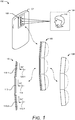
- FIG. 1 illustrates an example environment 100 in which an asymmetric sensor array for capturing images can be embodied.
- Example environment 100 includes an imaging device 102 capturing images of a scene 104.
- Imaging device 102 includes an imager 106, which includes lens stacks 108 and asymmetric sensor array 110, shown combined and separate.
- Asymmetric sensor array 302-1 includes a clear, high pixel-count main sensor and two color-pixel peripheral sensors with larger pixels but smaller overall physical size than that of the main sensor.
- Asymmetric sensor array 302-2 includes a clear, high pixel-count main sensor and four peripheral color-pixel sensors with same-size pixels as that of the main sensor.
- Asymmetric sensor array 302-3 includes a clear or a color high-pixel count main sensor and two large-sized and high-pixel count peripheral sensors with color pixels.
- Figure 7 illustrates various components of an example electronic device 700 that can be implemented as an imaging device as described with reference to any of the previous figures 1-6 .
- the electronic device may be implemented as any one or combination of a fixed or mobile device, in any form of a consumer, computer, portable, user, communication, phone, navigation, gaming, audio, camera, messaging, media playback, and/or other type of electronic device, such as imaging device 102 described with reference to figures 1 and 5 .
- a processing system may be implemented at least partially in hardware, which can include components of an integrated circuit or on-chip system, digital-signal processor (DSP), application-specific integrated circuit (ASIC), field-programmable gate array (FPGA), a complex programmable logic device (CPLD), and other implementations in silicon and/or other hardware.
- DSP digital-signal processor
- ASIC application-specific integrated circuit
- FPGA field-programmable gate array
- CPLD complex programmable logic device
Landscapes
- Engineering & Computer Science (AREA)
- Multimedia (AREA)
- Signal Processing (AREA)
- Studio Devices (AREA)
- Solid State Image Pick-Up Elements (AREA)
Description
- This background description is provided for the purpose of generally presenting the context of the disclosure. Unless otherwise indicated herein, material described in this section is neither expressly nor impliedly admitted to be prior art to the present disclosure or the appended claims.
- Current sensor arrays for capturing images have partially addressed the need for a small form factor in the Z dimension for cameras and other imaging devices. These conventional sensor arrays, however, have various limitations. First, images captured for each sensor of the array must be combined in some manner through computational effort to construct the final image, which has varied success and requires computing resources. Second, this construction of the final image can be scene-dependent, meaning that some scenes result in relatively poor image quality. Third, these conventional sensor arrays often struggle to provide high resolution images, especially if there are any flaws in the sensors or lenses.
EP 2 472 581 A2 discloses an apparatus for combining a mobile communication device with a camera that includes a curved sensor. The apparatus comprises mobile communication means including an enclosure and an objective lens. The objective lens is mounted on said enclosure and arranged to collect a stream of radiation. A curved sensor includes a plurality of sensor elements, where the curved sensor is mounted inside said enclosure and aligned with the objective lens. The curved sensor has a portion which extends beyond a generally two-dimensional plane and has an output for recording an image. The combination of a mobile communication device with a camera that utilizes a curved sensor offers higher quality pictures than conventional phones that incorporate a flat sensor.
US 2005/134712 A1 discloses a color image sensor having imaging element array forming images on respective regions of sensor elements. The color image sensor generates a color image signal representing a subject and includes an optical substrate and a light sensor. The optical substrate includes spatially-separated imaging elements. Each of the imaging elements is configured to image light of a respective color. The light sensor includes regions of sensor elements disposed opposite respective ones of the imaging elements. The sensor elements in each of the regions are operable to generate a component of the color image signal in response to the light of the respective color incident on them.
EP 2 451 150 A2 discloses a system for calibrating a color sensing pixel based upon the distance between the color sensing pixel and an object. The distance is determined by measuring the phase shift of electromagnetic radiation as reflected from the surface of the object compared with the wave profile of the electromagnetic radiation incident on the object surface. The color sensing pixel is associated with a Time-of-Flight (ToF) pixel which is employed to determine the distance of the color sensing pixel. The electromagnetic radiation can be from any part of the electromagnetic spectrum, in particular the infrared and visible light portions of the electromagnetic spectrum. The color sensing pixel and the ToF pixel can reside on the same semiconductor or on disparate semiconductors. - The solution is specified by an imaging device for capturing images of a scene as claimed in claim 1. Dependent claims specify embodiments thereof.
- Apparatuses of and techniques using an asymmetric sensor array for capturing images are described with reference to the following drawings. The same numbers are used throughout the drawings to reference like features and components:
-
Figure 1 illustrates an example environment in which an asymmetric sensor array for capturing images can be enabled. -
Figure 2 illustrates an example of an asymmetric sensor array offigure 1 , shown in both cross-section and plan views. -
Figure 3 illustrates alternative asymmetric sensor arrays, all shown in plan view. -
Figure 4 illustrates lens stacks of different Z-heights relative to sensor sizes of sensors in an asymmetric sensor array. -
Figure 5 illustrates the imaging device offigure 1 in greater detail. -
Figure 6 illustrates example methods that use an asymmetric sensor array to capture images and, with those images, create a final image. -
Figure 7 illustrates various components of an electronic device that can implement an asymmetric sensor array for capturing images in accordance with one or more embodiments. - Conventional sensor arrays use an array of equivalent image sensors to realize a final image. These sensor arrays enable a camera to have a low Z-height relative to the quality of the final image. Compared to a single sensor that provides a similar image quality, for example, sensor arrays have a low Z-height. This is due to a relationship between sensor size and Z height for the lens that focuses the image onto the sensor. Thus, a four-megapixel single sensor requires, assuming similar lens characteristics, a much taller Z height than an array of four one-megapixel sensors. Each of the four one-megapixel sensors is smaller and thus uses a shorter Z-height.
- These conventional sensor arrays, however, have various limitations, such as failing to realize sharp optics, depth of color, scene-independent image reconstruction, or low-light sensitivity.
- Consider, for example, a conventional sensor having a 2 x 2 grid of sensors, the sensors having red, green, green, and blue pixels to capture images. Each of the four sensors in the array includes small repeating squares having four pixels each, one pixel that senses red, one blue, and two green. The two green are used to determine resolution (e.g., sharpness) in addition to the color green. Mathematically, a one-megapixel sensor is then capable of one-half-megapixel resolution. Through various computational processes, which are not the topic of this disclosure, this one-half-megapixel resolution can be interpolated to improve the resolution (again, with varied success) by about 20%. Thus, the one-megapixel red, green, green, blue sensor can result in a final resolution of about 0.7 megapixels, though this final resolution has limitations as noted above.
- To maximize this resolution, conventional sensor arrays use small color pixels to increases a number of pixels in a sensor, and thus keep the size of the sensor down, which in turn keeps the Z-height relatively low. Small color pixels, however, often fail to handle noise well, as each pixel's ability is limited by size, and thus small pixels have poorer signal-to-noise ratios than large pixels. Conventional sensor arrays often forgo use of large pixels, however, because doing so increases the Z-height or reduces the final resolution of the image.
- Consider instead, however, an example asymmetric sensor array for capturing images. This asymmetric sensor array, instead of using small color pixels and equivalent sensors, uses an asymmetric sensor array having a central monochrome sensor for resolution and peripheral, relatively large color-pixel sensors for color. The central monochrome-pixel sensor provides high resolution using small pixels. The peripheral, large-pixel color sensors provide color and, due to their size, have excellent signal-to-noise ratios, and thus provide truer color, better color in low-light situations, or other benefits described below. While these peripheral color sensors have lower resolution than the central sensor, the human eye distinguishes less detail in color than it does in greyscale (e.g., the image's resolution or sharpness). Therefore, this asymmetric sensor array provides a final image that conforms to the human eye's characteristics - with high sharpness and truer color, as well as less sensitively to low-light and other adverse scene characteristics.
- The following discussion first describes an operating environment, then example asymmetric sensor arrays, then a detailed description of an example imaging device, followed by techniques that may be employed in this environment and imaging device, and ends with an example electronic device.
-
Figure 1 illustrates anexample environment 100 in which an asymmetric sensor array for capturing images can be embodied.Example environment 100 includes animaging device 102 capturing images of ascene 104.Imaging device 102 includes animager 106, which includes lens stacks 108 andasymmetric sensor array 110, shown combined and separate. -
Asymmetric sensor array 110 includes amain sensor 112 having a main resolution and angled at amain angle 114. Heremain angle 114, as shown relative to object 116 ofscene 104, is at ninety degrees.Asymmetric sensor array 110 also includes multiple peripheral sensors 118. These peripheral sensors 118 have peripheral resolutions or colors that are asymmetric to the main colors or resolution. Asymmetric sensors can be asymmetric to each other by having different numbers of pixels, color-sensing of pixels, sizes of pixels, or sensor size. - Peripheral sensors 118 (shown at 118-1 and 118-2) can be positioned at peripheral angles 120 (shown as peripheral angles 120-1 and 120-2, respectively), which are different from
main angle 114 ofmain sensor 112. This difference or differences in angles enables a depth of image to be created for an image of a scene based on peripheral data sensed by the one of the peripheral sensors of the scene and main data sensed by the main sensor of the same scene or different peripheral data sensed by a different peripheral sensor of the same scene, or some combination of these. Thus, peripheral angle 120-1 of 5° off ofmain angle 114 captures peripheral data through capture of an image ofobject 116 different from that of an image captured ofobject 116 frommain sensor 112 atmain angle 114. - Consider
figure 2 , which illustrates an example ofasymmetric sensor array 110 offigure 1 . Infigure 1 ,asymmetric sensor array 110 is shown oriented vertically and in cross section and is also shown atcross-section view 202 infigure 2 but oriented horizontally.Figure 2 illustrates, expanded and in aplan view 204,asymmetric sensor array 110. Note thatasymmetric sensor array 110 is structured such thatmain sensor 112 is centered between peripheral sensors 118. - As mentioned above,
main sensor 112 may include various resolutions and types. In the example offigure 2 ,main sensor 112 is monochrome with a clear color filter. This monochrome aspect improves signal-to-noise ratio in low-light situations and, as noted, enables a high detail for a given pixel count, though in monochrome (e.g., grayscale). Thus,main sensor 112 enables higher detail than color-pixel sensors.Main sensor 112 can also perform better in low-light environments due to an improved signal-to-noise ratio (SNR). In some cases,main sensor 112 also includes a filter permitting infrared radiation to be sensed bymain sensor 112. Typically infrared radiation is not desired for color-pixel sensors because infrared radiation inhibits color fidelity. Here, however,main sensor 112 is monochrome, and thus this typical limitation is not present. Further, by permitting infrared radiation to be sensed, the bandwidth captured by the imager is expanded into the near Infrared (IR). This also improve SNR in low-light scenes, in some cases so much thatmain sensor 112 may capture images in near darkness. IR sensing may, in some cases, permit a faster exposure time as well as better capture of moving objects in a scene, which can be useful for still images and for capture of multiple images in recording a video, especially for high-resolution capture of video. - This illustration shows resolutions of
main sensor 112 and peripheral sensors 118 in terms of a number and size of squares, which are here assumed to be pixels. While simplified for visual clarity (showing millions of pixels is not possible for this type of illustration),main sensor 112 includes four times the number of pixels of each of peripheral sensors 118, and peripheral sensors 118 include pixels that are four times as large as those ofmain sensor 112. - The estimation of a depth map for images (e.g., a per-pixel estimation of the distance between a camera and a scene) improves with image SNR. Given this, and the use of peripheral sensors 118 at some angle relative to
main sensor 112 for depth mapping, the larger size of pixels of peripheral sensors 118 can improve depth mapping by improving SNR. In more detail, smaller pixels have less capacity to absorb photons, and thus, they have less capacity to accept noise. Therefore, the larger pixels allow for a better signal-to-noise ratio, which aids in depth mapping for accurate color representation and for low-light scenes. - In addition to the example shown in
figure 2 , considerfigure 3 , which illustrates alternativeasymmetric sensor arrays 302, all shown in plan view. Asymmetric sensor array 302-1 includes a clear, high pixel-count main sensor and two color-pixel peripheral sensors with larger pixels but smaller overall physical size than that of the main sensor. Asymmetric sensor array 302-2 includes a clear, high pixel-count main sensor and four peripheral color-pixel sensors with same-size pixels as that of the main sensor. Asymmetric sensor array 302-3 includes a clear or a color high-pixel count main sensor and two large-sized and high-pixel count peripheral sensors with color pixels. The color sensors may be Bayer filter sensors, panchromatic cell sensors, improved or angled Bayer-type filter sensors (e.g., EXR and X-Trans by Fujifilm™), or other color-capturing sensors. The color sensors may sense a wide variety of colors and be structured with color pixels, such as red, green, green, and blue pixels arranged in squares, red, green, blue, and white also in squares, angled double-pixel colored (non-square) of cyan, magenta, and yellow or red, green, and blue of roughly equal amounts (rather than more green), and so forth. - Each of these
asymmetric sensor arrays - As noted for
figure 1 ,imaging device 102 includesimager 106, which includesasymmetric sensor array 110 and lens stacks 108.Figure 4 illustrates one oflens stacks 108 in detail to describe a relationship between sensor size and Z-height mentioned above. As shown, and assuming a similar lens material and physical structure, Z-height 402 is related (in some cases proportional) to dimensions of sensors, such asX-width 404 ofmain sensor 112. As shown, a height oflens 406, along with some distance to focus light (focal distance 408) makes up Z-height 402, which together are related to X-width 404 (as well as Y-breadth, not shown). -
Figure 4 also illustrates an exampleasymmetric sensor array 410 with amain sensor 412 having an X-width 414 related to a lens-stack height 416 and twoperipheral sensors 418 having a smaller X-width 420 related to a smaller lens-stack height 422. This illustration shows that a Z-height of an imager is related to sensor size (Y-breadth is illustrated and equal to respective X-widths). Aplan view 424 ofasymmetric sensor array 410 is also provided to show this relationship. While not required, in some cases main and peripheral sensors (e.g.,main sensor 412 and peripheral sensors 418) and integrated into a single die or substrate.Imager 106 may also be structured as an integrated apparatus, such as includingasymmetric sensor array 410 along with lens stacks for each of the sensors in the array. - While not shown, the various imagers may include, or
imaging device 102 may include separate from the various imagers, an auto-focus device capable of determining a focus of the main sensor in part using depth data captured by the peripheral sensors. This is not required, as in some cases no auto-focus is needed. Use of an auto-focus device can depend on a desired image quality and a size and resolution of sensors used to deliver this image quality. This can be balanced, however, with an undesirable focus lag of many current auto-focus mechanisms. The asymmetric sensor array, however, can reduce this focus lag by decreasing an iterative adjust and sense operation of current auto-focus systems. The iterative adjust and sense operation is decreased by using depth information captured by the peripheral sensors to guide the auto-focus system, thereby reducing a number of iterations required to achieve focus. - Furthermore, these various imagers can be structured to be capable of focusing at objects in scenes beyond about two meters from the lens of the main sensor without a focusing mechanism. If focusing on objects within two meters is desired, a simpler optical system to adjust focus only at near-field scenes (objects within one to two meters) can be used. This simpler optical system can be a near-far toggle, for example.
- Having generally described asymmetric sensor arrays and imagers, this discussion now turns to
figure 5 , which illustratesimaging device 102 offigure 1 in greater detail.Imaging device 102 is illustrated with various non-limiting example devices: smartphone 102-1, laptop 102-2, television 102-3, desktop 102-4, tablet 102-5, and camera 102-6.Imaging device 102 includes processor(s) 504 and computer-readable media 506, which includesmemory media 508 andstorage media 510. Applications and/or an operating system (not shown) embodied as computer-readable instructions on computer-readable memory 506 can be executed by processor(s) 504 to provide some or all of the functionalities described herein. Computer-readable media 506 also includesimage manager 512. As noted above,imaging device 102 includesimager 106, which in turn includes lens stacks 108 andasymmetric sensor array 110, and in some cases a focusingmodule 514, which may be software or hardware or both (e.g., as an above-mentioned auto-focus system). - In some cases,
imaging device 102 is in communication with, but may not necessarily include,imager 106 or elements thereof. Captured images are then received byimaging device 102 fromimager 106 via the one or more I/O ports 516. I/O ports 516 can include a variety of ports, such as by way of example and not limitation, high-definition multimedia (HDMI), digital video interface (DVI), display port, fiber-optic or light-based, audio ports (e.g., analog, optical, or digital), USB ports, serial advanced technology attachment (SATA) ports, peripheral component interconnect (PCI) express based ports or card slots, serial ports, parallel ports, or other legacy ports.Imaging device 102 may also include network interface(s) 518 for communicating data over wired, wireless, or optical networks. By way of example and not limitation,network interface 518 may communicate data over a local-area-network (LAN), a wireless local-area-network (WLAN), a personal-area-network (PAN), a wide-area-network (WAN), an intranet, the Internet, a peer-to-peer network, point-to-point network, a mesh network, and the like. - The following discussion describes methods by which techniques are implemented to enable use of asymmetric sensor arrays for capturing images. These methods can be implemented utilizing the previously described environment and example sensor arrays and imagers, such as shown in
figures 1-5 . Aspects of these example methods are illustrated infigure 6 , which are shown as operations performed by one or more entities. The orders in which operations of these methods are shown and/or described are not intended to be construed as a limitation, and any number or combination of the described method operations can be combined in any order to implement a method, or an alternate method. -
Figure 6 illustratesexample methods 600 using an asymmetric sensor array to capturing images and, with those images, create a final image. At 602, sensor data is received from a main sensor of an asymmetric sensor array. The main sensor, as noted above, may be monochromatic, and thus the sensor data include a high-resolution, monochromatic image of a scene. Usingimaging device 102 offigures 1 and5 as an example,image manager 512 receives, frommain sensor 112, sensordata capturing scene 104 andobject 116. Assuming also thatmain sensor 112 and peripheral sensors 118 are as shown infigure 2 ,main sensor 112 provides sensor data that is monochromatic and high resolution with good data for low-light scenes. - At 604, peripheral sensor data including multiple color images of the scene are received from peripheral sensors. One or more of the multiple color images can be sensed at an angle different than the angle of reception of the sensor data of the main sensor. As noted above, this different angle enables creation of a depth map along with other uses also described above. Also, in some example asymmetric sensor arrays, such as
asymmetric sensor array 110, 302-1, and 302-2 (but not 302-3), offigures 2 and3 , respectively, the color images are low resolution relative to the resolution of the main sensor. - Continuing the ongoing example, peripheral sensor data from peripheral sensors 118 include two low-resolution color images of
scene 104, both of which are sensed at angles different from those ofmain sensor 112, namely by five degrees (seefigure 1 ), though other angles may instead be used. - At 606, a depth map is determined based on the multiple color images. This depth map includes information relating to distances of surfaces in a sense (such as
object 116 ofscene 104 offigure 1 ), though these distances may be relative to a focal plane, other objects in the scene, or the imager or sensors. Hereimage manager 512 offigure 5 receives the sensor data frommain sensor 112 and peripheral sensor data from peripheral sensors 118.Image manager 512 then determines the depth map based on the color images being sensed at different angles from the main sensor's high-resolution image (whether color or monochrome). - At 608, a final image is constructed using the depth map, the multiple color images, and the high-resolution image.
Image manager 512, for example, may "paint" the low-resolution color images from peripheral sensors 118 onto the high-resolution, monochromatic image frommain sensor 112, in part with use of the depth map. By so doing,methods 600 create a finalimage having object 116 in focus, with high sharpness, accurate color and depth of color, and, in many cases, using fewer computation resources or more quickly (in focusing or processing). -
Figure 7 illustrates various components of an exampleelectronic device 700 that can be implemented as an imaging device as described with reference to any of the previousfigures 1-6 . The electronic device may be implemented as any one or combination of a fixed or mobile device, in any form of a consumer, computer, portable, user, communication, phone, navigation, gaming, audio, camera, messaging, media playback, and/or other type of electronic device, such asimaging device 102 described with reference tofigures 1 and5 . -
Electronic device 700 includescommunication transceivers 702 that enable wired and/or wireless communication of device data 704, such as received data, transmitted data, or sensor data as described above. Example communication transceivers include NFC transceivers, WPAN radios compliant with various IEEE 802.15 (Bluetooth™) standards, WLAN radios compliant with any of the various IEEE 802.11 (WiFi™) standards, WWAN (3GPP-compliant) radios for cellular telephony, wireless metropolitan area network (WMAN) radios compliant with various IEEE 802.16 (WiMAX™) standards, and wired local area network (LAN) Ethernet transceivers. -
Electronic device 700 may also include one or more data input ports 706 via which any type of data, media content, and/or inputs can be received, such as user-selectable inputs, messages, music, television content, recorded video content, and any other type of audio, video, and/or image data received from any content and/or data source (e.g., other image devices or imagers). Data input ports 706 may include USB ports, coaxial cable ports, and other serial or parallel connectors (including internal connectors) for flash memory, DVDs, CDs, and the like. These data input ports may be used to couple the electronic device to components (e.g., imager 106), peripherals, or accessories such as keyboards, microphones, or cameras. -
Electronic device 700 of this example includes processor system 708 (e.g., any of application processors, microprocessors, digital-signal-processors, controllers, and the like), or a processor and memory system (e.g., implemented in a SoC), which process (i.e., execute) computer-executable instructions to control operation of the device. Processor system 708 (processor(s) 708) may be implemented as an application processor, embedded controller, microcontroller, and the like. A processing system may be implemented at least partially in hardware, which can include components of an integrated circuit or on-chip system, digital-signal processor (DSP), application-specific integrated circuit (ASIC), field-programmable gate array (FPGA), a complex programmable logic device (CPLD), and other implementations in silicon and/or other hardware. - Alternatively or in addition,
electronic device 700 can be implemented with any one or combination of software, hardware, firmware, or fixed logic circuitry that is implemented in connection with processing and control circuits, which are generally identified at 710 (processing and control 710). Hardware-only devices in which an asymmetric sensor array for capturing images may be embodied include those that convert, without computer processors, sensor data into voltage signals by which to control focusing systems (e.g., focusing module 514). - Although not shown,
electronic device 700 can include a system bus, crossbar, or data transfer system that couples the various components within the device. A system bus can include any one or combination of different bus structures, such as a memory bus or memory controller, a peripheral bus, a universal serial bus, and/or a processor or local bus that utilizes any of a variety of bus architectures. -
Electronic device 700 also includes one ormore memory devices 712 that enable data storage, examples of which include random access memory (RAM), non-volatile memory (e.g., read-only memory (ROM), flash memory, EPROM, EEPROM, etc.), and a disk storage device. Memory device(s) 712 provide data storage mechanisms to store the device data 704, other types of information and/or data, and various device applications 720 (e.g., software applications). For example,operating system 714 can be maintained as software instructions withinmemory device 712 and executed byprocessors 708. In some aspects,image manager 512 is embodied inmemory devices 712 ofelectronic device 700 as executable instructions or code. Although represented as a software implementation,image manager 512 may be implemented as any form of a control application, software application, signal-processing and control module, or hardware or firmware installed onimager 106. -
Electronic device 700 also includes audio and/orvideo processing system 716 that processes audio data and/or passes through the audio and video data to audio system 718 and/or to display system 722 (e.g., a screen of a smart phone or camera). Audio system 718 and/ordisplay system 722 may include any devices that process, display, and/or otherwise render audio, video, display, and/or image data. Display data and audio signals can be communicated to an audio component and/or to a display component via an RF (radio frequency) link, S-video link, HDMI (high-definition multimedia interface), composite video link, component video link, DVI (digital video interface), analog audio connection, or other similar communication link, such asmedia data port 724. In some implementations, audio system 718 and/ordisplay system 722 are external components toelectronic device 700. Alternatively or additionally,display system 722 can be an integrated component of the example electronic device, such as part of an integrated touch interface.Electronic device 700 includes, or has access to,imager 106, which includes lens stacks 108 and asymmetric sensor array 110 (or 302 or 410). Sensor data is received fromimager 106 and/orasymmetric sensor array 110 byimage manager 512, here shown stored inmemory devices 712, which when executed byprocessor 708 constructs a final image as noted above. - Although embodiment of an asymmetric sensor array for capturing images have been described in language specific to features and/or methods, the subject of the appended claims is not necessarily limited to the specific features or methods described. Rather, the specific features and methods are disclosed as example implementations an asymmetric sensor array for capturing images.
Claims (10)
- An imaging device for capturing images of a scene (104) comprising:an imager (106), the imager (106) comprising:an asymmetric sensor array (110, 410) having within a single die or substrate a main sensor (112, 412) and two or more peripheral sensors (118, 418), wherein the main sensor (112, 412) has a main resolution and is angled at a main angle (114) relative to an object (116) of the scene (104) and the two or more peripheral sensors (118, 418) have peripheral resolutions being asymmetric to the main resolution by having at least one of a different number of pixels, different color-sensing of pixels, different size of pixels or different sensor size and are positioned at peripheral angles (120) relative to the object (116) of the scene (104) different from the main angle (114) of the main sensor (112, 412); anda lens stack (108) for each of the main and peripheral sensors (112, 412, 118, 418);one or more computer processors (504, 408); andone or more computer-readable storage media (506) having instructions stored thereon that, responsive to execution by the one or more computer processors (504), implements an image manager capable of performing operations comprising:receiving, from the main sensor (112, 412), sensor data, the sensor data including a high-resolution, monochromatic image of a scene (104);receiving, from the peripheral sensors (118, 418), peripheral sensor data, the peripheral sensor data including multiple low-resolution color images of the scene (104), at least one of the multiple low-resolution color images being sensed at an angle different than an angle of reception of the sensor data of the main sensor (112, 412);determining, based on at least one of the multiple low-resolution color images of the scene (104) being sensed at different angles from the main sensor and on the monochromatic high-resolution image of the same scene (104), being sensed by the main sensor, a depth map; andconstructing a final image using the low-resolution color images, the depth map, and the monochromatic high-resolution image.
- The imaging device as recited in claim 1, wherein the main resolution is a first number of pixels and the peripheral resolutions are each a second number of pixels, the first number of pixels being larger than the second number of pixels.
- The imaging device as recited in claim 1, wherein the main sensor (112, 412) includes a first size of pixels and the peripheral sensors (118, 418) include a second size of pixels, the first size smaller than the second size.
- The imaging device as recited in claim 1, wherein the main sensor (112, 412) is a monochrome with a clear color filter.
- The imaging device as recited in claim 1, wherein the main sensor (112, 412) includes a filter permitting infrared radiation to be sensed by the main sensor (112, 412).
- The imaging device as recited in claim 1, wherein the main sensor (112, 412) is centered between the peripheral sensors (118, 418).
- The imaging device as recited in claim 6, wherein the peripheral sensors (118, 418) include two or four peripheral sensors (118, 418).
- The imaging device as recited in claim 1, wherein the peripheral sensors (118, 418) are Bayer sensors.
- The imaging device of claim 1, wherein the final image includes a high-resolution of the high-resolution, monochromatic image and colors of the multiple low-resolution color images, and/or
wherein pixels of the peripheral sensors (118, 418) are larger than pixels of the main sensor (112, 412), and/or
wherein the imaging device (102) is capable of constructing, without a focusing mechanism, the final image in focus for objects of a scene (104) that are beyond two meters from the imager. - The imaging device of claim 1, further comprising a near-far toggle focus system.
Applications Claiming Priority (2)
| Application Number | Priority Date | Filing Date | Title |
|---|---|---|---|
| US201361856449P | 2013-07-19 | 2013-07-19 | |
| PCT/US2014/047313 WO2015010098A1 (en) | 2013-07-19 | 2014-07-18 | Asymmetric sensor array for capturing images |
Publications (2)
| Publication Number | Publication Date |
|---|---|
| EP3022898A1 EP3022898A1 (en) | 2016-05-25 |
| EP3022898B1 true EP3022898B1 (en) | 2020-04-15 |
Family
ID=51492421
Family Applications (1)
| Application Number | Title | Priority Date | Filing Date |
|---|---|---|---|
| EP14772236.7A Active EP3022898B1 (en) | 2013-07-19 | 2014-07-18 | Asymmetric sensor array for capturing images |
Country Status (4)
| Country | Link |
|---|---|
| US (1) | US20150022643A1 (en) |
| EP (1) | EP3022898B1 (en) |
| CN (1) | CN105308953A (en) |
| WO (1) | WO2015010098A1 (en) |
Families Citing this family (29)
| Publication number | Priority date | Publication date | Assignee | Title |
|---|---|---|---|---|
| US10591969B2 (en) | 2013-10-25 | 2020-03-17 | Google Technology Holdings LLC | Sensor-based near-field communication authentication |
| US9414037B1 (en) * | 2014-09-26 | 2016-08-09 | Amazon Technologies, Inc. | Low light image registration |
| US9894298B1 (en) | 2014-09-26 | 2018-02-13 | Amazon Technologies, Inc. | Low light image processing |
| US9936129B2 (en) | 2016-06-15 | 2018-04-03 | Obsidian Sensors, Inc. | Generating high resolution images |
| US10341628B2 (en) * | 2016-08-08 | 2019-07-02 | Google Llc | Monochrome-color mapping using a monochromatic imager and a color map sensor |
| US10451714B2 (en) | 2016-12-06 | 2019-10-22 | Sony Corporation | Optical micromesh for computerized devices |
| US10536684B2 (en) | 2016-12-07 | 2020-01-14 | Sony Corporation | Color noise reduction in 3D depth map |
| US10181089B2 (en) | 2016-12-19 | 2019-01-15 | Sony Corporation | Using pattern recognition to reduce noise in a 3D map |
| US10178370B2 (en) | 2016-12-19 | 2019-01-08 | Sony Corporation | Using multiple cameras to stitch a consolidated 3D depth map |
| US10495735B2 (en) | 2017-02-14 | 2019-12-03 | Sony Corporation | Using micro mirrors to improve the field of view of a 3D depth map |
| US10795022B2 (en) | 2017-03-02 | 2020-10-06 | Sony Corporation | 3D depth map |
| US10979687B2 (en) | 2017-04-03 | 2021-04-13 | Sony Corporation | Using super imposition to render a 3D depth map |
| US20200126220A1 (en) * | 2017-06-26 | 2020-04-23 | Sony Corporation | Surgical imaging system and signal processing device of surgical image |
| US10930709B2 (en) | 2017-10-03 | 2021-02-23 | Lockheed Martin Corporation | Stacked transparent pixel structures for image sensors |
| US11678035B2 (en) | 2017-10-05 | 2023-06-13 | University Of Utah Research Foundation | Translucent imaging systems and related methods |
| US10484667B2 (en) | 2017-10-31 | 2019-11-19 | Sony Corporation | Generating 3D depth map using parallax |
| US10510812B2 (en) | 2017-11-09 | 2019-12-17 | Lockheed Martin Corporation | Display-integrated infrared emitter and sensor structures |
| US10838250B2 (en) | 2018-02-07 | 2020-11-17 | Lockheed Martin Corporation | Display assemblies with electronically emulated transparency |
| US11616941B2 (en) | 2018-02-07 | 2023-03-28 | Lockheed Martin Corporation | Direct camera-to-display system |
| US10690910B2 (en) | 2018-02-07 | 2020-06-23 | Lockheed Martin Corporation | Plenoptic cellular vision correction |
| US10979699B2 (en) | 2018-02-07 | 2021-04-13 | Lockheed Martin Corporation | Plenoptic cellular imaging system |
| US10951883B2 (en) | 2018-02-07 | 2021-03-16 | Lockheed Martin Corporation | Distributed multi-screen array for high density display |
| US10594951B2 (en) * | 2018-02-07 | 2020-03-17 | Lockheed Martin Corporation | Distributed multi-aperture camera array |
| US10652529B2 (en) | 2018-02-07 | 2020-05-12 | Lockheed Martin Corporation | In-layer Signal processing |
| KR102486425B1 (en) * | 2018-02-23 | 2023-01-09 | 엘지이노텍 주식회사 | Camera module and super resolution image processing method performed therein |
| CN108377325A (en) * | 2018-05-21 | 2018-08-07 | Oppo广东移动通信有限公司 | Shooting device, electronic device and image acquisition method |
| US10549186B2 (en) | 2018-06-26 | 2020-02-04 | Sony Interactive Entertainment Inc. | Multipoint SLAM capture |
| US10866413B2 (en) | 2018-12-03 | 2020-12-15 | Lockheed Martin Corporation | Eccentric incident luminance pupil tracking |
| US10698201B1 (en) | 2019-04-02 | 2020-06-30 | Lockheed Martin Corporation | Plenoptic cellular axis redirection |
Family Cites Families (19)
| Publication number | Priority date | Publication date | Assignee | Title |
|---|---|---|---|---|
| US7511749B2 (en) * | 2003-12-18 | 2009-03-31 | Aptina Imaging Corporation | Color image sensor having imaging element array forming images on respective regions of sensor elements |
| US7791638B2 (en) * | 2004-09-29 | 2010-09-07 | Immersive Media Co. | Rotating scan camera |
| US7469097B2 (en) * | 2005-12-15 | 2008-12-23 | Hewlett-Packard Development Company, L.P. | Method and apparatus for coping with condition in which subject is too close to digital imaging device for acceptable focus |
| US7507944B1 (en) * | 2006-06-27 | 2009-03-24 | Cypress Semiconductor Corporation | Non-planar packaging of image sensor |
| US7733397B2 (en) * | 2006-12-22 | 2010-06-08 | Palo Alto Research Center Incorporated | Sensor surface with 3D curvature formed by electronics on a continuous 2D flexible substrate |
| FR2914811B1 (en) * | 2007-04-06 | 2010-04-30 | Sagem Defense Securite | OPTICAL DEVICE COMPRISING AT LEAST TWO SENSORS, METHOD FOR IMPLEMENTING THE SAME |
| DE102007054156A1 (en) * | 2007-11-12 | 2009-05-14 | Ventech Gmbh | Method for determining the pressure and the tread depth in a vehicle tire |
| JP2011523538A (en) * | 2008-05-20 | 2011-08-11 | ペリカン イメージング コーポレイション | Image capture and processing using monolithic camera arrays with different types of imagers |
| US8654215B2 (en) * | 2009-02-23 | 2014-02-18 | Gary Edwin Sutton | Mobile communicator with curved sensor camera |
| EP2388987A1 (en) * | 2010-05-19 | 2011-11-23 | Thomson Licensing | Camera with volumetric sensor chip |
| US20140192238A1 (en) * | 2010-10-24 | 2014-07-10 | Linx Computational Imaging Ltd. | System and Method for Imaging and Image Processing |
| US8542348B2 (en) * | 2010-11-03 | 2013-09-24 | Rockwell Automation Technologies, Inc. | Color sensor insensitive to distance variations |
| CN102087357B (en) * | 2010-12-18 | 2012-11-28 | 浙江大学 | Method for echo direction estimation of sensor array and for multibeam echo depth sounding and bottom detection |
| US8717467B2 (en) * | 2011-01-25 | 2014-05-06 | Aptina Imaging Corporation | Imaging systems with array cameras for depth sensing |
| JP5398750B2 (en) * | 2011-01-26 | 2014-01-29 | 株式会社東芝 | The camera module |
| US8937646B1 (en) * | 2011-10-05 | 2015-01-20 | Amazon Technologies, Inc. | Stereo imaging using disparate imaging devices |
| US9846960B2 (en) * | 2012-05-31 | 2017-12-19 | Microsoft Technology Licensing, Llc | Automated camera array calibration |
| US9729857B2 (en) * | 2014-04-08 | 2017-08-08 | Semyon Nisenzon | High resolution depth map computation using multiresolution camera clusters for 3D image generation |
| KR102269599B1 (en) * | 2014-04-23 | 2021-06-25 | 삼성전자주식회사 | Image pickup apparatus including lens elements having different diameters |
-
2014
- 2014-07-18 US US14/335,841 patent/US20150022643A1/en not_active Abandoned
- 2014-07-18 EP EP14772236.7A patent/EP3022898B1/en active Active
- 2014-07-18 WO PCT/US2014/047313 patent/WO2015010098A1/en not_active Ceased
- 2014-07-18 CN CN201480034086.8A patent/CN105308953A/en active Pending
Non-Patent Citations (1)
| Title |
|---|
| None * |
Also Published As
| Publication number | Publication date |
|---|---|
| US20150022643A1 (en) | 2015-01-22 |
| CN105308953A (en) | 2016-02-03 |
| WO2015010098A1 (en) | 2015-01-22 |
| EP3022898A1 (en) | 2016-05-25 |
Similar Documents
| Publication | Publication Date | Title |
|---|---|---|
| US20150022643A1 (en) | Asymmetric Sensor Array for Capturing Images | |
| US9343492B2 (en) | CMOS image sensor based on thin-film on asic and operating method thereof | |
| US10044926B2 (en) | Optimized phase detection autofocus (PDAF) processing | |
| US10341628B2 (en) | Monochrome-color mapping using a monochromatic imager and a color map sensor | |
| JP6598507B2 (en) | Imaging apparatus, imaging system, and signal processing method | |
| US10165167B2 (en) | Non-canting VCM-actuated autofocus | |
| JP5690977B2 (en) | Imaging device and imaging apparatus | |
| US9560298B2 (en) | Curved image sensor for a curved focal surface | |
| US9551856B2 (en) | MEMS-released curved image sensor | |
| US12267604B2 (en) | Image acquisition apparatus including a plurality of image sensors, and electronic apparatus including the image acquisition apparatus | |
| WO2014159758A1 (en) | System architecture for thermal imaging and thermography cameras | |
| US11997405B2 (en) | Electronic device integrating phase difference detection and imaging and method for controlling the same | |
| JP5677625B2 (en) | Signal processing apparatus, imaging apparatus, and signal correction method | |
| GB2554794B (en) | Monochrome-color mapping using a monochromatic imager and a color map sensor. | |
| TW202332252A (en) | Multi-sensor imaging color correction | |
| JP5542248B2 (en) | Imaging device and imaging apparatus | |
| JP5978415B2 (en) | Imaging apparatus and focus control method | |
| US20260033025A1 (en) | Image sensor using metasurface layer routing | |
| KR20260023426A (en) | Electronic device, method, and non-transitory computer readable storage medium for capturing image with wide angle of view | |
| WO2025069522A1 (en) | Information processing device, imaging device, information processing method, and information processing program | |
| KR20250059147A (en) | Image acquisition apparatus and electronic apparatus including the same | |
| KR20260038748A (en) | Electronic apparatus of processing image and operating method thereof | |
| CN120604522A (en) | Electronic device for acquiring images through image sensor and method for operating the same |
Legal Events
| Date | Code | Title | Description |
|---|---|---|---|
| PUAI | Public reference made under article 153(3) epc to a published international application that has entered the european phase |
Free format text: ORIGINAL CODE: 0009012 |
|
| 17P | Request for examination filed |
Effective date: 20151218 |
|
| AK | Designated contracting states |
Kind code of ref document: A1 Designated state(s): AL AT BE BG CH CY CZ DE DK EE ES FI FR GB GR HR HU IE IS IT LI LT LU LV MC MK MT NL NO PL PT RO RS SE SI SK SM TR |
|
| AX | Request for extension of the european patent |
Extension state: BA ME |
|
| DAX | Request for extension of the european patent (deleted) | ||
| STAA | Information on the status of an ep patent application or granted ep patent |
Free format text: STATUS: EXAMINATION IS IN PROGRESS |
|
| 17Q | First examination report despatched |
Effective date: 20171219 |
|
| REG | Reference to a national code |
Ref country code: DE Ref legal event code: R079 Ref document number: 602014063815 Country of ref document: DE Free format text: PREVIOUS MAIN CLASS: H04N0005369000 Ipc: H01L0027146000 |
|
| RIC1 | Information provided on ipc code assigned before grant |
Ipc: H04N 5/33 20060101ALI20191011BHEP Ipc: H04N 5/369 20110101ALI20191011BHEP Ipc: H04N 9/09 20060101ALI20191011BHEP Ipc: H04N 5/225 20060101ALI20191011BHEP Ipc: H01L 27/146 20060101AFI20191011BHEP |
|
| GRAP | Despatch of communication of intention to grant a patent |
Free format text: ORIGINAL CODE: EPIDOSNIGR1 |
|
| STAA | Information on the status of an ep patent application or granted ep patent |
Free format text: STATUS: GRANT OF PATENT IS INTENDED |
|
| INTG | Intention to grant announced |
Effective date: 20191122 |
|
| GRAS | Grant fee paid |
Free format text: ORIGINAL CODE: EPIDOSNIGR3 |
|
| GRAA | (expected) grant |
Free format text: ORIGINAL CODE: 0009210 |
|
| STAA | Information on the status of an ep patent application or granted ep patent |
Free format text: STATUS: THE PATENT HAS BEEN GRANTED |
|
| AK | Designated contracting states |
Kind code of ref document: B1 Designated state(s): AL AT BE BG CH CY CZ DE DK EE ES FI FR GB GR HR HU IE IS IT LI LT LU LV MC MK MT NL NO PL PT RO RS SE SI SK SM TR |
|
| REG | Reference to a national code |
Ref country code: CH Ref legal event code: EP |
|
| REG | Reference to a national code |
Ref country code: DE Ref legal event code: R096 Ref document number: 602014063815 Country of ref document: DE |
|
| REG | Reference to a national code |
Ref country code: IE Ref legal event code: FG4D |
|
| REG | Reference to a national code |
Ref country code: AT Ref legal event code: REF Ref document number: 1258300 Country of ref document: AT Kind code of ref document: T Effective date: 20200515 |
|
| REG | Reference to a national code |
Ref country code: NL Ref legal event code: FP |
|
| REG | Reference to a national code |
Ref country code: LT Ref legal event code: MG4D |
|
| PG25 | Lapsed in a contracting state [announced via postgrant information from national office to epo] |
Ref country code: NO Free format text: LAPSE BECAUSE OF FAILURE TO SUBMIT A TRANSLATION OF THE DESCRIPTION OR TO PAY THE FEE WITHIN THE PRESCRIBED TIME-LIMIT Effective date: 20200715 Ref country code: FI Free format text: LAPSE BECAUSE OF FAILURE TO SUBMIT A TRANSLATION OF THE DESCRIPTION OR TO PAY THE FEE WITHIN THE PRESCRIBED TIME-LIMIT Effective date: 20200415 Ref country code: GR Free format text: LAPSE BECAUSE OF FAILURE TO SUBMIT A TRANSLATION OF THE DESCRIPTION OR TO PAY THE FEE WITHIN THE PRESCRIBED TIME-LIMIT Effective date: 20200716 Ref country code: IS Free format text: LAPSE BECAUSE OF FAILURE TO SUBMIT A TRANSLATION OF THE DESCRIPTION OR TO PAY THE FEE WITHIN THE PRESCRIBED TIME-LIMIT Effective date: 20200815 Ref country code: PT Free format text: LAPSE BECAUSE OF FAILURE TO SUBMIT A TRANSLATION OF THE DESCRIPTION OR TO PAY THE FEE WITHIN THE PRESCRIBED TIME-LIMIT Effective date: 20200817 Ref country code: SE Free format text: LAPSE BECAUSE OF FAILURE TO SUBMIT A TRANSLATION OF THE DESCRIPTION OR TO PAY THE FEE WITHIN THE PRESCRIBED TIME-LIMIT Effective date: 20200415 Ref country code: LT Free format text: LAPSE BECAUSE OF FAILURE TO SUBMIT A TRANSLATION OF THE DESCRIPTION OR TO PAY THE FEE WITHIN THE PRESCRIBED TIME-LIMIT Effective date: 20200415 |
|
| REG | Reference to a national code |
Ref country code: AT Ref legal event code: MK05 Ref document number: 1258300 Country of ref document: AT Kind code of ref document: T Effective date: 20200415 |
|
| PG25 | Lapsed in a contracting state [announced via postgrant information from national office to epo] |
Ref country code: BG Free format text: LAPSE BECAUSE OF FAILURE TO SUBMIT A TRANSLATION OF THE DESCRIPTION OR TO PAY THE FEE WITHIN THE PRESCRIBED TIME-LIMIT Effective date: 20200715 Ref country code: RS Free format text: LAPSE BECAUSE OF FAILURE TO SUBMIT A TRANSLATION OF THE DESCRIPTION OR TO PAY THE FEE WITHIN THE PRESCRIBED TIME-LIMIT Effective date: 20200415 Ref country code: LV Free format text: LAPSE BECAUSE OF FAILURE TO SUBMIT A TRANSLATION OF THE DESCRIPTION OR TO PAY THE FEE WITHIN THE PRESCRIBED TIME-LIMIT Effective date: 20200415 Ref country code: HR Free format text: LAPSE BECAUSE OF FAILURE TO SUBMIT A TRANSLATION OF THE DESCRIPTION OR TO PAY THE FEE WITHIN THE PRESCRIBED TIME-LIMIT Effective date: 20200415 |
|
| PG25 | Lapsed in a contracting state [announced via postgrant information from national office to epo] |
Ref country code: AL Free format text: LAPSE BECAUSE OF FAILURE TO SUBMIT A TRANSLATION OF THE DESCRIPTION OR TO PAY THE FEE WITHIN THE PRESCRIBED TIME-LIMIT Effective date: 20200415 |
|
| REG | Reference to a national code |
Ref country code: DE Ref legal event code: R097 Ref document number: 602014063815 Country of ref document: DE |
|
| PG25 | Lapsed in a contracting state [announced via postgrant information from national office to epo] |
Ref country code: ES Free format text: LAPSE BECAUSE OF FAILURE TO SUBMIT A TRANSLATION OF THE DESCRIPTION OR TO PAY THE FEE WITHIN THE PRESCRIBED TIME-LIMIT Effective date: 20200415 Ref country code: CZ Free format text: LAPSE BECAUSE OF FAILURE TO SUBMIT A TRANSLATION OF THE DESCRIPTION OR TO PAY THE FEE WITHIN THE PRESCRIBED TIME-LIMIT Effective date: 20200415 Ref country code: DK Free format text: LAPSE BECAUSE OF FAILURE TO SUBMIT A TRANSLATION OF THE DESCRIPTION OR TO PAY THE FEE WITHIN THE PRESCRIBED TIME-LIMIT Effective date: 20200415 Ref country code: EE Free format text: LAPSE BECAUSE OF FAILURE TO SUBMIT A TRANSLATION OF THE DESCRIPTION OR TO PAY THE FEE WITHIN THE PRESCRIBED TIME-LIMIT Effective date: 20200415 Ref country code: IT Free format text: LAPSE BECAUSE OF FAILURE TO SUBMIT A TRANSLATION OF THE DESCRIPTION OR TO PAY THE FEE WITHIN THE PRESCRIBED TIME-LIMIT Effective date: 20200415 Ref country code: SM Free format text: LAPSE BECAUSE OF FAILURE TO SUBMIT A TRANSLATION OF THE DESCRIPTION OR TO PAY THE FEE WITHIN THE PRESCRIBED TIME-LIMIT Effective date: 20200415 Ref country code: AT Free format text: LAPSE BECAUSE OF FAILURE TO SUBMIT A TRANSLATION OF THE DESCRIPTION OR TO PAY THE FEE WITHIN THE PRESCRIBED TIME-LIMIT Effective date: 20200415 Ref country code: RO Free format text: LAPSE BECAUSE OF FAILURE TO SUBMIT A TRANSLATION OF THE DESCRIPTION OR TO PAY THE FEE WITHIN THE PRESCRIBED TIME-LIMIT Effective date: 20200415 |
|
| PLBE | No opposition filed within time limit |
Free format text: ORIGINAL CODE: 0009261 |
|
| STAA | Information on the status of an ep patent application or granted ep patent |
Free format text: STATUS: NO OPPOSITION FILED WITHIN TIME LIMIT |
|
| PG25 | Lapsed in a contracting state [announced via postgrant information from national office to epo] |
Ref country code: MC Free format text: LAPSE BECAUSE OF FAILURE TO SUBMIT A TRANSLATION OF THE DESCRIPTION OR TO PAY THE FEE WITHIN THE PRESCRIBED TIME-LIMIT Effective date: 20200415 Ref country code: SK Free format text: LAPSE BECAUSE OF FAILURE TO SUBMIT A TRANSLATION OF THE DESCRIPTION OR TO PAY THE FEE WITHIN THE PRESCRIBED TIME-LIMIT Effective date: 20200415 Ref country code: PL Free format text: LAPSE BECAUSE OF FAILURE TO SUBMIT A TRANSLATION OF THE DESCRIPTION OR TO PAY THE FEE WITHIN THE PRESCRIBED TIME-LIMIT Effective date: 20200415 |
|
| REG | Reference to a national code |
Ref country code: CH Ref legal event code: PL |
|
| 26N | No opposition filed |
Effective date: 20210118 |
|
| REG | Reference to a national code |
Ref country code: BE Ref legal event code: MM Effective date: 20200731 |
|
| PG25 | Lapsed in a contracting state [announced via postgrant information from national office to epo] |
Ref country code: LU Free format text: LAPSE BECAUSE OF NON-PAYMENT OF DUE FEES Effective date: 20200718 Ref country code: FR Free format text: LAPSE BECAUSE OF NON-PAYMENT OF DUE FEES Effective date: 20200731 Ref country code: LI Free format text: LAPSE BECAUSE OF NON-PAYMENT OF DUE FEES Effective date: 20200731 Ref country code: CH Free format text: LAPSE BECAUSE OF NON-PAYMENT OF DUE FEES Effective date: 20200731 |
|
| PG25 | Lapsed in a contracting state [announced via postgrant information from national office to epo] |
Ref country code: SI Free format text: LAPSE BECAUSE OF FAILURE TO SUBMIT A TRANSLATION OF THE DESCRIPTION OR TO PAY THE FEE WITHIN THE PRESCRIBED TIME-LIMIT Effective date: 20200415 Ref country code: BE Free format text: LAPSE BECAUSE OF NON-PAYMENT OF DUE FEES Effective date: 20200731 |
|
| PG25 | Lapsed in a contracting state [announced via postgrant information from national office to epo] |
Ref country code: IE Free format text: LAPSE BECAUSE OF NON-PAYMENT OF DUE FEES Effective date: 20200718 |
|
| PG25 | Lapsed in a contracting state [announced via postgrant information from national office to epo] |
Ref country code: TR Free format text: LAPSE BECAUSE OF FAILURE TO SUBMIT A TRANSLATION OF THE DESCRIPTION OR TO PAY THE FEE WITHIN THE PRESCRIBED TIME-LIMIT Effective date: 20200415 Ref country code: MT Free format text: LAPSE BECAUSE OF FAILURE TO SUBMIT A TRANSLATION OF THE DESCRIPTION OR TO PAY THE FEE WITHIN THE PRESCRIBED TIME-LIMIT Effective date: 20200415 Ref country code: CY Free format text: LAPSE BECAUSE OF FAILURE TO SUBMIT A TRANSLATION OF THE DESCRIPTION OR TO PAY THE FEE WITHIN THE PRESCRIBED TIME-LIMIT Effective date: 20200415 |
|
| PG25 | Lapsed in a contracting state [announced via postgrant information from national office to epo] |
Ref country code: MK Free format text: LAPSE BECAUSE OF FAILURE TO SUBMIT A TRANSLATION OF THE DESCRIPTION OR TO PAY THE FEE WITHIN THE PRESCRIBED TIME-LIMIT Effective date: 20200415 |
|
| P01 | Opt-out of the competence of the unified patent court (upc) registered |
Effective date: 20230510 |
|
| PGFP | Annual fee paid to national office [announced via postgrant information from national office to epo] |
Ref country code: NL Payment date: 20240726 Year of fee payment: 11 |
|
| PGFP | Annual fee paid to national office [announced via postgrant information from national office to epo] |
Ref country code: DE Payment date: 20240729 Year of fee payment: 11 |
|
| PGFP | Annual fee paid to national office [announced via postgrant information from national office to epo] |
Ref country code: GB Payment date: 20240729 Year of fee payment: 11 |
|
| REG | Reference to a national code |
Ref country code: DE Ref legal event code: R079 Ref document number: 602014063815 Country of ref document: DE Free format text: PREVIOUS MAIN CLASS: H01L0027146000 Ipc: H10F0039180000 |
|
| REG | Reference to a national code |
Ref country code: DE Ref legal event code: R119 Ref document number: 602014063815 Country of ref document: DE |
|
| REG | Reference to a national code |
Ref country code: NL Ref legal event code: MM Effective date: 20250801 |
|
| GBPC | Gb: european patent ceased through non-payment of renewal fee |
Effective date: 20250718 |
|
| PG25 | Lapsed in a contracting state [announced via postgrant information from national office to epo] |
Ref country code: GB Free format text: LAPSE BECAUSE OF NON-PAYMENT OF DUE FEES Effective date: 20250718 |
|
| PG25 | Lapsed in a contracting state [announced via postgrant information from national office to epo] |
Ref country code: DE Free format text: LAPSE BECAUSE OF NON-PAYMENT OF DUE FEES Effective date: 20260203 |
|
| PG25 | Lapsed in a contracting state [announced via postgrant information from national office to epo] |
Ref country code: NL Free format text: LAPSE BECAUSE OF NON-PAYMENT OF DUE FEES Effective date: 20250801 |