JP5542248B2 - Imaging device and imaging apparatus - Google Patents
Imaging device and imaging apparatus Download PDFInfo
- Publication number
- JP5542248B2 JP5542248B2 JP2014507464A JP2014507464A JP5542248B2 JP 5542248 B2 JP5542248 B2 JP 5542248B2 JP 2014507464 A JP2014507464 A JP 2014507464A JP 2014507464 A JP2014507464 A JP 2014507464A JP 5542248 B2 JP5542248 B2 JP 5542248B2
- Authority
- JP
- Japan
- Prior art keywords
- pixel cell
- light
- detects
- imaging device
- pixel
- Prior art date
- Legal status (The legal status is an assumption and is not a legal conclusion. Google has not performed a legal analysis and makes no representation as to the accuracy of the status listed.)
- Expired - Fee Related
Links
- 238000003384 imaging method Methods 0.000 title claims description 115
- 230000003287 optical effect Effects 0.000 claims description 39
- 238000006243 chemical reaction Methods 0.000 claims description 29
- 210000001747 pupil Anatomy 0.000 claims description 18
- 238000001514 detection method Methods 0.000 description 22
- 238000012545 processing Methods 0.000 description 21
- 230000006870 function Effects 0.000 description 18
- 238000004891 communication Methods 0.000 description 16
- 238000003860 storage Methods 0.000 description 13
- 238000000034 method Methods 0.000 description 12
- 230000000875 corresponding effect Effects 0.000 description 11
- 230000004048 modification Effects 0.000 description 9
- 238000012986 modification Methods 0.000 description 9
- 238000010586 diagram Methods 0.000 description 8
- 230000033001 locomotion Effects 0.000 description 5
- 230000001133 acceleration Effects 0.000 description 4
- 238000004040 coloring Methods 0.000 description 4
- 239000004065 semiconductor Substances 0.000 description 4
- 239000000758 substrate Substances 0.000 description 4
- 230000006835 compression Effects 0.000 description 3
- 238000007906 compression Methods 0.000 description 3
- 230000001276 controlling effect Effects 0.000 description 3
- 230000006837 decompression Effects 0.000 description 3
- 230000000694 effects Effects 0.000 description 3
- 239000004973 liquid crystal related substance Substances 0.000 description 3
- 238000010295 mobile communication Methods 0.000 description 3
- 239000003086 colorant Substances 0.000 description 2
- 230000007423 decrease Effects 0.000 description 2
- 230000008569 process Effects 0.000 description 2
- XUIMIQQOPSSXEZ-UHFFFAOYSA-N Silicon Chemical compound [Si] XUIMIQQOPSSXEZ-UHFFFAOYSA-N 0.000 description 1
- 230000005540 biological transmission Effects 0.000 description 1
- 230000001413 cellular effect Effects 0.000 description 1
- 230000008859 change Effects 0.000 description 1
- 230000000295 complement effect Effects 0.000 description 1
- 238000012937 correction Methods 0.000 description 1
- 230000002596 correlated effect Effects 0.000 description 1
- 230000006866 deterioration Effects 0.000 description 1
- 238000005401 electroluminescence Methods 0.000 description 1
- 230000005674 electromagnetic induction Effects 0.000 description 1
- 238000004519 manufacturing process Methods 0.000 description 1
- 239000011159 matrix material Substances 0.000 description 1
- 230000007246 mechanism Effects 0.000 description 1
- 229910044991 metal oxide Inorganic materials 0.000 description 1
- 150000004706 metal oxides Chemical class 0.000 description 1
- 238000005070 sampling Methods 0.000 description 1
- 238000000926 separation method Methods 0.000 description 1
- 229910052710 silicon Inorganic materials 0.000 description 1
- 239000010703 silicon Substances 0.000 description 1
- 238000010897 surface acoustic wave method Methods 0.000 description 1
Images


Classifications
-
- H—ELECTRICITY
- H01—ELECTRIC ELEMENTS
- H01L—SEMICONDUCTOR DEVICES NOT COVERED BY CLASS H10
- H01L27/00—Devices consisting of a plurality of semiconductor or other solid-state components formed in or on a common substrate
- H01L27/14—Devices consisting of a plurality of semiconductor or other solid-state components formed in or on a common substrate including semiconductor components sensitive to infrared radiation, light, electromagnetic radiation of shorter wavelength or corpuscular radiation and specially adapted either for the conversion of the energy of such radiation into electrical energy or for the control of electrical energy by such radiation
- H01L27/144—Devices controlled by radiation
- H01L27/146—Imager structures
- H01L27/14601—Structural or functional details thereof
- H01L27/14603—Special geometry or disposition of pixel-elements, address-lines or gate-electrodes
- H01L27/14605—Structural or functional details relating to the position of the pixel elements, e.g. smaller pixel elements in the center of the imager compared to pixel elements at the periphery
-
- H—ELECTRICITY
- H04—ELECTRIC COMMUNICATION TECHNIQUE
- H04N—PICTORIAL COMMUNICATION, e.g. TELEVISION
- H04N13/00—Stereoscopic video systems; Multi-view video systems; Details thereof
- H04N13/20—Image signal generators
- H04N13/257—Colour aspects
-
- H—ELECTRICITY
- H04—ELECTRIC COMMUNICATION TECHNIQUE
- H04N—PICTORIAL COMMUNICATION, e.g. TELEVISION
- H04N23/00—Cameras or camera modules comprising electronic image sensors; Control thereof
- H04N23/60—Control of cameras or camera modules
- H04N23/67—Focus control based on electronic image sensor signals
- H04N23/672—Focus control based on electronic image sensor signals based on the phase difference signals
-
- H—ELECTRICITY
- H04—ELECTRIC COMMUNICATION TECHNIQUE
- H04N—PICTORIAL COMMUNICATION, e.g. TELEVISION
- H04N25/00—Circuitry of solid-state image sensors [SSIS]; Control thereof
- H04N25/10—Circuitry of solid-state image sensors [SSIS]; Control thereof for transforming different wavelengths into image signals
- H04N25/11—Arrangement of colour filter arrays [CFA]; Filter mosaics
- H04N25/13—Arrangement of colour filter arrays [CFA]; Filter mosaics characterised by the spectral characteristics of the filter elements
- H04N25/134—Arrangement of colour filter arrays [CFA]; Filter mosaics characterised by the spectral characteristics of the filter elements based on three different wavelength filter elements
-
- H—ELECTRICITY
- H04—ELECTRIC COMMUNICATION TECHNIQUE
- H04N—PICTORIAL COMMUNICATION, e.g. TELEVISION
- H04N25/00—Circuitry of solid-state image sensors [SSIS]; Control thereof
- H04N25/70—SSIS architectures; Circuits associated therewith
- H04N25/703—SSIS architectures incorporating pixels for producing signals other than image signals
- H04N25/704—Pixels specially adapted for focusing, e.g. phase difference pixel sets
-
- H—ELECTRICITY
- H04—ELECTRIC COMMUNICATION TECHNIQUE
- H04N—PICTORIAL COMMUNICATION, e.g. TELEVISION
- H04N9/00—Details of colour television systems
- H04N9/77—Circuits for processing the brightness signal and the chrominance signal relative to each other, e.g. adjusting the phase of the brightness signal relative to the colour signal, correcting differential gain or differential phase
-
- H—ELECTRICITY
- H01—ELECTRIC ELEMENTS
- H01L—SEMICONDUCTOR DEVICES NOT COVERED BY CLASS H10
- H01L27/00—Devices consisting of a plurality of semiconductor or other solid-state components formed in or on a common substrate
- H01L27/14—Devices consisting of a plurality of semiconductor or other solid-state components formed in or on a common substrate including semiconductor components sensitive to infrared radiation, light, electromagnetic radiation of shorter wavelength or corpuscular radiation and specially adapted either for the conversion of the energy of such radiation into electrical energy or for the control of electrical energy by such radiation
- H01L27/144—Devices controlled by radiation
- H01L27/146—Imager structures
- H01L27/14601—Structural or functional details thereof
- H01L27/1462—Coatings
- H01L27/14621—Colour filter arrangements
-
- H—ELECTRICITY
- H01—ELECTRIC ELEMENTS
- H01L—SEMICONDUCTOR DEVICES NOT COVERED BY CLASS H10
- H01L27/00—Devices consisting of a plurality of semiconductor or other solid-state components formed in or on a common substrate
- H01L27/14—Devices consisting of a plurality of semiconductor or other solid-state components formed in or on a common substrate including semiconductor components sensitive to infrared radiation, light, electromagnetic radiation of shorter wavelength or corpuscular radiation and specially adapted either for the conversion of the energy of such radiation into electrical energy or for the control of electrical energy by such radiation
- H01L27/144—Devices controlled by radiation
- H01L27/146—Imager structures
- H01L27/14601—Structural or functional details thereof
- H01L27/1462—Coatings
- H01L27/14623—Optical shielding
-
- H—ELECTRICITY
- H01—ELECTRIC ELEMENTS
- H01L—SEMICONDUCTOR DEVICES NOT COVERED BY CLASS H10
- H01L27/00—Devices consisting of a plurality of semiconductor or other solid-state components formed in or on a common substrate
- H01L27/14—Devices consisting of a plurality of semiconductor or other solid-state components formed in or on a common substrate including semiconductor components sensitive to infrared radiation, light, electromagnetic radiation of shorter wavelength or corpuscular radiation and specially adapted either for the conversion of the energy of such radiation into electrical energy or for the control of electrical energy by such radiation
- H01L27/144—Devices controlled by radiation
- H01L27/146—Imager structures
- H01L27/14601—Structural or functional details thereof
- H01L27/14625—Optical elements or arrangements associated with the device
- H01L27/14627—Microlenses
-
- H—ELECTRICITY
- H04—ELECTRIC COMMUNICATION TECHNIQUE
- H04N—PICTORIAL COMMUNICATION, e.g. TELEVISION
- H04N23/00—Cameras or camera modules comprising electronic image sensors; Control thereof
- H04N23/60—Control of cameras or camera modules
- H04N23/67—Focus control based on electronic image sensor signals
Description
本発明は、撮像素子及びこれを備える撮像装置に関する。 The present invention relates to an imaging element and an imaging apparatus including the imaging element.
近年、CCD(Charge Coupled Device)イメージセンサ、CMOS(Complementary Metal Oxide Semiconductor)イメージセンサ等の固体撮像素子の高解像度化に伴い、デジタルスチルカメラ、デジタルビデオカメラ、携帯電話機、PDA(Personal Digital Assistant,携帯情報端末)等の撮影機能を有する情報機器の需要が急増している。なお、以上のような撮像機能を有する情報機器を撮像装置と称する。 In recent years, with the increase in the resolution of solid-state imaging devices such as CCD (Charge Coupled Device) image sensors and CMOS (Complementary Metal Oxide Semiconductor) image sensors, digital still cameras, digital video cameras, cellular phones, PDA (Personal Digital Assistants). The demand for information equipment having a photographing function such as an information terminal is rapidly increasing. Note that an information device having the above imaging function is referred to as an imaging device.
ところで、主要な被写体までの距離を検出し、その被写体に焦点を合わせる合焦制御方法には、コントラストAF(Auto Focus、自動合焦)方式や位相差AF方式がある。位相差AF方式は、コントラストAF方式に比べて合焦位置の検出を高速,高精度に行うことができるため、様々な撮像装置で多く採用されている(例えば特許文献1参照)。 By the way, there are a contrast AF (Auto Focus) method and a phase difference AF method as a focus control method for detecting a distance to a main subject and focusing on the subject. Since the phase difference AF method can detect the in-focus position at a higher speed and with higher accuracy than the contrast AF method, it is widely used in various imaging apparatuses (see, for example, Patent Document 1).
特許文献1には、赤色光を検出するR画素セル、緑色光を検出するG画素セル、及び青色光を検出するB画素セルの各々の一部を、撮影光学系の焦点検出用の画素セルとした撮像素子が開示されている。
近年の撮像素子は、微細化が進んでいるため、各画素セルの光学開口に集光されるスポット光のサイズが、画素セルが検出する光の波長によって大きく異なるようになっている。 Since recent image sensors have been miniaturized, the size of the spot light condensed on the optical aperture of each pixel cell is greatly different depending on the wavelength of light detected by the pixel cell.
特許文献1に開示されているように、異なる色の光を検出する複数種類の画素セルを焦点検出用の画素セルにすると、複数種類の焦点検出用の画素セルのマイクロレンズによって集光される光が半導体基板表面において広がる範囲(スポット光の大きさ)は、長波長の光を検出する画素セルほど大きくなる。
As disclosed in
焦点検出用の画素セルは、例えば、光電変換部を遮光する遮光膜の開口が、光電変換部上方(光入射側)のマイクロレンズ中心に対して互いに反対方向に偏心した2つの画素セルのペアにより構成される。 The pixel cell for focus detection is, for example, a pair of two pixel cells in which the opening of the light shielding film that shields the photoelectric conversion unit is decentered in the opposite direction with respect to the center of the microlens above the photoelectric conversion unit (light incident side). Consists of.
このような構成の焦点検出用の画素セルでは、スポット光が大きくなる画素セルほど、ペアの画素セルで検出される信号の位相差が小さくなる。 In the pixel cell for focus detection having such a configuration, the phase difference of the signals detected in the pair of pixel cells becomes smaller as the pixel cell in which the spot light becomes larger.
このため、焦点検出用の画素セルの種類によって、位相差情報(撮影光学系の異なる瞳領域を通過した一対の光束の各々に対応する像のずれ量)の取得精度にばらつきが生じ、位相差AFを精度よく行うことができなくなる。 For this reason, the accuracy of obtaining phase difference information (the amount of image shift corresponding to each of a pair of light beams that have passed through different pupil regions of the imaging optical system) varies depending on the type of focus detection pixel cell, and the phase difference AF cannot be performed with high accuracy.
また、焦点検出用の画素セルを用いて撮像画像を生成しようとした場合には、画素セルの検出色によって位相差が異なるため、撮像画像上で不自然な色付きが発生し、撮像品質が低下する。 In addition, when attempting to generate a captured image using pixel cells for focus detection, the phase difference varies depending on the detection color of the pixel cell, resulting in unnatural coloring on the captured image, resulting in a decrease in imaging quality. To do.
本発明は、上記事情に鑑みてなされたものであり、撮影光学系の異なる瞳領域を通過した一対の光束の各々に対応する像のずれ量を精度良く検出して撮像品質を向上させることが可能な撮像素子及びこれを備える撮像装置を提供することを目的とする。 The present invention has been made in view of the above circumstances, and can improve the imaging quality by accurately detecting the shift amount of an image corresponding to each of a pair of light beams that have passed through different pupil regions of the photographing optical system. It is an object of the present invention to provide a possible imaging device and an imaging device including the imaging device.
本発明の撮像素子は、撮影光学系の異なる瞳領域を通過する一対の光束の各々に対応する一対の像信号を出力可能な撮像素子であって、光電変換部、光電変換部の光入射側に設けられ光電変換部に光を集光するマイクロレンズ、及び光電変換部とマイクロレンズとの間に設けられ、光電変換部の光入射側に開口を有する遮光膜、を含む画素セルを有し、画素セルは、マイクロレンズの光軸に対して遮光膜の開口の中心位置が互いに逆方向に偏心された第一の画素セル及び第二の画素セルを有するペアを複数組含み、第一の画素セルと第二の画素セルは、それぞれ、異なる波長域の光を検出する複数種類に分けられており、画素セルにおいて、上記画素セルにおいて、上記光電変換部により検出される光の波長域が最も長波長側となる上記第一の画素セル及び上記第二の画素セルのそれぞれに対する上記マイクロレンズの光軸から上記遮光膜の開口中心までの距離が、上記光の波長域が最も短波長側となる上記第一の画素セル及び上記第二の画素セルのそれぞれに対する上記距離よりも長いものである。 The imaging device of the present invention is an imaging device that can output a pair of image signals corresponding to each of a pair of light beams that pass through different pupil regions of the imaging optical system, and includes a photoelectric conversion unit and a light incident side of the photoelectric conversion unit A pixel cell including a microlens that collects light on the photoelectric conversion unit, and a light shielding film that is provided between the photoelectric conversion unit and the microlens and that has an opening on the light incident side of the photoelectric conversion unit. The pixel cell includes a plurality of pairs each including a first pixel cell and a second pixel cell in which the center position of the opening of the light shielding film is decentered in opposite directions with respect to the optical axis of the microlens, The pixel cell and the second pixel cell are each divided into a plurality of types that detect light in different wavelength ranges. In the pixel cell, the wavelength range of light detected by the photoelectric conversion unit in the pixel cell is different. The above first on the longest wavelength side The distance from the optical axis of the microlens to the opening center of the light shielding film with respect to each of the pixel cell and the second pixel cell is such that the wavelength region of the light is the shortest wavelength side, and the first pixel cell and It is longer than the above distance for each of the second pixel cells.
本発明の撮像装置は、上記撮像素子を備えるものである。 An image pickup apparatus of the present invention includes the image pickup element.
本発明によれば、撮影光学系の異なる瞳領域を通過した一対の光束の各々に対応する像のずれ量を精度良く検出できる。この結果、位相差AFの精度向上や撮像画像上の不自然な色付きの防止を図ることが可能となり、撮像品質を向上させることができる。 According to the present invention, it is possible to accurately detect an image shift amount corresponding to each of a pair of light beams that have passed through different pupil regions of the photographing optical system. As a result, it is possible to improve the accuracy of the phase difference AF and prevent unnatural coloring on the captured image, thereby improving the imaging quality.
以下、本発明の実施形態について図面を参照して説明する。 Embodiments of the present invention will be described below with reference to the drawings.
図1は、本発明の一実施形態を説明するための撮像装置の一例であるデジタルカメラの概略構成を示す図である。 FIG. 1 is a diagram showing a schematic configuration of a digital camera which is an example of an imaging apparatus for explaining an embodiment of the present invention.
図示するデジタルカメラの撮像系は、フォーカスレンズ、ズームレンズ等を含む単一の撮影光学系1と、CCDイメージセンサやCMOSイメージセンサ等の固体撮像素子5と、この両者の間に設けられた絞り2と、赤外線カットフィルタ3と、光学ローパスフィルタ4とを備える。
The imaging system of the illustrated digital camera includes a single photographing
デジタルカメラの電気制御系全体を統括制御するシステム制御部11は、フラッシュ発光部12を制御する。また、システム制御部11は、レンズ駆動部8を制御して、撮影光学系1に含まれるフォーカスレンズの位置を光軸方向に移動させて合焦させる調整と、撮影光学系に含まれるズームレンズの位置を光軸方向に移動させて撮影倍率を変更する調整とを行う。また、システム制御部11は、絞り駆動部9を介し絞り2の開口量を制御して露光量調整を行う。
A system control unit 11 that controls the entire electric control system of the digital camera controls the flash
また、システム制御部11は、撮像素子駆動部10を介して固体撮像素子5を駆動し、撮影光学系1を通して撮像した被写体像を撮像画像信号として出力させる。システム制御部11には、操作部14を通してユーザからの指示信号が入力される。
In addition, the system control unit 11 drives the solid-state imaging device 5 via the imaging
デジタルカメラの電気制御系は、更に、固体撮像素子5の出力に接続された相関二重サンプリング処理等のアナログ信号処理を行うアナログ信号処理部6と、このアナログ信号処理部6から出力されたRGBの色信号をデジタル信号に変換するA/D変換回路7とを備える。アナログ信号処理部6とA/D変換回路7は、システム制御部11によって制御される。なお、色信号は色差信号であってもよい。 The electric control system of the digital camera further includes an analog signal processing unit 6 that performs analog signal processing such as correlated double sampling processing connected to the output of the solid-state imaging device 5, and RGB output from the analog signal processing unit 6. And an A / D conversion circuit 7 for converting the color signal into a digital signal. The analog signal processing unit 6 and the A / D conversion circuit 7 are controlled by the system control unit 11. The color signal may be a color difference signal.
更に、このデジタルカメラの電気制御系は、メインメモリ16と、メインメモリ16に接続されたメモリ制御部15と、デジタル信号処理部17と、圧縮伸張処理部18と、3D画像生成部19と、着脱自在の記録媒体21が接続される外部メモリ制御部20と、カメラ背面等に搭載された液晶表示部23が接続される表示制御部22とを備える。
Further, the electric control system of the digital camera includes a
デジタル信号処理部17は、A/D変換回路7から出力された撮像画像信号に対し、補間演算やガンマ補正演算,RGB/YC変換処理等を行って撮影画像データを生成する。
The digital
圧縮伸張処理部18は、デジタル信号処理部17で生成された撮影画像データをJPEG形式に圧縮したり圧縮画像データを伸張したりする。
The compression /
3D画像生成部19は、固体撮像素子5によって撮影して得られる視点の異なる複数の撮影画像データ(視差のある複数の撮影画像データ)を用いて立体画像データを生成する。
The 3D
液晶表示部23は、視差のある2つの撮影画像データを立体視可能に表示できるものである。
The liquid
メモリ制御部15、デジタル信号処理部17、圧縮伸張処理部18、3D画像生成部19、外部メモリ制御部20、及び表示制御部22は、制御バス24及びデータバス25によって相互に接続され、システム制御部11からの指令によって制御される。
The
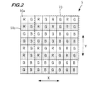
図2は、図1に示す固体撮像素子5の概略構成を示す平面模式図である。 FIG. 2 is a schematic plan view showing a schematic configuration of the solid-state imaging device 5 shown in FIG.
固体撮像素子5は、撮影光学系1の異なる瞳領域を通過する一対の光束の各々に対応する一対の像信号のうちの一方を得るための画素セル50aと、一対の像信号のうちの他方を得るための画素セル50bとを備える。以下では、画素セル50aと画素セル50bを区別しない場合、これらを画素セル50という。
The solid-state imaging device 5 includes a
画素セル50は、行方向Xとこれに直交する列方向Yに二次元状(図2の例では正方格子状)に配列されている。各画素セル50は、フォトダイオード等の光電変換部を含む。 The pixel cells 50 are arranged in a two-dimensional shape (in the example of FIG. 2, a square lattice shape) in the row direction X and the column direction Y orthogonal thereto. Each pixel cell 50 includes a photoelectric conversion unit such as a photodiode.
画素セル50の配置は、行方向Xに一定ピッチで並ぶ複数の画素セル50を含む画素セル行を、列方向Yに一定ピッチで複数個並べたものとなっている。 The arrangement of the pixel cells 50 is such that a plurality of pixel cell rows including a plurality of pixel cells 50 arranged at a constant pitch in the row direction X are arranged at a constant pitch in the column direction Y.
この配置において、奇数行にある画素セル行は、画素セル50aにより構成され、偶数行にある画素セル行は、画素セル50bにより構成されている。
In this arrangement, the pixel cell rows in the odd rows are constituted by the
画素セル50aと画素セル50bは、それぞれ、撮影光学系1の異なる瞳領域を通過する光束を受光するものである。つまり、奇数行にある画素セル50aによって、上記一対の像信号の一方を取得し、偶数行にある画素セル50bによって、上記一対の像信号の他方を取得できる。
The
画素セル50aは、赤色の波長域の光(R光)を検出する画素セル(R画素セル50aという)と、緑色の波長域の光(G光)を検出する画素セル(G画素セル50aという)と、青色の波長域の光(B光)を検出する画素セル(B画素セル50aという)の3種類の画素セルを含む。
The
画素セル50bは、R光を検出する画素セル(R画素セル50bという)と、G光を検出する画素セル(G画素セル50bという)と、B光を検出する画素セル(B画素セル50bという)の3種類の画素セルを含む。
The
図2では、R画素セル50a及びR画素セル50bには、ブロック内に“R”の文字を付している。また、G画素セル50a及びG画素セル50bには、ブロック内に“G”の文字を付している。また、B画素セル50a及びB画素セル50bには、ブロック内に“B”の文字を付している。
In FIG. 2, the letter “R” is added to the
図2に示すように、奇数行にある画素セル50aの検出色の並びはベイヤ状となっている。
As shown in FIG. 2, the arrangement of the detection colors of the
各画素セル50aに対して同一方向(列方向Y)の隣には、その画素セル50aと同じ種類の画素セル50bが配置されている。つまり、偶数行にある画素セル50bの検出色の並びもベイヤ状となっている。
A
列方向Yにおいて隣接する同一種類の画素セル50a及び画素セル50bにより、画素セルペアが構成される。固体撮像素子5は、この画素セルペアが正方格子状に配列されたものということもできる。
A pixel cell pair is constituted by the
図3は、図2に示す固体撮像素子5の点線で囲んだ部分70の詳細を示す模式図である。
FIG. 3 is a schematic diagram showing details of a
各画素セル50において中に“R”、“G”、又は“B”の文字が記入された領域は、遮光膜55に形成され光を受光する開口54であり、ハッチングを付した領域は遮光膜55による遮光領域である。
In each pixel cell 50, a region in which the letters “R”, “G”, or “B” are written is an
画素セル50aにおいては、開口54が行方向Xにおいて右側に偏心している。また、画素セル50bにおいては、開口54が行方向Xにおいて左側に偏心している。
In the
このように、ペア画素セルを構成する画素セル50aと画素セル50bは、開口54が行方向Xにおいて互いに逆方向にずれている。
As described above, the
この結果、固体撮像素子5を用いて被写体を撮影した場合、画素セル50aによって得られる第一の撮像画像信号は左眼で被写体を視たものとなり、画素セル50bによって得られる第二の撮像画像信号は右眼で被写体を視たものとなり、双方の撮像画像信号にはずれ量(位相差、視差)が生じる。
As a result, when the subject is photographed using the solid-state imaging device 5, the first captured image signal obtained by the
したがって、第一の撮像画像信号と第二の撮像画像信号を左右の撮像画像信号とすることで、単一の撮影光学系と単一の撮像素子で、立体画像の撮像が可能となる。 Therefore, by using the first captured image signal and the second captured image signal as the left and right captured image signals, it is possible to capture a stereoscopic image with a single imaging optical system and a single imaging element.
図1の3D画像生成部19は、固体撮像素子5から出力される第一の撮像画像信号から左眼用撮像画像データを生成し、固体撮像素子5から出力される第二の撮像画像信号から右眼用撮像画像データを生成し、これらを関連付けたものを、立体画像データとして生成する。
The 3D
図1のシステム制御部11は、固体撮像素子5から出力される第一の撮像画像信号と第二の撮像画像信号との位相差に基づいて、撮影光学系1の焦点調節を行う位相差AF制御を行う。
The system control unit 11 in FIG. 1 performs phase adjustment AF that adjusts the focus of the imaging
図1のデジタル信号処理部17は、固体撮像素子5から出力される第一の撮像画像信号及び第二の撮像画像信号のうち、画素セルペアから得られた撮像信号同士を加算する。これにより、被写体を単一の視点で撮影したものに相当する撮像画像信号を生成することができる。デジタル信号処理部17は、この撮像画像信号を処理することで、通常の二次元の撮像画像データを生成する。
The digital
このように、図1に示すデジタルカメラは、図2に示す構成の固体撮像素子5を搭載していることにより、立体画像の撮影と二次元画像の撮影の切り替えが容易となる。また、撮像用の固体撮像素子5を用いて位相差AFを行うことができるため、位相差AF専用のセンサを設けることなく、高速AFが可能になる。 As described above, since the digital camera shown in FIG. 1 is equipped with the solid-state imaging device 5 having the configuration shown in FIG. 2, it is easy to switch between capturing a stereoscopic image and capturing a two-dimensional image. Further, since the phase difference AF can be performed using the solid-state image pickup device 5 for imaging, high-speed AF is possible without providing a sensor dedicated to the phase difference AF.
本実施形態では、このような利点が得られる固体撮像素子5において、立体画像及び二次元画像の撮像画質低下や、位相差AFの精度低下を防ぐために、画素セル50の構成をその種類(検出色)毎に変更している。以下、詳述する。 In the present embodiment, in the solid-state imaging device 5 capable of obtaining such advantages, the configuration of the pixel cell 50 is determined according to the type (detection) in order to prevent deterioration in the imaging quality of the stereoscopic image and the two-dimensional image and the accuracy of the phase difference AF. The color is changed every time. Details will be described below.
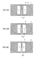
図4は、図2,3に示す固体撮像素子5におけるR画素セル50b、G画素セル50b、及びB画素セル50bの概略断面図である。FIG4AはR画素セル50bの断面図であり、FIG4BはG画素セル50bの断面図であり、FIG4CはB画素セル50bの断面図である。
4 is a schematic cross-sectional view of the
画素セル50aは、シリコン基板等の半導体基板53と、半導体基板53内に設けられた光電変換部(PD)54aと、光電変換部54a上に形成された絶縁層56と、絶縁層56上に形成されたカラーフィルタ57と、カラーフィルタ57上に形成されたマイクロレンズ58とを備える。
The
絶縁層56内には、光電変換部54aの光入射範囲を制限するための遮光膜55が形成されている。遮光膜55には光電変換部54a上方(光入射側)に開口54が形成されており、この開口54から、マイクロレンズ58によって集光された光が光電変換部54aに入射する。
A
画素セル50aにおいて、マイクロレンズ58の光軸と開口54の中心とは一致しておらず、開口54の中心がマイクロレンズ58の光軸に対し行方向Xにおいて左側に偏心した構成になっている。そして、開口54の偏心量は、画素セル50aの種類によって異なっている。
In the
具体的には、R画素セル50aの開口54の偏心量Orと、G画素セル50aの開口54の偏心量Ogと、B画素セル50aの開口54の偏心量Obとの関係が、Or>Og>Obとなっている。
Specifically, the relationship between the eccentricity Or of the
偏心量Orは、R画素セル50aにおけるマイクロレンズ58の光軸位置と開口54の中心位置との、行方向Xにおける距離を示す。
The eccentricity Or indicates the distance in the row direction X between the optical axis position of the
偏心量Ogは、G画素セル50aにおけるマイクロレンズ58の光軸位置と開口54の中心位置との、行方向Xにおける距離を示す。
The eccentric amount Og indicates the distance in the row direction X between the optical axis position of the
偏心量Obは、B画素セル50aにおけるマイクロレンズ58の光軸位置と開口54の中心位置との、行方向Xにおける距離を示す。
The eccentricity Ob represents the distance in the row direction X between the optical axis position of the
図5は、図4に示した各画素セル50aをマイクロレンズ58側から視た平面図である。図5ではマイクロレンズとカラーフィルタについては図示を省略している。
FIG. 5 is a plan view of each
FIG5AはFIG4Aに示すR画素セル50aの平面図を示し、FIG5BはFIG4Bに示すG画素セル50aの平面図を示し、FIG5CはFIG4Cに示すB画素セル50aの平面図を示す。
FIG. 5A shows a plan view of the
図4,5の例では、遮光膜55の開口54の左側端部の位置は各画素セル50aで同じとし、右側端部の行方向Xにおける位置を、長波長域の光を検出する画素セル50aほど、画素セル50aの光学中心(マイクロレンズ58の光軸位置)から離すことで、Or>Og>Obを実現している。
4 and 5, the position of the left end of the
前述したように、画素セル50aに入射する光束のスポット径は、画素セル50aの検出波長が長波長ほど大きくなるため、瞳分割性能(位相差分離量)は、検出波長が長波長になる画素セル50aほど低下する。そこで、図4,5に示すように、Or>Og>Obの関係を満たすようにすることで、各画素セル50aにおいて瞳分割性能を揃えることができる。
As described above, since the spot diameter of the light beam incident on the
したがって、画素セル50aの種類によって、位相差情報(撮影光学系1の異なる瞳領域を通過した一対の光束の各々に対応する像のずれ量)の取得精度にばらつきが生じず、位相差AFを精度よく行うことができる。また、立体画像データや二次元の撮像画像データ上で不自然な色付きが発生せず、撮像品質を高めることができる。
Therefore, there is no variation in the acquisition accuracy of the phase difference information (the amount of image shift corresponding to each of the pair of light beams that have passed through different pupil regions of the imaging optical system 1) depending on the type of the
なお、画素セル50bについては、図4,5に示した構成を左右反転させただけであるため、説明を省略する。
Note that the
以上の説明では、画素セル50において、その検出波長毎に遮光膜55の開口Kの大きさを変えている。しかし、瞳分割性能は、マイクロレンズ58の光軸から開口Kの中心までの距離によって決まるため、各画素セル50において開口Kの大きさは全て同じにしてもよい。
In the above description, in the pixel cell 50, the size of the opening K of the
例えば、図6に示すように、全ての画素セル50において開口54は同一形状とし、その開口54の中心位置を、画素セル50の種類に応じて変えた構成としてもよい。このように、開口Kを全ての画素セル50で同一形状にすることで、製造が容易になり、コスト削減に繋がる。
For example, as shown in FIG. 6, the
また、以上の説明では、Or>Og>Obとしたが、スポット光の大きさは、R画素セル50a,50bと、B画素セル50a,50bとの間で最も差が大きくなるため、少なくとも、Or>Obとなっていれば、位相差AF精度向上や画質向上の効果を得られる。
In the above description, Or> Og> Ob. However, since the spot light has the largest difference between the
例えば、図7に示すようにOr=Og>Obとしたり、図8に示すようにOr>Og=Obとしたりしてもよい。 For example, Or = Og> Ob as shown in FIG. 7 or Or> Og = Ob as shown in FIG.
図9は、図2に示す固体撮像素子5の変形例である固体撮像素子5aの平面模式図である。
FIG. 9 is a schematic plan view of a solid-
固体撮像素子5aは、図2における画素セル50aと画素セル50bとをそれぞれ45度回転させた上で、奇数行の画素セル行を、行方向Xにおける画素セル50の配列ピッチの1/2だけ行方向Xにずらした、所謂ハニカム配列としたものである。
The solid-
図10は、図9に示す固体撮像素子5aの領域Hの拡大図である。
FIG. 10 is an enlarged view of the region H of the solid-
図10に示すように、各画素セル50における遮光膜55の開口54の中心位置の、その各画素セル50の光軸中心からの離間距離は、R画素セル50a,50b>G画素セル50a,50b>B画素セル50a,50bとなっている。
As shown in FIG. 10, the distance from the center of the optical axis of each pixel cell 50 to the center position of the
このような画素セル配置でも、固体撮像素子5と同様の効果を得ることができる。 Even with such a pixel cell arrangement, the same effect as the solid-state imaging device 5 can be obtained.
図11は、図2に示す固体撮像素子5の変形例である固体撮像素子5bの構成を示す平面図である。
FIG. 11 is a plan view showing a configuration of a solid-
固体撮像素子5,5aは、撮影光学系1の異なる瞳領域を通過する一対の光束の両方を受光する画素セル(瞳分割されていない画素セル)を持たないものであった。これに対し、固体撮像素子5bは、瞳分割されていない画素セル50cと、これまで説明してきた瞳分割された画素セル50a,50bとを備えている。
The solid-
固体撮像素子5bでは、二次元状(図11の例では正方格子状)に配列された画素セル50cのうちの一部を、画素セル50a,50bとしている。図11では、R光を検出する画素セル50cとG光を検出する画素セル50cの一部を、画素セル50a,50bに置き換えている。
In the solid-
なお、R光を検出する画素セル50cとB光を検出する画素セル50cのそれぞれの一部を、画素セル50a,50bに置き換えた構成、G光を検出する画素セル50cとB光を検出する画素セル50cのそれぞれの一部を、画素セル50a,50bに置き換えた構成、R光を検出する画素セル50cとG光を検出する画素セル50cとB光を検出する画素セル50cのそれぞれの一部を、画素セル50a,50bに置き換えた構成としてもよい。
The
固体撮像素子5bが、瞳分割された画素セルとして、R光を検出する画素セル50a,50bと、G光を検出する画素セル50a,50bとのみを有する場合は、前述したOrとOgの関係はOr>Ogとなっていればよい。
When the solid-
固体撮像素子5bが、瞳分割された画素セルとして、R光を検出する画素セル50a,50bと、B光を検出する画素セル50a,50bとのみを有する場合は、前述したOrとObの関係はOr>Obとなっていればよい。
When the solid-
固体撮像素子5bが、瞳分割された画素セルとして、G光を検出する画素セル50a,50bと、B光を検出する画素セル50a,50bとのみを有する場合は、前述したOgとObの関係はOg>Obとなっていればよい。
When the solid-
固体撮像素子5bが、瞳分割された画素セルとして、R光を検出する画素セル50a,50bと、G光を検出する画素セル50a,50bと、B光を検出する画素セル50a,50bとを有する場合は、前述したOrとOgとObの関係はOr>Og>Og、Or=Og>Ob、Or>Og=Obのいずれかとなっていればよい。
The solid-
この固体撮像素子5bを搭載するデジタルカメラでは、画素セル50a,50bから取得した信号を用いて、システム制御部11が位相差AFを行う。具体的には、システム制御部11は、画素セル50aから取得した像信号と、画素セル50bから取得した像信号との位相差に基づいてAF制御を行う。
In a digital camera equipped with the solid-
このように、瞳分割されていない通常の画素セル50cが二次元状に配列された固体撮像素子において、その一部の画素セル50cを、瞳分割された画素セル50a,50bに置き換えたものであっても、Or,Og,Obの大小関係を上述したように設定することで、位相差AF精度の向上と撮像画像の品質向上を図ることができる。
In this way, in a solid-state imaging device in which
なお、固体撮像素子5bが、瞳分割された画素セルとして、R光を検出する画素セル50a,50bと、G光を検出する画素セル50a,50bと、B光を検出する画素セル50a,50bとを有するものとし、この3種類の画素セル50a,50bを全体に満遍なく配置しておくことで、3D撮影と2D撮影の両方に対応することが可能になる。
In addition, the
例えば、3D撮影時には、3種類の画素セル50a,50bから取得した撮像画像信号を用いて立体画像データを生成し、2D撮影時には、画素セル50cから取得した撮像画像信号を用いて撮像画像データを生成するといった使い方が可能である。なお、2D撮影時には、画素セル50a,50bに対応する信号については、画素セル50cから得た信号を用いて補間生成すればよい。
For example, in 3D shooting, stereoscopic image data is generated using captured image signals acquired from three types of
図12は、図2に示す固体撮像素子5の変形例である固体撮像素子5cの構成を示す平面図である。
FIG. 12 is a plan view showing a configuration of a solid-
固体撮像素子5cは、画素セル50aと画素セル50bが二次元状に配列された点では固体撮像素子5と同じである。固体撮像素子5cは、奇数列に画素セル50aがベイヤ状に配列され、各画素セル50aに対し行方向Xの隣に、その各画素セル50aと同一色の光を検出する画素セル50bが配置された構成である。固体撮像素子5cでは、行方向Xにおいて隣接する同一種類の画素セル50a及び画素セル50bにより、画素セルペアが構成される。
The solid-state
図13は、図12に示す固体撮像素子5cにおけるR光を検出する画素セルペア、G光を検出する画素セルペア、B光を検出する画素セルペアの詳細を示す図である。
FIG. 13 is a diagram showing details of a pixel cell pair for detecting R light, a pixel cell pair for detecting G light, and a pixel cell pair for detecting B light in the solid-
FIG13Aは、固体撮像素子5cにおけるR光を検出する画素セルペアの構成を示す。FIG13Bは、固体撮像素子5cにおけるG光を検出する画素セルペアの構成を示す。FIG13Cは、固体撮像素子5cにおけるB光を検出する画素セルペアの構成を示す。
FIG. 13A shows the configuration of a pixel cell pair that detects R light in the solid-
図13に示すように、固体撮像素子5cでは、画素セルペアに対して1つのマイクロレンズ53aが設けられている。マイクロレンズ53aは、画素セルペアを構成する2つの画素セル50に跨って設けられた楕円形状となっている。
As shown in FIG. 13, in the solid-
この固体撮像素子5cにおいても、マイクロレンズ53aの光軸と、そのマイクロレンズ53aに対応する各画素セル50の開口54の中心との距離をOr,Og,Obとして、これらの距離が上述してきたような関係となっている。
Also in this solid-
このように、画素セルペアに対して1つのマイクロレンズを設ける構成であっても、固体撮像素子5と同様の効果を得ることができる。 Thus, even if it is the structure which provides one microlens with respect to a pixel cell pair, the effect similar to the solid-state image sensor 5 can be acquired.
次に、撮像装置としてスマートフォンの構成について説明する。 Next, the configuration of a smartphone as an imaging device will be described.
図14は、本発明の撮影装置の一実施形態であるスマートフォン200の外観を示すものである。図14に示すスマートフォン200は、平板状の筐体201を有し、筐体201の一方の面に表示部としての表示パネル202と、入力部としての操作パネル203とが一体となった表示入力部204を備えている。また、このような筐体201は、スピーカ205と、マイクロホン206と、操作部207と、カメラ部208とを備えている。なお、筐体201の構成はこれに限定されず、例えば、表示部と入力部とが独立した構成を採用したり、折り畳み構造やスライド機構を有する構成を採用したりすることもできる。
FIG. 14 shows an appearance of a
図15は、図14に示すスマートフォン200の構成を示すブロック図である。図14に示すように、スマートフォンの主たる構成要素として、無線通信部210と、表示入力部204と、通話部211と、操作部207と、カメラ部208と、記憶部212と、外部入出力部213と、GPS(Global Positioning System)受信部214と、モーションセンサ部215と、電源部216と、主制御部220とを備える。また、スマートフォン200の主たる機能として、図示省略の基地局装置BSと図示省略の移動通信網NWとを介した移動無線通信を行う無線通信機能を備える。
FIG. 15 is a block diagram showing a configuration of the
無線通信部210は、主制御部220の指示にしたがって、移動通信網NWに収容された基地局装置BSに対し無線通信を行うものである。この無線通信を使用して、音声データ、画像データ等の各種ファイルデータ、電子メールデータなどの送受信や、Webデータやストリーミングデータなどの受信を行う。
The
表示入力部204は、主制御部220の制御により、画像(静止画像及び動画像)や文字情報などを表示して視覚的にユーザに情報を伝達するとともに、表示した情報に対するユーザ操作を検出する、いわゆるタッチパネルであって、表示パネル202と、操作パネル203とを備える。
The
表示パネル202は、LCD(Liquid Crystal Display)、OELD(Organic Electro−Luminescence Display)などを表示デバイスとして用いたものである。
The
操作パネル203は、表示パネル202の表示面上に表示される画像を視認可能に載置され、ユーザの指や尖筆によって操作される一又は複数の座標を検出するデバイスである。このデバイスをユーザの指や尖筆によって操作すると、操作に起因して発生する検出信号を主制御部220に出力する。次いで、主制御部220は、受信した検出信号に基づいて、表示パネル202上の操作位置(座標)を検出する。
The
図14に示すように、本発明の撮影装置の一実施形態として例示しているスマートフォン200の表示パネル202と操作パネル203とは一体となって表示入力部204を構成しているが、操作パネル203が表示パネル202を完全に覆うような配置となっている。
As shown in FIG. 14, the
係る配置を採用した場合、操作パネル203は、表示パネル202外の領域についても、ユーザ操作を検出する機能を備えてもよい。換言すると、操作パネル203は、表示パネル202に重なる重畳部分についての検出領域(以下、表示領域と称する)と、それ以外の表示パネル202に重ならない外縁部分についての検出領域(以下、非表示領域と称する)とを備えていてもよい。
When such an arrangement is adopted, the
なお、表示領域の大きさと表示パネル202の大きさとを完全に一致させても良いが、両者を必ずしも一致させる必要はない。また、操作パネル203が、外縁部分と、それ以外の内側部分の2つの感応領域を備えていてもよい。更に、外縁部分の幅は、筐体201の大きさなどに応じて適宜設計されるものである。更にまた、操作パネル203で採用される位置検出方式としては、マトリクススイッチ方式、抵抗膜方式、表面弾性波方式、赤外線方式、電磁誘導方式、静電容量方式などが挙げられ、いずれの方式を採用することもできる。
Note that the size of the display area and the size of the
通話部211は、スピーカ205やマイクロホン206を備え、マイクロホン206を通じて入力されたユーザの音声を主制御部220にて処理可能な音声データに変換して主制御部220に出力したり、無線通信部210或いは外部入出力部213により受信された音声データを復号してスピーカ205から出力させたりするものである。また、図14に示すように、例えば、スピーカ205を表示入力部204が設けられた面と同じ面に搭載し、マイクロホン206を筐体201の側面に搭載することができる。
The
操作部207は、キースイッチなどを用いたハードウェアキーであって、ユーザからの指示を受け付けるものである。例えば、図14に示すように、操作部207は、スマートフォン200の筐体201の側面に搭載され、指などで押下されるとオンとなり、指を離すとバネなどの復元力によってオフ状態となる押しボタン式のスイッチである。
The
記憶部212は、主制御部220の制御プログラムや制御データ、アプリケーションソフトウェア、通信相手の名称や電話番号などを対応づけたアドレスデータ、送受信した電子メールのデータ、WebブラウジングによりダウンロードしたWebデータや、ダウンロードしたコンテンツデータを記憶し、またストリーミングデータなどを一時的に記憶するものである。また、記憶部212は、スマートフォン内蔵の内部記憶部217と着脱自在な外部メモリスロットを有する外部記憶部218により構成される。なお、記憶部212を構成するそれぞれの内部記憶部217と外部記憶部218は、フラッシュメモリタイプ(flash memory type)、ハードディスクタイプ(hard disk type)、マルチメディアカードマイクロタイプ(multimedia card micro type)、カードタイプのメモリ(例えば、MicroSD(登録商標)メモリ等)、RAM(Random Access Memory)、ROM(Read Only Memory)などの格納媒体を用いて実現される。
The
外部入出力部213は、スマートフォン200に連結される全ての外部機器とのインターフェースの役割を果たすものであり、他の外部機器に通信等(例えば、ユニバーサルシリアルバス(USB)、IEEE1394など)又はネットワーク(例えば、インターネット、無線LAN、ブルートゥース(Bluetooth)(登録商標)、RFID(Radio Frequency Identification)、赤外線通信(Infrared Data Association:IrDA)(登録商標)、UWB(Ultra Wideband)(登録商標)、ジグビー(ZigBee)(登録商標)など)により直接的又は間接的に接続するためのものである。
The external input /
スマートフォン200に連結される外部機器としては、例えば、有/無線ヘッドセット、有/無線外部充電器、有/無線データポート、カードソケットを介して接続されるメモリカード(Memory card)やSIM(Subscriber Identity Module Card)/UIM(User Identity Module Card)カード、オーディオ・ビデオI/O(Input/Output)端子を介して接続される外部オーディオ・ビデオ機器、無線接続される外部オーディオ・ビデオ機器、有/無線接続されるスマートフォン、有/無線接続されるパーソナルコンピュータ、有/無線接続されるPDA、有/無線接続されるパーソナルコンピュータ、イヤホンなどがある。外部入出力部213は、このような外部機器から伝送を受けたデータをスマートフォン200の内部の各構成要素に伝達することや、スマートフォン200の内部のデータが外部機器に伝送されるようにすることができる。
As an external device connected to the
GPS受信部214は、主制御部220の指示にしたがって、GPS衛星ST1〜STnから送信されるGPS信号を受信し、受信した複数のGPS信号に基づく測位演算処理を実行し、そのスマートフォン200の緯度、経度、高度を含む位置情報を検出する。GPS受信部214は、無線通信部210や外部入出力部213(例えば、無線LAN)から位置情報を取得できる時には、その位置情報を用いて位置を検出することもできる。
The
モーションセンサ部215は、例えば、3軸の加速度センサなどを備え、主制御部220の指示にしたがって、スマートフォン200の物理的な動きを検出する。スマートフォン200の物理的な動きを検出することにより、スマートフォン200の動く方向や加速度が検出される。係る検出結果は、主制御部220に出力されるものである。
The
電源部216は、主制御部220の指示にしたがって、スマートフォン200の各部に、バッテリ(図示しない)に蓄えられる電力を供給するものである。
The
主制御部220は、マイクロプロセッサを備え、記憶部212が記憶する制御プログラムや制御データにしたがって動作し、スマートフォン200の各部を統括して制御するものである。また、主制御部220は、無線通信部210を通じて、音声通信やデータ通信を行うために、通信系の各部を制御する移動通信制御機能と、アプリケーション処理機能を備える。
The
アプリケーション処理機能は、記憶部212が記憶するアプリケーションソフトウェアにしたがって主制御部220が動作することにより実現するものである。アプリケーション処理機能としては、例えば、外部入出力部213を制御して対向機器とデータ通信を行う赤外線通信機能や、電子メールの送受信を行う電子メール機能、Webページを閲覧するWebブラウジング機能などがある。
The application processing function is realized by the
また、主制御部220は、受信データやダウンロードしたストリーミングデータなどの画像データ(静止画像や動画像のデータ)に基づいて、映像を表示入力部204に表示する等の画像処理機能を備える。画像処理機能とは、主制御部220が、上記画像データを復号し、この復号結果に画像処理を施して、画像を表示入力部204に表示する機能のことをいう。
Further, the
更に、主制御部220は、表示パネル202に対する表示制御と、操作部207、操作パネル203を通じたユーザ操作を検出する操作検出制御を実行する。表示制御の実行により、主制御部220は、アプリケーションソフトウェアを起動するためのアイコンや、スクロールバー(繋がった状態で連続的に表示させる指示を行うためのもの)などのソフトウェアキーを表示したり、或いは電子メールを作成したりするためのウィンドウを表示する。なお、スクロールバーとは、表示パネル202の表示領域に収まりきれない大きな画像などについて、画像の表示部分を移動する指示を受け付けるためのソフトウェアキーのことをいう。
Further, the
また、操作検出制御の実行により、主制御部220は、操作部207を通じたユーザ操作を検出したり、操作パネル203を通じて、上記アイコンに対する操作や、上記ウィンドウの入力欄に対する文字列の入力を受け付けたり、或いは、スクロールバーを通じた表示画像のスクロール要求を受け付ける。
In addition, by executing the operation detection control, the
更に、操作検出制御の実行により主制御部220は、操作パネル203に対する操作位置が、表示パネル202に重なる重畳部分(表示領域)か、それ以外の表示パネル202に重ならない外縁部分(非表示領域)かを判定し、操作パネル203の感応領域や、ソフトウェアキーの表示位置を制御するタッチパネル制御機能を備える。
Further, by executing the operation detection control, the
また、主制御部220は、操作パネル203に対するジェスチャ操作を検出し、検出したジェスチャ操作に応じて、予め設定された機能を実行することもできる。ジェスチャ操作とは、従来の単純なタッチ操作ではなく、指などによって軌跡を描いたり、複数の位置を同時に指定したり、或いはこれらを組み合わせて、複数の位置から少なくとも1つについて軌跡を描く操作を意味する。
The
カメラ部208は、図1に示したデジタルカメラにおける外部メモリ制御部20、記録媒体21、表示制御部22、表示部23、及び操作部14以外の構成を含む。カメラ部208によって生成された撮像画像データは、記憶部212に記録したり、外部入出力部213や無線通信部210を通じて出力したりすることができる。図14に示すにスマートフォン200において、カメラ部208は表示入力部204と同じ面に搭載されているが、カメラ部208の搭載位置はこれに限らず、表示入力部204の背面に搭載されてもよい。
The
また、カメラ部208はスマートフォン200の各種機能に利用することができる。例えば、表示パネル202にカメラ部208で取得した画像を表示することや、操作パネル203の操作入力のひとつとして、カメラ部208の画像を利用することができる。また、GPS受信部214が位置を検出する際に、カメラ部208からの画像を参照して位置を検出することもできる。更には、カメラ部208からの画像を参照して、3軸の加速度センサを用いずに、或いは、3軸の加速度センサと併用して、スマートフォン200のカメラ部208の光軸方向を判断することや、現在の使用環境を判断することもできる。勿論、カメラ部208からの画像をアプリケーションソフトウェア内で利用することもできる。
The
その他、静止画又は動画の画像データにGPS受信部214により取得した位置情報、マイクロホン206により取得した音声情報(主制御部等により、音声テキスト変換を行ってテキスト情報となっていてもよい)、モーションセンサ部215により取得した姿勢情報等などを付加して記憶部212に記録したり、外部入出力部213や無線通信部210を通じて出力したりすることもできる。
In addition, the position information acquired by the
以上のような構成のスマートフォン200においても、カメラ部208の撮像素子として固体撮像素子5,5a,5bを用いることで、高精度の位相差AF,高品質の撮影が可能になる。
Even in the
以上説明してきたように、本明細書には以下の事項が開示されている。 As described above, the following items are disclosed in this specification.
開示された撮像素子は、撮影光学系の異なる瞳領域を通過する一対の光束の各々に対応する一対の像信号を出力可能な撮像素子であって、光電変換部、上記光電変換部の光入射側に設けられ上記光電変換部に光を集光するマイクロレンズ、及び上記光電変換部と上記マイクロレンズとの間に設けられ、上記光電変換部の光入射側に開口を有する遮光膜、を含む画素セルを有し、上記画素セルは、上記マイクロレンズの光軸に対して上記遮光膜の開口の中心位置が互いに逆方向に偏心された第一の画素セル及び第二の画素セルを有するペアを複数組含み、上記第一の画素セルと上記第二の画素セルは、それぞれ、異なる波長域の光を検出する複数種類に分けられており、上記画素セルにおいて、上記光電変換部により検出される光の波長域が最も長波長側となる上記第一の画素セル及び上記第二の画素セルのそれぞれに対する上記マイクロレンズの光軸から上記遮光膜の開口中心までの距離が、上記光の波長域が最も短波長側となる上記第一の画素セル及び上記第二の画素セルのそれぞれに対する上記距離よりも長いものである。 The disclosed imaging device is an imaging device capable of outputting a pair of image signals corresponding to each of a pair of light beams passing through different pupil regions of a photographing optical system, and includes a photoelectric conversion unit and light incidence of the photoelectric conversion unit And a light-shielding film provided between the photoelectric conversion unit and the microlens and having an opening on the light incident side of the photoelectric conversion unit. A pair having a first pixel cell and a second pixel cell in which the center position of the opening of the light-shielding film is decentered in opposite directions with respect to the optical axis of the microlens. The first pixel cell and the second pixel cell are divided into a plurality of types that detect light in different wavelength ranges, and are detected by the photoelectric conversion unit in the pixel cell. The wavelength range of light The distance from the optical axis of the microlens to the opening center of the light shielding film for each of the first pixel cell and the second pixel cell on the long wavelength side is the shortest wavelength side of the light wavelength region. Longer than the distance to each of the first pixel cell and the second pixel cell.
開示された撮像素子は、上記複数種類の画素セルは、赤色光を検出する画素セル、青色光を検出する画素セル、及び緑色光を検出する画素セルのうちの少なくとも2つを含むものである。 In the disclosed imaging device, the plurality of types of pixel cells include at least two of a pixel cell that detects red light, a pixel cell that detects blue light, and a pixel cell that detects green light.
開示された撮像素子は、(上記赤色光を検出する画素セルにおける上記距離)>(上記緑色光を検出する画素セルにおける上記距離)>(上記青色光を検出する画素セルにおける上記距離)となっているものである。 The disclosed imaging element is (the distance in the pixel cell that detects the red light)> (the distance in the pixel cell that detects the green light)> (the distance in the pixel cell that detects the blue light). It is what.
開示された撮像素子は、上記赤色光を検出する画素セルと上記青色光を検出する画素セルと上記緑色光を検出する画素セルのうちの2つについては、上記距離が同じであるものを含む。 The disclosed imaging device includes the pixel cell that detects the red light, the pixel cell that detects the blue light, and the pixel cell that detects the green light that have the same distance. .
開示された撮像素子は、上記赤色光を検出する画素セルと上記緑色光を検出する画素セルについては、上記距離が同じであり、上記青色光を検出する画素セルについては、上記距離が、上記赤色光を検出する画素セル及び上記緑色光を検出する画素セルにおける上記距離よりも短いものである。 In the disclosed imaging device, the pixel cell that detects the red light and the pixel cell that detects the green light have the same distance, and the pixel cell that detects the blue light has the distance It is shorter than the distance in the pixel cell for detecting red light and the pixel cell for detecting green light.
開示された撮像素子は、上記青色光を検出する画素セルと上記緑色光を検出する画素セルについては、上記距離が同じであり、上記赤色光を検出する画素セルについては、上記距離が、上記青色光を検出する画素セル及び上記緑色光を検出する画素セルにおける上記距離よりも長いものである。 In the disclosed imaging device, the pixel cell detecting the blue light and the pixel cell detecting the green light have the same distance, and the pixel cell detecting the red light has the distance It is longer than the distance in the pixel cell that detects blue light and the pixel cell that detects green light.
開示された撮像素子は、上記少なくとも4つの画素セルにおける上記遮光膜の開口は同一形状となっているものである。 In the disclosed imaging device, the openings of the light shielding film in the at least four pixel cells have the same shape.
開示された撮像素子は、上記ペアは、上記第一の画素セルと、その第一の画素セルに隣接して配置され、その第一の画素セルと同じ波長域の光を検出する上記第二の画素セルとを有して構成され、上記ペアが二次元状に配列されているものである。 In the disclosed imaging device, the pair is disposed adjacent to the first pixel cell and the first pixel cell, and detects the light in the same wavelength region as the first pixel cell. And the above-mentioned pairs are two-dimensionally arranged.
開示された撮像装置は、上記撮像素子を備えるものである。 The disclosed imaging device includes the imaging device.
開示された撮像装置は、上記複数組のペアから得られる信号を用いて立体画像データを生成する立体画像生成部を備えるものである。 The disclosed imaging apparatus includes a stereoscopic image generation unit that generates stereoscopic image data using signals obtained from the plurality of pairs.
開示された撮像装置は、上記複数組のペアから得られる信号を用いて焦点調節を行う焦点調節部を備えるものである。 The disclosed imaging apparatus includes a focus adjustment unit that performs focus adjustment using signals obtained from the plurality of pairs.
本発明に係る撮像素子及び撮像装置は、撮影光学系の異なる瞳領域を通過した一対の光束の各々に対応する像のずれ量を精度良く検出でき、位相差AFの精度向上や撮像画像上の不自然な色付きの防止を図ることが可能となり、撮像品質を向上させることができる。そのため、この撮像素子及び撮像装置はデジタルカメラやスマートフォン等の各種情報機器に用いると有用である。
本出願は、2012年3月28日出願の日本特許出願(特願2012−74309)に基づくものであり、その内容はここに参照として取り込まれる。The image pickup device and the image pickup apparatus according to the present invention can accurately detect the shift amount of an image corresponding to each of a pair of light beams that have passed through different pupil regions of the photographing optical system. It is possible to prevent unnatural coloring and improve imaging quality. For this reason, the imaging device and the imaging device are useful when used in various information devices such as a digital camera and a smartphone.
This application is based on a Japanese patent application filed on Mar. 28, 2012 (Japanese Patent Application No. 2012-74309), the contents of which are incorporated herein by reference.
5 固体撮像素子
50a,50b 画素セル
54 遮光膜開口
Og 遮光膜開口の偏心量5 Solid-
Claims (11)
光電変換部、前記光電変換部の光入射側に設けられ前記光電変換部に光を集光するマイクロレンズ、及び前記光電変換部と前記マイクロレンズとの間に設けられ、前記光電変換部の光入射側に開口を有する遮光膜、を含む画素セルを有し、
前記画素セルは、前記マイクロレンズの光軸に対して前記遮光膜の開口の中心位置が互いに逆方向に偏心された第一の画素セル及び第二の画素セルを有するペアを複数組含み、
前記第一の画素セルと前記第二の画素セルは、それぞれ、異なる波長域の光を検出する複数種類に分けられており、
前記画素セルにおいて、前記光電変換部により検出される光の波長域が最も長波長側となる前記第一の画素セル及び前記第二の画素セルのそれぞれに対する前記マイクロレンズの光軸から前記遮光膜の開口中心までの距離が、前記光の波長域が最も短波長側となる前記第一の画素セル及び前記第二の画素セルのそれぞれに対する前記距離よりも長い撮像素子。An imaging device capable of outputting a pair of image signals corresponding to each of a pair of light beams that pass through different pupil regions of the photographing optical system,
A photoelectric conversion unit, a microlens provided on a light incident side of the photoelectric conversion unit and condensing light on the photoelectric conversion unit, and provided between the photoelectric conversion unit and the microlens, and the light of the photoelectric conversion unit A pixel cell including a light-shielding film having an opening on the incident side;
The pixel cell includes a plurality of pairs each having a first pixel cell and a second pixel cell in which the center position of the opening of the light shielding film is decentered in opposite directions with respect to the optical axis of the microlens,
The first pixel cell and the second pixel cell are each divided into a plurality of types that detect light in different wavelength ranges,
In the pixel cell, the light-shielding film from the optical axis of the microlens for each of the first pixel cell and the second pixel cell in which the wavelength range of light detected by the photoelectric conversion unit is the longest wavelength side An image sensor in which the distance to the center of the aperture is longer than the distance to each of the first pixel cell and the second pixel cell in which the wavelength range of the light is the shortest wavelength side.
前記複数種類の画素セルは、赤色光を検出する画素セル、青色光を検出する画素セル、及び緑色光を検出する画素セルのうちの少なくとも2つを含む撮像素子。The imaging device according to claim 1,
The plurality of types of pixel cells may include at least two of a pixel cell that detects red light, a pixel cell that detects blue light, and a pixel cell that detects green light.
(前記赤色光を検出する画素セルにおける前記距離)>(前記緑色光を検出する画素セルにおける前記距離)>(前記青色光を検出する画素セルにおける前記距離)となっている撮像素子。The imaging device according to claim 2,
(The distance in the pixel cell that detects the red light)> (The distance in the pixel cell that detects the green light)> (The distance in the pixel cell that detects the blue light).
前記赤色光を検出する画素セルと前記青色光を検出する画素セルと前記緑色光を検出する画素セルのうちの2つについては、前記距離が同じである撮像素子。The imaging device according to claim 2,
An imaging device in which the distance is the same for two of the pixel cell that detects the red light, the pixel cell that detects the blue light, and the pixel cell that detects the green light.
前記赤色光を検出する画素セルと前記緑色光を検出する画素セルについては、前記距離が同じであり、
前記青色光を検出する画素セルについては、前記距離が、前記赤色光を検出する画素セル及び前記緑色光を検出する画素セルにおける前記距離よりも短い撮像素子。The imaging device according to claim 4,
For the pixel cell that detects the red light and the pixel cell that detects the green light, the distance is the same,
As for the pixel cell that detects the blue light, the distance is shorter than the distance between the pixel cell that detects the red light and the pixel cell that detects the green light.
前記青色光を検出する画素セルと前記緑色光を検出する画素セルについては、前記距離が同じであり、
前記赤色光を検出する画素セルについては、前記距離が、前記青色光を検出する画素セル及び前記緑色光を検出する画素セルにおける前記距離よりも長い撮像素子。The imaging device according to claim 4,
For the pixel cell that detects the blue light and the pixel cell that detects the green light, the distance is the same,
For the pixel cell that detects the red light, the distance is longer than the distance in the pixel cell that detects the blue light and the pixel cell that detects the green light.
前記少なくとも4つの画素セルにおける前記遮光膜の開口は同一形状となっている撮像素子。The imaging device according to any one of claims 1 to 6,
An image sensor in which openings of the light shielding film in the at least four pixel cells have the same shape.
前記ペアは、前記第一の画素セルと、当該第一の画素セルに隣接して配置され当該第一の画素セルと同じ波長域の光を検出する前記第二の画素セルとを有して構成され、
前記ペアが二次元状に配列されている撮像素子。The imaging device according to any one of claims 1 to 6,
The pair includes the first pixel cell and the second pixel cell that is arranged adjacent to the first pixel cell and detects light in the same wavelength region as the first pixel cell. Configured,
An image sensor in which the pairs are arranged two-dimensionally.
前記複数組のペアから得られる信号を用いて立体画像データを生成する立体画像生成部を備える撮像装置。The imaging device according to claim 9,
An imaging apparatus including a stereoscopic image generation unit that generates stereoscopic image data using signals obtained from the plurality of pairs.
前記複数組のペアから得られる信号を用いて焦点調節を行う焦点調節部を備える撮像装置。The imaging apparatus according to claim 9 or 10,
An imaging apparatus comprising a focus adjustment unit that performs focus adjustment using signals obtained from the plurality of pairs.
Priority Applications (1)
| Application Number | Priority Date | Filing Date | Title |
|---|---|---|---|
| JP2014507464A JP5542248B2 (en) | 2012-03-28 | 2013-01-23 | Imaging device and imaging apparatus |
Applications Claiming Priority (4)
| Application Number | Priority Date | Filing Date | Title |
|---|---|---|---|
| JP2012074309 | 2012-03-28 | ||
| JP2012074309 | 2012-03-28 | ||
| PCT/JP2013/051283 WO2013145821A1 (en) | 2012-03-28 | 2013-01-23 | Imaging element and imaging device |
| JP2014507464A JP5542248B2 (en) | 2012-03-28 | 2013-01-23 | Imaging device and imaging apparatus |
Publications (2)
| Publication Number | Publication Date |
|---|---|
| JP5542248B2 true JP5542248B2 (en) | 2014-07-09 |
| JPWO2013145821A1 JPWO2013145821A1 (en) | 2015-12-10 |
Family
ID=49259107
Family Applications (1)
| Application Number | Title | Priority Date | Filing Date |
|---|---|---|---|
| JP2014507464A Expired - Fee Related JP5542248B2 (en) | 2012-03-28 | 2013-01-23 | Imaging device and imaging apparatus |
Country Status (5)
| Country | Link |
|---|---|
| US (1) | US9204114B2 (en) |
| EP (1) | EP2833406B1 (en) |
| JP (1) | JP5542248B2 (en) |
| CN (1) | CN104221149B (en) |
| WO (1) | WO2013145821A1 (en) |
Families Citing this family (6)
| Publication number | Priority date | Publication date | Assignee | Title |
|---|---|---|---|---|
| CN106200882B (en) * | 2015-04-30 | 2019-05-10 | 原相科技股份有限公司 | Sensing element and optical ranging system |
| CN110598685B (en) * | 2015-09-14 | 2023-06-30 | 原相科技股份有限公司 | Imaging device for resolving foreground |
| JP2017157804A (en) * | 2016-03-04 | 2017-09-07 | キヤノン株式会社 | Imaging apparatus |
| DE102016212778A1 (en) * | 2016-07-13 | 2018-01-18 | Robert Bosch Gmbh | Image sensor for a camera |
| US10270947B2 (en) * | 2016-09-15 | 2019-04-23 | Microsoft Technology Licensing, Llc | Flat digital image sensor |
| KR20180033003A (en) | 2016-09-23 | 2018-04-02 | 삼성전자주식회사 | Method and electrionic device for detecting wavelength spectrum of incident light |
Citations (3)
| Publication number | Priority date | Publication date | Assignee | Title |
|---|---|---|---|---|
| JP2007281296A (en) * | 2006-04-10 | 2007-10-25 | Nikon Corp | Solid imaging devise and electronic camera |
| JP2009089144A (en) * | 2007-10-01 | 2009-04-23 | Nikon Corp | Electronic camera |
| JP2010093757A (en) * | 2008-10-10 | 2010-04-22 | Canon Inc | Imaging device, method of controlling the same, and program |
Family Cites Families (12)
| Publication number | Priority date | Publication date | Assignee | Title |
|---|---|---|---|---|
| JP2005086186A (en) * | 2003-09-11 | 2005-03-31 | Matsushita Electric Ind Co Ltd | Solid state imaging apparatus and manufacturing method therefor |
| US7274011B2 (en) * | 2004-12-27 | 2007-09-25 | Teledyne Licensing, Llc | Spectral imager and fabrication method |
| DE102006047941B4 (en) * | 2006-10-10 | 2008-10-23 | Fraunhofer-Gesellschaft zur Förderung der angewandten Forschung e.V. | Device for homogenizing radiation with non-regular microlens arrays |
| KR100825805B1 (en) * | 2007-02-13 | 2008-04-29 | 삼성전자주식회사 | Image sensor device and method of fabricating the same sensor device |
| US7898738B2 (en) * | 2007-09-10 | 2011-03-01 | Oki Data Corporation | Lens array, manufacturing method thereof, LED head having lens array, exposure device having LED head, image forming apparatus having exposure device, and reading apparatus |
| WO2009087974A1 (en) * | 2008-01-11 | 2009-07-16 | Panasonic Corporation | Binocular camera module |
| US8748799B2 (en) * | 2010-12-14 | 2014-06-10 | Zena Technologies, Inc. | Full color single pixel including doublet or quadruplet si nanowires for image sensors |
| JP2010093081A (en) * | 2008-10-08 | 2010-04-22 | Panasonic Corp | Solid-state imaging device and method for manufacturing the same |
| US8558940B2 (en) * | 2008-11-27 | 2013-10-15 | Nikon Corporation | Image sensor and image-capturing device |
| JP5278123B2 (en) | 2009-04-06 | 2013-09-04 | 株式会社ニコン | Imaging device |
| JP5159700B2 (en) * | 2009-05-19 | 2013-03-06 | キヤノン株式会社 | Optical apparatus and focus detection method |
| WO2011148574A1 (en) * | 2010-05-28 | 2011-12-01 | パナソニック株式会社 | Solid-state image pickup device |
-
2013
- 2013-01-23 EP EP13769765.2A patent/EP2833406B1/en not_active Not-in-force
- 2013-01-23 WO PCT/JP2013/051283 patent/WO2013145821A1/en active Application Filing
- 2013-01-23 CN CN201380017557.XA patent/CN104221149B/en active Active
- 2013-01-23 JP JP2014507464A patent/JP5542248B2/en not_active Expired - Fee Related
-
2014
- 2014-09-26 US US14/498,558 patent/US9204114B2/en active Active
Patent Citations (3)
| Publication number | Priority date | Publication date | Assignee | Title |
|---|---|---|---|---|
| JP2007281296A (en) * | 2006-04-10 | 2007-10-25 | Nikon Corp | Solid imaging devise and electronic camera |
| JP2009089144A (en) * | 2007-10-01 | 2009-04-23 | Nikon Corp | Electronic camera |
| JP2010093757A (en) * | 2008-10-10 | 2010-04-22 | Canon Inc | Imaging device, method of controlling the same, and program |
Also Published As
| Publication number | Publication date |
|---|---|
| CN104221149A (en) | 2014-12-17 |
| US9204114B2 (en) | 2015-12-01 |
| CN104221149B (en) | 2016-08-24 |
| EP2833406A4 (en) | 2015-10-28 |
| US20150009373A1 (en) | 2015-01-08 |
| JPWO2013145821A1 (en) | 2015-12-10 |
| WO2013145821A1 (en) | 2013-10-03 |
| EP2833406B1 (en) | 2016-10-26 |
| EP2833406A1 (en) | 2015-02-04 |
Similar Documents
| Publication | Publication Date | Title |
|---|---|---|
| JP5542249B2 (en) | Image pickup device, image pickup apparatus using the same, and image pickup method | |
| JP5775976B2 (en) | Imaging apparatus, defocus amount calculation method, and imaging optical system | |
| JP5690977B2 (en) | Imaging device and imaging apparatus | |
| JP5690974B2 (en) | Imaging apparatus and focus control method | |
| JP6031587B2 (en) | Imaging apparatus, signal processing method, and signal processing program | |
| JP5799178B2 (en) | Imaging apparatus and focus control method | |
| EP2961153B1 (en) | Image pickup device | |
| JP6165680B2 (en) | Imaging device | |
| JP5982601B2 (en) | Imaging apparatus and focus control method | |
| JP5779726B2 (en) | Imaging apparatus and exposure determination method | |
| JP5750550B2 (en) | Imaging apparatus and focus control method | |
| JP5542248B2 (en) | Imaging device and imaging apparatus | |
| CN110447223B (en) | Image pickup apparatus | |
| JP5747124B2 (en) | Imaging device | |
| JP5677628B2 (en) | Imaging apparatus and imaging method | |
| WO2014065004A1 (en) | Imaging device and focus control method therefor | |
| JP2013211790A (en) | Imaging apparatus | |
| WO2013145887A1 (en) | Imaging device and imaging method |
Legal Events
| Date | Code | Title | Description |
|---|---|---|---|
| A975 | Report on accelerated examination |
Free format text: JAPANESE INTERMEDIATE CODE: A971005 Effective date: 20140403 |
|
| TRDD | Decision of grant or rejection written | ||
| A01 | Written decision to grant a patent or to grant a registration (utility model) |
Free format text: JAPANESE INTERMEDIATE CODE: A01 Effective date: 20140408 |
|
| A61 | First payment of annual fees (during grant procedure) |
Free format text: JAPANESE INTERMEDIATE CODE: A61 Effective date: 20140502 |
|
| R150 | Certificate of patent or registration of utility model |
Ref document number: 5542248 Country of ref document: JP Free format text: JAPANESE INTERMEDIATE CODE: R150 |
|
| R250 | Receipt of annual fees |
Free format text: JAPANESE INTERMEDIATE CODE: R250 |
|
| R250 | Receipt of annual fees |
Free format text: JAPANESE INTERMEDIATE CODE: R250 |
|
| R250 | Receipt of annual fees |
Free format text: JAPANESE INTERMEDIATE CODE: R250 |
|
| R250 | Receipt of annual fees |
Free format text: JAPANESE INTERMEDIATE CODE: R250 |
|
| LAPS | Cancellation because of no payment of annual fees |