EP3021365B1 - Procédé de restauration de cellules solaires photovoltaïques à base de silicium - Google Patents
Procédé de restauration de cellules solaires photovoltaïques à base de silicium Download PDFInfo
- Publication number
- EP3021365B1 EP3021365B1 EP15194533.4A EP15194533A EP3021365B1 EP 3021365 B1 EP3021365 B1 EP 3021365B1 EP 15194533 A EP15194533 A EP 15194533A EP 3021365 B1 EP3021365 B1 EP 3021365B1
- Authority
- EP
- European Patent Office
- Prior art keywords
- substrate
- magnetic field
- corresponds
- photovoltaic element
- equal
- Prior art date
- Legal status (The legal status is an assumption and is not a legal conclusion. Google has not performed a legal analysis and makes no representation as to the accuracy of the status listed.)
- Active
Links
- 238000000034 method Methods 0.000 title claims description 48
- XUIMIQQOPSSXEZ-UHFFFAOYSA-N Silicon Chemical compound [Si] XUIMIQQOPSSXEZ-UHFFFAOYSA-N 0.000 title claims description 21
- 229910052710 silicon Inorganic materials 0.000 title claims description 19
- 239000010703 silicon Substances 0.000 title claims description 19
- 239000000758 substrate Substances 0.000 claims description 113
- 239000002800 charge carrier Substances 0.000 claims description 50
- 238000005286 illumination Methods 0.000 claims description 40
- 230000005855 radiation Effects 0.000 claims description 17
- 238000006731 degradation reaction Methods 0.000 claims description 11
- 230000015556 catabolic process Effects 0.000 claims description 10
- 230000015572 biosynthetic process Effects 0.000 claims 1
- 238000007669 thermal treatment Methods 0.000 claims 1
- 230000008569 process Effects 0.000 description 20
- 230000008929 regeneration Effects 0.000 description 12
- 238000011069 regeneration method Methods 0.000 description 12
- 238000010438 heat treatment Methods 0.000 description 11
- 238000009826 distribution Methods 0.000 description 10
- 238000004088 simulation Methods 0.000 description 9
- 229910052796 boron Inorganic materials 0.000 description 7
- XAGFODPZIPBFFR-UHFFFAOYSA-N aluminium Chemical compound [Al] XAGFODPZIPBFFR-UHFFFAOYSA-N 0.000 description 6
- 229910052782 aluminium Inorganic materials 0.000 description 6
- 239000000969 carrier Substances 0.000 description 6
- 230000000694 effects Effects 0.000 description 6
- 238000002347 injection Methods 0.000 description 6
- 239000007924 injection Substances 0.000 description 6
- ZOXJGFHDIHLPTG-UHFFFAOYSA-N Boron Chemical compound [B] ZOXJGFHDIHLPTG-UHFFFAOYSA-N 0.000 description 5
- 238000004364 calculation method Methods 0.000 description 4
- 238000004519 manufacturing process Methods 0.000 description 4
- 230000037230 mobility Effects 0.000 description 4
- 230000035699 permeability Effects 0.000 description 4
- 230000007423 decrease Effects 0.000 description 3
- 230000004907 flux Effects 0.000 description 3
- 229910052736 halogen Inorganic materials 0.000 description 3
- 150000002367 halogens Chemical class 0.000 description 3
- 239000000463 material Substances 0.000 description 3
- 238000001228 spectrum Methods 0.000 description 3
- 101001073212 Arabidopsis thaliana Peroxidase 33 Proteins 0.000 description 2
- 101001123325 Homo sapiens Peroxisome proliferator-activated receptor gamma coactivator 1-beta Proteins 0.000 description 2
- 102100028961 Peroxisome proliferator-activated receptor gamma coactivator 1-beta Human genes 0.000 description 2
- 230000008901 benefit Effects 0.000 description 2
- 230000006872 improvement Effects 0.000 description 2
- 238000009434 installation Methods 0.000 description 2
- 229910052760 oxygen Inorganic materials 0.000 description 2
- 229910052724 xenon Inorganic materials 0.000 description 2
- FHNFHKCVQCLJFQ-UHFFFAOYSA-N xenon atom Chemical compound [Xe] FHNFHKCVQCLJFQ-UHFFFAOYSA-N 0.000 description 2
- UFHFLCQGNIYNRP-UHFFFAOYSA-N Hydrogen Chemical compound [H][H] UFHFLCQGNIYNRP-UHFFFAOYSA-N 0.000 description 1
- 230000001133 acceleration Effects 0.000 description 1
- 230000004913 activation Effects 0.000 description 1
- 239000000956 alloy Substances 0.000 description 1
- 229910045601 alloy Inorganic materials 0.000 description 1
- 229910021417 amorphous silicon Inorganic materials 0.000 description 1
- 238000000137 annealing Methods 0.000 description 1
- QVGXLLKOCUKJST-UHFFFAOYSA-N atomic oxygen Chemical compound [O] QVGXLLKOCUKJST-UHFFFAOYSA-N 0.000 description 1
- 230000002238 attenuated effect Effects 0.000 description 1
- 230000000295 complement effect Effects 0.000 description 1
- 230000007547 defect Effects 0.000 description 1
- 230000006866 deterioration Effects 0.000 description 1
- 238000005265 energy consumption Methods 0.000 description 1
- 238000002474 experimental method Methods 0.000 description 1
- 230000002349 favourable effect Effects 0.000 description 1
- 230000005669 field effect Effects 0.000 description 1
- 230000035876 healing Effects 0.000 description 1
- 229910052739 hydrogen Inorganic materials 0.000 description 1
- 239000001257 hydrogen Substances 0.000 description 1
- 230000007246 mechanism Effects 0.000 description 1
- 239000000203 mixture Substances 0.000 description 1
- 229910052757 nitrogen Inorganic materials 0.000 description 1
- 239000001301 oxygen Substances 0.000 description 1
- 238000002161 passivation Methods 0.000 description 1
- 230000010287 polarization Effects 0.000 description 1
- 230000008092 positive effect Effects 0.000 description 1
- 238000005036 potential barrier Methods 0.000 description 1
- 238000003672 processing method Methods 0.000 description 1
- 230000009467 reduction Effects 0.000 description 1
- 230000001105 regulatory effect Effects 0.000 description 1
- 229910052709 silver Inorganic materials 0.000 description 1
- 239000004332 silver Substances 0.000 description 1
- 230000000087 stabilizing effect Effects 0.000 description 1
- 229910052717 sulfur Inorganic materials 0.000 description 1
- 238000010408 sweeping Methods 0.000 description 1
- 238000009827 uniform distribution Methods 0.000 description 1
Images


Classifications
-
- H—ELECTRICITY
- H01—ELECTRIC ELEMENTS
- H01L—SEMICONDUCTOR DEVICES NOT COVERED BY CLASS H10
- H01L31/00—Semiconductor devices sensitive to infrared radiation, light, electromagnetic radiation of shorter wavelength or corpuscular radiation and specially adapted either for the conversion of the energy of such radiation into electrical energy or for the control of electrical energy by such radiation; Processes or apparatus specially adapted for the manufacture or treatment thereof or of parts thereof; Details thereof
- H01L31/18—Processes or apparatus specially adapted for the manufacture or treatment of these devices or of parts thereof
- H01L31/186—Particular post-treatment for the devices, e.g. annealing, impurity gettering, short-circuit elimination, recrystallisation
-
- H—ELECTRICITY
- H01—ELECTRIC ELEMENTS
- H01L—SEMICONDUCTOR DEVICES NOT COVERED BY CLASS H10
- H01L31/00—Semiconductor devices sensitive to infrared radiation, light, electromagnetic radiation of shorter wavelength or corpuscular radiation and specially adapted either for the conversion of the energy of such radiation into electrical energy or for the control of electrical energy by such radiation; Processes or apparatus specially adapted for the manufacture or treatment thereof or of parts thereof; Details thereof
- H01L31/0248—Semiconductor devices sensitive to infrared radiation, light, electromagnetic radiation of shorter wavelength or corpuscular radiation and specially adapted either for the conversion of the energy of such radiation into electrical energy or for the control of electrical energy by such radiation; Processes or apparatus specially adapted for the manufacture or treatment thereof or of parts thereof; Details thereof characterised by their semiconductor bodies
- H01L31/0256—Semiconductor devices sensitive to infrared radiation, light, electromagnetic radiation of shorter wavelength or corpuscular radiation and specially adapted either for the conversion of the energy of such radiation into electrical energy or for the control of electrical energy by such radiation; Processes or apparatus specially adapted for the manufacture or treatment thereof or of parts thereof; Details thereof characterised by their semiconductor bodies characterised by the material
- H01L31/0264—Inorganic materials
- H01L31/028—Inorganic materials including, apart from doping material or other impurities, only elements of Group IV of the Periodic Table
-
- H—ELECTRICITY
- H01—ELECTRIC ELEMENTS
- H01L—SEMICONDUCTOR DEVICES NOT COVERED BY CLASS H10
- H01L31/00—Semiconductor devices sensitive to infrared radiation, light, electromagnetic radiation of shorter wavelength or corpuscular radiation and specially adapted either for the conversion of the energy of such radiation into electrical energy or for the control of electrical energy by such radiation; Processes or apparatus specially adapted for the manufacture or treatment thereof or of parts thereof; Details thereof
- H01L31/04—Semiconductor devices sensitive to infrared radiation, light, electromagnetic radiation of shorter wavelength or corpuscular radiation and specially adapted either for the conversion of the energy of such radiation into electrical energy or for the control of electrical energy by such radiation; Processes or apparatus specially adapted for the manufacture or treatment thereof or of parts thereof; Details thereof adapted as photovoltaic [PV] conversion devices
- H01L31/06—Semiconductor devices sensitive to infrared radiation, light, electromagnetic radiation of shorter wavelength or corpuscular radiation and specially adapted either for the conversion of the energy of such radiation into electrical energy or for the control of electrical energy by such radiation; Processes or apparatus specially adapted for the manufacture or treatment thereof or of parts thereof; Details thereof adapted as photovoltaic [PV] conversion devices characterised by potential barriers
- H01L31/068—Semiconductor devices sensitive to infrared radiation, light, electromagnetic radiation of shorter wavelength or corpuscular radiation and specially adapted either for the conversion of the energy of such radiation into electrical energy or for the control of electrical energy by such radiation; Processes or apparatus specially adapted for the manufacture or treatment thereof or of parts thereof; Details thereof adapted as photovoltaic [PV] conversion devices characterised by potential barriers the potential barriers being only of the PN homojunction type, e.g. bulk silicon PN homojunction solar cells or thin film polycrystalline silicon PN homojunction solar cells
-
- H—ELECTRICITY
- H01—ELECTRIC ELEMENTS
- H01L—SEMICONDUCTOR DEVICES NOT COVERED BY CLASS H10
- H01L31/00—Semiconductor devices sensitive to infrared radiation, light, electromagnetic radiation of shorter wavelength or corpuscular radiation and specially adapted either for the conversion of the energy of such radiation into electrical energy or for the control of electrical energy by such radiation; Processes or apparatus specially adapted for the manufacture or treatment thereof or of parts thereof; Details thereof
- H01L31/18—Processes or apparatus specially adapted for the manufacture or treatment of these devices or of parts thereof
- H01L31/186—Particular post-treatment for the devices, e.g. annealing, impurity gettering, short-circuit elimination, recrystallisation
- H01L31/1864—Annealing
-
- H—ELECTRICITY
- H01—ELECTRIC ELEMENTS
- H01L—SEMICONDUCTOR DEVICES NOT COVERED BY CLASS H10
- H01L31/00—Semiconductor devices sensitive to infrared radiation, light, electromagnetic radiation of shorter wavelength or corpuscular radiation and specially adapted either for the conversion of the energy of such radiation into electrical energy or for the control of electrical energy by such radiation; Processes or apparatus specially adapted for the manufacture or treatment thereof or of parts thereof; Details thereof
- H01L31/18—Processes or apparatus specially adapted for the manufacture or treatment of these devices or of parts thereof
- H01L31/20—Processes or apparatus specially adapted for the manufacture or treatment of these devices or of parts thereof such devices or parts thereof comprising amorphous semiconductor materials
- H01L31/208—Particular post-treatment of the devices, e.g. annealing, short-circuit elimination
-
- Y—GENERAL TAGGING OF NEW TECHNOLOGICAL DEVELOPMENTS; GENERAL TAGGING OF CROSS-SECTIONAL TECHNOLOGIES SPANNING OVER SEVERAL SECTIONS OF THE IPC; TECHNICAL SUBJECTS COVERED BY FORMER USPC CROSS-REFERENCE ART COLLECTIONS [XRACs] AND DIGESTS
- Y02—TECHNOLOGIES OR APPLICATIONS FOR MITIGATION OR ADAPTATION AGAINST CLIMATE CHANGE
- Y02E—REDUCTION OF GREENHOUSE GAS [GHG] EMISSIONS, RELATED TO ENERGY GENERATION, TRANSMISSION OR DISTRIBUTION
- Y02E10/00—Energy generation through renewable energy sources
- Y02E10/50—Photovoltaic [PV] energy
- Y02E10/547—Monocrystalline silicon PV cells
-
- Y—GENERAL TAGGING OF NEW TECHNOLOGICAL DEVELOPMENTS; GENERAL TAGGING OF CROSS-SECTIONAL TECHNOLOGIES SPANNING OVER SEVERAL SECTIONS OF THE IPC; TECHNICAL SUBJECTS COVERED BY FORMER USPC CROSS-REFERENCE ART COLLECTIONS [XRACs] AND DIGESTS
- Y02—TECHNOLOGIES OR APPLICATIONS FOR MITIGATION OR ADAPTATION AGAINST CLIMATE CHANGE
- Y02P—CLIMATE CHANGE MITIGATION TECHNOLOGIES IN THE PRODUCTION OR PROCESSING OF GOODS
- Y02P70/00—Climate change mitigation technologies in the production process for final industrial or consumer products
- Y02P70/50—Manufacturing or production processes characterised by the final manufactured product
Definitions
- the invention relates to a method and a device for reducing the effects of degradation of the efficiency under illumination of silicon-based photovoltaic solar cells.
- Photovoltaic solar cells made from silicon substrates generally encounter a problem created by a phenomenon of degradation of photovoltaic efficiency under illumination. This phenomenon occurs during the first hours of illumination of photovoltaic solar cells, and it is usually called “LID” effect (LID for the abbreviation of "Light-Induced-Degradation”).
- the “LID” effects can be attenuated by injecting charge carriers into the photovoltaic solar cells while heating said cells.
- the method of restoring the cells comprises a step of injecting charge carriers via an illumination or a polarization of the photovoltaic solar cell, and a step of heating the substrate at a temperature of between 50 ° C. and 230 ° C. C.
- This restoration process has allowed the photovoltaic solar cell treated, to find stable performance under normal operating conditions.
- treatment time is meant the time during which the solar cells are maintained at a certain temperature during the generation of charge carriers in the cells.
- the treatment times can reach a hundred minutes, which makes this process incompatible with the usual industrial processes for manufacturing photovoltaic solar cells.
- the kinetics of restoration of photovoltaic cells can be accelerated by increasing the amount of charge carriers present in the solar photovoltaic cell treated. This increase can be achieved in particular by increasing the power of the incident illumination or the intensity of the electric current injected into the cell. However, increasing the incident light power or the electric current injected, can cause a very significant rise in the temperature of the photovoltaic solar cell, limiting or eliminating the restoration effects of the photovoltaic solar cell.
- the step of generating the charge carriers is obtained by illuminating the substrate.
- the illumination is obtained by using a light having a wavelength greater than or equal to 500 nm, and preferably greater than or equal to 800 nm, and less than or equal to 1300 nm, and preferably less than or equal to 1000 nm. .
- the treatment method comprises a step of forming electrical contacts on the substrate, and the step of generating the charge carriers comprises an application of an external electrical voltage to the electrical contacts.
- the means for applying a magnetic field comprise permanent magnets, and / or an electromagnet.
- the charge carrier generating means in the photovoltaic element comprises a light source for illuminating the photovoltaic element.
- the substrate is provided with electrical contacts and the means for generating charge carriers in the substrate comprise means for applying an external electrical voltage to the electrical contacts.
- a method of treatment, or restoration, of a photovoltaic element, in particular a photovoltaic solar cell, is described below.
- the process processes the photovoltaic element against degradation of the efficiency under illumination, by generating charge carriers in said element.
- the process takes advantage of the effect of a transverse magnetic field to improve the kinetics and the efficiency of restoration of the treated elements.
- the method provides a photovoltaic element 10 comprising a substrate 1 based on silicon.
- the substrate 1 is provided with a front face 1a and a rear face 1b opposite, and preferably substantially parallel, and it may be based on amorphous silicon, monocrystalline or multicrystalline.
- the substrate 1 is provided on the surface, at the face 1a, of at least one emitting region 1E.
- An interface 24 separates the emitting region 1E from a base region 1B.
- the thickness of the base region 1B is much greater than the thickness of the emitter region 1E. Thus, later on, we will talk about the interface 24 between the emitting region 1E and the substrate 1.
- the front face 1a is intended to receive a light intensity, to preferentially generate a resulting photocurrent.
- the photocurrent generated is generally proportional to the light intensity received on the front face 1a by the substrate 1.
- the photovoltaic element 10 is preferably an Al-BSF type solar cell.
- the photovoltaic element 10 may also be a PERC or PERT type of photovoltaic cell (PERC for the abbreviation of "Passivated Emitter and Rear Cell” and PERT for the abbreviation of "Passivated Emitter, Rear Totally Diffused Cell”).
- An Al-BSF type solar cell has a field effect passivation using a strong doping at the rear face of the cell. The potential barrier induced by the difference in doping level between the base and the rear face tends to confine the minority carriers in the base and to move them away from the edge of the cell.
- BSF Back Surface Field
- the rear face 1b of the substrate 1 can be covered by an aluminum layer forming a contact point for said photovoltaic element 10.
- the contacting on the front face is advantageously formed by an ohmic contact based on aluminum.
- the aluminum and the silver have a magnetic permeability close to 1, advantageously making it possible to attenuate the distortion of the magnetic field lines within the substrate 1.
- the silicon which constitutes the basic material of the photovoltaic element 10 also has a magnetic permeability close to 1.
- the restoration method comprises a step of generating charge carriers in the substrate 1 by heating it.
- the heating of the substrate is carried out by maintaining the substrate 1 at a temperature between 20 ° C and 230 ° C.
- the restoration method comprises a step of illuminating the photovoltaic element 10 configured to generate charge carriers in the substrate 1.
- the step of generating the charge carriers is obtained by illuminating the substrate 1.
- the generation of charge carriers is carried out by means preferably comprising a light source 2 illuminating the photovoltaic element 10.
- the latter can be illuminated by different types of light sources.
- means for generating charge carriers may also constitute a heat source configured both to illuminate the substrate 1 and to heat it.
- the photovoltaic element 10 receives an illumination greater than 4000 W / m 2 during the restoration process.
- the generation of charge carriers may be carried out by illumination and / or by injection of an electric current into the substrate 1, in particular by a source of external potential difference with respect to the substrate 1.
- the substrate 1 preferably comprises at the front face 1a of the electrical contacts.
- the method advantageously comprises forming electrical contacts 23 on the substrate 1.
- the step of generating the charge carriers is obtained by applying an external electrical voltage to the contacts 23.
- the means for generating charge carriers in the substrate 1, furthermore comprise injection means (not shown in the figures) of an electric current in the photovoltaic element 10.
- injection means not shown in the figures
- a current density greater than 30 mA / cm 2 is injected into the element 10 to be treated.
- the substrate 1 is maintained at a temperature value in the temperature range 20 ° C - 230 ° C, and preferably between 50 ° C and 230 ° C.
- the temperature can be fixed or vary in the range described, during the generation of charge carriers.
- the heating steps of the solar cell 1 and the injection of the charge carriers into the substrate 1 are steps performed simultaneously, in order to allow the treated photovoltaic element 10 to recover stable performance under normal operating conditions.
- the temperature of the photovoltaic element 10 is maintained at a target temperature or temperature range in the range of 120 ° C - 210 ° C.
- the heating of the photovoltaic element 10 can be carried out by an external source of heat or by means of generation 2 of charge carriers, for example by halogen lamps.
- the treatment method provides means 4 for applying a magnetic field B to the substrate.
- the treatment method comprises a step of applying a magnetic field B passing through the photovoltaic element 10.
- the substrate 1 is subjected to a magnetic field B having a component Bc substantially parallel to the interface 24 between the emitting region 1E and the substrate 1.
- the interface 24 represents the interface between the two opposite types of doping present in the substrate 1, in other words the interface of the p / n junction, forming the base region 1B and the emitting region 1E.
- the interface 24 is parallel to the front face 1a and the rear face 1b.
- the substrate 1 is subjected to a magnetic field B having a component Bc substantially perpendicular to an axis (Ox) passing through the front face 1a and the rear face 1b.
- component of the magnetic field B we mean a component according to an orthonormal frame (O, i, j, k).
- the faces 1a and 1b are substantially parallel, and the axis (Ox) is substantially perpendicular to the faces 1a and 1b.
- the photovoltaic element 10 in other words the substrate 1 comprises at the level of the face 1b, a rear contact 22 preferably based on aluminum, generating a rear surface field BSF.
- Substrate 1 comprises also at the front face 1a the electrical contacts 23.
- the movement of the load carriers 21 follows a mean direction substantially perpendicular to the interface 24, especially the faces 1a and 1b.
- the magnetic field B applied to the substrate 1 is configured so as not to be parallel to the average direction of the general movement of the charge carriers 21. Otherwise, the generated Lorentz force F would then be zero, and the magnetic field B n would have no significant influence on the concentration of the minority charge carriers 21 in the substrate 1.
- the simulations concerned solar cells of Al-BSF type concerned solar cells of Al-BSF type.
- the studied Al-BSF cell comprises a silicon substrate 1 of 200 ⁇ m thick p-doped, and a free-charge majority concentration at equilibrium of 6 ⁇ 10 15 at / cm 3 .
- Numerical simulations were performed by considering the solar cell in open circuit, and an illumination on the front face by a radiation having a spectrum of AM1. 5G , in other words, having an irradiance of 1000 W / m 2 .
- the numerical simulations were performed considering that the lifetime of the minority carriers in the substrate 1 of the photovoltaic element 10 is equal to 10 -3 s.
- the figure 3 represents the distribution of the minority charge carriers as a function of the depth of the substrate 1, obtained by the numerical simulations for different electron mobility values ( ⁇ e ) and holes ( ⁇ h ) in the substrate 1, when we apply different magnetic field values.
- the results of the numerical simulations plotted at figure 3 clearly indicate that the concentration of minority increases when carrier mobility decreases. In addition, this increase is obtained under illumination conditions favorable to the phenomenon of degradation of the efficiency under illumination.
- the results of the simulations show that the application of a transverse magnetic field in the substrate 1 causes an increase in the concentration of the minority carriers.
- the magnetic field B is parallel to the interface 24 between the emitting region 1E and the substrate 1, or the base region 1B.
- the field B is configured to be perpendicular to the axis (Ox).
- the direction of the magnetic field B is in the plane (O, j, k).
- the figure 4 illustrates the evolution of the average concentration of the minority charge carriers ⁇ n as a function of the intensity of the magnetic field applied to the substrate 1.
- the cell studied is the same as that described above and whose simulation results are plotted at the figure 3 .
- the calculations were made considering that the restoration process was performed at a temperature of 127 ° C, and that the magnetic field B was perpendicular to the axis (Ox).
- Numerical simulations were performed by considering an illumination on the front face by a radiation having a spectrum of AM1.5G, that is, having an irradiance of 1000 W / m 2 .
- the illumination is obtained by using a light having a wavelength greater than or equal to 500 nm, and preferably greater than or equal to 800 nm, and less than or equal to 1300 nm, and preferably less than or equal to 1000 nm.
- the figure 4 shows that the average concentration ⁇ n increases with the increase in the intensity of the magnetic field B applied to the substrate 1 in the treatment process. This increase is all the more striking as the intensity of the magnetic field B is greater than 0.001 T.
- the treatment method is carried out using a magnetic field B whose component Bc has an intensity of between 10 -4 T and 5 ⁇ 10 -1 T and advantageously greater than or equal to 0.001 T.
- the illumination step of the photovoltaic element 10 is performed by infrared monochromatic radiation (R).
- the radiation (R) has a wavelength of approximately 1000 nm.
- the Figures 5a and 5b illustrate the depth distribution (the origin being the front face 1a) of the average concentration of the minority charge carriers ⁇ n.
- Each of the Figures 5a and 5b represents three distributions corresponding to three intensities of the magnetic field B perpendicular to the axis (Ox) equal to 10 -4 , 10 -3 and 10 -2 T.
- the figure 5a corresponds to the results obtained for a process using an illumination on the front face by an AM1.5G type spectrum, while the results of the figure 5b correspond to a illumination on the front face by infrared monochromatic radiation whose wavelength is equal to 1000 nm.
- the Figures 5a and 5b show the positive effect resulting from the use of a strong magnetic field in combination with illumination by infrared radiation. Indeed, this combination makes it possible advantageously to obtain a uniform distribution of the average concentration of the charge carriers ⁇ n.
- the use of infrared monochromatic illumination allows a clear increase in the ⁇ n concentration, especially at the level of the emitting region 1E and the interface 24 of the substrate 1 to treat, in other words at the junction p / n. This increase and uniformity advantageously allow a faster and more uniform healing, depending on the depth, of the photovoltaic element 10 to be treated.
- the application of a transverse magnetic field in the substrate 1 to be treated causes an increase in the average concentration ⁇ n.
- the method allows a very significant improvement in the kinetics of restoration of the photovoltaic elements of the effects of degradation of the efficiency under illumination.
- Regeneration time means the processing time of the photovoltaic element 10 necessary for it to recover performance. stable under normal operating conditions.
- the figure 6 illustrates the evolution, as a function of the intensity of the magnetic field, of the regeneration time ratio of the photovoltaic element 10 by using a magnetic field t LIR-B , on the regeneration time of the photovoltaic element with a method standard t LIR .
- process standard means a process which does not use a magnetic field applied to the photovoltaic element.
- the two processes have the same conditions of implementation. Calculations were made considering that the processes for restoring the photovoltaic element 10 were carried out at a temperature of 127 ° C., and using infrared monochromatic radiation with an irradiance of 1000 W / m 2 .
- the figure 6 clearly shows that the use of a magnetic field applied to the photovoltaic element 10 during the restoration process makes it possible to considerably reduce the regeneration time, especially for magnetic field intensities higher than 5 ⁇ 10 -3 T.
- the regeneration time (t LIR-B ) corresponds to the regeneration time by the standard process (t LIR ) divided approximately by 5 for the photovoltaic element 10 based on a substrate 1 having a lifetime in the volume of 10 -3 s.
- the restoration method using a transverse magnetic field applied to the photovoltaic element 10 makes it possible to considerably reduce the regeneration time.
- the restoration process is advantageously compatible with industrial processes for manufacturing photovoltaic solar cells.
- the restoration method using a magnetic field advantageously makes it possible to reduce the intensity of illumination, or the irradiance.
- the use of a magnetic field applied to the photovoltaic element 10 having an intensity of 0.01 T makes it possible to divide approximately by 3 the intensity of illumination necessary for the regeneration for the substrate presenting a lifetime in the volume of 10 -3 s.
- the different experiments and the different calculations carried out during the study of the processing method using a transverse magnetic field made it possible to establish mathematical formulas connecting the time necessary for the complete regeneration t LIR-B according to the main parameters of the process.
- the mathematical formulas give the time t LIR-B as a function of the temperature T in Kelvin of the photovoltaic element to be treated, the intensity of the transverse magnetic field Bc in tesla applied to the photovoltaic element 10 to be treated, and irradiance I in sun.
- the irradiance corresponds to the intensity of the radiation projected onto the front face 1a of the substrate 1. In the international system of units, 1 sun corresponds to 1000 W / m 2 .
- the mathematical formulas have been established for photovoltaic elements 10 based on p-doped silicon substrates, and for transverse magnetic field intensities Bc of between 10 -4 to 0.4 T.
- the photovoltaic element 10 is made from a boron doped silicon substrate with a concentration of between 4x10 14 at / cm 3 and 7x10 16 at / cm 3 .
- the treatment time t in seconds is advantageously greater than or equal to: C 1 * C 2 + 1 - C 2 1 + B c 0.0169 1.7352 * I C 3 * e C 4 / T
- t denotes the time during which the substrate is maintained at a temperature between 20 and 230 ° C, while generating the charge carriers and while applying the magnetic field B
- T corresponds to the kelvin temperature of the photovoltaic element 10
- B c corresponds to the intensity in tesla of said component Bc of the magnetic field B
- I corresponds to the sun irradiance of the radiation projected on the front face 1a of the substrate 1.
- C 1 corresponds to a first constant between 1.3x10 -5 and 3.2x10 -5 and preferably equal to 1.7 ⁇ 10 -5
- C 2 corresponds to a second constant of between 1.00 and 32.0 and preferably equal to 4.32
- C 3 corresponds to a third constant of between -1.00 and -2, 00 and preferably equal to -1.62
- C 4 corresponds to a fourth constant between 6562 and 8523 and preferably equal to 7500.
- the photovoltaic element 10 is made from a boron doped silicon substrate 1 with a concentration strictly greater than 7 ⁇ 10 16 at / cm 3 .
- the treatment time t in seconds is greater than or equal to: C 1 ' C 2 ' + 1 - C 2 ' 1 + B c 0.0169 1.7352 * I + C 3 ' * e C 4 ' / T
- t denotes the time during which the substrate is maintained at a temperature between 20 and 230 ° C, while generating the charge carriers and while applying the magnetic field B
- T corresponds to the kelvin temperature of the photovoltaic element 10
- B c corresponds to the intensity in tesla of said component Bc of the magnetic field B
- I corresponds to the irradiance in sun of the radiation projected on the front face 1a of the photovoltaic element 10.
- C ' 1 corresponds to a first additional constant between 1.20x10 -8 and 1.90x10 -8 and preferably equal to 1.51x10 -8
- C' 2 corresponds to a second additional constant between 1.00 and 32.0 and preferably equal to 4.32
- C ' 3 corresponds to a third constant additional between 2.5x10 -8 and 4x10 -8 and preferably equal to 3.7x10 -8
- C ' 4 corresponds to a fourth additional constant between 6562 and 8523 and preferably equal to 7500.
- the restoration device 20 is configured to heal the photovoltaic element 10.
- the latter comprises the substrate 1 provided with the front face 1a and the rear face 1b opposite and preferably substantially parallel.
- the front face 1a is intended to receive a light intensity, or an irradiance.
- the substrate 1 comprises the emitting region 1E at the face 1a, and the base region 1B.
- the device 20 comprises means 2 for generating charge carriers in the substrate 1.
- the means 2 for generating charge carriers preferably comprise the light source 2 illuminating the photovoltaic element 10 to be treated.
- the light source 2 may comprise monochromatic or multispectral lamps for producing an incident light beam having a wavelength preferably between 300 and 1300 nm.
- the light source 2 may also include halogen or xenon lamps.
- the light source is formed by xenon lamps making it possible to have a continuous illumination of the photovoltaic element 10 to be treated with an irradiance of approximately 1000 W / m 2 .
- the light source 2 is configured to provide intense illumination so that the photovoltaic elements 10 receive an illumination greater than 5 ⁇ 10 4 W / m 2 .
- the light source 2 may comprise LEDs or a laser source, which advantageously generates an intense illumination.
- the use of a laser source or LEDs advantageously allows a reduction in energy consumption, compared with other light sources.
- the treatment device 20 also comprises heat treatment means 3 configured to maintain the substrate 1 at a temperature in the temperature range 20 ° C - 230 ° C, and preferably in the temperature range 50 ° C - 230 ° C.
- the heat treatment means 3 may comprise a source of heat.
- the generation means 2 of charge carriers can also form the heat treatment means 3.
- halogen lamps can illuminate the solar cell 1 while heating it.
- control of the temperature of the substrate 1 is preferably carried out by an enclosure 3 configured to maintain the temperature of the substrate 1 at a value or a target temperature range.
- the chamber 3 may be a conventional oven provided with temperature sensors configured to measure the temperature of the substrate 1.
- the oven may also include a device for regulating the temperature of the photovoltaic element 10.
- the control device is connected to a control circuit configured to control the oven temperature and the controller according to the temperature of the photovoltaic element 10.
- control means 3 of the temperature of the substrate 1 are configured so that the photovoltaic element 10 is illuminated.
- the chamber 3 for maintaining the temperature of the photovoltaic element 10 may comprise the light source 2.
- the enclosure 3 comprises a wall transparent to the radiation emitted by the illumination source 2.
- the transparent wall is interposed between the illumination source 3 and the front face 1a of the photovoltaic element 10, so as to let through the radiation emitted by the source 2, thus illuminating the front face 1a of the substrate 1.
- the device comprises means 4 for applying a magnetic field B configured so that the magnetic field B has a component Bc substantially parallel to the interface 24 between the emitting region 1E and the substrate 1.
- the component Bc is perpendicular to an axis (Ox) passing through the front face 1a and the rear face 1b.
- the application means 4 comprise two permanent magnets 11 and 12 separated by an air gap 13.
- the magnets 11 and 12 are mounted on a support 14 so that they are arranged facing each other.
- the magnet 11 has a face 11 'disposed opposite a face 12' of the magnet 12.
- the magnets 11 and 12 are configured so that the facing faces 11 'and 12' have opposite magnetic poles ( N and S).
- the magnets 11 and 12 are configured to create the transverse magnetic field B sweeping the space of the gap 13.
- the magnets 11 and 12 are arranged so as to create the magnetic field B having a component Bc substantially parallel to the interface 24.
- the interface 24 is parallel to the faces 1a and 1b, and the magnets 11 and 12 are configured and arranged so that the magnetic field B created has a direction parallel to the faces 1a and 1b.
- the gap 13 is configured to include the photovoltaic element 10 to be treated.
- the gap 13 is configured to housing the enclosure 3 comprising the photovoltaic element 10.
- the device 20 comprises fixing means (not shown in the figure) of the elements located in the air gap 13, including fixing means of the photovoltaic element 10. The fixing of the elements arranged in the gap 13 makes it possible to avoid the distortion of the magnetic field lines created in the substrate 1. This makes it possible to have a stable and homogeneous treatment method in the substrate 1.
- the enclosure 3 is based on materials having relative magnetic permeabilities close to 1.
- the enclosure 3 may be based on aluminum.
- a material having a magnetic permeability close to 1 advantageously makes it possible to attenuate the distortion of the magnetic field lines within the substrate 1.
- the magnets 11 and 12 create a homogeneous flux of the magnetic field B in the substrate 1 disposed in the gap 13.
- the two magnets 11 and 12 are Nb type having a residual flux density of 1320 mT, and a coercive magnetic field greater than 11 Oesterd.
- Magnets 11 and 12 are cylindrical bars having a circular section with a radius of 100 mm.
- the cylindrical bars 11 and 12 have a thickness of 30 mm.
- thickness is meant the size of the magnets 11 and 12 along the axis (Oy).
- Magnets 11 and 12 are separated by a distance of about 150 mm.
- the dimension of the gap 13 along the axis (Oy) is about 150 mm.
- the gap 13 can house a commercial photovoltaic element arranged so that the faces 1a and 1b are parallel to the axis (Oy).
- the flux density in other words the intensity of the magnetic field B along the axis (Oy) of the gap 13 can be calculated from the characteristics and dimensions of the magnets 11 and 12.
- the magnets 11 and 12 make it possible to create in the air gap 13 a transverse magnetic field B having a direction parallel to the axis (Oy) and an intensity of between 250 mT. and 400 mT.
- the application means 4 of the magnetic field B comprise an electromagnet.
- the magnetic field B can be generated by the permanent magnets 11 and 12 and / or by an electromagnet comprising for example an electromagnetic coil.
- the final distribution of the magnetic field lines depends on the final configuration of the installation of the magnets 11 and 12 and / or the electromagnet. This distribution may be nonuniform, thus generating an irregularity of the intensity of the magnetic field B in the substrate 1 to be treated.
- the installation must be dimensioned, and the application means 4 must be arranged in such a way as to guarantee a minimum value of the intensity of the magnetic field applied to a photovoltaic element 10 to be treated, and a component Bc substantially parallel to the interface 24, and preferably perpendicular to the axis (Ox) through the front face 1a and the rear face 1b.
- the means 2 for generating charge carriers in the substrate 1 comprise means for injecting an electric current into the substrate 1.
- the current injection means are external to the photovoltaic element 10.
- the means for injecting an electric current into the substrate 1 may form a complement to a light source illuminating the photovoltaic element 10. Moreover, the means for injecting a current can also replace the configured light source to generate minority charge carriers within the photovoltaic element 10 to be treated.
- the injection means may comprise spikes, connected to a potential difference generator. Said tips are configured to contact the contacts 23 of the photovoltaic element 10 to inject an electric current therein.
- the potential difference generator is configured to impose on the terminals of the photovoltaic element 10 a potential difference greater than the voltage of the photovoltaic element in open circuit.
- the potential difference generator is configured to impose on the photovoltaic element 10, a potential difference typically greater than 0.6 or 0.75 V.
- the current to be injected into the photovoltaic element 10 depends on the characteristics of the latter and the concentration of carriers that we seek to inject.
- the processing device 20 is configured to process several photovoltaic elements simultaneously.
- the enclosure 3 is thus configured to accommodate a plurality of photovoltaic elements arranged in the air gap 13.
- the photovoltaic elements are arranged parallel to the axis (Oy) so as to be one above the other so that the axis (Ox) passes through all the stacked photovoltaic elements.
- the charge carrier injection means 2 are advantageously constituted by means for injecting an electric current.
- the photovoltaic elements to be treated are electrically connected in series.
Landscapes
- Engineering & Computer Science (AREA)
- Computer Hardware Design (AREA)
- Power Engineering (AREA)
- Condensed Matter Physics & Semiconductors (AREA)
- Electromagnetism (AREA)
- General Physics & Mathematics (AREA)
- Physics & Mathematics (AREA)
- Microelectronics & Electronic Packaging (AREA)
- Manufacturing & Machinery (AREA)
- Chemical & Material Sciences (AREA)
- Life Sciences & Earth Sciences (AREA)
- Crystallography & Structural Chemistry (AREA)
- Sustainable Development (AREA)
- Inorganic Chemistry (AREA)
- Photovoltaic Devices (AREA)
Description
- L'invention est relative à un procédé et un dispositif destinés à réduire les effets de dégradation du rendement sous éclairement des cellules solaires photovoltaïques à base de silicium.
- Les cellules solaires photovoltaïques réalisées à partir de substrats en silicium, rencontrent généralement un problème créé par un phénomène de dégradation du rendement photovoltaïque sous éclairement. Ce phénomène survient lors des premières heures d'éclairement des cellules solaires photovoltaïques, et il est usuellement appelé, effet « LID » (LID pour l'abréviation anglaise de « Light-Induced-Degradation »).
- Les mécanismes physiques à l'origine de cette dégradation du rendement des cellules solaires photovoltaïques sous éclairement, restent néanmoins mal connus. Par ailleurs, quelques études scientifiques ont montré que des éléments légers présents dans le silicium, notamment les atomes d'hydrogène (H), de bore (B) et d'oxygène (O) participent généralement à la l'activation de défauts lors de l'éclairement des cellules solaires photovoltaïques.
- Les effets « LID » peuvent être atténués en injectant des porteurs de charges dans les cellules solaires photovoltaïques tout en chauffant lesdites cellules.
- La demande internationale
WO 2007/107351 divulgue un procédé visant une stabilisation du rendement des cellules solaires photovoltaïques lors de l'éclairement. Dans ce document, le procédé de restauration des cellules comporte une étape d'injection de porteurs de charge via un éclairement ou une polarisation de la cellule solaire photovoltaïque, et une étape de chauffage du substrat à une température comprise entre 50 °C et 230 °C. - Ce procédé de restauration a permis à la cellule solaire photovoltaïque traitée, de retrouver des performances stables sous des conditions normales de fonctionnement.
- Cependant, le procédé décrit dans le document cité ci-dessus, nécessite des temps de traitement élevés pour une restauration complète des cellules photovoltaïques. Par temps de traitement, on entend la durée au cours de laquelle les cellules solaires sont maintenues à une certaine température lors de la génération de porteurs de charge dans les cellules. Les temps de traitement peuvent atteindre une centaine de minutes, ce qui rend ce procédé incompatible avec les procédés industriels usuels de fabrication des cellules solaires photovoltaïques.
- Par ailleurs, la cinétique de restauration des cellules photovoltaïques peut être accélérée en augmentant la quantité de porteurs de charge présents dans la cellule solaire photovoltaïque traitée. Cette augmentation peut être réalisée notamment en augmentant, la puissance de l'éclairement incident ou l'intensité du courant électrique injecté dans la cellule. Cependant, augmenter la puissance lumineuse incidente ou le courant électrique injecté, peut entraîner une élévation très importante de la température de la cellule solaire photovoltaïque, limitant ou supprimant les effets de restauration de la cellule solaire photovoltaïque.
- Il existe un besoin de prévoir un procédé efficace, rapide, et facile à réaliser pour restaurer les cellules solaires photovoltaïques à base de silicium contre la dégradation du rendement photovoltaïque lors de l'éclairement, tout en préservant l'intégrité mécanique et les performances photovoltaïques des cellules traitées.
- On tend à satisfaire ce besoin et à pallier les inconvénients cités ci-dessus en prévoyant un procédé de traitement d'un élément photovoltaïque contre la dégradation du rendement sous éclairement, comportant au moins les étapes suivantes :
- prévoir ledit élément comportant un substrat à base de silicium, muni en surface d'au moins une région émettrice;
- générer des porteurs de charge dans le substrat, tout en maintenant le substrat à une température comprise dans un intervalle de température compris entre 20°C et 230 °C et de préférence entre 50°C et 230°C;
- soumettre le substrat à un champ magnétique pendant l'étape de génération des porteurs de charge, le champ magnétique ayant une composante sensiblement parallèle à l'interface entre la région émettrice et le substrat, ladite composante ayant une intensité comprise entre 10-4 T et 5.10-1 T et avantageusement supérieure à 10-3 T.
- Avantageusement, l'étape de génération des porteurs de charge est obtenue par éclairement du substrat. D'une manière préférentielle, l'éclairement est obtenu en utilisant une lumière ayant une longueur d'onde supérieure ou égale à 500nm, et de préférence supérieure ou égale 800nm, et inférieure ou égale à 1300nm, et de préférence inférieure ou égale à 1000nm.
- Par ailleurs, selon un mode de réalisation avantageux :
- le substrat est en silicium dopé bore avec une concentration comprise entre 4,0x10¹⁴ at/cm-3 et 7,0x10¹⁶ at/cm-3 ; et
- le temps de traitement t de l'élément photovoltaïque, en secondes, est supérieure ou égale à :

- T correspond à la température en kelvin du substrat ;
- Bc correspond à l'intensité en Tesla de ladite composante du champ magnétique ;
- I correspond à l'irradiance en sun du rayonnement projeté sur la surface du substrat ;
- C1 correspond à une première constante comprise entre 1,3x10⁻⁵ et 3,2x10⁻⁵ et préférentiellement égale à 1,7x10⁻⁵ ;
- C2 correspond à une deuxième constante comprise entre 1,00 et 32,0 et préférentiellement égale à 4,32 ;
- C3 correspond à une troisième constante comprise entre -1,00 et-2,00 et préférentiellement égale à -1,62 ;
- C4 correspond à une quatrième constante comprise entre 6562 et 8523 et préférentiellement égale à 7500.
- En outre, si le substrat est en silicium dopé bore avec une concentration strictement supérieure à 7x10¹⁶ at/cm-3, le temps de traitement t de l'élément photovoltaïque, en secondes, est avantageusement supérieure ou égale à :

- T correspond à la température en kelvin du substrat ;
- Bc correspond à l'intensité en tesla de ladite composante du champ magnétique ;
- I correspond à l'irradiance en sun du rayonnement projeté sur la surface du substrat ;
- C'1 correspond à une première constante additionnelle comprise entre 1,2x10⁻⁸ et 1,9x10⁻⁸ et préférentiellement égale à 1,51x10⁻⁸ ;
- C'2 correspond à une deuxième constante additionnelle comprise entre 1,00 to 32,0 et préférentiellement égale à 4,32 ;
- C'3 correspond à une troisième constante additionnelle comprise entre 2,5x10⁻⁸ et 4,0x10⁻⁸ et préférentiellement égale à 4,0x10⁻⁸ ; et
- C'4 correspond à une quatrième constante additionnelle comprise entre 6562 et 8523 et préférentiellement égale à 7500.
- Selon un mode de réalisation, le procédé de traitement comporte une étape de formation de contacts électriques sur le substrat, et l'étape de génération des porteurs de charge comporte une application d'une tension électrique externe aux contacts électriques.
- Par ailleurs, pour pallier les inconvénients cités ci-dessus on prévoit également un dispositif de traitement d'un élément photovoltaïque contre la dégradation du rendement sous éclairement, l'élément photovoltaïque comprenant un substrat en silicium muni d'au moins une région émettrice, le dispositif comportant :
- des moyens de génération de porteurs de charge dans le substrat ;
- des moyens de traitement thermique configurés pour maintenir le substrat à une température comprise dans l'intervalle de température entre 20 °C et 230 °C et de préférence entre 50°C et 230°C ; et
- des moyens d'application d'un champ magnétique balayant un entrefer configuré pour comporter l'élément photovoltaïque, lesdits moyens d'application étant configurés pour que le champ magnétique ait une composante sensiblement parallèle à l'interface entre la région émettrice et le substrat, et pour que la composante du champ magnétique ait une intensité comprise entre 10-4 T et 5.10-1 T et avantageusement supérieure à 10-3 T.
- Selon un autre mode de réalisation, les moyens d'application d'un champ magnétique comportent des aimants permanents, et/ou un électroaimant.
- D'une manière préférentielle, les moyens de génération de porteurs de charge dans l'élément photovoltaïque comportent une source lumineuse destinée à éclairer l'élément photovoltaïque.
- Avantageusement, le substrat est muni de contacts électriques et les moyens de génération de porteurs de charge dans le substrat comportent des moyens d'application d'une tension électrique externe aux contacts électriques.
- D'autres avantages et caractéristiques ressortiront plus clairement de la description qui va suivre de modes particuliers de réalisation de l'invention donnés à titre d'exemples non limitatifs et représentés aux dessins annexés, dans lesquels :
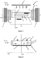
- la
figure 1 représente, de manière schématique, en vue de coupe, un mode de réalisation d'un dispositif de restauration d'éléments photovoltaïques ; - la
figure 2 représente, de manière schématique, en vue de coupe, un exemple d'un élément photovoltaïque en présence d'un champ magnétique ; - la
figure 3 représente, le tracé de la distribution en profondeur de la concentration des porteurs de charge minoritaires dans le substrat d'un élément photovoltaïque pour plusieurs valeurs de mobilités des électrons et des trous ; - la
figure 4 représente, le tracé de la variation de la concentration moyenne des porteurs de charge minoritaires au sein du substrat d'un élément photovoltaïque, en fonction de l'intensité du champ magnétique, selon un mode de réalisation ; - les
figures 5a et 5b représentent des tracés de la distribution en profondeur de la concentration des porteurs de charge minoritaires dans le substrat d'un élément photovoltaïque, éclairé respectivement par deux types de rayonnement et pour différentes valeurs de l'intensité du champ magnétique appliqué au substrat ; - la
figure 6 représente, le tracé du gain du temps de régénération de l'élément photovoltaïque en fonction de l'intensité du champ magnétique, selon un mode de réalisation. - Un procédé de traitement, ou de restauration, d'un élément photovoltaïque notamment une cellule solaire photovoltaïque, est décrit ci-après.
- Avantageusement, le procédé traite l'élément photovoltaïque contre la dégradation du rendement sous éclairement, par génération de porteurs de charge dans ledit élément. Le procédé tire profit de l'effet d'un champ magnétique transverse pour améliorer la cinétique et l'efficacité de restauration des éléments traités.
- Selon un mode de réalisation illustré aux
figures 1 et 2 , le procédé prévoit un élément photovoltaïque 10 comportant un substrat 1 à base de silicium. Le substrat 1 est muni d'une face avant 1a et d'une face arrière 1b opposées, et de préférence sensiblement parallèles, et il peut être à base de silicium amorphe, monocristallin ou multicristallin. Le substrat 1 est muni en surface, au niveau de la face 1a, d'au moins une région émettrice 1E. Une interface 24 sépare la région émettrice 1E d'une région de base 1B. Généralement, l'épaisseur de la région de base 1B est largement supérieure à l'épaisseur de la région émettrice 1E. Ainsi, par la suite on parlera de l'interface 24 entre la région émettrice 1E et le substrat 1. - La face avant 1a est destinée à recevoir une intensité lumineuse, pour générer préférentiellement un photocourant résultant. Le photocourant généré est généralement proportionnel à l'intensité lumineuse reçue en face avant 1a par le substrat 1.
- L'élément photovoltaïque 10 est préférentiellement une cellule solaire de type Al-BSF. L'élément photovoltaïque 10 peut être également une cellule photovoltaïque de type PERC ou PERT (PERC pour l'abréviation anglaise de « Passivated Emitter and Rear Cell » et PERT pour l'abréviation anglaise de « Passivated Emitter, Rear Totally diffused cell »). Une cellule solaire de type Al-BSF comporte une passivation par effet de champ à l'aide d'un fort dopage au niveau de la face arrière de la cellule. La barrière de potentiel induite par la différence de niveau de dopage entre la base et la face arrière tend à confiner les porteurs minoritaires dans la base et à les éloigner du bord de la cellule. Ce dopage est généralement réalisé grâce au contact en face arrière à base d'aluminium qui vient former un alliage avec le silicium lors du recuit. Dans ces conditions, une zone dopée P+ est formée sur l'ensemble de la face arrière de la cellule : on parle alors de champ de surface arrière ou BSF (BSF pour l'abréviation anglaise de « Back Surface Field »).
- Ainsi, la face arrière 1b du substrat 1 peut être recouverte par une couche en aluminium formant une prise de contact pour ledit élément photovoltaïque 10. La prise de contact en face avant est avantageusement formée par un contact ohmique à base d'aluminium. En fait, l'aluminium et l'argent possèdent une perméabilité magnétique proche de 1, permettant de manière avantageuse, d'atténuer la distorsion des lignes de champ magnétique au sein du substrat 1. Par ailleurs, le silicium qui constitue le matériau de base de l'élément photovoltaïque 10 a également une perméabilité magnétique proche de 1.
- Le procédé de restauration comporte une étape de génération de porteurs de charge dans le substrat 1 en le chauffant. Le chauffage du substrat est réalisé en maintenant le substrat 1 à une température comprise entre 20 °C et 230 °C.
- Préférentiellement, le procédé de restauration comporte une étape d'éclairement de l'élément photovoltaïque 10 configurée pour générer des porteurs de charge dans le substrat 1. Autrement dit, l'étape de génération des porteurs de charge est obtenue par éclairement du substrat 1.
- Selon le mode particulier illustré à la
figure 1 , la génération de porteurs de charge est réalisée par des moyens comportant préférentiellement une source lumineuse 2 éclairant l'élément photovoltaïque 10. Ce dernier, peut être éclairé par différents types de sources lumineuses. Par ailleurs, les moyens de génération de porteurs de charge peuvent également constituer une source de chaleur configurée à la fois pour éclairer le substrat 1 et pour le chauffer. - Avantageusement, l'élément photovoltaïque 10 reçoit un éclairement supérieur à 4000 W/m2 pendant le procédé de restauration.
- La génération de porteurs de charge peut être réalisée par éclairement et/ou par injection d'un courant électrique dans le substrat 1, notamment par une source de différence de potentiel externe par rapport au substrat 1.
- Comme illustré à la
figure 2 , le substrat 1 comporte préférentiellement au niveau de la face avant 1a des contacts électriques. En fait, le procédé comporte avantageusement une formation de contacts électriques 23 sur le substrat 1. L'étape de génération des porteurs de charge est obtenue par application d'une tension électrique externe aux contacts 23. - Ainsi, les moyens de génération de porteurs de charge dans le substrat 1, comportent en outre des moyens d'injection (non représentés aux figures) d'un courant électrique dans l'élément photovoltaïque 10. Préférentiellement, une densité de courant supérieure à 30 mA/cm2 est injectée dans l'élément 10 à traiter.
- Pour réaliser l'étape de chauffage, le substrat 1 est maintenu à une valeur de température comprise dans l'intervalle de température 20 °C - 230 °C, et de préférence entre 50 °C et 230 °C. La température peut être fixe ou varier dans la gamme décrite, durant la génération des porteurs de charge. Les étapes de chauffage de la cellule solaire 1 et d'injection des porteurs de charge dans le substrat 1 sont des étapes réalisées simultanément, afin de permettre à l'élément photovoltaïque 10 traité, de retrouver des performances stables sous des conditions normales de fonctionnement.
- De manière avantageuse, la température de l'élément photovoltaïque 10 est maintenue à une valeur ou une plage de température cible, comprise dans l'intervalle de température 120 °C - 210 °C. Le chauffage de l'élément photovoltaïque 10 peut être réalisé par une source externe de chaleur ou par les moyens de génération 2 de porteurs de charge, par exemple par des lampes halogènes.
- En outre, le procédé de traitement prévoit des moyens d'application 4 d'un champ magnétique B au substrat. Autrement dit, le procédé de traitement comporte une étape d'application d'un champ magnétique B traversant l'élément photovoltaïque 10. Comme illustré à la
figure 1 , le substrat 1 est soumis à un champ magnétique B ayant une composante Bc sensiblement parallèle à l'interface 24 entre la région émettrice 1E et le substrat 1. L'interface 24 représente l'interface entre les deux types opposés de dopage présents dans le substrat 1, autrement dit l'interface de la jonction p/n, formant la région de base 1B et la région émettrice 1E. - Généralement, l'interface 24 est parallèle à la face avant 1a et la face arrière 1b. Selon un mode de réalisation particulier, le substrat 1 est soumis à un champ magnétique B ayant une composante Bc sensiblement perpendiculaire à un axe (Ox) traversant la face avant 1a et la face arrière 1b.
- Par composante du champ magnétique B, on entend une composante selon un repère orthonormé (O, i, j, k). Préférentiellement, les faces 1a et 1b sont sensiblement parallèles, et l'axe (Ox) est sensiblement perpendiculaire aux faces 1a et 1b.
- L'élément photovoltaïque 10, autrement dit le substrat 1 comporte au niveau de la face 1b, un contact arrière 22 préférentiellement à base d'aluminium, générant un champ de surface arrière BSF. Le substrat 1 comporte également au niveau de la face avant 1a les contacts électriques 23. Ainsi, le mouvement des porteurs de charge 21 suit une direction moyenne 20 sensiblement perpendiculaire à l'interface 24, notamment aux faces 1a et 1b.
- Le champ magnétique B appliqué au substrat 1 est configuré, de sorte à ne pas être parallèle à la direction moyenne 20 du mouvement général des porteurs de charge 21. Sinon, la force de Lorentz F engendrée serait alors nulle, et le champ magnétique B n'aurait pas d'influence notable sur la concentration des porteurs de charge minoritaires 21 dans le substrat 1.
- Des simulations numériques par le logiciel PC1D développé par l'université « New South Wales » ont été réalisées pour étudier l'influence d'un champ magnétique sur la concentration des porteurs de charge minoritaires dans un élément photovoltaïque.
- Les simulations ont concerné des cellules solaires de type Al-BSF. La cellule Al-BSF étudiée comporte un substrat 1 en silicium de 200 µm d'épaisseur dopé p, et une concentration en charges libres majoritaires a l'équilibre de 6x10¹⁵ at/cm3. Les simulations numériques ont été réalisées en considérant la cellule solaire en circuit ouvert, et un éclairement en face avant par un rayonnement ayant un spectre de AM1.5G, autrement dit, ayant une irradiance de 1000 W/m2. En outre, les simulations numériques ont été réalisées en considérant que la durée de vie des porteurs minoritaires dans le substrat 1 de l'élément photovoltaïque 10 est égale à 10-3 s.
- La
figure 3 représente la distribution des porteurs de charges minoritaires en fonction de la profondeur du substrat 1, obtenue par les simulations numériques pour différentes valeurs de mobilité des électrons (µe) et des trous (µh) dans le substrat 1, lorsque l'on applique différentes valeurs de champ magnétique. Les résultats des simulations numériques tracés à lafigure 3 , indiquent clairement que la concentration des porteurs minoritaires augmente lorsque la mobilité des porteurs diminue. En outre, cette augmentation est obtenue sous des conditions d'éclairement favorables au phénomène de dégradation du rendement sous éclairement. - Les résultats des simulations montrent que l'application d'un champ magnétique transverse dans le substrat 1 entraîne une augmentation de la concentration des porteurs minoritaires.
- Selon le mode de réalisation avantageux des
figures 1 et 2 , le champ magnétique B est parallèle à l'interface 24 entre la région émettrice 1E et le substrat 1, ou la région de base 1B. Préférentiellement, le champ B est configuré de sorte à être perpendiculaire à l'axe (Ox). Autrement dit, la direction du champ magnétique B est dans le plan (O, j, k). De ce fait, une force parallèle à l'interface 24 (i.e. aux faces 1a et 1b du substrat 1) est appliquée aux porteurs de charge 21 en mouvement. L'amplitude de cette force générée est alors maximisée, entrainant une forte diminution de la mobilité des porteurs de charge. Pour une intensité fixée du champ magnétique B, une telle orientation du champ magnétique génère avantageusement une augmentation optimale de la quantité des porteurs de charge minoritaires au sein du substrat 1, permettant ainsi une amélioration de la cinétique du procédé de restauration. - La
figure 4 illustre l'évolution de la concentration moyenne des porteurs de charge minoritaires Δn en fonction de l'intensité du champ magnétique appliqué au substrat 1. La cellule étudiée est la même que celle décrite ci-dessus et dont les résultats des simulations sont tracés à lafigure 3 . En outre, les calculs ont été effectués en considérant que le procédé de restauration a été réalisé à une température de 127 °C, et que le champ magnétique B était perpendiculaire à l'axe (Ox). Les simulations numériques ont été réalisées en considérant un éclairement en face avant par un rayonnement ayant un spectre de AM1.5G, autrement dit, ayant une irradiance de 1000 W/m2. - Selon un mode de réalisation préférentiel, l'éclairement est obtenu en utilisant une lumière ayant une longueur d'onde supérieure ou égale à 500 nm, et de préférence supérieure ou égale à 800 nm, et inférieure ou égale à 1300 nm, et de préférence inférieure ou égale à 1000 nm.
- La
figure 4 montre que la concentration moyenne Δn augmente avec l'augmentation de l'intensité du champ magnétique B appliqué au substrat 1 dans le procédé de traitement. Cette augmentation est d'autant plus marquante que l'intensité du champ magnétique B est supérieure à 0,001 T. Avantageusement, le procédé de traitement est réalisé en utilisant un champ magnétique B dont la composante Bc a une intensité comprise entre 10-4 T et 5x10⁻¹ T et avantageusement supérieure ou égale à 0,001 T. - Selon un mode de réalisation avantageux, l'étape d'éclairement de l'élément photovoltaïque 10 est réalisée par un rayonnement monochromatique infrarouge (R). Préférentiellement, le rayonnement (R) a une longueur d'onde d'environ 1000 nm. Les
figures 5a et 5b illustrent la distribution en profondeur (l'origine étant la face avant 1a) de la concentration moyenne des porteurs de charge minoritaires Δn. Chacune desfigures 5a et 5b représente trois distributions correspondant à trois intensités du champ magnétique B perpendiculaire à l'axe (Ox) égales à 10-4, 10-3 et 10-2 T. - Les calculs ont été effectués pour des procédés de restauration de l'élément photovoltaïque 10 réalisés à une température de 25 °C et à une intensité d'éclairement de 1000 W/m2. La
figure 5a correspond aux résultats obtenus pour un procédé utilisant un éclairement en face avant par un spectre de type AM1.5G, alors que les résultats de lafigure 5b correspondent à un éclairement en face avant par un rayonnement monochromatique infrarouge dont la longueur d'onde est égale à 1000 nm. - Les
figures 5a et 5b montrent l'effet positif résultant de l'utilisation d'un fort champ magnétique en combinaison avec un éclairement par un rayonnement infrarouge. En effet, cette combinaison permet d'obtenir avantageusement une distribution uniforme de la concentration moyenne des porteurs de charge Δn. En plus de l'uniformité de la distribution de la concentration moyenne, l'utilisation d'un éclairement monochromatique infrarouge permet une nette augmentation de la concentration Δn, notamment au niveau de la région émettrice 1E et de l'interface 24 du substrat 1 à traiter, autrement dit au niveau de la jonction p/n. Cette augmentation et cette uniformité permettent de manière avantageuse une guérison plus rapide et plus uniforme, selon la profondeur, de l'élément photovoltaïque 10 à traiter. - L'application d'un champ magnétique transverse dans le substrat 1 à traiter entraîne une augmentation de la concentration moyenne Δn. Avantageusement, le procédé permet une amélioration très significative de la cinétique de restauration des éléments photovoltaïques des effets de dégradation du rendement sous éclairement.
- L'accélération de la cinétique de restauration se traduit par une nette diminution du temps de régénération de l'élément photovoltaïque 10. Par temps de régénération, on entend le temps de traitement de l'élément photovoltaïque 10 nécessaire pour qu'il retrouve des performances stables sous des conditions normales de fonctionnement.
- La
figure 6 illustre l'évolution, en fonction de l'intensité du champ magnétique, du rapport de temps de régénération de l'élément photovoltaïque 10 en utilisant un champ magnétique tLIR-B, sur le temps de régénération de l'élément photovoltaïque avec un procédé standard tLIR. Par procédé standard, on entend un procédé n'utilisant pas un champ magnétique appliqué à l'élément photovoltaïque. A l'exception de l'application d'un champ magnétique, les deux procédés ont les mêmes conditions de mise en oeuvre. Les calculs ont été effectués en considérant que les procédés de restauration de l'élément photovoltaïque 10 ont été réalisés à une température de 127 °C, et en utilisant un rayonnement monochromatique infrarouge avec une irradiance de 1000 W/m2. - La
figure 6 montre clairement que l'utilisation d'un champ magnétique appliqué à l'élément photovoltaïque 10 pendant le procédé de restauration permet de réduire considérablement le temps de régénération, notamment pour des intensités du champ magnétique supérieures à 5x10⁻³ T. Par exemple, en utilisant un champ magnétique dont l'intensité est égale à 0,01 T, le temps de régénération (tLIR-B) correspond au temps de régénération par le procédé standard (tLIR) divisé à peu près par 5 pour l'élément photovoltaïque 10 à base d'un substrat 1 présentant une durée de vie dans le volume de 10-3 s. - Le procédé de restauration utilisant un champ magnétique transverse appliqué à l'élément photovoltaïque 10, permet de réduire considérablement le temps de régénération. Ainsi, le procédé de restauration est avantageusement compatible avec les procédés industriels de fabrication des cellules solaires photovoltaïques.
- Par ailleurs, en fixant le temps de régénération, le procédé de restauration utilisant un champ magnétique permet, de manière avantageuse, de réduire l'intensité d'éclairement, ou l'irradiance. A titre d'exemple, l'utilisation d'un champ magnétique appliqué à l'élément photovoltaïque 10 ayant une intensité de 0,01 T, permet de diviser à peu près par 3 l'intensité d'éclairement nécessaire pour la régénération pour le substrat présentant une durée de vie dans le volume de 10-3 s. Ainsi, il est envisageable d'utiliser des sources d'éclairement moins intenses consommant moins d'énergie.
- Les différentes expériences et les différents calculs réalisés lors de l'étude du procédé de traitement utilisant un champ magnétique transverse ont permis d'établir des formules mathématiques reliant le temps nécessaire à la régénération complète tLIR-B en fonction des principaux paramètres du procédé. En effet, les formules mathématiques donnent le temps tLIR-B en fonction de la température T en Kelvin de l'élément photovoltaïque à traiter, de l'intensité du champ magnétique transverse Bc en tesla appliqué à l'élément photovoltaïque 10 à traiter, et de l'irradiance I en sun. L'irradiance correspond à l'intensité du rayonnement projeté sur la face avant 1a du substrat 1. Dans le système international d'unités, 1 sun correspond à 1000 W/m2. Les formules mathématiques ont été établies pour des éléments photovoltaïques 10 à base de substrats en silicium dopés p, et pour des intensités de champ magnétique transverse Bc comprises entre 10-4 à 0,4 T.
- Ainsi, selon un mode préférentiel de réalisation, l'élément photovoltaïque 10 est réalisé à partir d'un substrat en silicium dopé bore avec une concentration comprise entre 4x10¹⁴ at/cm3 et 7x10¹⁶ at/cm3. Selon ce mode de réalisation, le temps de traitement t en secondes est avantageusement supérieure ou égale à :

- Selon un autre mode préférentiel de réalisation, l'élément photovoltaïque 10 est réalisé à partir d'un substrat 1 en silicium dopé bore avec une concentration strictement supérieure à 7x10¹⁶ at/cm3. Selon ce mode de réalisation, le temps de traitement t en secondes est supérieure ou égale à :

- Par ailleurs, on prévoit également un dispositif destiné à réaliser le procédé de traitement décrit selon les différents modes de réalisation présentés ci-dessus.
- Selon un mode de réalisation illustré à la
figure 1 , le dispositif de restauration 20 est configuré pour guérir l'élément photovoltaïque 10. Ce dernier comporte le substrat 1 muni de la face avant 1a et de la face arrière 1b opposées et de préférence sensiblement parallèles. La face avant 1a est destinée à recevoir une intensité lumineuse, ou une irradiance. Le substrat 1 comporte la région émettrice 1E au niveau de la face 1a, et la région de base 1B. Le dispositif 20 comporte des moyens de génération 2 de porteurs de charge dans le substrat 1. - Les moyens de génération 2 de porteurs de charge comportent préférentiellement la source lumineuse 2 éclairant l'élément photovoltaïque 10 à traiter. La source lumineuse 2 peut comporter des lampes monochromatiques ou multispéctrales permettant de produire un faisceau lumineux incident ayant une longueur d'onde préférentiellement comprise entre 300 et 1300 nm.
- La source lumineuse 2 peut aussi bien comporter des lampes halogènes ou xénon. Selon un exemple de réalisation la source lumineuse est formée par des lampes en xénon permettant d'avoir un éclairement continu de l'élément photovoltaïque 10 à traiter avec une irradiance d'environ 1000 W/m2. Avantageusement, la source lumineuse 2 est configurée pour fournir un éclairement intense de manière à ce que les éléments photovoltaïques 10 reçoivent un éclairement supérieur à 5x10⁴ W/m2.
- Par ailleurs, la source lumineuse 2 peut comporter des LED ou encore une source laser, qui génère avantageusement un éclairement intense. L'utilisation d'une source laser ou des LED permet avantageusement une réduction de la consommation énergétique, en comparaison avec les autres sources lumineuses.
- Le dispositif de traitement 20 comporte également des moyens de traitement thermique 3 configurés pour maintenir le substrat 1 à une température comprise dans l'intervalle de température 20 °C - 230 °C, et de préférence dans l'intervalle de température 50 °C - 230 °C. Les moyens de traitement thermique 3 peuvent comporter une source de chaleur. Par ailleurs, les moyens de génération 2 de porteurs de charge peuvent également former les moyens de traitement thermique 3. Par exemple des lampes halogènes peuvent éclairer la cellule solaire 1 tout en la réchauffant.
- Comme illustré à la
figure 1 , le contrôle de la température du substrat 1 est préférentiellement réalisé par une enceinte 3 configurée pour maintenir la température du substrat 1 à une valeur ou une plage de température cible. L'enceinte 3 peut être un four classique muni de capteurs de température configurés pour mesurer la température du substrat 1. Le four peut également comporter un dispositif de régulation de la température de l'élément photovoltaïque 10. Le dispositif de régulation est connecté à un circuit de commande configuré pour contrôler la température du four et le dispositif de régulation en fonction de la température de l'élément photovoltaïque 10. - Par ailleurs, les moyens de contrôle 3 de la température du substrat 1 sont configurés pour que l'élément photovoltaïque 10 soit éclairé. Par exemple, l'enceinte 3 de maintien de la température de l'élément photovoltaïque 10 peut comporter la source lumineuse 2.
- Préférentiellement, l'enceinte 3 comporte une paroi transparente au rayonnement émis par la source d'éclairement 2. La paroi transparente est interposée entre la source d'éclairement 3 et la face avant 1a de l'élément photovoltaïque 10, de sorte à laisser passer le rayonnement émis par la source 2, éclairant ainsi la face avant 1a du substrat 1.
- En outre, le dispositif comporte des moyens d'application 4 d'un champ magnétique B configurés pour que le champ magnétique B ait une composante Bc sensiblement parallèle à l'interface 24 entre la région émettrice 1E et le substrat 1. Préférentiellement, la composante Bc est perpendiculaire à un axe (Ox) traversant la face avant 1a et la face arrière 1b.
- Selon un exemple de réalisation, les moyens d'application 4 comportent deux aimants permanents 11 et 12 séparés par un entrefer 13. Les aimants 11 et 12 sont montés sur un support 14 de sorte qu'ils soient disposés en regard. L'aimant 11 comporte une face 11' disposée en regard d'une face 12' de l'aimant 12. Les aimants 11 et 12 sont configurés de sorte que les faces 11' et 12' disposées en regard aient des pôles magnétiques opposés (N et S).
- Les aimants 11 et 12 sont configurés pour créer le champ magnétique transverse B balayant l'espace de l'entrefer 13. En fonction de l'architecture et de la composition de l'élément photovoltaïque 10 ou le substrat 1, et de l'enceinte 3, les aimants 11 et 12 sont disposés de sorte à créer le champ magnétique B ayant une composante Bc sensiblement parallèle à l'interface 24. Préférentiellement, l'interface 24 est parallèle aux faces 1a et 1b, et les aimants 11 et 12 sont configurés et disposés de sorte que le champ magnétique B créé ait une direction parallèle aux faces 1a et 1b.
- Par ailleurs, l'entrefer 13 est configuré pour comporter l'élément photovoltaïque 10 à traiter. Autrement dit, l'entrefer 13 est configuré pour abriter l'enceinte 3 comportant l'élément photovoltaïque 10. De manière préférentielle, le dispositif 20 comporte des moyens de fixation (non représentés à la figure) des éléments situés dans l'entrefer 13, notamment des moyens de fixation de l'élément photovoltaïque 10. La fixation des éléments disposés dans l'entrefer 13 permet d'éviter la distorsion des lignes de champ magnétique créées dans le substrat 1. Ce qui permet d'avoir un procédé de traitement stable et homogène dans le substrat 1.
- Préférentiellement, l'enceinte 3 est à base de matériaux ayant des perméabilités magnétiques relatives proches de 1. Par exemple, l'enceinte 3 peut être à base d'aluminium. En effet, un matériau ayant une perméabilité magnétique proche de 1, permet de manière avantageuse, d'atténuer la distorsion des lignes de champ magnétique au sein du substrat 1. Ainsi, les aimants 11 et 12 créent un flux homogène du champ magnétique B dans le substrat 1 disposé dans l'entrefer 13.
- Selon un exemple de réalisation, les deux aimants 11 et 12 sont de type Nb ayant une densité de flux résiduel de 1320 mT, et un champ magnétique coercitif supérieur à 11 Oesterd. Les aimants 11 et 12 sont des barreaux cylindriques ayant une section circulaire d'un un rayon de 100 mm. Les barreaux cylindriques 11 et 12 ont une épaisseur de 30 mm. Par épaisseur, on entend la dimension des aimants 11 et 12 selon l'axe (Oy). Les aimants 11 et 12 sont séparés d'une distance d'environ 150 mm. Autrement dit, la dimension de l'entrefer 13 selon l'axe (Oy) est d'environ 150 mm. Ainsi, l'entrefer 13 peut abriter un élément photovoltaïque commercial disposée de sorte que les faces 1a et 1b soient parallèles à l'axe (Oy).
- En utilisant des formules mathématiques connues de l'état de la technique, la densité de flux, autrement dit l'intensité du champ magnétique B le long de l'axe (Oy) de l'entrefer 13 peut être calculée à partir des caractéristiques et des dimensions des aimants 11 et 12.
- Ainsi, selon l'exemple de réalisation décrit ci-dessus, les aimants 11 e 12 permettent de créer dans l'entrefer 13, un champ magnétique transverse B ayant une direction parallèle à l'axe (Oy) et une intensité comprise entre 250 mT et 400 mT.
- Selon un mode de réalisation non illustré aux figures, les moyens d'application 4 du champ magnétique B comportent un électroaimant. En effet, le champ magnétique B peut être généré par les aimants permanents 11 et 12 et/ou par un électroaimant comportant par exemple une bobine électromagnétique. La distribution finale des lignes de champ magnétique dépend de la configuration finale de l'installation des aimants 11 et 12 et/ou de l'électroaimant. Cette distribution peut être non uniforme engendrant ainsi une irrégularité de l'intensité du champ magnétique B dans le substrat 1 à traiter.
- Dans tous les cas, l'installation doit être dimensionnée, et les moyens d'application 4 doivent être arrangés de manière à garantir une valeur minimale de l'intensité du champ magnétique appliqué à un élément photovoltaïque 10 à traiter, et une composante Bc sensiblement parallèle à l'interface 24, et préférentiellement perpendiculaire à l'axe (Ox) traversant la face avant 1a et la face arrière 1b.
- Selon un autre mode de réalisation, les moyens de génération 2 de porteurs de charge dans le substrat 1 comportent des moyens d'injection d'un courant électrique dans le substrat 1. Les moyens d'injection du courant sont externes à l'élément photovoltaïque 10.
- Les moyens d'injection d'un courant électrique dans le substrat 1 peuvent former un complément à une source de lumière éclairant l'élément photovoltaïque 10. Par ailleurs, les moyens d'injection d'un courant peuvent également remplacer la source de lumière configurée pour générer des porteurs de charges minoritaires au sein de l'élément photovoltaïque 10 à traiter.
- Les moyens d'injection peuvent comporter des pointes, reliées à un générateur de différence de potentiel. Lesdites pointes sont configurées pour être en contact avec les contacts 23 de l'élément photovoltaïque 10 pour y injecter un courant électrique.
- Le générateur de différence de potentiel est configuré pour imposer aux bornes de l'élément photovoltaïque 10 une différence de potentiel supérieure à la tension de l'élément photovoltaïque en circuit ouvert. Préférentiellement, le générateur de différence de potentiel est configuré pour imposer à l'élément photovoltaïque 10, une différence de potentielle typiquement supérieur à 0,6 ou 0,75 V. Par ailleurs, le courant à injecter dans l'élément photovoltaïque 10 dépend des caractéristiques de ce dernier et de la concentration de porteurs qu'on cherche à injecter.
- Selon un autre mode de réalisation, le dispositif de traitement 20 est configuré pour traiter plusieurs éléments photovoltaïques simultanément. L'enceinte 3 est ainsi configurée pour accueillir plusieurs éléments photovoltaïques disposés dans l'entrefer 13.
- Avantageusement, les éléments photovoltaïques sont disposés parallèlement à l'axe (Oy) de manière à être l'un au dessus de l'autre de sorte que l'axe (Ox) traverse tous les éléments photovoltaïques empilés. Selon ce mode de réalisation, les moyens d'injection 2 de porteurs de charge sont avantageusement constitués par des moyens d'injection d'un courant électrique. De manière préférentielle, les éléments photovoltaïques à traiter sont électriquement connectés en série.
Claims (11)
- Procédé de traitement d'un élément photovoltaïque (10) contre la dégradation du rendement sous éclairement, comportant au moins les étapes suivantes :- prévoir ledit élément (10) comportant un substrat (1) à base de silicium, muni en surface d'au moins une région émettrice (1E);- générer des porteurs de charge dans le substrat (1), tout en maintenant le substrat (1) à une température comprise dans un intervalle de température compris entre 20°C et 230 °C et de préférence entre 50°C et 230°C;caractérisé en ce que le substrat (1) est soumis à un champ magnétique (B) pendant l'étape de génération des porteurs de charge, le champ magnétique (B) ayant une composante (Bc) sensiblement parallèle à l'interface (24) entre la région émettrice (1E) et le substrat (1),
et en ce que la composante (Bc) du champ magnétique (B) a une intensité comprise entre 10-4 T et 5.10-1 T et avantageusement supérieure à 10-3 T. - Procédé selon la revendication 1, caractérisé en ce que l'étape de génération des porteurs de charge est obtenue par éclairement du substrat (1).
- Procédé selon la revendication 2, caractérisé en ce que l'éclairement est obtenu en utilisant une lumière ayant une longueur d'onde supérieure ou égale à 500nm, et de préférence supérieure ou égale 800nm, et inférieure ou égale à 1300nm, et de préférence inférieure ou égale à 1000nm.
- Procédé de traitement selon la revendication 1, caractérisé en ce que :- le substrat (1) est en silicium dopé bore avec une concentration comprise entre 4,0x10¹⁴ at/cm-3 et 7,0x10¹⁶ at/cm-3, et- le temps de traitement (t) de l'élément photovoltaïque (10), en secondes, est supérieure ou égale à :
 - T correspond à la température en kelvin du substrat (1) ;- Bc correspond à l'intensité en Tesla de ladite composante (Bc) du champ magnétique (B) ;- I correspond à l'irradiance en sun du rayonnement projeté sur la surface (1a) du substrat (1) ;- C1 correspond à une première constante comprise entre 1,3x10⁻⁵ et 3,2x10⁻⁵ et préférentiellement égale à 1,7x10⁻⁵ ;- C2 correspond à une deuxième constante comprise entre 1,00 et 32,0 et préférentiellement égale à 4,32 ;- C3 correspond à une troisième constante comprise entre -1,00 et-2,00 et préférentiellement égale à -1,62 ;- C4 correspond à une quatrième constante comprise entre 6562 et 8523 et préférentiellement égale à 7500.
 - Procédé de traitement selon la revendication 1, caractérisé en ce que :- le substrat (1) est en silicium dopé bore avec une concentration strictement supérieure à 7x10¹⁶ at/cm-3 ; et- le temps de traitement (t) de l'élément photovoltaïque (10), en secondes, est supérieure ou égale à :
 - T correspond à la température en kelvin du substrat (1) ;- Bc correspond à l'intensité en tesla de ladite composante (Bc) du champ magnétique (B) ;- I correspond à l'irradiance en sun du rayonnement projeté sur la surface (1a) du substrat (1) ;- C'1 correspond à une première constante additionnelle comprise entre 1,2x10⁻⁸ et 1,9x10⁻⁸ et préférentiellement égale à 1,51x10⁻⁸ ;- C'2 correspond à une deuxième constante additionnelle comprise entre 1,00 to 32,0 et préférentiellement égale à 4,32 ;- C'3 correspond à une troisième constante additionnelle comprise entre 2,5x10⁻⁸ et 4,0x10⁻⁸ et préférentiellement égale à 4,0x10⁻⁸ ; et- C'4 correspond à une quatrième constante additionnelle comprise entre 6562 et 8523 et préférentiellement égale à 7500.
 - Procédé selon l'une quelconque des revendications 1 à 5, caractérisé en ce qu'il comporte une étape de formation de contacts électriques (23) sur le substrat (1) et en ce que l'étape de génération des porteurs de charge comporte une application d'une tension électrique externe aux contacts électriques (23).
- Dispositif de traitement d'un élément photovoltaïque (10) contre la dégradation du rendement sous éclairement, l'élément photovoltaïque (10) comprenant un substrat (1) en silicium muni d'au moins une région émettrice (1E) comportant :- des moyens de génération (2) de porteurs de charge dans le substrat (1),- des moyens de traitement thermique (3) configurés pour maintenir le substrat (1) à une température comprise dans l'intervalle de température entre 20 °C et 230 °C et de préférence entre 50°C et 230°C ; et- des moyens d'application (4) d'un champ magnétique (B) balayant un entrefer (13) configuré pour comporter l'élément photovoltaïque (10), lesdits moyens d'application (4) étant configurés pour que le champ magnétique (B) ait une composante (Bc) sensiblement parallèle à l'interface (24) entre la région émettrice (1E) et le substrat (1), et pour que la composante (Bc) du champ magnétique (B) a une intensité comprise entre 10-4 T et 5.10-1 T et avantageusement supérieure à 10-3 T.
- Dispositif selon la revendication 7, caractérisé en ce que les moyens d'application (4) d'un champ magnétique (B) comportent des aimants permanents (11', 12').
- Dispositif selon l'une des revendications 7 et 8, caractérisé en ce que les moyens d'application (4) d'un champ magnétique (B) comportent un électroaimant.
- Dispositif selon la revendication 7, caractérisé en ce que les moyens de génération (2) de porteurs de charge dans l'élément photovoltaïque (10) comportent une source lumineuse destinée à éclairer l'élément photovoltaïque (10).
- Dispositif selon la revendication 7, caractérisé en ce que le substrat (1) est muni de contacts électriques (23) et en ce que les moyens de génération (2) de porteurs de charge dans le substrat (1) comportent des moyens d'application d'une tension électrique externe aux contacts électriques (23).
Applications Claiming Priority (1)
| Application Number | Priority Date | Filing Date | Title |
|---|---|---|---|
| FR1461000A FR3028669B1 (fr) | 2014-11-14 | 2014-11-14 | Procede de restauration de cellules solaires photovoltaiques a base de silicium |
Publications (2)
| Publication Number | Publication Date |
|---|---|
| EP3021365A1 EP3021365A1 (fr) | 2016-05-18 |
| EP3021365B1 true EP3021365B1 (fr) | 2019-01-09 |
Family
ID=52130498
Family Applications (1)
| Application Number | Title | Priority Date | Filing Date |
|---|---|---|---|
| EP15194533.4A Active EP3021365B1 (fr) | 2014-11-14 | 2015-11-13 | Procédé de restauration de cellules solaires photovoltaïques à base de silicium |
Country Status (4)
| Country | Link |
|---|---|
| US (1) | US20160141443A1 (fr) |
| EP (1) | EP3021365B1 (fr) |
| CN (1) | CN105702804A (fr) |
| FR (1) | FR3028669B1 (fr) |
Families Citing this family (4)
| Publication number | Priority date | Publication date | Assignee | Title |
|---|---|---|---|---|
| CN107887471B (zh) * | 2017-09-29 | 2019-05-21 | 苏州润阳光伏科技有限公司 | 降低p型太阳电池光致衰减的方法 |
| CN112213261A (zh) * | 2020-09-14 | 2021-01-12 | 长江存储科技有限责任公司 | 氙灯光源及光学量测机台 |
| KR102568449B1 (ko) * | 2021-06-15 | 2023-08-23 | 재단법인 구미전자정보기술원 | 태양전지 모듈의 광열화 현상 및 회복 특성 분석 장치와 그 방법 |
| CN116247131B (zh) * | 2023-02-03 | 2024-05-10 | 通威太阳能(安徽)有限公司 | 降低太阳电池转换效率衰减的方法 |
Family Cites Families (5)
| Publication number | Priority date | Publication date | Assignee | Title |
|---|---|---|---|---|
| JPS59159167A (ja) * | 1983-03-01 | 1984-09-08 | Zenko Hirose | アモルフアスシリコン膜の形成方法 |
| EP1732142A1 (fr) * | 2005-06-09 | 2006-12-13 | Shell Solar GmbH | Si cellule solaire et son procédé de fabrication |
| DE102006012920B3 (de) | 2006-03-21 | 2008-01-24 | Universität Konstanz | Verfahren zum Herstellen eines Photovoltaikelements mit stabilisiertem Wirkungsgrad |
| US20140124030A1 (en) * | 2011-06-30 | 2014-05-08 | Kaneka Corporation | Thin film solar cell and method for manufacturing same |
| US20140008234A1 (en) * | 2012-07-09 | 2014-01-09 | Rohm And Haas Electronic Materials Llc | Method of metal plating semiconductors |
-
2014
- 2014-11-14 FR FR1461000A patent/FR3028669B1/fr not_active Expired - Fee Related
-
2015
- 2015-11-13 EP EP15194533.4A patent/EP3021365B1/fr active Active
- 2015-11-16 US US14/942,423 patent/US20160141443A1/en not_active Abandoned
- 2015-11-16 CN CN201511035932.0A patent/CN105702804A/zh active Pending
Non-Patent Citations (1)
| Title |
|---|
| None * |
Also Published As
| Publication number | Publication date |
|---|---|
| FR3028669B1 (fr) | 2018-03-16 |
| CN105702804A (zh) | 2016-06-22 |
| US20160141443A1 (en) | 2016-05-19 |
| EP3021365A1 (fr) | 2016-05-18 |
| FR3028669A1 (fr) | 2016-05-20 |
Similar Documents
| Publication | Publication Date | Title |
|---|---|---|
| EP3021365B1 (fr) | Procédé de restauration de cellules solaires photovoltaïques à base de silicium | |
| EP0770268A1 (fr) | Procede de fabrication d'un materiau ou dispositif photovoltaique, materiau ou dispositif ainsi obtenu et photopile comprenant un tel materiau ou dispositif | |
| FR2475068A1 (fr) | Procede de dopage de semi-conducteurs | |
| EP4004986A1 (fr) | Procédé de traitement d'un empilement obtenu lors de la fabrication d'une cellule photovoltaïque a hétérojonction | |
| EP3012876A1 (fr) | Procede de fabrication d'une photodiode a faible bruit | |
| EP2786426B1 (fr) | Structure semiconductrice apte a recevoir un rayonnement électromagnétique, composant semiconducteur et procédé de fabrication d'une telle structure semiconductrice | |
| CA2745500A1 (fr) | Module photovoltaique comprenant une electrode transparente conductrice d'epaisseur variable et procedes de fabrication d'un tel module | |
| EP2937902B1 (fr) | Matrice de photodiodes en cdhgte | |
| CA2577186A1 (fr) | Detection a base de diamant synthetique | |
| EP2907154A1 (fr) | Photocathode semi-transparente à taux d'absorption amélioré | |
| Zerhouni et al. | Optimisation d’un système à énergie verte avec validation pratique | |
| EP0012181A2 (fr) | Convertisseur d'énergie solaire au silicium | |
| EP3660928B1 (fr) | Procédé de fabrication de cellules photovoltaiques | |
| Bruns et al. | Improved efficiency of crystalline silicon solar cells due to he+ implantation | |
| WO2014136082A1 (fr) | Plaquette de silicium monolithique presentant une alternance de zones dopees n et de zones dopees p | |
| Abramyan et al. | Effect of liquid dielectrics on the efficiency of silicon solar cells | |
| FR3047350A1 (fr) | ||
| EP3242335B1 (fr) | Procédé de fabrication d'une cellule photovoltaïque à hétérojonction | |
| EP3498893B1 (fr) | Procede d'extraction d'impuretes metalliques d'une plaquette de silicium cristallin | |
| Lin et al. | Enhanced efficiency of silicon-based solar cell by surface plasmon resonance effects over device electrode | |
| EP4305674A1 (fr) | Procédé et système de traitement d'un empilement destiné à la fabrication d'une cellule photovoltaïque à hétérojonction | |
| FR3074815A1 (fr) | Procede d'extraction d'impuretes metalliques d'une plaquette de silicium cristallin | |
| Joshi et al. | Impact of Light-and Elevated Temperature-Induced Degradation on PERC Solar Cells | |
| FR3047351A1 (fr) | ||
| Way | Fabrication of a-Si and a-InGaN Photovoltaics by Plasma Sputtering |
Legal Events
| Date | Code | Title | Description |
|---|---|---|---|
| PUAI | Public reference made under article 153(3) epc to a published international application that has entered the european phase |
Free format text: ORIGINAL CODE: 0009012 |
|
| AK | Designated contracting states |
Kind code of ref document: A1 Designated state(s): AL AT BE BG CH CY CZ DE DK EE ES FI FR GB GR HR HU IE IS IT LI LT LU LV MC MK MT NL NO PL PT RO RS SE SI SK SM TR |
|
| AX | Request for extension of the european patent |
Extension state: BA ME |
|
| STAA | Information on the status of an ep patent application or granted ep patent |
Free format text: STATUS: REQUEST FOR EXAMINATION WAS MADE |
|
| 17P | Request for examination filed |
Effective date: 20161117 |
|
| RBV | Designated contracting states (corrected) |
Designated state(s): AL AT BE BG CH CY CZ DE DK EE ES FI FR GB GR HR HU IE IS IT LI LT LU LV MC MK MT NL NO PL PT RO RS SE SI SK SM TR |
|
| GRAP | Despatch of communication of intention to grant a patent |
Free format text: ORIGINAL CODE: EPIDOSNIGR1 |
|
| STAA | Information on the status of an ep patent application or granted ep patent |
Free format text: STATUS: GRANT OF PATENT IS INTENDED |
|
| INTG | Intention to grant announced |
Effective date: 20180803 |
|
| GRAS | Grant fee paid |
Free format text: ORIGINAL CODE: EPIDOSNIGR3 |
|
| GRAA | (expected) grant |
Free format text: ORIGINAL CODE: 0009210 |
|
| STAA | Information on the status of an ep patent application or granted ep patent |
Free format text: STATUS: THE PATENT HAS BEEN GRANTED |
|
| AK | Designated contracting states |
Kind code of ref document: B1 Designated state(s): AL AT BE BG CH CY CZ DE DK EE ES FI FR GB GR HR HU IE IS IT LI LT LU LV MC MK MT NL NO PL PT RO RS SE SI SK SM TR |
|
| REG | Reference to a national code |
Ref country code: GB Ref legal event code: FG4D Free format text: NOT ENGLISH |
|
| REG | Reference to a national code |
Ref country code: CH Ref legal event code: EP Ref country code: AT Ref legal event code: REF Ref document number: 1088400 Country of ref document: AT Kind code of ref document: T Effective date: 20190115 |
|
| REG | Reference to a national code |
Ref country code: DE Ref legal event code: R096 Ref document number: 602015023116 Country of ref document: DE |
|
| REG | Reference to a national code |
Ref country code: IE Ref legal event code: FG4D Free format text: LANGUAGE OF EP DOCUMENT: FRENCH |
|
| REG | Reference to a national code |
Ref country code: NO Ref legal event code: T2 Effective date: 20190109 |
|
| REG | Reference to a national code |
Ref country code: NL Ref legal event code: MP Effective date: 20190109 |
|
| REG | Reference to a national code |
Ref country code: LT Ref legal event code: MG4D |
|
| PG25 | Lapsed in a contracting state [announced via postgrant information from national office to epo] |
Ref country code: NL Free format text: LAPSE BECAUSE OF FAILURE TO SUBMIT A TRANSLATION OF THE DESCRIPTION OR TO PAY THE FEE WITHIN THE PRESCRIBED TIME-LIMIT Effective date: 20190109 |
|
| REG | Reference to a national code |
Ref country code: AT Ref legal event code: MK05 Ref document number: 1088400 Country of ref document: AT Kind code of ref document: T Effective date: 20190109 |
|
| PG25 | Lapsed in a contracting state [announced via postgrant information from national office to epo] |
Ref country code: FI Free format text: LAPSE BECAUSE OF FAILURE TO SUBMIT A TRANSLATION OF THE DESCRIPTION OR TO PAY THE FEE WITHIN THE PRESCRIBED TIME-LIMIT Effective date: 20190109 Ref country code: PT Free format text: LAPSE BECAUSE OF FAILURE TO SUBMIT A TRANSLATION OF THE DESCRIPTION OR TO PAY THE FEE WITHIN THE PRESCRIBED TIME-LIMIT Effective date: 20190509 Ref country code: PL Free format text: LAPSE BECAUSE OF FAILURE TO SUBMIT A TRANSLATION OF THE DESCRIPTION OR TO PAY THE FEE WITHIN THE PRESCRIBED TIME-LIMIT Effective date: 20190109 Ref country code: SE Free format text: LAPSE BECAUSE OF FAILURE TO SUBMIT A TRANSLATION OF THE DESCRIPTION OR TO PAY THE FEE WITHIN THE PRESCRIBED TIME-LIMIT Effective date: 20190109 Ref country code: ES Free format text: LAPSE BECAUSE OF FAILURE TO SUBMIT A TRANSLATION OF THE DESCRIPTION OR TO PAY THE FEE WITHIN THE PRESCRIBED TIME-LIMIT Effective date: 20190109 Ref country code: LT Free format text: LAPSE BECAUSE OF FAILURE TO SUBMIT A TRANSLATION OF THE DESCRIPTION OR TO PAY THE FEE WITHIN THE PRESCRIBED TIME-LIMIT Effective date: 20190109 |
|
| PG25 | Lapsed in a contracting state [announced via postgrant information from national office to epo] |
Ref country code: RS Free format text: LAPSE BECAUSE OF FAILURE TO SUBMIT A TRANSLATION OF THE DESCRIPTION OR TO PAY THE FEE WITHIN THE PRESCRIBED TIME-LIMIT Effective date: 20190109 Ref country code: LV Free format text: LAPSE BECAUSE OF FAILURE TO SUBMIT A TRANSLATION OF THE DESCRIPTION OR TO PAY THE FEE WITHIN THE PRESCRIBED TIME-LIMIT Effective date: 20190109 Ref country code: BG Free format text: LAPSE BECAUSE OF FAILURE TO SUBMIT A TRANSLATION OF THE DESCRIPTION OR TO PAY THE FEE WITHIN THE PRESCRIBED TIME-LIMIT Effective date: 20190409 Ref country code: GR Free format text: LAPSE BECAUSE OF FAILURE TO SUBMIT A TRANSLATION OF THE DESCRIPTION OR TO PAY THE FEE WITHIN THE PRESCRIBED TIME-LIMIT Effective date: 20190410 Ref country code: IS Free format text: LAPSE BECAUSE OF FAILURE TO SUBMIT A TRANSLATION OF THE DESCRIPTION OR TO PAY THE FEE WITHIN THE PRESCRIBED TIME-LIMIT Effective date: 20190509 Ref country code: HR Free format text: LAPSE BECAUSE OF FAILURE TO SUBMIT A TRANSLATION OF THE DESCRIPTION OR TO PAY THE FEE WITHIN THE PRESCRIBED TIME-LIMIT Effective date: 20190109 |
|
| REG | Reference to a national code |
Ref country code: DE Ref legal event code: R097 Ref document number: 602015023116 Country of ref document: DE |
|
| PG25 | Lapsed in a contracting state [announced via postgrant information from national office to epo] |
Ref country code: EE Free format text: LAPSE BECAUSE OF FAILURE TO SUBMIT A TRANSLATION OF THE DESCRIPTION OR TO PAY THE FEE WITHIN THE PRESCRIBED TIME-LIMIT Effective date: 20190109 Ref country code: AT Free format text: LAPSE BECAUSE OF FAILURE TO SUBMIT A TRANSLATION OF THE DESCRIPTION OR TO PAY THE FEE WITHIN THE PRESCRIBED TIME-LIMIT Effective date: 20190109 Ref country code: SK Free format text: LAPSE BECAUSE OF FAILURE TO SUBMIT A TRANSLATION OF THE DESCRIPTION OR TO PAY THE FEE WITHIN THE PRESCRIBED TIME-LIMIT Effective date: 20190109 Ref country code: DK Free format text: LAPSE BECAUSE OF FAILURE TO SUBMIT A TRANSLATION OF THE DESCRIPTION OR TO PAY THE FEE WITHIN THE PRESCRIBED TIME-LIMIT Effective date: 20190109 Ref country code: AL Free format text: LAPSE BECAUSE OF FAILURE TO SUBMIT A TRANSLATION OF THE DESCRIPTION OR TO PAY THE FEE WITHIN THE PRESCRIBED TIME-LIMIT Effective date: 20190109 Ref country code: RO Free format text: LAPSE BECAUSE OF FAILURE TO SUBMIT A TRANSLATION OF THE DESCRIPTION OR TO PAY THE FEE WITHIN THE PRESCRIBED TIME-LIMIT Effective date: 20190109 Ref country code: CZ Free format text: LAPSE BECAUSE OF FAILURE TO SUBMIT A TRANSLATION OF THE DESCRIPTION OR TO PAY THE FEE WITHIN THE PRESCRIBED TIME-LIMIT Effective date: 20190109 |
|
| PLBE | No opposition filed within time limit |
Free format text: ORIGINAL CODE: 0009261 |
|
| STAA | Information on the status of an ep patent application or granted ep patent |
Free format text: STATUS: NO OPPOSITION FILED WITHIN TIME LIMIT |
|
| PG25 | Lapsed in a contracting state [announced via postgrant information from national office to epo] |
Ref country code: SM Free format text: LAPSE BECAUSE OF FAILURE TO SUBMIT A TRANSLATION OF THE DESCRIPTION OR TO PAY THE FEE WITHIN THE PRESCRIBED TIME-LIMIT Effective date: 20190109 |
|
| 26N | No opposition filed |
Effective date: 20191010 |
|
| PG25 | Lapsed in a contracting state [announced via postgrant information from national office to epo] |
Ref country code: SI Free format text: LAPSE BECAUSE OF FAILURE TO SUBMIT A TRANSLATION OF THE DESCRIPTION OR TO PAY THE FEE WITHIN THE PRESCRIBED TIME-LIMIT Effective date: 20190109 |
|
| PG25 | Lapsed in a contracting state [announced via postgrant information from national office to epo] |
Ref country code: TR Free format text: LAPSE BECAUSE OF FAILURE TO SUBMIT A TRANSLATION OF THE DESCRIPTION OR TO PAY THE FEE WITHIN THE PRESCRIBED TIME-LIMIT Effective date: 20190109 |
|
| REG | Reference to a national code |
Ref country code: NO Ref legal event code: MMEP |
|
| REG | Reference to a national code |
Ref country code: CH Ref legal event code: PL |
|
| PG25 | Lapsed in a contracting state [announced via postgrant information from national office to epo] |
Ref country code: CH Free format text: LAPSE BECAUSE OF NON-PAYMENT OF DUE FEES Effective date: 20191130 Ref country code: NO Free format text: LAPSE BECAUSE OF NON-PAYMENT OF DUE FEES Effective date: 20191130 Ref country code: LU Free format text: LAPSE BECAUSE OF NON-PAYMENT OF DUE FEES Effective date: 20191113 Ref country code: LI Free format text: LAPSE BECAUSE OF NON-PAYMENT OF DUE FEES Effective date: 20191130 Ref country code: MC Free format text: LAPSE BECAUSE OF FAILURE TO SUBMIT A TRANSLATION OF THE DESCRIPTION OR TO PAY THE FEE WITHIN THE PRESCRIBED TIME-LIMIT Effective date: 20190109 |
|
| REG | Reference to a national code |
Ref country code: BE Ref legal event code: MM Effective date: 20191130 |
|
| GBPC | Gb: european patent ceased through non-payment of renewal fee |
Effective date: 20191113 |
|
| PG25 | Lapsed in a contracting state [announced via postgrant information from national office to epo] |
Ref country code: GB Free format text: LAPSE BECAUSE OF NON-PAYMENT OF DUE FEES Effective date: 20191113 Ref country code: IE Free format text: LAPSE BECAUSE OF NON-PAYMENT OF DUE FEES Effective date: 20191113 |
|
| PG25 | Lapsed in a contracting state [announced via postgrant information from national office to epo] |
Ref country code: BE Free format text: LAPSE BECAUSE OF NON-PAYMENT OF DUE FEES Effective date: 20191130 |
|
| PGFP | Annual fee paid to national office [announced via postgrant information from national office to epo] |
Ref country code: IT Payment date: 20201113 Year of fee payment: 6 Ref country code: DE Payment date: 20201109 Year of fee payment: 6 |
|
| PG25 | Lapsed in a contracting state [announced via postgrant information from national office to epo] |
Ref country code: CY Free format text: LAPSE BECAUSE OF FAILURE TO SUBMIT A TRANSLATION OF THE DESCRIPTION OR TO PAY THE FEE WITHIN THE PRESCRIBED TIME-LIMIT Effective date: 20190109 |
|
| PG25 | Lapsed in a contracting state [announced via postgrant information from national office to epo] |
Ref country code: MT Free format text: LAPSE BECAUSE OF FAILURE TO SUBMIT A TRANSLATION OF THE DESCRIPTION OR TO PAY THE FEE WITHIN THE PRESCRIBED TIME-LIMIT Effective date: 20190109 Ref country code: HU Free format text: LAPSE BECAUSE OF FAILURE TO SUBMIT A TRANSLATION OF THE DESCRIPTION OR TO PAY THE FEE WITHIN THE PRESCRIBED TIME-LIMIT; INVALID AB INITIO Effective date: 20151113 |
|
| REG | Reference to a national code |
Ref country code: DE Ref legal event code: R119 Ref document number: 602015023116 Country of ref document: DE |
|
| PG25 | Lapsed in a contracting state [announced via postgrant information from national office to epo] |
Ref country code: MK Free format text: LAPSE BECAUSE OF FAILURE TO SUBMIT A TRANSLATION OF THE DESCRIPTION OR TO PAY THE FEE WITHIN THE PRESCRIBED TIME-LIMIT Effective date: 20190109 |
|
| PG25 | Lapsed in a contracting state [announced via postgrant information from national office to epo] |
Ref country code: DE Free format text: LAPSE BECAUSE OF NON-PAYMENT OF DUE FEES Effective date: 20220601 |
|
| PG25 | Lapsed in a contracting state [announced via postgrant information from national office to epo] |
Ref country code: IT Free format text: LAPSE BECAUSE OF NON-PAYMENT OF DUE FEES Effective date: 20211113 |
|
| PGFP | Annual fee paid to national office [announced via postgrant information from national office to epo] |
Ref country code: FR Payment date: 20231121 Year of fee payment: 9 |