EP3021357A1 - Method of joining a semiconductor element to a joined member by reacting a tin-containing solder material with a copper layer on the joined member and corresponding semiconductor device - Google Patents
Method of joining a semiconductor element to a joined member by reacting a tin-containing solder material with a copper layer on the joined member and corresponding semiconductor device Download PDFInfo
- Publication number
- EP3021357A1 EP3021357A1 EP15192112.9A EP15192112A EP3021357A1 EP 3021357 A1 EP3021357 A1 EP 3021357A1 EP 15192112 A EP15192112 A EP 15192112A EP 3021357 A1 EP3021357 A1 EP 3021357A1
- Authority
- EP
- European Patent Office
- Prior art keywords
- layer
- solder
- solder material
- copper
- semiconductor element
- Prior art date
- Legal status (The legal status is an assumption and is not a legal conclusion. Google has not performed a legal analysis and makes no representation as to the accuracy of the status listed.)
- Ceased
Links
Images


Classifications
-
- H—ELECTRICITY
- H10—SEMICONDUCTOR DEVICES; ELECTRIC SOLID-STATE DEVICES NOT OTHERWISE PROVIDED FOR
- H10W—GENERIC PACKAGES, INTERCONNECTIONS, CONNECTORS OR OTHER CONSTRUCTIONAL DETAILS OF DEVICES COVERED BY CLASS H10
- H10W72/00—Interconnections or connectors in packages
- H10W72/01—Manufacture or treatment
- H10W72/013—Manufacture or treatment of die-attach connectors
-
- B—PERFORMING OPERATIONS; TRANSPORTING
- B23—MACHINE TOOLS; METAL-WORKING NOT OTHERWISE PROVIDED FOR
- B23K—SOLDERING OR UNSOLDERING; WELDING; CLADDING OR PLATING BY SOLDERING OR WELDING; CUTTING BY APPLYING HEAT LOCALLY, e.g. FLAME CUTTING; WORKING BY LASER BEAM
- B23K35/00—Rods, electrodes, materials, or media, for use in soldering, welding, or cutting
- B23K35/22—Rods, electrodes, materials, or media, for use in soldering, welding, or cutting characterised by the composition or nature of the material
- B23K35/24—Selection of soldering or welding materials proper
- B23K35/26—Selection of soldering or welding materials proper with the principal constituent melting at less than 400°C
- B23K35/262—Sn as the principal constituent
-
- C—CHEMISTRY; METALLURGY
- C22—METALLURGY; FERROUS OR NON-FERROUS ALLOYS; TREATMENT OF ALLOYS OR NON-FERROUS METALS
- C22C—ALLOYS
- C22C13/00—Alloys based on tin
-
- H—ELECTRICITY
- H10—SEMICONDUCTOR DEVICES; ELECTRIC SOLID-STATE DEVICES NOT OTHERWISE PROVIDED FOR
- H10W—GENERIC PACKAGES, INTERCONNECTIONS, CONNECTORS OR OTHER CONSTRUCTIONAL DETAILS OF DEVICES COVERED BY CLASS H10
- H10W72/00—Interconnections or connectors in packages
- H10W72/30—Die-attach connectors
-
- H—ELECTRICITY
- H10—SEMICONDUCTOR DEVICES; ELECTRIC SOLID-STATE DEVICES NOT OTHERWISE PROVIDED FOR
- H10W—GENERIC PACKAGES, INTERCONNECTIONS, CONNECTORS OR OTHER CONSTRUCTIONAL DETAILS OF DEVICES COVERED BY CLASS H10
- H10W72/00—Interconnections or connectors in packages
- H10W72/071—Connecting or disconnecting
- H10W72/072—Connecting or disconnecting of bump connectors
- H10W72/07231—Techniques
- H10W72/07236—Soldering or alloying
-
- H—ELECTRICITY
- H10—SEMICONDUCTOR DEVICES; ELECTRIC SOLID-STATE DEVICES NOT OTHERWISE PROVIDED FOR
- H10W—GENERIC PACKAGES, INTERCONNECTIONS, CONNECTORS OR OTHER CONSTRUCTIONAL DETAILS OF DEVICES COVERED BY CLASS H10
- H10W72/00—Interconnections or connectors in packages
- H10W72/071—Connecting or disconnecting
- H10W72/072—Connecting or disconnecting of bump connectors
- H10W72/07251—Connecting or disconnecting of bump connectors characterised by changes in properties of the bump connectors during connecting
- H10W72/07255—Connecting or disconnecting of bump connectors characterised by changes in properties of the bump connectors during connecting changes in materials
-
- H—ELECTRICITY
- H10—SEMICONDUCTOR DEVICES; ELECTRIC SOLID-STATE DEVICES NOT OTHERWISE PROVIDED FOR
- H10W—GENERIC PACKAGES, INTERCONNECTIONS, CONNECTORS OR OTHER CONSTRUCTIONAL DETAILS OF DEVICES COVERED BY CLASS H10
- H10W72/00—Interconnections or connectors in packages
- H10W72/071—Connecting or disconnecting
- H10W72/073—Connecting or disconnecting of die-attach connectors
- H10W72/07331—Connecting techniques
- H10W72/07336—Soldering or alloying
-
- H—ELECTRICITY
- H10—SEMICONDUCTOR DEVICES; ELECTRIC SOLID-STATE DEVICES NOT OTHERWISE PROVIDED FOR
- H10W—GENERIC PACKAGES, INTERCONNECTIONS, CONNECTORS OR OTHER CONSTRUCTIONAL DETAILS OF DEVICES COVERED BY CLASS H10
- H10W72/00—Interconnections or connectors in packages
- H10W72/071—Connecting or disconnecting
- H10W72/073—Connecting or disconnecting of die-attach connectors
- H10W72/07351—Connecting or disconnecting of die-attach connectors characterised by changes in properties of the die-attach connectors during connecting
- H10W72/07354—Connecting or disconnecting of die-attach connectors characterised by changes in properties of the die-attach connectors during connecting changes in dispositions
-
- H—ELECTRICITY
- H10—SEMICONDUCTOR DEVICES; ELECTRIC SOLID-STATE DEVICES NOT OTHERWISE PROVIDED FOR
- H10W—GENERIC PACKAGES, INTERCONNECTIONS, CONNECTORS OR OTHER CONSTRUCTIONAL DETAILS OF DEVICES COVERED BY CLASS H10
- H10W72/00—Interconnections or connectors in packages
- H10W72/071—Connecting or disconnecting
- H10W72/073—Connecting or disconnecting of die-attach connectors
- H10W72/07351—Connecting or disconnecting of die-attach connectors characterised by changes in properties of the die-attach connectors during connecting
- H10W72/07355—Connecting or disconnecting of die-attach connectors characterised by changes in properties of the die-attach connectors during connecting changes in materials
-
- H—ELECTRICITY
- H10—SEMICONDUCTOR DEVICES; ELECTRIC SOLID-STATE DEVICES NOT OTHERWISE PROVIDED FOR
- H10W—GENERIC PACKAGES, INTERCONNECTIONS, CONNECTORS OR OTHER CONSTRUCTIONAL DETAILS OF DEVICES COVERED BY CLASS H10
- H10W72/00—Interconnections or connectors in packages
- H10W72/20—Bump connectors, e.g. solder bumps or copper pillars; Dummy bumps; Thermal bumps
- H10W72/251—Materials
- H10W72/252—Materials comprising solid metals or solid metalloids, e.g. PbSn, Ag or Cu
- H10W72/2524—Eutectic alloys
-
- H—ELECTRICITY
- H10—SEMICONDUCTOR DEVICES; ELECTRIC SOLID-STATE DEVICES NOT OTHERWISE PROVIDED FOR
- H10W—GENERIC PACKAGES, INTERCONNECTIONS, CONNECTORS OR OTHER CONSTRUCTIONAL DETAILS OF DEVICES COVERED BY CLASS H10
- H10W72/00—Interconnections or connectors in packages
- H10W72/30—Die-attach connectors
- H10W72/341—Dispositions of die-attach connectors, e.g. layouts
- H10W72/347—Dispositions of multiple die-attach connectors
-
- H—ELECTRICITY
- H10—SEMICONDUCTOR DEVICES; ELECTRIC SOLID-STATE DEVICES NOT OTHERWISE PROVIDED FOR
- H10W—GENERIC PACKAGES, INTERCONNECTIONS, CONNECTORS OR OTHER CONSTRUCTIONAL DETAILS OF DEVICES COVERED BY CLASS H10
- H10W72/00—Interconnections or connectors in packages
- H10W72/30—Die-attach connectors
- H10W72/351—Materials of die-attach connectors
- H10W72/352—Materials of die-attach connectors comprising metals or metalloids, e.g. solders
-
- H—ELECTRICITY
- H10—SEMICONDUCTOR DEVICES; ELECTRIC SOLID-STATE DEVICES NOT OTHERWISE PROVIDED FOR
- H10W—GENERIC PACKAGES, INTERCONNECTIONS, CONNECTORS OR OTHER CONSTRUCTIONAL DETAILS OF DEVICES COVERED BY CLASS H10
- H10W72/00—Interconnections or connectors in packages
- H10W72/30—Die-attach connectors
- H10W72/351—Materials of die-attach connectors
- H10W72/352—Materials of die-attach connectors comprising metals or metalloids, e.g. solders
- H10W72/3528—Intermetallic compounds
-
- H—ELECTRICITY
- H10—SEMICONDUCTOR DEVICES; ELECTRIC SOLID-STATE DEVICES NOT OTHERWISE PROVIDED FOR
- H10W—GENERIC PACKAGES, INTERCONNECTIONS, CONNECTORS OR OTHER CONSTRUCTIONAL DETAILS OF DEVICES COVERED BY CLASS H10
- H10W72/00—Interconnections or connectors in packages
- H10W72/30—Die-attach connectors
- H10W72/381—Auxiliary members
-
- H—ELECTRICITY
- H10—SEMICONDUCTOR DEVICES; ELECTRIC SOLID-STATE DEVICES NOT OTHERWISE PROVIDED FOR
- H10W—GENERIC PACKAGES, INTERCONNECTIONS, CONNECTORS OR OTHER CONSTRUCTIONAL DETAILS OF DEVICES COVERED BY CLASS H10
- H10W72/00—Interconnections or connectors in packages
- H10W72/50—Bond wires
- H10W72/59—Bond pads specially adapted therefor
-
- H—ELECTRICITY
- H10—SEMICONDUCTOR DEVICES; ELECTRIC SOLID-STATE DEVICES NOT OTHERWISE PROVIDED FOR
- H10W—GENERIC PACKAGES, INTERCONNECTIONS, CONNECTORS OR OTHER CONSTRUCTIONAL DETAILS OF DEVICES COVERED BY CLASS H10
- H10W72/00—Interconnections or connectors in packages
- H10W72/90—Bond pads, in general
- H10W72/921—Structures or relative sizes of bond pads
- H10W72/923—Bond pads having multiple stacked layers
-
- H—ELECTRICITY
- H10—SEMICONDUCTOR DEVICES; ELECTRIC SOLID-STATE DEVICES NOT OTHERWISE PROVIDED FOR
- H10W—GENERIC PACKAGES, INTERCONNECTIONS, CONNECTORS OR OTHER CONSTRUCTIONAL DETAILS OF DEVICES COVERED BY CLASS H10
- H10W72/00—Interconnections or connectors in packages
- H10W72/90—Bond pads, in general
- H10W72/951—Materials of bond pads
- H10W72/952—Materials of bond pads comprising metals or metalloids, e.g. PbSn, Ag or Cu
-
- H—ELECTRICITY
- H10—SEMICONDUCTOR DEVICES; ELECTRIC SOLID-STATE DEVICES NOT OTHERWISE PROVIDED FOR
- H10W—GENERIC PACKAGES, INTERCONNECTIONS, CONNECTORS OR OTHER CONSTRUCTIONAL DETAILS OF DEVICES COVERED BY CLASS H10
- H10W74/00—Encapsulations, e.g. protective coatings
-
- H—ELECTRICITY
- H10—SEMICONDUCTOR DEVICES; ELECTRIC SOLID-STATE DEVICES NOT OTHERWISE PROVIDED FOR
- H10W—GENERIC PACKAGES, INTERCONNECTIONS, CONNECTORS OR OTHER CONSTRUCTIONAL DETAILS OF DEVICES COVERED BY CLASS H10
- H10W90/00—Package configurations
- H10W90/701—Package configurations characterised by the relative positions of pads or connectors relative to package parts
- H10W90/721—Package configurations characterised by the relative positions of pads or connectors relative to package parts of bump connectors
- H10W90/726—Package configurations characterised by the relative positions of pads or connectors relative to package parts of bump connectors between a chip and a stacked lead frame, conducting package substrate or heat sink
-
- H—ELECTRICITY
- H10—SEMICONDUCTOR DEVICES; ELECTRIC SOLID-STATE DEVICES NOT OTHERWISE PROVIDED FOR
- H10W—GENERIC PACKAGES, INTERCONNECTIONS, CONNECTORS OR OTHER CONSTRUCTIONAL DETAILS OF DEVICES COVERED BY CLASS H10
- H10W90/00—Package configurations
- H10W90/701—Package configurations characterised by the relative positions of pads or connectors relative to package parts
- H10W90/731—Package configurations characterised by the relative positions of pads or connectors relative to package parts of die-attach connectors
- H10W90/736—Package configurations characterised by the relative positions of pads or connectors relative to package parts of die-attach connectors between a chip and a stacked lead frame, conducting package substrate or heat sink
Definitions
- the present invention relates to a semiconductor device and a method of manufacturing a semiconductor device.
- the invention relates to a semiconductor device in which an electrode of a semiconductor element is joined to a joined member.
- JP 2007-67158 A discloses a semiconductor device in which a semiconductor element is joined to a joined member.
- the semiconductor element is joined to the joined member, on which a nickel layer is formed, through a Sn-Cu solder (mixed alloy solder of tin and copper).
- Sn-Cu solder mixed alloy solder of tin and copper.
- the proportion of Cu contained in the Sn-Cu solder is adjusted to be 3.0 wt% to 7.0 wt% (percent by weight). That is, the semiconductor element is joined to the joined member through a Sn-3.0 to 7.0Cu solder.
- JP 2007-67158 A describes that, when molten solder is solidified, a Cu 6 Sn 5 compound is formed on a surface of the nickel layer.
- the Cu 6 Sn 5 compound prevents mutual diffusion between nickel of the nickel layer and Sn of the Sn-Cu solder.
- JP 2007-67158 A As described in JP 2007-67158 A , when a Sn-Cu solder containing lower than 0.9 wt% of Cu is used, theoretically, a Cu 6 Sn 5 compound is not formed. Therefore, JP 2007-67158 A describes that a semiconductor element is joined to a joined member through a Sn-Cu solder containing 0.9 wt% or higher of Cu. In the description, as described above, it is more preferable that the proportion of Cu in the Sn-Cu solder is adjusted to be 3.0 wt% to 7.0 wt%.
- the melting point (or liquidus temperature) of the solder increases.
- the liquidus temperature is higher than 310°C.
- a method of manufacturing a semiconductor device is provided which is capable of suppressing the melting point (or liquidus temperature) of a solder to be low while achieving the formation of a Cu 6 Sn 5 compound on a surface of a joined member. Further, a semiconductor device is also provided.
- a method of manufacturing a semiconductor device including: arranging a solder material containing at least tin, between a semiconductor element and a joined member provided with a nickel layer and a copper layer, such that the solder material is in contact with the copper layer, the nickel layer being provided on a surface of the joined member, and the copper layer being provided on at least a portion of a surface of the nickel layer; and melting and solidifying the solder material to form Cu 6 Sn 5 on the surface of the nickel layer using tin of the solder material and the copper layer.
- solder material described in this specification refers to a material before melting and, when melted, is used to join a semiconductor element and a joined member to each other.
- solder portion a portion of the joining layer through which the semiconductor element and the joined member are joined to each other, which is a material after joining the semiconductor element and the joined member to each other (that is, after the solidification of the solder material), is called “solder portion” and is distinguished from the solder material.
- solder portion a portion of the joining layer through which the semiconductor element and the joined member are joined to each other (that is, after the solidification of the solder material)
- solder portion a material after joining the semiconductor element and the joined member to each other
- Copper in contact with the solder material includes copper of a region other than the surface of the nickel layer (for example, a surface of an electrode of the semiconductor element) as long as it comes into contact with the solder material during the arrangement step.
- Cu 6 Sn 5 portion (or Cu 6 Sn 5 ) includes a compound in which a part of Cu is substituted with Ni. That is, “Cu 6 Sn 5 portion (or Cu 6 Sn 5 )” includes (Cu,Ni) 6 Sn 5 .
- Ni forms a solid solution in Cu 6 Sn 5 to form (Cu,Ni) 6 Sn 5 .
- the joined member is not limited to a member that is directly joined to the semiconductor element, and includes a member (second member) that is joined to a member (first member) joined to the semiconductor element. That is, the joined member described in this specification refers to a member that is directly or indirectly joined to the semiconductor element.
- the solder material is arranged between the first member and the second member.
- the arrangement step of arranging the solder material between the semiconductor element and the joined member includes arranging the solder material between the first member, which is joined to the semiconductor element, and the second member.
- the solder material is melted and solidified in a state where the solder material and the copper layer are in contact with each other.
- the copper layer in contact with the solder material may be a Cu component for forming the Cu 6 Sn 5 portion when the solder material is melted and then solidified to join the semiconductor element to the joined member. Therefore, even when the proportion of Cu contained in the solder material is low, the Cu 6 Sn 5 portion can be obtained. By suppressing the proportion of Cu contained in the solder material to be low, the melting point (or liquidus temperature) of the solder material can be reduced.
- the Cu 6 Sn 5 portion is deposited on the surface of the nickel layer.
- the Cu 6 Sn 5 portion can be formed on the surface of the nickel layer. That is, a solder material having a low melting point (or liquidus temperature) can be used while achieving the formation of the Cu 6 Sn 5 compound on the surface of the joined member.
- a solder material having a low melting point (or liquidus temperature) can be used while achieving the formation of the Cu 6 Sn 5 compound on the surface of the joined member.
- a semiconductor device including: a semiconductor element; a joined member on which a nickel layer is provided; and a joining layer through which the joined member is joined to the semiconductor element, in which the joining layer includes a solder portion and a Cu 6 Sn 5 portion, the solder portion containing at least tin, and the Cu 6 Sn 5 portion being provided between the nickel layer and the solder portion, the Cu 6 Sn 5 portion is in contact with a portion of a surface of the nickel layer and is not in contact with other portions of the surface of the nickel layer, and a proportion of copper contained in the joining layer is 2.0 wt% or higher.
- a semiconductor device including: a semiconductor element; a joined member on which a nickel layer is provided; and a joining layer through which the joined member is joined to the semiconductor element, in which the joining layer includes a solder portion and a Cu 6 Sn 5 portion, the solder portion containing tin and copper, and the Cu 6 Sn 5 portion being provided between the nickel layer and the solder portion, and the weight of copper contained in the solder portion is lower than 0.9 wt% with respect to the weight of the solder portion.
- a semiconductor device 100 will be described.
- a semiconductor element 6 is arranged between two metal plates 2, 10, and the components are formed by molding a resin 8.
- the metal plates 2, 10 correspond to electrode plates of the semiconductor device 100.
- the metal plates 2, 10 correspond to heat sinks that dissipate heat of the semiconductor element 6 to the outside of the semiconductor device 100.
- One surface of each of the metal plates 2, 10 is exposed from the surface of the resin 8.
- terminals, bonding wires, and the like connected to the semiconductor element 6 are not shown.
- a joining layer 4 is provided between the semiconductor element 6 and the metal plate 2. More specifically, an electrode 6a provided on the metal plate 2 side (hereinafter, referred to as "back surface”) of the semiconductor element 6 is soldered to the metal plate 2. In addition, an electrode 6b provided on the metal plate 10 side (hereinafter, referred to as "front surface") of the semiconductor element 6 is soldered to a back surface of a metal spacer 14. A front surface of the spacer 14 is soldered to a back surface of the metal plate 10. That is, the semiconductor element 6 is joined to the metal plate 2 through the joining layer 4, the semiconductor element 6 is joined to the spacer 14 through a joining layer 16, and the spacer 14 is joined to the metal plate 10 through a joining layer 12. It can be said that the metal plate 10 is indirectly joined to the semiconductor element 6.
- the metal plates 2, 10 and the spacer 14 are examples of the joined member.
- thermosetting polyimide resin is used as the primer, and an epoxy resin is used as the resin 8.
- FIG. 2 schematically shows an interface between the metal plate 2 and the joining layer 4.
- the metal plate 2 includes a Cu plate 2b and a Ni layer 2a.
- the Ni layer 2a covers the surface of the Cu plate 2b.
- the thickness of the Ni layer 2a is adjusted to be 2 ⁇ m to 20 ⁇ m.
- the joining layer 4 includes a solder portion 4a and a Cu 6 Sn 5 portion 4b.
- the Cu 6 Sn 5 portion 4b separates the solder portion 4a and the Ni layer 2a from each other.
- the Cu 6 Sn 5 portion 4b prevents contact between the solder portion 4a and the Ni layer 2a.
- the Cu 6 Sn 5 portion 4b includes: a contact portion 18a that is in contact with a surface 20 of the Ni layer 2a; and a non-contact portion 18b that is not in contact with the surface 20 of the Ni layer 2a.
- a space between the surface 20 and the non-contact portion 18b is hollow. In other words, voids are present in a part of the space between the Cu 6 Sn 5 portion 4b and the Ni layer 2a.
- a Cu portion and a Ni film which covers a surface of the Cu portion are also provided on a surface of the electrode 6a. Therefore, an interface between the electrode 6a and the joining layer 4 also has the same configuration as the interface between the metal plate 2 and the joining layer 4.
- the Ni layer 2a is formed on the surface of the Cu plate 2b.
- the metal plate 2 on which the Ni layer 2a is provided is obtained.
- a Cu layer 22 is formed at a predetermined position on a surface of the Ni layer 2a.
- a solder material 4 is arranged between the back surface electrode 6a of the semiconductor element 6 and the Cu layer 22 (arrangement step). At this time, the solder material 4 is arranged so as to be in contact with the Cu layer 22. The solder material is arranged on the entire region of the surface of the Cu layer 22.
- the solder material 4 is Sn-0.7Cu solder, and the thickness thereof is adjusted to be 0.15 mm.
- the thickness of the Cu layer 22 is adjusted to be 1.4 ⁇ m, and the weight of the Cu layer 22 is 1.3 wt% with respect to the sum of the weight of the solder material 4 and the weight of the Cu layer 22 (total weight of the joining materials). That is, the sum of the weight of copper contained in the solder material 4 and the weight of the Cu layer 22 (total weight of copper) is 2.0 wt% with respect to the total weight of the joining materials.
- a Cu layer may be formed on the entire region of the surface of the Ni layer 2a, and the solder material 4 may be arranged at a predetermined position on a surface of the Cu layer (at a portion of the surface of the Cu layer).
- the weight of the Cu layer is greater than that in the above-described embodiment in which the Cu layer is provided at the predetermined position.
- the total weight of copper refers to the sum of the weight of copper contained in the solder material 4 and the weight of the Cu layer in a region in contact with the solder material 4.
- the total weight of the joining materials refers to the sum of the weight of the solder material 4 and the weight of the Cu layer in a region in contact with the solder material 4. Therefore, even when a Cu layer is formed on the entire region of the surface of the Ni layer 2a, and when the solder material 4 is arranged at a predetermined position on a surface of the Cu layer, the total weight of copper is adjusted to be 1.3 wt% with respect to the total weight of the joining materials by adjusting the thickness of the Sn-0.7Cu solder (solder material) to be 0.15 mm and adjusting the thickness of the Cu layer to be 1.4 ⁇ m. That is, the weight of the Cu layer in a region not in contact with the solder material 4 is not included in the total weight of the joining materials and the total weight of copper.
- solder material 4 is melted and solidified (heat treatment step).
- Cu of the Cu layer 22 reacts with the solder material 4 to form Cu 6 Sn 5 .
- the Cu 6 Sn 5 portion 4b is deposited on the surface of the Ni layer 2a.
- Cu 6 Sn 5 is not deposited on the surface of the Ni layer 2a.
- the Cu layer 22 is formed on the surface of the Ni layer 2a, and the solder material 4 is melted and solidified in a state where the solder material 4 is in contact with the Cu layer 22.
- the Cu layer 22 may be the Cu 6 Sn 5 material. Accordingly, although the solder material (Sn-0.7Cu solder) having a low proportion of Cu is used, the Cu 6 Sn 5 portion 4b can be formed during the solidification of the solder material.
- the total weight of copper is 2.0 wt% with respect to the total weight of the joining materials. When the total weight of copper is 2.0 wt% with respect to the total weight of the joining materials, the Cu 6 Sn 5 portion 4b can be reliably formed.
- the entire region of the Cu layer 22 is removed by joining the semiconductor element 6 to the metal plate 2. Therefore, as shown in FIG. 3 , a configuration in which the Ni layer 2a and the Cu 6 Sn 5 portion 4b are in direct contact with each other is obtained.
- the Cu 6 Sn 5 portion 4b includes: the contact portion 18a that is in contact with the Ni layer 2a; and the non-contact portion 18b that is not in contact with the Ni layer 2a.
- the non-contact portion 18b voids are formed between the Cu 6 Sn 5 portion 4b and the Ni layer 2a. However, the voids are surrounded by the Ni layer 2a and the Cu 6 Sn 5 portion 4b and are not connected to the solder portion 4a. Therefore, mutual diffusion between the solder portion 4a and the Ni layer 2a is prevented.
- the proportion of Cu contained in the solder material 4 as an alloy is suppressed to be low at 0.7 wt%.
- the melting point (or liquidus temperature) of the solder material can be reduced. As shown in FIGS. 5 and 6 , the melting point of the Sn-0.7Cu solder is 227°C, which is lower than the liquidus temperature of a Sn-2.0Cu solder (270°C to 280°C).
- the temperature applied to the semiconductor element 6 can be reduced to be lower than that of a case where Sn-2.0Cu solder is used for the joining. Therefore, with the method according to the embodiment, the temperature applied to the semiconductor element 6 in the soldering step can be reduced.
- Ni is electroplated on the surface of the Cu plate.
- Ni is electroplated on both surfaces (front surface and back surface) of the Cu plate.
- a Ni film is formed on the surface of the electrode 6b.
- the joint portion between the electrode 6b and the spacer 14 and the joint portion between the spacer 14 and the metal plate 10 have substantially the same structure as the joint portion between the semiconductor element 6 and the metal plate 2. Therefore, the description of the interface between the semiconductor element 6 and the joining layer 16, the interface between the spacer 14 and the joining layer 16, the interface between the spacer 14 and the joining layer 12, and the interface between the metal plate 10 and the joining layer 12 will be replaced with the description of the interface between the metal plate 2 and the joining layer 4.
- the Cu 6 Sn 5 portion 4b is provided between the solder portion 4a and the Ni layer 2a. Therefore, the Cu 6 Sn 5 portion 4b functions as a barrier layer. Therefore, even when heat is generated from the semiconductor element 6, mutual diffusion between tin of the solder portion 4a and nickel of the Ni layer 2a can be suppressed.
- the Cu 6 Sn 5 portion 4b being provided, the formation of a compound of tin and nickel on the interface between the semiconductor element 6 and the metal plate 2 can be suppressed.
- the semiconductor device is heated and cooled. Accordingly, the modification of the Ni layer 2a progresses.
- the metal plate 2 When the modification of the Ni layer 2a reaches the Cu plate 2b, the metal plate 2 may be peeled off from the semiconductor element 6. Since the Cu 6 Sn 5 portion 4b is present between the solder portion 4a and the Ni layer 2a, such peeling can be prevented. Further, in the semiconductor device 100, the Cu layer 22 is provided on the surface of the Ni layer 2a. As a result, the Cu 6 Sn 5 portion 4b can be formed using the solder material having a low proportion of Cu. Therefore, the temperature applied to the semiconductor element 6 in the soldering step can be reduced.
- FIGS. 7 to 10 characteristics of a semiconductor device of Example 1 will be described.
- FIGS. 7 and 8 show the examination results of the semiconductor device of Example 1.
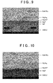
- FIGS. 9 and 10 show the examination results of a semiconductor device of Comparative Example 1.
- Each of FIGS. 7 to 10 shows a SEM image of a joint interface between a solder portion and a metal plate when a semiconductor element was joined to a metal plate.
- Example 1 a Ni layer (NiP) having a thickness of 7.0 ⁇ m as a metal plate was formed on a surface of a Cu plate by electroless-plating the surface of the Cu plate with nickel, and a Cu layer having a thickness of 1.4 ⁇ m was formed by sputtering on a surface of the Ni layer.
- a solder material Sn-0.7Cu solder having a thickness of 0.15 mm was used.
- FIG. 7 shows a joint interface between the solder portion 4a and the Cu plate 2b after arranging the solder material between the semiconductor element and the metal plate, heating the solder material to 230°C, and cooling the solder material to room temperature.
- FIG. 7 shows a joint interface between the solder portion 4a and the Cu plate 2b after arranging the solder material between the semiconductor element and the metal plate, heating the solder material to 230°C, and cooling the solder material to room temperature.
- FIG. 8 shows the joint interface between the solder portion 4a and the Cu plate 2b after performing 4 cycles of a heat treatment in which a step of heating the solder portion 4a of FIG. 7 to 230°C and cooling the solder portion 4a to room temperature was set as one cycle.
- Example 1 a Ni layer (NiP) having a thickness of 7.0 ⁇ m as a metal plate was formed on a surface of a Cu plate by electroless-plating the surface of the Cu plate with nickel.
- a solder material as in the case of Example 1, Sn-0.7Cu solder having a thickness of 0.15 mm was used. That is, Example 1 is different from Comparative Example 1, in that the Cu layer was formed on the surface of the Ni layer.
- FIG. 9 shows a joint interface between a solder portion and the Cu plate 2b after arranging the solder material between the semiconductor element and the metal plate, heating the solder material to 230°C, and cooling the solder material to room temperature.
- FIG. 10 shows the joint interface between the solder portion and the Cu plate 2b after performing 4 cycles of a heat treatment in which a step of heating the solder portion of FIG. 9 to 230°C and cooling the solder portion 4a to room temperature was set as one cycle.
- Example 1 the Cu 6 Sn 5 portion 4b was formed between the Ni layer 2a and the solder portion 4a. As shown in FIG. 8 , even when the heat treatment was repeatedly performed, the Cu 6 Sn 5 portion 4b functioned as a barrier layer so as to prevent Sn of the solder portion from being diffused to the Ni layer 2a.
- Example 1 and Comparative Example 1 since the solder materials were the same (Sn-0.7Cu solder), the melting points of the solder materials were the same. As shown in FIG. 9 , in Comparative Example 1, a Cu 6 Sn 5 layer was not formed between the Ni layer and the solder portion. This result shows that, when the proportion of Cu constituting the solder material is low (0.7 wt%), a Cu 6 Sn 5 layer is not formed. On the other hand, in Example 1, although the solder material was the same as that of Comparative Example 1, the Cu 6 Sn 5 portion 4b was formed between the Ni layer and the solder portion. By forming the copper layer on the surface of the Ni layer, the Cu 6 Sn 5 portion was able to be formed on the surface of the Ni layer without an increase in the temperature during the joining between the semiconductor element and the metal plate.
- the thickness of the Cu layer 22 is adjusted to be 1.4 ⁇ m, and the thickness of the solder material 4 (Sn-0.7Cu solder) is adjusted to be 0.15 mm.
- the total weight of copper is adjusted to be 2.0 wt% with respect to the total weight of the joining materials.
- a Sn solder Sn 100%
- the total weight of copper can be adjusted to be 2.0 wt% with respect to the total weight of the joining materials by adjusting the thickness of the Cu layer to be 2.5 ⁇ m.
- the melting point of the Sn solder is 232°C, which is lower than the liquidus temperature (270°C to 280°C) of Sn-2.0Cu solder.
- the total weight of copper may be higher than 2.0 wt% with respect to the total weight of the joining materials.
- the thickness of the Cu layer may be increased.
- the thickness of the Cu layer can be calculated according to the thickness of the solder material, the proportion of Cu contained in the solder material, and the desired proportion of Cu with respect to the total weight of the joining materials.
- voids are formed between the Cu 6 Sn 5 portion 4b and the Ni layer 2a due to the non-contact portion 18b which is not in contact with the Ni layer 2a.
- copper may be present between the non-contact portion 18b and the Ni layer 2a. Copper may be a residue of the Cu layer 22 provided on the surface of the Ni layer 2a.
- the copper layer 22 is provided on the surface of the Ni layer 2a, and the Ni layer and the copper layer are further provided on the surface of the electrode 6a of the semiconductor element 6. Therefore, a configuration in which Cu 6 Sn 5 was formed on the surface of the Ni layer was obtained in the region (refer to FIG. 1 ) between the electrode 6b and the solder portion 4.
- the sum of the weight of copper contained in the solder material, the weight of copper contained in the copper layer 22, and the weight of copper contained in the copper layer on the surface of the electrode 6a may be 2 wt% or higher with respect to the total weight of the joining materials (including the weight of the copper layer on the surface of the electrode 6a).
- the copper layer 22 may be provided on the surface of the Ni layer 2a only in the metal plate 2 without providing the Ni layer and the copper layer on the surface of the electrode 6a.
- each of the electrodes 6a, 6b of the semiconductor element 6, the metal plates 2, 10, and the spacer 14 includes a Cu portion (Cu plate) and a Ni film which covers a surface of the Cu portion.
- the semiconductor device may have a structure in which at least one of the electrodes 6a, 6b, the metal plates 2, 10, and the spacer 14 includes a Cu portion and a Ni film which covers a surface of the Cu portion.
- the risk of defects in joint portions caused by heat varies depending on the heating conditions and the environmental temperature during the manufacturing steps, the heat generation from the semiconductor element, and the like.
- defects are likely to occur due to heat in the portions that are in direct contact with the semiconductor element 6. That is, in the semiconductor device 100, defects are likely to occur in the joint portion between the metal plate 2 and the semiconductor element 6 and the joint portion between the semiconductor element 6 and the spacer 14. In particular, defects are likely to occur in the joint portion between the semiconductor element 6 and the spacer 14.
- the technique relating to the joining layer (the solder portion containing elemental copper in base metal, and the Cu 6 Sn 5 portion in contact with the nickel layer) disclosed in this specification may be applied to only the above-described portions where defects are likely to occur.
- the semiconductor device may include: a semiconductor element; a joined member on which a Ni layer is provided; and a joining layer through which the joined member is joined.
- the joining layer includes a solder portion and a Cu 6 Sn 5 portion.
- the solder portion may contain at least tin.
- the Cu 6 Sn 5 portion may be provided between the Ni layer and the solder portion.
- a portion of the Cu 6 Sn 5 portion may be in contact with the surface of the Ni layer, and other portions of the Cu 6 Sn 5 portion may not be in contact with the surface of the Ni layer.
- the proportion of Cu contained in the joining layer may be 2.0 wt% or higher.
- the weight of copper contained in the solder portion may be lower than 0.9 wt% with respect to the weight of the solder portion.
- the method of manufacturing a semiconductor device in which the semiconductor element and the joined member are joined to each other includes the arrangement step and the heat treatment step.
- the solder material may be arranged between the semiconductor element and the joined member.
- the Ni layer may be provided on the surface of the joined member, and the copper layer may be provided on at least a portion of the surface of the Ni layer.
- the solder material may contain at least tin.
- the solder material may be in contact with the copper layer.
- the heat treatment step the solder material may be melted and solidified.
- Cu 6 Sn 5 may be formed on the surface of the Ni layer due to tin in the solder material and the copper layer.
- the sum (total weight of copper) of the weight of copper contained in the solder material and the weight of copper in a region in contact with the solder material in the arrangement step may be 2.0 wt% or higher with respect to the sum (total weight of the joining materials) of the weight of the solder material and the weight of copper in the region in contact with the solder material.
- the Ni layer and the copper layer may be formed on the surface of the joined member before the arrangement step.
- the Ni layer may be electroplated on the surface of the joined member.
- the Ni layer may be electroless-plated on the surface of the joined member.
- the Ni layer may be formed by sputtering on the surface of the joined member.
- the copper layer may be electroplated or electroless-plated on the surface of the Ni layer.
- the copper layer may be formed by sputtering on the surface of the Ni layer.
- the material of the solder portion in the joining layer may be the same as the material of the solder material through which the semiconductor element and the joined member are joined to each other.
- the proportion of tin in the solder material may be 100% (tin solder).
- the solder material may be Sn-Cu solder containing copper.
- the proportion of copper constituting the solder material may be 0.3 wt% or higher and is preferably 0.5 wt% or higher. It is more preferable that the solder material is Sn-0.7Cu (Cu content ratio: 0.7%).
- an ⁇ (eta) phase compound (Cu 6 Sn 5 ) is formed during phase transformation from the liquid phase to the solid phase.
- the proportion of copper contained in the Sn-Cu solder is adjusted to be 0.3 wt% or higher. As a result, even when there is a variation in the thickness of the copper layer provided on the Ni layer, the Cu 6 Sn 5 portion can be reliably formed. By adjusting the proportion of copper to be 0.5 wt% or higher, the Cu 6 Sn 5 portion can be more reliably formed.
- Sn-0.7Cu solder has the lowest melting point.
- solder material is Sn0.7Cu solder (Cu content ratio: 0.7%).
- Sn-Cu solder is a general term for alloys containing tin and copper as major components and may further contain, for example, Ni, P (phosphorus), Bi (bismuth), Sb (antimony), or Ag (silver) in addition to tin and copper.
- the proportion of copper constituting the solder material may be 7.6 wt% or lower and is preferably 5.0 wt% or lower and more preferably 4.0 wt% or lower.
- an ⁇ (epsilon) phase compound Cu 3 Sn
- an ⁇ (eta) phase compound Cu 6 Sn 5
- the proportion of the total weight of copper is higher than 7.6 wt% with respect to the total weight of the joining materials, not Cu 6 Sn 5 but Cu 3 Sn is formed.
- the proportion of the total weight of copper is preferably lower than 7.6 wt%.
- the Sn-Cu solder (Sn-5.0Cu solder) in which the proportion of copper constituting the solder material is 5.0 wt% has a melting point of 350°C.
- An element protective film used for a semiconductor element may deteriorate at a temperature higher than 350°C. Therefore, when the proportion of copper constituting the solder material is higher than 5.0 wt%, it is necessary to take countermeasures to suppress deterioration of the element protective film.
- the proportion of copper constituting the solder material By adjusting the proportion of copper constituting the solder material to be 5.0 wt% or lower, deterioration of the element protective film can be suppressed without taking any special countermeasures.
- the Sn-Cu solder (Sn-4.0Cu solder) in which the proportion of copper constituting the solder material is 4.0 wt% has a melting point of 330°C.
- An electrode used in a semiconductor element may crack at a temperature of higher than 330°C depending on the material thereof. Therefore, when the proportion of copper constituting the solder material is higher than 4.0 wt%, it is necessary to take countermeasures for preventing the cracking of an electrode. For example, it is necessary to limit the material of an electrode.
- the proportion of copper constituting the solder material By adjusting the proportion of copper constituting the solder material to be 4.0 wt% or lower, a semiconductor device in which the cracking of an electrode is suppressed can be obtained without taking any special countermeasures.
- the total weight of copper may be 2.0 wt% or higher and is more preferably 3.0 wt% or higher with respect to the total weight of the joining materials.
- an ⁇ (eta) phase compound (Cu 6 Sn 5 ) is formed during phase transformation from the liquid phase to the solid phase. That is, by adjusting the total weight of copper to be 2.0 wt% or higher, the Cu 6 Sn 5 portion can be reliably formed on the surface of the Ni layer. By adjusting the total weight of copper to be 3.0 wt% or higher, the Cu 6 Sn 5 portion can be more stably formed on the surface of the Ni layer.
- the thickness of the copper layer (weight of the copper layer) may be adjusted according to the proportion of Cu contained in the solder material.
- a method of manufacturing a semiconductor device (100) includes: arranging a solder material (4) containing at least tin, between a semiconductor element (6) and a joined member (2) provided with a nickel layer (2a) and a copper layer (22), such that the solder material is in contact with the copper layer, the nickel layer being provided on a surface of the joined member, and the copper layer being provided on at least a portion of a surface of the nickel layer; and melting and solidifying the solder material to form Cu 6 Sn 5 on the surface of the nickel layer using tin of the solder material and the copper layer.
Landscapes
- Engineering & Computer Science (AREA)
- Mechanical Engineering (AREA)
- Chemical & Material Sciences (AREA)
- Materials Engineering (AREA)
- Metallurgy (AREA)
- Organic Chemistry (AREA)
- Die Bonding (AREA)
- Lead Frames For Integrated Circuits (AREA)
Abstract

Description
- The present invention relates to a semiconductor device and a method of manufacturing a semiconductor device. In particular, the invention relates to a semiconductor device in which an electrode of a semiconductor element is joined to a joined member.
-
Japanese Patent Application Publication No. 2007-67158 JP 2007-67158 A JP 2007-67158 A JP 2007-67158 A - As described in
JP 2007-67158 A JP 2007-67158 A - However, when the proportion of Cu constituting a Sn-Cu solder increases, the melting point (or liquidus temperature) of the solder increases. For example, in the case of Sn-3.0Cu solder, the liquidus temperature is higher than 310°C. When a solder having a high melting point (liquidus temperature) is used, it is necessary that the heat resistance of a semiconductor element is improved to prevent the semiconductor element from being damaged. Therefore, a method of manufacturing a semiconductor device is provided which is capable of suppressing the melting point (or liquidus temperature) of a solder to be low while achieving the formation of a Cu6Sn5 compound on a surface of a joined member. Further, a semiconductor device is also provided.
- According to a first aspect of the invention, there is provided a method of manufacturing a semiconductor device including: arranging a solder material containing at least tin, between a semiconductor element and a joined member provided with a nickel layer and a copper layer, such that the solder material is in contact with the copper layer, the nickel layer being provided on a surface of the joined member, and the copper layer being provided on at least a portion of a surface of the nickel layer; and melting and solidifying the solder material to form Cu6Sn5 on the surface of the nickel layer using tin of the solder material and the copper layer.
- "Solder material" described in this specification refers to a material before melting and, when melted, is used to join a semiconductor element and a joined member to each other. On the other hand, a portion of the joining layer through which the semiconductor element and the joined member are joined to each other, which is a material after joining the semiconductor element and the joined member to each other (that is, after the solidification of the solder material), is called "solder portion" and is distinguished from the solder material. "Copper in contact with the solder material" is not limited to copper in the copper layer provided on the surface of the nickel layer. "Copper in contact with the solder material" includes copper of a region other than the surface of the nickel layer (for example, a surface of an electrode of the semiconductor element) as long as it comes into contact with the solder material during the arrangement step. In addition, "Cu6Sn5 portion (or Cu6Sn5)" includes a compound in which a part of Cu is substituted with Ni. That is, "Cu6Sn5 portion (or Cu6Sn5)" includes (Cu,Ni)6Sn5. For example, when a Sn-Cu solder to which Ni is added is used, Ni forms a solid solution in Cu6Sn5 to form (Cu,Ni)6Sn5. Cu6Sn5 and (Cu,Ni)6Sn5 exhibit substantially the same function. The joined member is not limited to a member that is directly joined to the semiconductor element, and includes a member (second member) that is joined to a member (first member) joined to the semiconductor element. That is, the joined member described in this specification refers to a member that is directly or indirectly joined to the semiconductor element. When the first member and the second member are joined to each other using the above-described method, practically, the solder material is arranged between the first member and the second member. The arrangement step of arranging the solder material between the semiconductor element and the joined member includes arranging the solder material between the first member, which is joined to the semiconductor element, and the second member.
- In the above-described manufacturing method, the solder material is melted and solidified in a state where the solder material and the copper layer are in contact with each other. The copper layer in contact with the solder material may be a Cu component for forming the Cu6Sn5 portion when the solder material is melted and then solidified to join the semiconductor element to the joined member. Therefore, even when the proportion of Cu contained in the solder material is low, the Cu6Sn5 portion can be obtained. By suppressing the proportion of Cu contained in the solder material to be low, the melting point (or liquidus temperature) of the solder material can be reduced. The Cu6Sn5 portion is deposited on the surface of the nickel layer. According to the above-described manufacturing method, even when a solder material (having a low copper content and a low melting point or liquidus temperature) which is theoretically incapable of forming Cu6Sn5 is used, the Cu6Sn5 portion can be formed on the surface of the nickel layer. That is, a solder material having a low melting point (or liquidus temperature) can be used while achieving the formation of the Cu6Sn5 compound on the surface of the joined member. In addition, in the above-described manufacturing method, when the semiconductor element and the joined member are joined to each other, exposure of the semiconductor element to a high temperature can be suppressed. Therefore, high heat resistance is not required for the semiconductor element.
- According to a second aspect of the invention, there is provided a semiconductor device including: a semiconductor element; a joined member on which a nickel layer is provided; and a joining layer through which the joined member is joined to the semiconductor element, in which the joining layer includes a solder portion and a Cu6Sn5 portion, the solder portion containing at least tin, and the Cu6Sn5 portion being provided between the nickel layer and the solder portion, the Cu6Sn5 portion is in contact with a portion of a surface of the nickel layer and is not in contact with other portions of the surface of the nickel layer, and a proportion of copper contained in the joining layer is 2.0 wt% or higher.
- According to a third aspect of the invention, there is provided a semiconductor device including: a semiconductor element; a joined member on which a nickel layer is provided; and a joining layer through which the joined member is joined to the semiconductor element, in which the joining layer includes a solder portion and a Cu6Sn5 portion, the solder portion containing tin and copper, and the Cu6Sn5 portion being provided between the nickel layer and the solder portion, and the weight of copper contained in the solder portion is lower than 0.9 wt% with respect to the weight of the solder portion.
- Features, advantages, and technical and industrial significance of exemplary embodiments of the invention will be described below with reference to the accompanying drawings, in which like numerals denote like elements, and wherein:
-
FIG. 1 is a schematic diagram showing a semiconductor device; -
FIG. 2 is an enlarged view showing a portion ofFIG. 1 surrounded by broken lines; -
FIG. 3 is a diagram showing characteristics of a joint interface between a nickel layer and a Cu6Sn5 portion; -
FIG. 4 is a diagram showing a method of manufacturing a semiconductor device; -
FIG. 5 is a Cu-Sn binary phase diagram; -
FIG. 6 is an enlarged view showing a part (Sn: 80 to 100) ofFIG. 5 ; -
FIG. 7 is a SEM image showing a joint interface between a semiconductor element and a joined member in a semiconductor device of Example 1; -
FIG. 8 is a SEM image showing the joint interface between the semiconductor element and the joined member after the semiconductor device of Example 1 was repeatedly heated; -
FIG. 9 is a SEM image showing a joint interface between a semiconductor element and a joined member in a semiconductor device of Comparative Example 1; and -
FIG. 10 is a SEM image showing the joint interface between the semiconductor element and the joined member after the semiconductor device of Comparative Example 1 was repeatedly heated. - Referring to
FIG. 1 , asemiconductor device 100 will be described. In thesemiconductor device 100, asemiconductor element 6 is arranged between twometal plates resin 8. Themetal plates semiconductor device 100. In addition, themetal plates semiconductor element 6 to the outside of thesemiconductor device 100. One surface of each of themetal plates resin 8. InFIG. 1 , terminals, bonding wires, and the like connected to thesemiconductor element 6 are not shown. - A joining
layer 4 is provided between thesemiconductor element 6 and themetal plate 2. More specifically, anelectrode 6a provided on themetal plate 2 side (hereinafter, referred to as "back surface") of thesemiconductor element 6 is soldered to themetal plate 2. In addition, anelectrode 6b provided on themetal plate 10 side (hereinafter, referred to as "front surface") of thesemiconductor element 6 is soldered to a back surface of ametal spacer 14. A front surface of thespacer 14 is soldered to a back surface of themetal plate 10. That is, thesemiconductor element 6 is joined to themetal plate 2 through the joininglayer 4, thesemiconductor element 6 is joined to thespacer 14 through a joininglayer 16, and thespacer 14 is joined to themetal plate 10 through a joininglayer 12. It can be said that themetal plate 10 is indirectly joined to thesemiconductor element 6. Themetal plates spacer 14 are examples of the joined member. - Surfaces of the
semiconductor element 6, themetal plates spacer 14, and the joininglayers resin 8; and thesemiconductor element 6, themetal plates spacer 14, and the joininglayers resin 8. -
FIG. 2 schematically shows an interface between themetal plate 2 and the joininglayer 4. As shown inFIG. 2 , themetal plate 2 includes aCu plate 2b and aNi layer 2a. TheNi layer 2a covers the surface of theCu plate 2b. The thickness of theNi layer 2a is adjusted to be 2 µm to 20 µm. The joininglayer 4 includes asolder portion 4a and a Cu6Sn5 portion 4b. The Cu6Sn5 portion 4b separates thesolder portion 4a and theNi layer 2a from each other. The Cu6Sn5 portion 4b prevents contact between thesolder portion 4a and theNi layer 2a. As shown inFIG. 3 , the Cu6Sn5 portion 4b includes: acontact portion 18a that is in contact with asurface 20 of theNi layer 2a; and anon-contact portion 18b that is not in contact with thesurface 20 of theNi layer 2a. A space between thesurface 20 and thenon-contact portion 18b is hollow. In other words, voids are present in a part of the space between the Cu6Sn5 portion 4b and theNi layer 2a. A Cu portion and a Ni film which covers a surface of the Cu portion are also provided on a surface of theelectrode 6a. Therefore, an interface between theelectrode 6a and the joininglayer 4 also has the same configuration as the interface between themetal plate 2 and the joininglayer 4. - Referring to
FIG. 4 , a step of joining thesemiconductor element 6 to themetal plate 2 will be described. First, theNi layer 2a is formed on the surface of theCu plate 2b. As a result, themetal plate 2 on which theNi layer 2a is provided is obtained. Next, aCu layer 22 is formed at a predetermined position on a surface of theNi layer 2a. Next, asolder material 4 is arranged between theback surface electrode 6a of thesemiconductor element 6 and the Cu layer 22 (arrangement step). At this time, thesolder material 4 is arranged so as to be in contact with theCu layer 22. The solder material is arranged on the entire region of the surface of theCu layer 22. Thesolder material 4 is Sn-0.7Cu solder, and the thickness thereof is adjusted to be 0.15 mm. The thickness of theCu layer 22 is adjusted to be 1.4 µm, and the weight of theCu layer 22 is 1.3 wt% with respect to the sum of the weight of thesolder material 4 and the weight of the Cu layer 22 (total weight of the joining materials). That is, the sum of the weight of copper contained in thesolder material 4 and the weight of the Cu layer 22 (total weight of copper) is 2.0 wt% with respect to the total weight of the joining materials. - A Cu layer may be formed on the entire region of the surface of the
Ni layer 2a, and thesolder material 4 may be arranged at a predetermined position on a surface of the Cu layer (at a portion of the surface of the Cu layer). In this case, when the thickness of the Cu layer is adjusted to be 1.4 µm, the weight of the Cu layer is greater than that in the above-described embodiment in which the Cu layer is provided at the predetermined position. However, the total weight of copper refers to the sum of the weight of copper contained in thesolder material 4 and the weight of the Cu layer in a region in contact with thesolder material 4. In addition, the total weight of the joining materials refers to the sum of the weight of thesolder material 4 and the weight of the Cu layer in a region in contact with thesolder material 4. Therefore, even when a Cu layer is formed on the entire region of the surface of theNi layer 2a, and when thesolder material 4 is arranged at a predetermined position on a surface of the Cu layer, the total weight of copper is adjusted to be 1.3 wt% with respect to the total weight of the joining materials by adjusting the thickness of the Sn-0.7Cu solder (solder material) to be 0.15 mm and adjusting the thickness of the Cu layer to be 1.4 µm. That is, the weight of the Cu layer in a region not in contact with thesolder material 4 is not included in the total weight of the joining materials and the total weight of copper. - Next, a heat treatment is performed on the
solder material 4 at 230°C, and thesolder material 4 is melted and solidified (heat treatment step). When thesolder material 4 is solidified, Cu of theCu layer 22 reacts with thesolder material 4 to form Cu6Sn5. As a result, as shown inFIG. 2 , the Cu6Sn5 portion 4b is deposited on the surface of theNi layer 2a. In the related art, even when themetal plate 2 and thesemiconductor element 6 are joined to each other through the Sn-0.7Cu solder, Cu6Sn5 is not deposited on the surface of theNi layer 2a. On the other hand, in the embodiment, theCu layer 22 is formed on the surface of theNi layer 2a, and thesolder material 4 is melted and solidified in a state where thesolder material 4 is in contact with theCu layer 22. TheCu layer 22 may be the Cu6Sn5 material. Accordingly, although the solder material (Sn-0.7Cu solder) having a low proportion of Cu is used, the Cu6Sn5 portion 4b can be formed during the solidification of the solder material. As described above, the total weight of copper is 2.0 wt% with respect to the total weight of the joining materials. When the total weight of copper is 2.0 wt% with respect to the total weight of the joining materials, the Cu6Sn5 portion 4b can be reliably formed. - In the embodiment, the entire region of the
Cu layer 22 is removed by joining thesemiconductor element 6 to themetal plate 2. Therefore, as shown inFIG. 3 , a configuration in which theNi layer 2a and the Cu6Sn5 portion 4b are in direct contact with each other is obtained. By removing the entire region of theCu layer 22, theNi layer 2a and the Cu6Sn5 portion 4b are partially not in contact with each other. That is, the Cu6Sn5 portion 4b includes: thecontact portion 18a that is in contact with theNi layer 2a; and thenon-contact portion 18b that is not in contact with theNi layer 2a. In thenon-contact portion 18b, voids are formed between the Cu6Sn5 portion 4b and theNi layer 2a. However, the voids are surrounded by theNi layer 2a and the Cu6Sn5 portion 4b and are not connected to thesolder portion 4a. Therefore, mutual diffusion between thesolder portion 4a and theNi layer 2a is prevented. - As described above, by providing the
Cu layer 22 on the surface of theNi layer 2a, the proportion of Cu contained in thesolder material 4 as an alloy is suppressed to be low at 0.7 wt%. By suppressing the proportion of Cu contained in the solder material, the melting point (or liquidus temperature) of the solder material can be reduced. As shown inFIGS. 5 and6 , the melting point of the Sn-0.7Cu solder is 227°C, which is lower than the liquidus temperature of a Sn-2.0Cu solder (270°C to 280°C). In the method according to the embodiment, when thesemiconductor element 6 and themetal plate 2 are joined to each other, without providing theCu layer 22, the temperature applied to thesemiconductor element 6 can be reduced to be lower than that of a case where Sn-2.0Cu solder is used for the joining. Therefore, with the method according to the embodiment, the temperature applied to thesemiconductor element 6 in the soldering step can be reduced. - As in the
metal plate 2, in themetal plate 10, Ni is electroplated on the surface of the Cu plate. In thespacer 14, Ni is electroplated on both surfaces (front surface and back surface) of the Cu plate. In addition, a Ni film is formed on the surface of theelectrode 6b. The joint portion between theelectrode 6b and thespacer 14 and the joint portion between thespacer 14 and themetal plate 10 have substantially the same structure as the joint portion between thesemiconductor element 6 and themetal plate 2. Therefore, the description of the interface between thesemiconductor element 6 and the joininglayer 16, the interface between thespacer 14 and the joininglayer 16, the interface between thespacer 14 and the joininglayer 12, and the interface between themetal plate 10 and the joininglayer 12 will be replaced with the description of the interface between themetal plate 2 and the joininglayer 4. - The advantageous effects of the
semiconductor device 100 will be described. As described above, the Cu6Sn5 portion 4b is provided between thesolder portion 4a and theNi layer 2a. Therefore, the Cu6Sn5 portion 4b functions as a barrier layer. Therefore, even when heat is generated from thesemiconductor element 6, mutual diffusion between tin of thesolder portion 4a and nickel of theNi layer 2a can be suppressed. By the Cu6Sn5 portion 4b being provided, the formation of a compound of tin and nickel on the interface between thesemiconductor element 6 and themetal plate 2 can be suppressed. By forming a compound of tin and nickel on the interface between thesemiconductor element 6 and themetal plate 2, the semiconductor device is heated and cooled. Accordingly, the modification of theNi layer 2a progresses. When the modification of theNi layer 2a reaches theCu plate 2b, themetal plate 2 may be peeled off from thesemiconductor element 6. Since the Cu6Sn5 portion 4b is present between thesolder portion 4a and theNi layer 2a, such peeling can be prevented. Further, in thesemiconductor device 100, theCu layer 22 is provided on the surface of theNi layer 2a. As a result, the Cu6Sn5 portion 4b can be formed using the solder material having a low proportion of Cu. Therefore, the temperature applied to thesemiconductor element 6 in the soldering step can be reduced. - Referring to
FIGS. 7 to 10 , characteristics of a semiconductor device of Example 1 will be described.FIGS. 7 and 8 show the examination results of the semiconductor device of Example 1.FIGS. 9 and 10 show the examination results of a semiconductor device of Comparative Example 1. Each ofFIGS. 7 to 10 shows a SEM image of a joint interface between a solder portion and a metal plate when a semiconductor element was joined to a metal plate. - In Example 1, a Ni layer (NiP) having a thickness of 7.0 µm as a metal plate was formed on a surface of a Cu plate by electroless-plating the surface of the Cu plate with nickel, and a Cu layer having a thickness of 1.4 µm was formed by sputtering on a surface of the Ni layer. As a solder material, Sn-0.7Cu solder having a thickness of 0.15 mm was used.
FIG. 7 shows a joint interface between thesolder portion 4a and theCu plate 2b after arranging the solder material between the semiconductor element and the metal plate, heating the solder material to 230°C, and cooling the solder material to room temperature.FIG. 8 shows the joint interface between thesolder portion 4a and theCu plate 2b after performing 4 cycles of a heat treatment in which a step of heating thesolder portion 4a ofFIG. 7 to 230°C and cooling thesolder portion 4a to room temperature was set as one cycle. - In Comparative Example 1, a Ni layer (NiP) having a thickness of 7.0 µm as a metal plate was formed on a surface of a Cu plate by electroless-plating the surface of the Cu plate with nickel. As a solder material, as in the case of Example 1, Sn-0.7Cu solder having a thickness of 0.15 mm was used. That is, Example 1 is different from Comparative Example 1, in that the Cu layer was formed on the surface of the Ni layer.
FIG. 9 shows a joint interface between a solder portion and theCu plate 2b after arranging the solder material between the semiconductor element and the metal plate, heating the solder material to 230°C, and cooling the solder material to room temperature.FIG. 10 shows the joint interface between the solder portion and theCu plate 2b after performing 4 cycles of a heat treatment in which a step of heating the solder portion ofFIG. 9 to 230°C and cooling thesolder portion 4a to room temperature was set as one cycle. - As shown in
FIG. 7 , in Example 1, the Cu6Sn5 portion 4b was formed between theNi layer 2a and thesolder portion 4a. As shown inFIG. 8 , even when the heat treatment was repeatedly performed, the Cu6Sn5 portion 4b functioned as a barrier layer so as to prevent Sn of the solder portion from being diffused to theNi layer 2a. - On the other hand, as shown in
FIG. 9 , in Comparative Example 1, not the Cu6Sn5 portion 4b but a Ni3Sn4 layer and a Ni3SnP layer were formed between theNi layer 2a and thesolder portion 4a. Ni3P was modified on the surface of the Ni layer (NiP). Further, as shown inFIG. 10 , when the heat treatment was repeatedly performed four times, Ni3P grew, and substantially the entire region of the Ni layer (NiP) was modified to Ni3P. When Ni3P reaches theCu plate 2b, theCu plate 2b may be peeled off from thesolder portion 4a. - In Example 1 and Comparative Example 1, since the solder materials were the same (Sn-0.7Cu solder), the melting points of the solder materials were the same. As shown in
FIG. 9 , in Comparative Example 1, a Cu6Sn5 layer was not formed between the Ni layer and the solder portion. This result shows that, when the proportion of Cu constituting the solder material is low (0.7 wt%), a Cu6Sn5 layer is not formed. On the other hand, in Example 1, although the solder material was the same as that of Comparative Example 1, the Cu6Sn5 portion 4b was formed between the Ni layer and the solder portion. By forming the copper layer on the surface of the Ni layer, the Cu6Sn5 portion was able to be formed on the surface of the Ni layer without an increase in the temperature during the joining between the semiconductor element and the metal plate. - In the above-described embodiment, the thickness of the
Cu layer 22 is adjusted to be 1.4 µm, and the thickness of the solder material 4 (Sn-0.7Cu solder) is adjusted to be 0.15 mm. As a result, the total weight of copper is adjusted to be 2.0 wt% with respect to the total weight of the joining materials. However, for example, a Sn solder (Sn 100%) may be used as a solder material. When a Sn solder is used, the total weight of copper can be adjusted to be 2.0 wt% with respect to the total weight of the joining materials by adjusting the thickness of the Cu layer to be 2.5 µm. In this case, the melting point of the Sn solder is 232°C, which is lower than the liquidus temperature (270°C to 280°C) of Sn-2.0Cu solder. The total weight of copper may be higher than 2.0 wt% with respect to the total weight of the joining materials. In this case, the thickness of the Cu layer may be increased. The thickness of the Cu layer can be calculated according to the thickness of the solder material, the proportion of Cu contained in the solder material, and the desired proportion of Cu with respect to the total weight of the joining materials. - In the above-described embodiment, voids are formed between the Cu6Sn5 portion 4b and the
Ni layer 2a due to thenon-contact portion 18b which is not in contact with theNi layer 2a. However, copper may be present between thenon-contact portion 18b and theNi layer 2a. Copper may be a residue of theCu layer 22 provided on the surface of theNi layer 2a. - In the above-described embodiment, the
copper layer 22 is provided on the surface of theNi layer 2a, and the Ni layer and the copper layer are further provided on the surface of theelectrode 6a of thesemiconductor element 6. Therefore, a configuration in which Cu6Sn5 was formed on the surface of the Ni layer was obtained in the region (refer toFIG. 1 ) between theelectrode 6b and thesolder portion 4. In this case, the sum of the weight of copper contained in the solder material, the weight of copper contained in thecopper layer 22, and the weight of copper contained in the copper layer on the surface of theelectrode 6a may be 2 wt% or higher with respect to the total weight of the joining materials (including the weight of the copper layer on the surface of theelectrode 6a). Thecopper layer 22 may be provided on the surface of theNi layer 2a only in themetal plate 2 without providing the Ni layer and the copper layer on the surface of theelectrode 6a. - Similarly, in the description of the above-described embodiment, in the semiconductor device, each of the
electrodes semiconductor element 6, themetal plates spacer 14 includes a Cu portion (Cu plate) and a Ni film which covers a surface of the Cu portion. However, the semiconductor device may have a structure in which at least one of theelectrodes metal plates spacer 14 includes a Cu portion and a Ni film which covers a surface of the Cu portion. In a semiconductor device, the risk of defects in joint portions caused by heat varies depending on the heating conditions and the environmental temperature during the manufacturing steps, the heat generation from the semiconductor element, and the like. In thesemiconductor device 100, defects are likely to occur due to heat in the portions that are in direct contact with thesemiconductor element 6. That is, in thesemiconductor device 100, defects are likely to occur in the joint portion between themetal plate 2 and thesemiconductor element 6 and the joint portion between thesemiconductor element 6 and thespacer 14. In particular, defects are likely to occur in the joint portion between thesemiconductor element 6 and thespacer 14. The technique relating to the joining layer (the solder portion containing elemental copper in base metal, and the Cu6Sn5 portion in contact with the nickel layer) disclosed in this specification may be applied to only the above-described portions where defects are likely to occur. - Some technical characteristics of the semiconductor device and the method of manufacturing a semiconductor device disclosed in this specification will be described. The following features have individual technical significance.
- The semiconductor device may include: a semiconductor element; a joined member on which a Ni layer is provided; and a joining layer through which the joined member is joined. The joining layer includes a solder portion and a Cu6Sn5 portion. The solder portion may contain at least tin. The Cu6Sn5 portion may be provided between the Ni layer and the solder portion. A portion of the Cu6Sn5 portion may be in contact with the surface of the Ni layer, and other portions of the Cu6Sn5 portion may not be in contact with the surface of the Ni layer. The proportion of Cu contained in the joining layer may be 2.0 wt% or higher. The weight of copper contained in the solder portion may be lower than 0.9 wt% with respect to the weight of the solder portion.
- The method of manufacturing a semiconductor device in which the semiconductor element and the joined member are joined to each other includes the arrangement step and the heat treatment step. In the arrangement step, the solder material may be arranged between the semiconductor element and the joined member. The Ni layer may be provided on the surface of the joined member, and the copper layer may be provided on at least a portion of the surface of the Ni layer. The solder material may contain at least tin. In the arrangement step, the solder material may be in contact with the copper layer. In the heat treatment step, the solder material may be melted and solidified. In the heat treatment step, Cu6Sn5 may be formed on the surface of the Ni layer due to tin in the solder material and the copper layer. The sum (total weight of copper) of the weight of copper contained in the solder material and the weight of copper in a region in contact with the solder material in the arrangement step may be 2.0 wt% or higher with respect to the sum (total weight of the joining materials) of the weight of the solder material and the weight of copper in the region in contact with the solder material.
- The Ni layer and the copper layer may be formed on the surface of the joined member before the arrangement step. The Ni layer may be electroplated on the surface of the joined member. Alternatively, the Ni layer may be electroless-plated on the surface of the joined member. The Ni layer may be formed by sputtering on the surface of the joined member. Similarly, the copper layer may be electroplated or electroless-plated on the surface of the Ni layer. The copper layer may be formed by sputtering on the surface of the Ni layer.
- The material of the solder portion in the joining layer may be the same as the material of the solder material through which the semiconductor element and the joined member are joined to each other. The proportion of tin in the solder material may be 100% (tin solder). The solder material may be Sn-Cu solder containing copper. When the solder material is Sn-Cu solder, the proportion of copper constituting the solder material may be 0.3 wt% or higher and is preferably 0.5 wt% or higher. It is more preferable that the solder material is Sn-0.7Cu (Cu content ratio: 0.7%). As clearly seen from
FIGS. 5 and6 , in Sn-0.3Cu solder, Sn-0.5Cu solder, and Sn-0.7Cu solder, an η (eta) phase compound (Cu6Sn5) is formed during phase transformation from the liquid phase to the solid phase. The proportion of copper contained in the Sn-Cu solder is adjusted to be 0.3 wt% or higher. As a result, even when there is a variation in the thickness of the copper layer provided on the Ni layer, the Cu6Sn5 portion can be reliably formed. By adjusting the proportion of copper to be 0.5 wt% or higher, the Cu6Sn5 portion can be more reliably formed. Among the Sn-Cu solders, Sn-0.7Cu solder has the lowest melting point. From the viewpoint of suppressing exposure of the semiconductor element to a high temperature in the joining step, it is more preferable the solder material is Sn0.7Cu solder (Cu content ratio: 0.7%). In addition, "Sn-Cu solder" is a general term for alloys containing tin and copper as major components and may further contain, for example, Ni, P (phosphorus), Bi (bismuth), Sb (antimony), or Ag (silver) in addition to tin and copper. - The proportion of copper constituting the solder material may be 7.6 wt% or lower and is preferably 5.0 wt% or lower and more preferably 4.0 wt% or lower. As shown in
FIGS. 5 and6 , when the Cu content ratio in the Sn-Cu solder is higher than 7.6 wt%, an ε (epsilon) phase compound (Cu3Sn) is formed during phase transformation of the base metal from the liquid phase to the solid phase. On the other hand, when the Cu content ratio is 7.6 wt% or lower, an η (eta) phase compound (Cu6Sn5) is formed during phase transformation of the base metal from the liquid phase to the solid phase. Therefore, when the total weight of copper is higher than 7.6 wt% with respect to the total weight of the joining materials, not Cu6Sn5 but Cu3Sn is formed. By adjusting the proportion of the total weight of copper to be 7.6 wt% or lower, the Cu6Sn5 portion can be reliably formed. From the viewpoint of providing the copper layer on the surface of the Ni layer and reliably forming the Cu6Sn5 portion, the proportion of copper constituting the solder material is preferably lower than 7.6 wt%. - As shown in
FIG. 6 , the Sn-Cu solder (Sn-5.0Cu solder) in which the proportion of copper constituting the solder material is 5.0 wt% has a melting point of 350°C. An element protective film used for a semiconductor element may deteriorate at a temperature higher than 350°C. Therefore, when the proportion of copper constituting the solder material is higher than 5.0 wt%, it is necessary to take countermeasures to suppress deterioration of the element protective film. By adjusting the proportion of copper constituting the solder material to be 5.0 wt% or lower, deterioration of the element protective film can be suppressed without taking any special countermeasures. - As shown in
FIG. 6 , the Sn-Cu solder (Sn-4.0Cu solder) in which the proportion of copper constituting the solder material is 4.0 wt% has a melting point of 330°C. An electrode used in a semiconductor element may crack at a temperature of higher than 330°C depending on the material thereof. Therefore, when the proportion of copper constituting the solder material is higher than 4.0 wt%, it is necessary to take countermeasures for preventing the cracking of an electrode. For example, it is necessary to limit the material of an electrode. By adjusting the proportion of copper constituting the solder material to be 4.0 wt% or lower, a semiconductor device in which the cracking of an electrode is suppressed can be obtained without taking any special countermeasures. - The total weight of copper may be 2.0 wt% or higher and is more preferably 3.0 wt% or higher with respect to the total weight of the joining materials. As clearly seen from
FIGS. 5 and6 , in Sn-2.0Cu solder, an η (eta) phase compound (Cu6Sn5) is formed during phase transformation from the liquid phase to the solid phase. That is, by adjusting the total weight of copper to be 2.0 wt% or higher, the Cu6Sn5 portion can be reliably formed on the surface of the Ni layer. By adjusting the total weight of copper to be 3.0 wt% or higher, the Cu6Sn5 portion can be more stably formed on the surface of the Ni layer. The thickness of the copper layer (weight of the copper layer) may be adjusted according to the proportion of Cu contained in the solder material. - Hereinabove, specific examples of the invention have been described in detail. However, these examples are merely exemplary and do not limit the claims. The technique described in the claims includes various modifications and alternations of the above-described specific examples. The technical features described in this specification and the drawings exhibit technical significance when being used alone or in a combination thereof, and are not limited to the combinations described in the claims at the time of filing of the application. The technique exemplified in this specification or the drawings simultaneously achieves plural objects, and the technical significance is obtained by achieving one of the objects.
- A method of manufacturing a semiconductor device (100) includes: arranging a solder material (4) containing at least tin, between a semiconductor element (6) and a joined member (2) provided with a nickel layer (2a) and a copper layer (22), such that the solder material is in contact with the copper layer, the nickel layer being provided on a surface of the joined member, and the copper layer being provided on at least a portion of a surface of the nickel layer; and melting and solidifying the solder material to form Cu6Sn5 on the surface of the nickel layer using tin of the solder material and the copper layer.
Claims (7)
- A method of manufacturing a semiconductor device (100) characterized by comprising:arranging a solder material (4) containing at least tin, between a semiconductor element (6) and a joined member (2b) provided with a nickel layer (2a) and a copper layer (22), such that the solder material is in contact with the copper layer, the nickel layer being provided on a surface of the joined member, and the copper layer being provided on at least a portion of a surface of the nickel layer; andmelting and solidifying the solder material to form Cu6Sn5 on the surface of the nickel layer using tin of the solder material and the copper layer.
- The method of manufacturing a semiconductor device according to claim 1, characterized in that
a sum of the weight of copper contained in the solder material and the weight of copper in a region in contact with the solder material is 2.0 wt% or higher with respect to a sum of the weight of the solder material and the weight of copper in the region in contact with the solder material. - The method of manufacturing a semiconductor device according to claim 1 or 2 characterized in that
a sum of the weight of copper contained in the solder material and the weight of copper in a region in contact with the solder material is 7.6 wt% or lower with respect to a sum of the weight of the solder material and the weight of copper in the region in contact with the solder material. - The method of manufacturing a semiconductor device according to any one of claims 1 to 3 characterized in that
the solder material contains copper. - The method of manufacturing a semiconductor device according to claim 4, characterized in that
the solder material is an alloy containing Sn-0.7Cu as a major component. - A semiconductor device characterized by comprising:a semiconductor element;a joined member on which a nickel layer is provided; anda joining layer through which the joined member is joined to the semiconductor element, whereinthe joining layer includes a solder portion and a Cu6Sn5 portion, the solder portion containing at least tin, and the Cu6Sn5 portion being provided between the nickel layer and the solder portion,the Cu6Sn5 portion is in contact with a portion of a surface of the nickel layer and is not in contact with other portions of the surface of the nickel layer, anda proportion of copper contained in the joining layer is 2.0 wt% or higher.
- A semiconductor device characterized by comprising:a semiconductor element;a joined member on which a nickel layer is provided; anda joining layer through which the joined member is joined to the semiconductor element, whereinthe joining layer includes a solder portion and a Cu6Sn5 portion, the solder portion containing tin and copper, and the Cu6Sn5 portion being provided between the nickel layer and the solder portion, andthe weight of copper contained in the solder portion is lower than 0.9 wt% with respect to the weight of the solder portion.
Applications Claiming Priority (1)
| Application Number | Priority Date | Filing Date | Title |
|---|---|---|---|
| JP2014221353A JP6281468B2 (en) | 2014-10-30 | 2014-10-30 | Semiconductor device and manufacturing method thereof |
Publications (1)
| Publication Number | Publication Date |
|---|---|
| EP3021357A1 true EP3021357A1 (en) | 2016-05-18 |
Family
ID=54364136
Family Applications (1)
| Application Number | Title | Priority Date | Filing Date |
|---|---|---|---|
| EP15192112.9A Ceased EP3021357A1 (en) | 2014-10-30 | 2015-10-29 | Method of joining a semiconductor element to a joined member by reacting a tin-containing solder material with a copper layer on the joined member and corresponding semiconductor device |
Country Status (7)
| Country | Link |
|---|---|
| US (1) | US9659892B2 (en) |
| EP (1) | EP3021357A1 (en) |
| JP (1) | JP6281468B2 (en) |
| KR (1) | KR101740819B1 (en) |
| CN (1) | CN105575830B (en) |
| BR (1) | BR102015027638B1 (en) |
| TW (1) | TWI627686B (en) |
Families Citing this family (10)
| Publication number | Priority date | Publication date | Assignee | Title |
|---|---|---|---|---|
| JP6287759B2 (en) * | 2014-10-30 | 2018-03-07 | トヨタ自動車株式会社 | Semiconductor device and manufacturing method thereof |
| JP6330786B2 (en) | 2015-11-16 | 2018-05-30 | トヨタ自動車株式会社 | Manufacturing method of semiconductor device |
| JP7117747B2 (en) * | 2016-09-29 | 2022-08-15 | 株式会社クオルテック | Electronic component manufacturing method |
| JP6638626B2 (en) * | 2016-11-21 | 2020-01-29 | トヨタ自動車株式会社 | Method for manufacturing semiconductor device |
| JP6627726B2 (en) * | 2016-11-21 | 2020-01-08 | トヨタ自動車株式会社 | Method for manufacturing semiconductor device |
| JP2018101664A (en) * | 2016-12-19 | 2018-06-28 | トヨタ自動車株式会社 | Semiconductor device manufacturing method |
| JP7180392B2 (en) | 2019-01-11 | 2022-11-30 | 株式会社デンソー | Semiconductor device and its manufacturing method |
| KR102564459B1 (en) * | 2019-05-09 | 2023-08-07 | 현대자동차주식회사 | A structure of a spacer for double-side cooling power module and a method of manufacturing the spacer |
| KR102767656B1 (en) * | 2020-03-26 | 2025-02-17 | 엘지마그나 이파워트레인 주식회사 | Power module of double-faced cooling |
| JP7428595B2 (en) | 2020-06-08 | 2024-02-06 | 日立Astemo株式会社 | Semiconductor device and method for manufacturing semiconductor device |
Citations (7)
| Publication number | Priority date | Publication date | Assignee | Title |
|---|---|---|---|---|
| EP1223613A2 (en) * | 2001-01-15 | 2002-07-17 | Nec Corporation | Electrode structure for semiconductor device, manufacturing method and apparatus for the same |
| US20040007384A1 (en) * | 2002-03-08 | 2004-01-15 | Hitachi, Ltd. | Electronic device |
| EP1760783A2 (en) * | 2005-08-31 | 2007-03-07 | Hitachi, Ltd. | Semiconductor device and automotive ac generator |
| US20090134501A1 (en) * | 2007-11-26 | 2009-05-28 | Infineon Technologies Ag | Device and method including a soldering process |
| US20090243089A1 (en) * | 2008-03-31 | 2009-10-01 | Infineon Technologies Ag | Module including a rough solder joint |
| EP2276063A2 (en) * | 2009-07-13 | 2011-01-19 | LSI Corporation | Improvement of solder interconnect by addition of copper |
| WO2013133134A1 (en) * | 2012-03-07 | 2013-09-12 | トヨタ自動車株式会社 | Semiconductor device and method of manufacture thereof |
Family Cites Families (14)
| Publication number | Priority date | Publication date | Assignee | Title |
|---|---|---|---|---|
| JP2005340275A (en) | 2004-05-24 | 2005-12-08 | Denso Corp | Electronic component assembly, method for manufacturing the same, and electronic device including the same |
| JP4734134B2 (en) * | 2006-02-08 | 2011-07-27 | 富士通株式会社 | Soldering flux and semiconductor device having mounting structure using soldering flux |
| US7800230B2 (en) | 2006-04-28 | 2010-09-21 | Denso Corporation | Solder preform and electronic component |
| US20100291399A1 (en) | 2006-09-01 | 2010-11-18 | Rikiya Kato | Lid for a functional part and a process for its manufacture |
| JP2010179336A (en) | 2009-02-05 | 2010-08-19 | Toyota Central R&D Labs Inc | Joint product, semiconductor module, and method for manufacturing the joint product |
| JP2011044624A (en) | 2009-08-24 | 2011-03-03 | Hitachi Ltd | Semiconductor device, and on-vehicle ac generator |
| JP5517694B2 (en) | 2010-03-29 | 2014-06-11 | 株式会社 日立パワーデバイス | Semiconductor device |
| US8802553B2 (en) * | 2011-02-10 | 2014-08-12 | Infineon Technologies Ag | Method for mounting a semiconductor chip on a carrier |
| JP5557788B2 (en) | 2011-04-07 | 2014-07-23 | 株式会社 日立パワーデバイス | Manufacturing method of electronic device |
| JP5677346B2 (en) * | 2012-03-22 | 2015-02-25 | 株式会社日立製作所 | SEMICONDUCTOR ELEMENT, SEMICONDUCTOR DEVICE, SEMICONDUCTOR DEVICE MANUFACTURING METHOD, AND CONNECTION MATERIAL |
| US8814030B2 (en) | 2012-04-17 | 2014-08-26 | Toyota Motor Engineering & Manufacturing North America, Inc. | Improvements of long term bondline reliability of power electronics operating at high temperatures |
| JP6061248B2 (en) | 2013-03-29 | 2017-01-18 | 国立研究開発法人産業技術総合研究所 | Bonding method and semiconductor module manufacturing method |
| JP2015131340A (en) * | 2013-12-10 | 2015-07-23 | 住友金属鉱山株式会社 | Au-Sn-Ag solder alloy, electronic component sealed with this Au-Sn-Ag solder alloy, and electronic component mounting apparatus |
| JP6287759B2 (en) | 2014-10-30 | 2018-03-07 | トヨタ自動車株式会社 | Semiconductor device and manufacturing method thereof |
-
2014
- 2014-10-30 JP JP2014221353A patent/JP6281468B2/en not_active Expired - Fee Related
-
2015
- 2015-10-28 US US14/925,267 patent/US9659892B2/en not_active Expired - Fee Related
- 2015-10-28 TW TW104135423A patent/TWI627686B/en active
- 2015-10-28 CN CN201510712706.5A patent/CN105575830B/en not_active Expired - Fee Related
- 2015-10-29 KR KR1020150151265A patent/KR101740819B1/en active Active
- 2015-10-29 EP EP15192112.9A patent/EP3021357A1/en not_active Ceased
- 2015-10-30 BR BR102015027638-9A patent/BR102015027638B1/en active IP Right Grant
Patent Citations (10)
| Publication number | Priority date | Publication date | Assignee | Title |
|---|---|---|---|---|
| EP1223613A2 (en) * | 2001-01-15 | 2002-07-17 | Nec Corporation | Electrode structure for semiconductor device, manufacturing method and apparatus for the same |
| US20040007384A1 (en) * | 2002-03-08 | 2004-01-15 | Hitachi, Ltd. | Electronic device |
| EP1760783A2 (en) * | 2005-08-31 | 2007-03-07 | Hitachi, Ltd. | Semiconductor device and automotive ac generator |
| JP2007067158A (en) | 2005-08-31 | 2007-03-15 | Hitachi Ltd | Semiconductor device and manufacturing method of semiconductor device |
| US20110223718A1 (en) * | 2005-08-31 | 2011-09-15 | Osamu Ikeda | Semiconductor device and automotive ac generator |
| US20090134501A1 (en) * | 2007-11-26 | 2009-05-28 | Infineon Technologies Ag | Device and method including a soldering process |
| US20090243089A1 (en) * | 2008-03-31 | 2009-10-01 | Infineon Technologies Ag | Module including a rough solder joint |
| EP2276063A2 (en) * | 2009-07-13 | 2011-01-19 | LSI Corporation | Improvement of solder interconnect by addition of copper |
| WO2013133134A1 (en) * | 2012-03-07 | 2013-09-12 | トヨタ自動車株式会社 | Semiconductor device and method of manufacture thereof |
| EP2824696A1 (en) * | 2012-03-07 | 2015-01-14 | Toyota Jidosha Kabushiki Kaisha | Semiconductor device and method of manufacture thereof |
Non-Patent Citations (5)
| Title |
|---|
| "Lot (Metall)", WIKIPEDIA, 10 September 2013 (2013-09-10), XP055165999, Retrieved from the Internet <URL:http://de.wikipedia.org/w/index.php?title=Lot_(Metall)&oldid=122411715> [retrieved on 20150129] * |
| "Soldering", WIKIPEDIA, 26 September 2009 (2009-09-26), XP055084349, Retrieved from the Internet <URL:http://en.wikipedia.org/w/index.php?title=Soldering&oldid=316382696> [retrieved on 20131017] * |
| HA J S ET AL: "Effect of supersaturation of Cu on reaction and intermetallic compound formation between Sn-Cu solder and thin film metallization", JOURNAL OF MATERIALS RESEARCH, MATERIALS RESEARCH SOCIETY, WARRENDALE, PA, US, vol. 18, no. 9, September 2003 (2003-09-01), pages 2109 - 2114, XP002453621, ISSN: 0884-2914 * |
| JURENKA C ET AL: "Effect of the Cu Thickness on the Stability of a Ni/Cu Bilayer UBM of Lead Free Microbumps during Liquid and Solid State Aging", 2005 ELECTRONIC COMPONENTS AND TECHNOLOGY CONFERENCE (ECTC '05) PROCEEDINGS, LAKE BUENA VISTA, FL, USA MAY 31-JUNE 4, 2005, IEEE, PISCATAWAY, NJ, USA, 31 May 2005 (2005-05-31), pages 89 - 93, XP010808638, ISBN: 978-0-7803-8907-6, DOI: 10.1109/ECTC.2005.1441251 * |
| LAURILA T ET AL: "Interfacial reactions between lead-free solders and common base materials", MATERIALS SCIENCE AND ENGINEERING R: REPORTS, ELSEVIER SEQUOIA S.A., LAUSANNE, CH, vol. 49, no. 1-2, 24 March 2005 (2005-03-24), pages 1 - 60, XP027803596, ISSN: 0927-796X, [retrieved on 20050324] * |
Also Published As
| Publication number | Publication date |
|---|---|
| TWI627686B (en) | 2018-06-21 |
| US9659892B2 (en) | 2017-05-23 |
| JP2016092064A (en) | 2016-05-23 |
| US20160126204A1 (en) | 2016-05-05 |
| BR102015027638B1 (en) | 2020-12-01 |
| CN105575830B (en) | 2018-10-23 |
| BR102015027638A2 (en) | 2016-06-21 |
| CN105575830A (en) | 2016-05-11 |
| KR20160052387A (en) | 2016-05-12 |
| TW201616587A (en) | 2016-05-01 |
| JP6281468B2 (en) | 2018-02-21 |
| KR101740819B1 (en) | 2017-05-26 |
Similar Documents
| Publication | Publication Date | Title |
|---|---|---|
| US9659892B2 (en) | Semiconductor device and method of manufacturing semiconductor device | |
| US9824994B2 (en) | Semiconductor device in which an electrode of a semiconductor element is joined to a joined member and methods of manufacturing the semiconductor device | |
| JP5943066B2 (en) | Bonding method and manufacturing method of bonded structure | |
| TWI494441B (en) | Bi-Sn high temperature solder alloy | |
| CN1301049C (en) | Soldering method and soldering structure body | |
| US10137536B2 (en) | Sn-Cu-based lead-free solder alloy | |
| EP2926940B1 (en) | A pair of bonded electrodes and method for bonding two electrodes in an electronic component | |
| CN100490608C (en) | Soldering method | |
| EP3369520B1 (en) | Solder alloy for preventing fe erosion, resin flux cored solder, wire solder, resin flux cored wire solder, flux coated solder, solder joint and soldering method | |
| WO2022244395A1 (en) | Semiconductor device | |
| WO2006088690A2 (en) | Method and arrangement for thermally relieved packages with different substrates | |
| WO2011036829A1 (en) | Semiconductor device and process for production thereof | |
| JP6724979B2 (en) | Zygote | |
| JP5724638B2 (en) | Pb-free solder, solder-coated conductor, and electrical parts using the same | |
| WO2001076335A1 (en) | Mounting structure of electronic device and method of mounting electronic device | |
| WO2015190501A1 (en) | Method for sealing package, and sealing paste | |
| JP4745878B2 (en) | Solder film and soldering method using the same |
Legal Events
| Date | Code | Title | Description |
|---|---|---|---|
| PUAI | Public reference made under article 153(3) epc to a published international application that has entered the european phase |
Free format text: ORIGINAL CODE: 0009012 |
|
| 17P | Request for examination filed |
Effective date: 20151029 |
|
| AK | Designated contracting states |
Kind code of ref document: A1 Designated state(s): AL AT BE BG CH CY CZ DE DK EE ES FI FR GB GR HR HU IE IS IT LI LT LU LV MC MK MT NL NO PL PT RO RS SE SI SK SM TR |
|
| AX | Request for extension of the european patent |
Extension state: BA ME |
|
| STAA | Information on the status of an ep patent application or granted ep patent |
Free format text: STATUS: EXAMINATION IS IN PROGRESS |
|
| 17Q | First examination report despatched |
Effective date: 20171215 |
|
| RAP1 | Party data changed (applicant data changed or rights of an application transferred) |
Owner name: DENSO CORPORATION |
|
| STAA | Information on the status of an ep patent application or granted ep patent |
Free format text: STATUS: THE APPLICATION HAS BEEN REFUSED |
|
| 18R | Application refused |
Effective date: 20211021 |