EP3021338A1 - Contact wear detection by spectral analysis shift - Google Patents
Contact wear detection by spectral analysis shift Download PDFInfo
- Publication number
- EP3021338A1 EP3021338A1 EP15194437.8A EP15194437A EP3021338A1 EP 3021338 A1 EP3021338 A1 EP 3021338A1 EP 15194437 A EP15194437 A EP 15194437A EP 3021338 A1 EP3021338 A1 EP 3021338A1
- Authority
- EP
- European Patent Office
- Prior art keywords
- contact
- base layer
- arc
- detector
- contacts
- Prior art date
- Legal status (The legal status is an assumption and is not a legal conclusion. Google has not performed a legal analysis and makes no representation as to the accuracy of the status listed.)
- Granted
Links
Images


Classifications
-
- G—PHYSICS
- G01—MEASURING; TESTING
- G01R—MEASURING ELECTRIC VARIABLES; MEASURING MAGNETIC VARIABLES
- G01R31/00—Arrangements for testing electric properties; Arrangements for locating electric faults; Arrangements for electrical testing characterised by what is being tested not provided for elsewhere
- G01R31/327—Testing of circuit interrupters, switches or circuit-breakers
-
- H—ELECTRICITY
- H01—ELECTRIC ELEMENTS
- H01H—ELECTRIC SWITCHES; RELAYS; SELECTORS; EMERGENCY PROTECTIVE DEVICES
- H01H1/00—Contacts
- H01H1/0015—Means for testing or for inspecting contacts, e.g. wear indicator
-
- G—PHYSICS
- G01—MEASURING; TESTING
- G01R—MEASURING ELECTRIC VARIABLES; MEASURING MAGNETIC VARIABLES
- G01R31/00—Arrangements for testing electric properties; Arrangements for locating electric faults; Arrangements for electrical testing characterised by what is being tested not provided for elsewhere
- G01R31/327—Testing of circuit interrupters, switches or circuit-breakers
- G01R31/333—Testing of the switching capacity of high-voltage circuit-breakers ; Testing of breaking capacity or related variables, e.g. post arc current or transient recovery voltage
-
- H—ELECTRICITY
- H01—ELECTRIC ELEMENTS
- H01H—ELECTRIC SWITCHES; RELAYS; SELECTORS; EMERGENCY PROTECTIVE DEVICES
- H01H1/00—Contacts
- H01H1/02—Contacts characterised by the material thereof
- H01H1/021—Composite material
- H01H1/023—Composite material having a noble metal as the basic material
- H01H1/0237—Composite material having a noble metal as the basic material and containing oxides
- H01H1/02372—Composite material having a noble metal as the basic material and containing oxides containing as major components one or more oxides of the following elements only: Cd, Sn, Zn, In, Bi, Sb or Te
-
- H—ELECTRICITY
- H01—ELECTRIC ELEMENTS
- H01H—ELECTRIC SWITCHES; RELAYS; SELECTORS; EMERGENCY PROTECTIVE DEVICES
- H01H33/00—High-tension or heavy-current switches with arc-extinguishing or arc-preventing means
- H01H33/60—Switches wherein the means for extinguishing or preventing the arc do not include separate means for obtaining or increasing flow of arc-extinguishing fluid
- H01H33/66—Vacuum switches
-
- H—ELECTRICITY
- H02—GENERATION; CONVERSION OR DISTRIBUTION OF ELECTRIC POWER
- H02H—EMERGENCY PROTECTIVE CIRCUIT ARRANGEMENTS
- H02H3/00—Emergency protective circuit arrangements for automatic disconnection directly responsive to an undesired change from normal electric working condition with or without subsequent reconnection ; integrated protection
- H02H3/02—Details
- H02H3/04—Details with warning or supervision in addition to disconnection, e.g. for indicating that protective apparatus has functioned
-
- H—ELECTRICITY
- H03—ELECTRONIC CIRCUITRY
- H03K—PULSE TECHNIQUE
- H03K17/00—Electronic switching or gating, i.e. not by contact-making and –breaking
- H03K17/18—Modifications for indicating state of switch
-
- G—PHYSICS
- G01—MEASURING; TESTING
- G01R—MEASURING ELECTRIC VARIABLES; MEASURING MAGNETIC VARIABLES
- G01R31/00—Arrangements for testing electric properties; Arrangements for locating electric faults; Arrangements for electrical testing characterised by what is being tested not provided for elsewhere
- G01R31/327—Testing of circuit interrupters, switches or circuit-breakers
- G01R31/3271—Testing of circuit interrupters, switches or circuit-breakers of high voltage or medium voltage devices
- G01R31/3272—Apparatus, systems or circuits therefor
-
- G—PHYSICS
- G01—MEASURING; TESTING
- G01R—MEASURING ELECTRIC VARIABLES; MEASURING MAGNETIC VARIABLES
- G01R31/00—Arrangements for testing electric properties; Arrangements for locating electric faults; Arrangements for electrical testing characterised by what is being tested not provided for elsewhere
- G01R31/327—Testing of circuit interrupters, switches or circuit-breakers
- G01R31/3271—Testing of circuit interrupters, switches or circuit-breakers of high voltage or medium voltage devices
- G01R31/3272—Apparatus, systems or circuits therefor
- G01R31/3274—Details related to measuring, e.g. sensing, displaying or computing; Measuring of variables related to the contact pieces, e.g. wear, position or resistance
-
- H—ELECTRICITY
- H01—ELECTRIC ELEMENTS
- H01H—ELECTRIC SWITCHES; RELAYS; SELECTORS; EMERGENCY PROTECTIVE DEVICES
- H01H1/00—Contacts
- H01H1/0015—Means for testing or for inspecting contacts, e.g. wear indicator
- H01H2001/0026—Means for testing or for inspecting contacts, e.g. wear indicator wherein one or both contacts contain embedded contact wear signal material, e.g. radioactive material being released as soon as the contact wear reaches the embedded layer
Definitions
- the invention disclosed relates wear detection in electrical contacts.
- Contact wear detection is needed to indicate whether switch contacts need replacement. Often, the contacts are either replaced too early or too late in the life cycle, merely on an external schedule or after a set number of operations. Earlier attempts to detect contact wear focused a source of ultraviolet light on a fluorescent trace material previously applied to an electrical contact. The amount of optical fluorescence detected from the UV-illuminated trace material, was related to the amount of wear of the contacts.
- a contact wear detector in a switch includes an electrical contact having a base layer composed of a first material and a contacting layer composed of a second material. Either one or both of the switch contacts may have a base layer of the first material that is coated with a contacting layer of the second material.
- Ions of the evaporated material composing the arc emit light having the characteristic optical spectrum of the material of the exposed surface.
- the characteristic optical spectrum of the light emitted from the arc is detected and analyzed by an optical detector in the switch and connected electronics.
- the arc plasma is composed primarily of second material ions that emit the characteristic optical spectrum of second material, which is detected and recognized by the optical detector and connected electronics.
- the second material coating is eroded, causing the formation of worn areas in the second material coating, which expose the underlying first material.
- the contacts open and an arc occurs, the presently exposed surface of the first material in the worn areas, is locally heated, causing evaporation of some of the first material, which is ionized forming the plasma between the separating contacts.
- the ions of the evaporated first material composing the arc emit light having the characteristic optical spectrum of first material.
- the characteristic optical spectrum of first material, in the light emitted from the arc, is detected and analyzed by the optical detector in the switch and connected electronics, indicating the worn condition of the contacts.
- the first material in the base layer may be brass and the second material in the contacting layer may be zinc.
- the first material may be brass, copper, nickel, or aluminum and the second material may be silver, tin, gold, or tungsten carbide.
- the electrical contact may be a component of a contactor, a circuit breaker, or a relay, as well as a switch.
- the invention enables simpler maintenance scheduling, provides early detection of excessive contact wear, promotes extended life of electrical contacts, and eliminates the need to disassemble complex equipment to determine the contact status of component switches.
- Figure 1A shows an electrical contact having a base layer composed of a first material and a contacting layer composed of a second material, the contacting layer being configured to electrically contact an opposing contact in a switch.
- Figure 1B shows the electrical contact of Figure 1A , wherein the contacting layer has become worn in areas as a result of arc erosion, the base having portions exposed through the worn areas of the contacting layer.
- the figure further shows the first material of the base layer forming an arc between the portions of the base layer exposed through the worn areas and the opposing contact when the contacts separate.
- the figure further shows the arc thus formed emitting light having a gradually increasing component from the first material, which is detected by an optical detector proximate to the contacts.
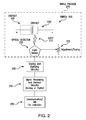
- Figure 2 shows the light emitted from the arc formed between the contact of Figure 1B and an opposing contact of a switch, when the contacts separate.
- the light is shown being detected by the optical detector proximate to the contracts.
- the optical detector and associated electronics detect the characteristic optical spectrum of the light emitted by the arc between the portions of the base layer exposed through the worn areas and the opposing contact.
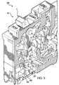
- Figure 3 shows an example of a single package, such as a circuit breaker, with the optical detector located proximate to the switch contacts of Figure 2 , the optical detector configured to detect the light emitted from the arc formed between the contacts when they separate.
- the optical detector and the associated electronics of Figure 2 detect the characteristic optical spectrum of the light emitted by the arc, thereby detecting an amount of wear of the contacts.
- Figure 4A shows an example spectral image of brass, indicating a large peak in the irradiance at a wavelength of 520 nm for brass.
- Figure 4B shows an example spectral image of zinc, indicating there is no peak in the irradiance at 520 nm for zinc.
- Figure lea shows an electrical contact 100 having a base layer composed of a first material, such as brass, and a contacting layer 120 composed of a second material, such as zinc.
- the contacting layer 120 may be configured to electrically contact an opposing contact 100' in a switch 205 shown in Figure 2 .
- an arc 210 occurs, as shown in Figure 1B .
- the presently exposed surface of the contact 100 is locally heated, causing evaporation of some of the material of the exposed surface, which is ionized forming a plasma between the separating contacts 100 and 100'.
- Ions of the evaporated material composing the arc 210 emit light 212 shown in Figure 1B , the light 212 having the characteristic optical spectrum of the material of the exposed surface of the contact 100.
- the characteristic optical spectrum of the light emitted from the arc 210 may be detected by an optical detector 220 shown in Figure 1 B proximate to the contacts and analyzed by connected electronics 230, 240, and 250 shown in Figure 2 .
- the plasma of the arc 210 is composed primarily of second material, (e.g., zinc) ions that emit the characteristic optical spectrum of the second material, (e.g., zinc).
- the characteristic optical spectrum of the second material, (e.g., zinc) is detected and recognized by the optical detector 220 and connected electronics 230, 240, and 250.
- the second material of the contacting layer 120 is eroded by arc erosion, causing the formation of worn areas 125 in the second material coating, which expose the underlying first material of the base layer 110, as shown in Figure 1B .
- the contacts wear there may be a transition period during which both the first material of the base layer 110 and the second material of the contacting layer 120 are eroding and may contribute to the arc 210.
- both materials are contributing to the arc, the light 212 will be emitted from both materials.
- the appearance of the optical spectrum of the first material of the base layer 110 may be gradual as the contacting layer 120 is worn away.
- the first material of the base layer 110 and/or the second material of the contacting layer 120 may be composed of multiple materials that have mutually distinctive optical spectra, so that there may be a gradual change in the composition of the material being eroded by arc erosion. Correspondingly, there is a gradual change in the optical spectrum of the light emitted by the arc as the contacting layer 120 is worn away.
- Figure 1B shows the electrical contact 100 of Figure 1A , wherein the contacting layer 120 has become worn in areas 125 as a result of arc erosion, so that the base layer 110 may have portions exposed through the worn areas 125 of the contacting layer 120.
- the presently exposed surface of the base layer 110 of the first material, such as brass, in the worn areas 125, is locally heated, causing evaporation of some of the first material (e.g., brass), which is ionized forming the plasma between the separating contacts 100 and 100'.
- Figure 1B shows the optical detector located proximate to the contact 100.
- the characteristic optical spectrum of first material e.g., brass
- the characteristic optical spectrum of first material is detected by the optical detector 220 in the single package, i.e. packaging, 200 of the switch 205 and analyzed by the connected electronics 230, 240, and 250 shown in Figure 2 , indicating the worn condition of the contacts.
- the optical detector 220 and connected electronics may discriminate between the spectra for the first and second materials.
- the optical detector 220 and connected electronics may detect an increase in the spectrum intensity emitted from the first material of the base layer 110, as an indication of contact wear In other embodiments of the invention, the optical detector 220 and connected electronics may detect a decrease in the spectrum intensity emitted from the second material of the contacting layer 120, as an indication of contact wear.
- Figure 2 shows the light 212 emitted from the arc 210 formed between the contact 100 of Figure 1B and the opposing contact 100' of the switch 205, when the contacts 100 and 100' separate.
- the light 200 is shown being detected by the optical detector 220 in the single package 200, for example a circuit breaker, which also contains the switch 205.
- the optical detector 220 and associated electronics 230, 240, and 250 detect the characteristic optical spectrum of the light 212 emitted by the arc 210 between the portions of the base layer 110 exposed through the worn areas 125 and the opposing contact 100'.
- the optical detector 220 may be located proximate to the contacts 100 and 100' on the inside of the single package 200 and the associated electronics 230, 240, and 250 may be connected to the optical detector 220 and located on the outside or remotely of the single package 200.
- the associated electronics may include scaling and digitizing circuitry 230, signal processing and decision circuitry (analog or digital) 240, and communication and human-machine interface (HMI) components for indication 250.
- scaling and digitizing circuitry 230 signal processing and decision circuitry (analog or digital) 240
- communication and human-machine interface (HMI) components for indication 250.
- the optical detector 220 may be a cadmium sulfide photocell that is tuned to detect the light 212 having the characteristic optical spectrum of first material (e.g., brass) of the base layer 110. Adjustment and tuning circuitry 225 may be connected to the optical detector 220 to fine-tune the sensitivity of the light sensor/optical detector 220. For example, a cadmium sulfide optical detector 220 may be tuned to detect the 520 nm irradiance peak of brass in the base layer 110.
- first material e.g., brass
- the first material in the base layer 110 may be brass and the second material in the contacting layer 120 may be zinc.
- the first material in the base layer 110 may be copper, nickel, or aluminum and the second material in the contacting layer 120 may be silver, tin, gold, or tungsten carbide.
- the electrical contact 100 may be a component of any switch including but not limited to a contactor, a circuit breaker, or a relay.
- Figure 3 shows a circuit breaker as an example of the single package 200, with the optical detector 220 located proximate to the switch contacts 100 and 100' of Figure 2 .
- the optical detector 220 is configured to detect the light 212 emitted from the arc 210 formed between the contacts 100 and 100' when they separate.
- the associated electronics of Figure 2 may be connected to the optical detector 220 and located outside the circuit breaker.
- the optical detector 220 detects the characteristic optical spectrum of the light 212 emitted by the arc 210, thereby detecting an amount of wear of the contacts 100 and 100' of the circuit breaker.
- the example circuit breaker is shown in the ON state 40 with the operating handle 4 in an ON position.
- the figure shows the operating handle 4 pivotally mounted on a pivot 10 to the inside of the case 3.
- the operating handle 4 is operatively coupled to a contact operating mechanism 20 in the case 3, to open the contacts 100 and 100' when the user moves the operating handle 4 toward the ON position.
- the figure shows a cam 19 of the operating handle 4 being operatively coupled to a current-responsive tripping mechanism 22 in the case 3, to open the contacts 100 and 100' in response to a current-responsive tripping mechanism 22 having detected an over-current in the circuit breaker.
- the optical detector 220 is positioned in the case 3, proximate to the contacts 100 and 100', to detect the light 212 emitted from the arc 210 formed between the contacts 100 and 100', when they are separated either by manual actuation of the operating handle or in response to the current-responsive tripping mechanism.
- Figure 4A shows an example spectral image of brass and Figure 4B shows an example spectral image of zinc. Comparing the spectra of these two materials shows a large peak in the irradiance at a wavelength of 520 nm for brass, which is not present in the irradiance for zinc.
- brass as the base layer 110 and zinc as the contacting layer 120 may be used to indicate the wear of the contacts 100 and 100'. If the contact 100 were coated with zinc, the 520 nm peak in irradiance would only appear after the zinc wore through.
- the invention enables simpler maintenance scheduling, provides early detection of excessive contact wear, promotes extended life of electrical contacts, and eliminates the need to disassemble complex equipment to determine the contact status of component switches.
Landscapes
- Physics & Mathematics (AREA)
- General Physics & Mathematics (AREA)
- Chemical & Material Sciences (AREA)
- Engineering & Computer Science (AREA)
- Composite Materials (AREA)
- Materials Engineering (AREA)
- Photometry And Measurement Of Optical Pulse Characteristics (AREA)
- Arc-Extinguishing Devices That Are Switches (AREA)
Abstract
Description
- The invention disclosed relates wear detection in electrical contacts.
- The switching of electrical currents produces arcing between switch contacts, having the potential to cause considerable damage to the contacts. Metal atoms are eroded and ionized from the contact, resulting in arc erosion. Arc erosion on the contacts of a switch impair good contact joint integrity when the switch is fully closed.
- Contact wear detection is needed to indicate whether switch contacts need replacement. Often, the contacts are either replaced too early or too late in the life cycle, merely on an external schedule or after a set number of operations. Earlier attempts to detect contact wear focused a source of ultraviolet light on a fluorescent trace material previously applied to an electrical contact. The amount of optical fluorescence detected from the UV-illuminated trace material, was related to the amount of wear of the contacts.
- In accordance with an example embodiment of the invention, a contact wear detector in a switch includes an electrical contact having a base layer composed of a first material and a contacting layer composed of a second material. Either one or both of the switch contacts may have a base layer of the first material that is coated with a contacting layer of the second material.
- Each time the contacts open, an arc occurs, wherein the presently exposed surface of the contact is locally heated, causing evaporation of some of the material of the exposed surface, which is ionized forming a plasma between the separating contacts.
- Ions of the evaporated material composing the arc, emit light having the characteristic optical spectrum of the material of the exposed surface.
- The characteristic optical spectrum of the light emitted from the arc, is detected and analyzed by an optical detector in the switch and connected electronics.
- For new switch contacts, only the second material coating is presently exposed and the arc plasma is composed primarily of second material ions that emit the characteristic optical spectrum of second material, which is detected and recognized by the optical detector and connected electronics.
- As time goes on, the second material coating is eroded, causing the formation of worn areas in the second material coating, which expose the underlying first material.
- When the contacts open and an arc occurs, the presently exposed surface of the first material in the worn areas, is locally heated, causing evaporation of some of the first material, which is ionized forming the plasma between the separating contacts.
- The ions of the evaporated first material composing the arc, emit light having the characteristic optical spectrum of first material.
- The characteristic optical spectrum of first material, in the light emitted from the arc, is detected and analyzed by the optical detector in the switch and connected electronics, indicating the worn condition of the contacts.
- In example embodiments, the first material in the base layer may be brass and the second material in the contacting layer may be zinc. In other example embodiments, the first material may be brass, copper, nickel, or aluminum and the second material may be silver, tin, gold, or tungsten carbide. The electrical contact may be a component of a contactor, a circuit breaker, or a relay, as well as a switch.
- The invention enables simpler maintenance scheduling, provides early detection of excessive contact wear, promotes extended life of electrical contacts, and eliminates the need to disassemble complex equipment to determine the contact status of component switches.
- Example embodiments of the invention are depicted in the accompanying drawings that are briefly described as follows:
-
Figure 1A shows an electrical contact having a base layer composed of a first material and a contacting layer composed of a second material, the contacting layer being configured to electrically contact an opposing contact in a switch. -
Figure 1B shows the electrical contact ofFigure 1A , wherein the contacting layer has become worn in areas as a result of arc erosion, the base having portions exposed through the worn areas of the contacting layer. The figure further shows the first material of the base layer forming an arc between the portions of the base layer exposed through the worn areas and the opposing contact when the contacts separate. The figure further shows the arc thus formed emitting light having a gradually increasing component from the first material, which is detected by an optical detector proximate to the contacts. -
Figure 2 shows the light emitted from the arc formed between the contact ofFigure 1B and an opposing contact of a switch, when the contacts separate. The light is shown being detected by the optical detector proximate to the contracts. The optical detector and associated electronics detect the characteristic optical spectrum of the light emitted by the arc between the portions of the base layer exposed through the worn areas and the opposing contact. -
Figure 3 shows an example of a single package, such as a circuit breaker, with the optical detector located proximate to the switch contacts ofFigure 2 , the optical detector configured to detect the light emitted from the arc formed between the contacts when they separate. The optical detector and the associated electronics ofFigure 2 , detect the characteristic optical spectrum of the light emitted by the arc, thereby detecting an amount of wear of the contacts. -
Figure 4A shows an example spectral image of brass, indicating a large peak in the irradiance at a wavelength of 520 nm for brass. -
Figure 4B shows an example spectral image of zinc, indicating there is no peak in the irradiance at 520 nm for zinc. - Figure lea shows an
electrical contact 100 having a base layer composed of a first material, such as brass, and a contactinglayer 120 composed of a second material, such as zinc. The contactinglayer 120 may be configured to electrically contact an opposing contact 100' in aswitch 205 shown inFigure 2 . - Each time the
contacts 100 and 100' open, anarc 210 occurs, as shown inFigure 1B . The presently exposed surface of thecontact 100 is locally heated, causing evaporation of some of the material of the exposed surface, which is ionized forming a plasma between theseparating contacts 100 and 100'. Ions of the evaporated material composing thearc 210,emit light 212 shown inFigure 1B , thelight 212 having the characteristic optical spectrum of the material of the exposed surface of thecontact 100. The characteristic optical spectrum of the light emitted from thearc 210, may be detected by anoptical detector 220 shown inFigure 1 B proximate to the contacts and analyzed by connectedelectronics Figure 2 . - For
new switch contacts 100 and 100', only the second material, such as zinc, in the contactinglayer 120, is presently exposed. The plasma of thearc 210 is composed primarily of second material, (e.g., zinc) ions that emit the characteristic optical spectrum of the second material, (e.g., zinc). The characteristic optical spectrum of the second material, (e.g., zinc). is detected and recognized by theoptical detector 220 and connectedelectronics - As time goes on, the second material of the contacting
layer 120 is eroded by arc erosion, causing the formation ofworn areas 125 in the second material coating, which expose the underlying first material of thebase layer 110, as shown inFigure 1B . As the contacts wear, there may be a transition period during which both the first material of thebase layer 110 and the second material of the contactinglayer 120 are eroding and may contribute to thearc 210. When both materials are contributing to the arc, thelight 212 will be emitted from both materials. The appearance of the optical spectrum of the first material of thebase layer 110 may be gradual as the contactinglayer 120 is worn away. - In alternate embodiments, the first material of the
base layer 110 and/or the second material of the contactinglayer 120 may be composed of multiple materials that have mutually distinctive optical spectra, so that there may be a gradual change in the composition of the material being eroded by arc erosion. Correspondingly, there is a gradual change in the optical spectrum of the light emitted by the arc as the contactinglayer 120 is worn away. -
Figure 1B shows theelectrical contact 100 ofFigure 1A , wherein the contactinglayer 120 has become worn inareas 125 as a result of arc erosion, so that thebase layer 110 may have portions exposed through theworn areas 125 of thecontacting layer 120. - When the
contacts 100 and 100' open and thearc 210 occurs, the presently exposed surface of thebase layer 110 of the first material, such as brass, in theworn areas 125, is locally heated, causing evaporation of some of the first material (e.g., brass), which is ionized forming the plasma between theseparating contacts 100 and 100'. The ions of the evaporated first material (e.g., brass) composing thearc 210, emitlight 212 having the characteristic optical spectrum of first material (e.g., brass). -
Figure 1B shows the optical detector located proximate to thecontact 100. The characteristic optical spectrum of first material (e.g., brass), in thelight 212 emitted from thearc 210, is detected by theoptical detector 220 in the single package, i.e. packaging, 200 of theswitch 205 and analyzed by the connectedelectronics Figure 2 , indicating the worn condition of the contacts. - As discussed above, as the contacts wear, there may be a transition period during which both the first material of the
base layer 110 and the second material of the contactinglayer 120 may be involved in thearc 210, and thelight 212 will be emitted from both materials. Theoptical detector 220 and connected electronics may discriminate between the spectra for the first and second materials. Theoptical detector 220 and connected electronics may detect an increase in the spectrum intensity emitted from the first material of thebase layer 110, as an indication of contact wear In other embodiments of the invention, theoptical detector 220 and connected electronics may detect a decrease in the spectrum intensity emitted from the second material of the contactinglayer 120, as an indication of contact wear. -
Figure 2 shows the light 212 emitted from thearc 210 formed between thecontact 100 ofFigure 1B and the opposing contact 100' of theswitch 205, when thecontacts 100 and 100' separate. The light 200 is shown being detected by theoptical detector 220 in thesingle package 200, for example a circuit breaker, which also contains theswitch 205. Theoptical detector 220 and associatedelectronics arc 210 between the portions of thebase layer 110 exposed through theworn areas 125 and the opposing contact 100'. - The
optical detector 220 may be located proximate to thecontacts 100 and 100' on the inside of thesingle package 200 and the associatedelectronics optical detector 220 and located on the outside or remotely of thesingle package 200. - The associated electronics may include scaling and digitizing
circuitry 230, signal processing and decision circuitry (analog or digital) 240, and communication and human-machine interface (HMI) components forindication 250. - The
optical detector 220 may be a cadmium sulfide photocell that is tuned to detect the light 212 having the characteristic optical spectrum of first material (e.g., brass) of thebase layer 110. Adjustment andtuning circuitry 225 may be connected to theoptical detector 220 to fine-tune the sensitivity of the light sensor/optical detector 220. For example, a cadmium sulfideoptical detector 220 may be tuned to detect the 520 nm irradiance peak of brass in thebase layer 110. - In example embodiments, the first material in the
base layer 110 may be brass and the second material in the contactinglayer 120 may be zinc. In other example embodiments, the first material in thebase layer 110 may be copper, nickel, or aluminum and the second material in the contactinglayer 120 may be silver, tin, gold, or tungsten carbide. Theelectrical contact 100 may be a component of any switch including but not limited to a contactor, a circuit breaker, or a relay. -
Figure 3 shows a circuit breaker as an example of thesingle package 200, with theoptical detector 220 located proximate to theswitch contacts 100 and 100' ofFigure 2 . Theoptical detector 220 is configured to detect the light 212 emitted from thearc 210 formed between thecontacts 100 and 100' when they separate. The associated electronics ofFigure 2 may be connected to theoptical detector 220 and located outside the circuit breaker. Theoptical detector 220 detects the characteristic optical spectrum of the light 212 emitted by thearc 210, thereby detecting an amount of wear of thecontacts 100 and 100' of the circuit breaker. - The example circuit breaker is shown in the
ON state 40 with theoperating handle 4 in an ON position. The figure shows theoperating handle 4 pivotally mounted on apivot 10 to the inside of thecase 3. Theoperating handle 4 is operatively coupled to acontact operating mechanism 20 in thecase 3, to open thecontacts 100 and 100' when the user moves theoperating handle 4 toward the ON position. The figure shows acam 19 of theoperating handle 4 being operatively coupled to a current-responsive trippingmechanism 22 in thecase 3, to open thecontacts 100 and 100' in response to a current-responsive trippingmechanism 22 having detected an over-current in the circuit breaker. Theoptical detector 220 is positioned in thecase 3, proximate to thecontacts 100 and 100', to detect the light 212 emitted from thearc 210 formed between thecontacts 100 and 100', when they are separated either by manual actuation of the operating handle or in response to the current-responsive tripping mechanism. - Two common materials used in making contacts are brass and zinc.
Figure 4A shows an example spectral image of brass andFigure 4B shows an example spectral image of zinc. Comparing the spectra of these two materials shows a large peak in the irradiance at a wavelength of 520 nm for brass, which is not present in the irradiance for zinc. Thus, brass as thebase layer 110 and zinc as the contactinglayer 120 may be used to indicate the wear of thecontacts 100 and 100'. If thecontact 100 were coated with zinc, the 520 nm peak in irradiance would only appear after the zinc wore through. - The invention enables simpler maintenance scheduling, provides early detection of excessive contact wear, promotes extended life of electrical contacts, and eliminates the need to disassemble complex equipment to determine the contact status of component switches.
- Although specific example embodiments of the invention have been disclosed, persons of skill in the art will appreciate that changes may be made to the details described for the specific example embodiments, without departing from the spirit and the scope of the invention.
Claims (9)
- A contact wear detector, comprising:an electrical contact having a base layer composed of a first material and a contacting layer composed of a second material, the contacting layer being configured to electrically contact an opposing contact in a switch, the base layer being capable of having portions exposed through worn areas of the contacting layer, the first material of the base layer being configured to form an arc between the portions of the base layer exposed through the worn areas and the opposing contact when the contacts separate, the arc thus formed emitting light having a characteristic optical spectrum of the first material; andan optical detector proximate to the electrical contact, the optical detector being configured to detect the characteristic optical spectrum of the light emitted by the arc between the portions of the base layer exposed through the worn areas and the opposing contact.
- The contact wear detector, of claim 1, wherein the first material of the base layer is brass and the second material of the contact layer is zinc.
- The contact wear detector, of claim 1, wherein the electrical contact is a component of a switch comprising one of a contactor, a circuit breaker, and a relay.
- The contact wear detector, of claim 1, wherein both the electrical contact and the optical detector are components of a single package.
- The contact wear detector, of claim 1, wherein both the first material of the base layer and the second material of the contacting layer contribute to forming an arc with the opposing contact when the contacts separate, the arc thus formed emitting light having characteristic optical spectra of both the first material and the second material; and
the optical detector proximate to the electrical contact being configured to detect the characteristic optical spectra of both the first material and the second material. - The contact wear detector, of claim 5, wherein contact wear is detected by an increase in spectrum intensity emitted from the first material of the base layer.
- The contact wear detector, of claim 5, wherein contact wear is detected by a decrease in spectrum intensity emitted from the second material of the contacting layer.
- The contact wear detector, of claim 1, wherein the first material of the base layer is composed of multiple materials that have mutually distinctive optical spectra, so that there is a gradual change in composition of the first material being eroded by arc erosion.
- The contact wear detector, of claim 1, wherein the second material of the contacting layer is composed of multiple materials that have mutually distinctive optical spectra, so that there is a gradual change in composition of the second material being eroded by arc erosion.
Applications Claiming Priority (1)
| Application Number | Priority Date | Filing Date | Title |
|---|---|---|---|
| US14/541,786 US9329238B1 (en) | 2014-11-14 | 2014-11-14 | Contact wear detection by spectral analysis shift |
Publications (2)
| Publication Number | Publication Date |
|---|---|
| EP3021338A1 true EP3021338A1 (en) | 2016-05-18 |
| EP3021338B1 EP3021338B1 (en) | 2023-04-05 |
Family
ID=54544956
Family Applications (1)
| Application Number | Title | Priority Date | Filing Date |
|---|---|---|---|
| EP15194437.8A Active EP3021338B1 (en) | 2014-11-14 | 2015-11-13 | Contact wear detection by spectral analysis shift |
Country Status (3)
| Country | Link |
|---|---|
| US (1) | US9329238B1 (en) |
| EP (1) | EP3021338B1 (en) |
| CN (1) | CN105609331B (en) |
Cited By (1)
| Publication number | Priority date | Publication date | Assignee | Title |
|---|---|---|---|---|
| EP4553881A1 (en) * | 2023-11-10 | 2025-05-14 | Safran Electrical & Power | Apparatus comprising an electrical contact provided with a brightness sensor and method for estimating wear |
Families Citing this family (10)
| Publication number | Priority date | Publication date | Assignee | Title |
|---|---|---|---|---|
| US9885659B1 (en) | 2016-10-04 | 2018-02-06 | International Business Machines Corporation | Method to determine connector metal wear via flouresence |
| FR3060758B1 (en) * | 2016-12-16 | 2021-01-08 | Schneider Electric Ind Sas | METHOD AND DEVICE FOR DIAGNOSING THE WEAR OF AN ELECTRIC SWITCHING APPARATUS, AND ELECTRICAL APPARATUS INCLUDING SUCH A DEVICE |
| CN106842009B (en) * | 2017-01-17 | 2017-11-07 | 国网山东省电力公司乳山市供电公司 | A kind of contacts for vacuum-break switches disjunction detection means |
| US11181462B2 (en) | 2018-11-30 | 2021-11-23 | International Business Machines Corporation | Non-destructive method to determine porosity in metallic coatings |
| JP7263530B2 (en) * | 2019-02-18 | 2023-04-24 | エルエス、エレクトリック、カンパニー、リミテッド | Vacuum circuit breaker contact monitoring device and vacuum circuit breaker including the same |
| US10872739B2 (en) | 2019-05-24 | 2020-12-22 | Frank P Stacom | Methods and systems for DC current interrupter based on thermionic arc extinction via anode ion depletion |
| WO2021049733A1 (en) * | 2019-09-10 | 2021-03-18 | 엘에스일렉트릭(주) | Contact monitoring device for vacuum circuit breaker and vacuum circuit breaker having same |
| CN112378865B (en) * | 2020-12-11 | 2024-07-19 | 广东电网有限责任公司 | A contact finger detection system for isolating switch |
| US11874314B2 (en) | 2022-02-09 | 2024-01-16 | Caterpillar Inc. | Electrical contact wear monitoring system |
| CN120043941B (en) * | 2025-02-24 | 2025-11-14 | 福州大学 | Arc erosion mechanism capable of moving back and forth |
Citations (6)
| Publication number | Priority date | Publication date | Assignee | Title |
|---|---|---|---|---|
| JPS51114677A (en) * | 1975-03-31 | 1976-10-08 | Matsushita Electric Works Ltd | Contact device |
| JPS51114678A (en) * | 1975-03-31 | 1976-10-08 | Matsushita Electric Works Ltd | Contacts |
| US6023036A (en) * | 1996-09-10 | 2000-02-08 | Nichols; Bruce W. | Electrical contact wear and temperature indicator |
| US20050040020A1 (en) * | 2003-08-22 | 2005-02-24 | Yukio Kanazawa | Electric contacts, electric contact apparatus and method for detecting abrasion of the electric contacts |
| US20050104598A1 (en) * | 2002-09-11 | 2005-05-19 | Nicola Dominelli | Method and apparatus for detecting wear in components of high voltage electrical equipment |
| EP1895554A1 (en) * | 2006-09-04 | 2008-03-05 | ABB Research Ltd | Electrical contact with signal zone for signaling contact-wear |
Family Cites Families (9)
| Publication number | Priority date | Publication date | Assignee | Title |
|---|---|---|---|---|
| DE3120856A1 (en) * | 1981-05-26 | 1982-12-23 | Leybold-Heraeus GmbH, 5000 Köln | METHOD FOR MONITORING THE MELTING PROCESS IN VACUUM ARC FURNACES |
| SE433546B (en) | 1982-10-25 | 1984-05-28 | Asea Ab | DEVICE CONTROL CONTROL OF AN ELECTRICAL DEVICE DEVICE FOR CONTROL CONVERSION OF AN ELECTRICAL DEVICE |
| US6884998B2 (en) * | 2002-12-13 | 2005-04-26 | Nichols Applied Technology, Llc | Method and apparatus for determining electrical contact wear |
| US7038201B2 (en) | 2002-12-13 | 2006-05-02 | Nichols Applied Technology, Llc | Method and apparatus for determining electrical contact wear |
| DE10345183B4 (en) | 2003-09-29 | 2005-10-13 | Siemens Ag | Device for detecting contact erosion in switching devices |
| DE102004001799B4 (en) * | 2004-01-05 | 2008-12-11 | Pantrac Gmbh | Sensor device for signaling wear conditions on grinding wheels |
| DE102005046925A1 (en) * | 2005-09-30 | 2007-04-19 | Siemens Ag | Switching device for switching at least one current |
| JP5032091B2 (en) * | 2006-10-12 | 2012-09-26 | 株式会社東芝 | Gas insulated switchgear and arc damage detection method for gas insulated switchgear parts |
| CN101469971B (en) * | 2007-12-26 | 2010-11-03 | 上海西屋开关有限公司 | Method and apparatus for detecting contact head abrasive loss of vacuum circuit breaker |
-
2014
- 2014-11-14 US US14/541,786 patent/US9329238B1/en active Active
-
2015
- 2015-11-09 CN CN201510755520.8A patent/CN105609331B/en active Active
- 2015-11-13 EP EP15194437.8A patent/EP3021338B1/en active Active
Patent Citations (6)
| Publication number | Priority date | Publication date | Assignee | Title |
|---|---|---|---|---|
| JPS51114677A (en) * | 1975-03-31 | 1976-10-08 | Matsushita Electric Works Ltd | Contact device |
| JPS51114678A (en) * | 1975-03-31 | 1976-10-08 | Matsushita Electric Works Ltd | Contacts |
| US6023036A (en) * | 1996-09-10 | 2000-02-08 | Nichols; Bruce W. | Electrical contact wear and temperature indicator |
| US20050104598A1 (en) * | 2002-09-11 | 2005-05-19 | Nicola Dominelli | Method and apparatus for detecting wear in components of high voltage electrical equipment |
| US20050040020A1 (en) * | 2003-08-22 | 2005-02-24 | Yukio Kanazawa | Electric contacts, electric contact apparatus and method for detecting abrasion of the electric contacts |
| EP1895554A1 (en) * | 2006-09-04 | 2008-03-05 | ABB Research Ltd | Electrical contact with signal zone for signaling contact-wear |
Cited By (2)
| Publication number | Priority date | Publication date | Assignee | Title |
|---|---|---|---|---|
| EP4553881A1 (en) * | 2023-11-10 | 2025-05-14 | Safran Electrical & Power | Apparatus comprising an electrical contact provided with a brightness sensor and method for estimating wear |
| FR3155357A1 (en) * | 2023-11-10 | 2025-05-16 | Safran Electrical & Power | Device comprising an electrical contact equipped with a brightness sensor and method for estimating wear |
Also Published As
| Publication number | Publication date |
|---|---|
| EP3021338B1 (en) | 2023-04-05 |
| CN105609331A (en) | 2016-05-25 |
| US9329238B1 (en) | 2016-05-03 |
| US20160139206A1 (en) | 2016-05-19 |
| CN105609331B (en) | 2020-05-19 |
Similar Documents
| Publication | Publication Date | Title |
|---|---|---|
| US9329238B1 (en) | Contact wear detection by spectral analysis shift | |
| FR2802721A1 (en) | Equipment for detecting arcs and communicating subsequent switch operations, comprises current detector, broad band noise detection circuits, microcontroller and switching data communication channel | |
| CA2783683C (en) | Electronic miniature circuit breaker with trip indication using the breaker tripping function as the feedback mechanism | |
| CN108226769B (en) | System and method for monitoring contact life of a circuit interrupter | |
| JP4334299B2 (en) | Electrical contact, electrical contact wear detection device and wear detection method thereof | |
| FR2802722A1 (en) | Equipment for identifying presence of an arc in an electrical circuit, comprises rate of change of current sensor, circuit for detecting wide band noise and microcontroller to determine if arc exists | |
| US10320176B2 (en) | Method for distinguishing an arc from a luminous gas containing at least metal vapor | |
| US20190074153A1 (en) | Circuit Interrupter With Status Indication | |
| JP7327853B2 (en) | Plasma therapy on the surface of power contact electrodes | |
| US5548461A (en) | Arc suppressor | |
| Miller | On sputtering in vacuum arcs | |
| JP2006515419A (en) | Method and apparatus for detecting wear in components of high voltage electrical equipment | |
| JP4097432B2 (en) | Accidental arc identification method and apparatus | |
| Takeuchi et al. | The spatial distributions of spectral intensity and temperature in the cross section of an arc column between separating Pd contacts | |
| EP0047696B1 (en) | Miniature circuit breaker with arcing-contacts | |
| US2627564A (en) | Electric circuit breaker | |
| Mützel et al. | Contact material solutions for LED lamp application | |
| US8243409B2 (en) | Protective device and method for its operation | |
| EP3718126B1 (en) | Modular electrical switching device | |
| Akbi | Effect of heat surface treatment on photoelectric work function of silver-metal alloys | |
| Qu et al. | Application of laser arc imaging technology to observe arc behavior and contact motion | |
| CN105990059A (en) | Momentary contact switch and method of activating the momentary contact switch | |
| WO2020240097A1 (en) | Electric line (l) protection device for detecting a leakage fault, a short-circuit, fault, an overcurrent fault and an arc fault | |
| US2331162A (en) | Electrical switch | |
| TWI691095B (en) | Dual-band optical detector and preparation method thereof |
Legal Events
| Date | Code | Title | Description |
|---|---|---|---|
| PUAI | Public reference made under article 153(3) epc to a published international application that has entered the european phase |
Free format text: ORIGINAL CODE: 0009012 |
|
| AK | Designated contracting states |
Kind code of ref document: A1 Designated state(s): AL AT BE BG CH CY CZ DE DK EE ES FI FR GB GR HR HU IE IS IT LI LT LU LV MC MK MT NL NO PL PT RO RS SE SI SK SM TR |
|
| AX | Request for extension of the european patent |
Extension state: BA ME |
|
| 17P | Request for examination filed |
Effective date: 20161024 |
|
| RBV | Designated contracting states (corrected) |
Designated state(s): AL AT BE BG CH CY CZ DE DK EE ES FI FR GB GR HR HU IE IS IT LI LT LU LV MC MK MT NL NO PL PT RO RS SE SI SK SM TR |
|
| STAA | Information on the status of an ep patent application or granted ep patent |
Free format text: STATUS: EXAMINATION IS IN PROGRESS |
|
| 17Q | First examination report despatched |
Effective date: 20180604 |
|
| GRAP | Despatch of communication of intention to grant a patent |
Free format text: ORIGINAL CODE: EPIDOSNIGR1 |
|
| STAA | Information on the status of an ep patent application or granted ep patent |
Free format text: STATUS: GRANT OF PATENT IS INTENDED |
|
| INTG | Intention to grant announced |
Effective date: 20221020 |
|
| GRAS | Grant fee paid |
Free format text: ORIGINAL CODE: EPIDOSNIGR3 |
|
| GRAA | (expected) grant |
Free format text: ORIGINAL CODE: 0009210 |
|
| STAA | Information on the status of an ep patent application or granted ep patent |
Free format text: STATUS: THE PATENT HAS BEEN GRANTED |
|
| AK | Designated contracting states |
Kind code of ref document: B1 Designated state(s): AL AT BE BG CH CY CZ DE DK EE ES FI FR GB GR HR HU IE IS IT LI LT LU LV MC MK MT NL NO PL PT RO RS SE SI SK SM TR |
|
| REG | Reference to a national code |
Ref country code: GB Ref legal event code: FG4D |
|
| REG | Reference to a national code |
Ref country code: CH Ref legal event code: EP |
|
| REG | Reference to a national code |
Ref country code: AT Ref legal event code: REF Ref document number: 1558884 Country of ref document: AT Kind code of ref document: T Effective date: 20230415 |
|
| REG | Reference to a national code |
Ref country code: DE Ref legal event code: R096 Ref document number: 602015083036 Country of ref document: DE |
|
| REG | Reference to a national code |
Ref country code: IE Ref legal event code: FG4D |
|
| REG | Reference to a national code |
Ref country code: LT Ref legal event code: MG9D |
|
| REG | Reference to a national code |
Ref country code: NL Ref legal event code: MP Effective date: 20230405 |
|
| REG | Reference to a national code |
Ref country code: AT Ref legal event code: MK05 Ref document number: 1558884 Country of ref document: AT Kind code of ref document: T Effective date: 20230405 |
|
| PG25 | Lapsed in a contracting state [announced via postgrant information from national office to epo] |
Ref country code: NL Free format text: LAPSE BECAUSE OF FAILURE TO SUBMIT A TRANSLATION OF THE DESCRIPTION OR TO PAY THE FEE WITHIN THE PRESCRIBED TIME-LIMIT Effective date: 20230405 |
|
| PG25 | Lapsed in a contracting state [announced via postgrant information from national office to epo] |
Ref country code: SE Free format text: LAPSE BECAUSE OF FAILURE TO SUBMIT A TRANSLATION OF THE DESCRIPTION OR TO PAY THE FEE WITHIN THE PRESCRIBED TIME-LIMIT Effective date: 20230405 Ref country code: PT Free format text: LAPSE BECAUSE OF FAILURE TO SUBMIT A TRANSLATION OF THE DESCRIPTION OR TO PAY THE FEE WITHIN THE PRESCRIBED TIME-LIMIT Effective date: 20230807 Ref country code: NO Free format text: LAPSE BECAUSE OF FAILURE TO SUBMIT A TRANSLATION OF THE DESCRIPTION OR TO PAY THE FEE WITHIN THE PRESCRIBED TIME-LIMIT Effective date: 20230705 Ref country code: ES Free format text: LAPSE BECAUSE OF FAILURE TO SUBMIT A TRANSLATION OF THE DESCRIPTION OR TO PAY THE FEE WITHIN THE PRESCRIBED TIME-LIMIT Effective date: 20230405 Ref country code: AT Free format text: LAPSE BECAUSE OF FAILURE TO SUBMIT A TRANSLATION OF THE DESCRIPTION OR TO PAY THE FEE WITHIN THE PRESCRIBED TIME-LIMIT Effective date: 20230405 |
|
| PG25 | Lapsed in a contracting state [announced via postgrant information from national office to epo] |
Ref country code: RS Free format text: LAPSE BECAUSE OF FAILURE TO SUBMIT A TRANSLATION OF THE DESCRIPTION OR TO PAY THE FEE WITHIN THE PRESCRIBED TIME-LIMIT Effective date: 20230405 Ref country code: PL Free format text: LAPSE BECAUSE OF FAILURE TO SUBMIT A TRANSLATION OF THE DESCRIPTION OR TO PAY THE FEE WITHIN THE PRESCRIBED TIME-LIMIT Effective date: 20230405 Ref country code: LV Free format text: LAPSE BECAUSE OF FAILURE TO SUBMIT A TRANSLATION OF THE DESCRIPTION OR TO PAY THE FEE WITHIN THE PRESCRIBED TIME-LIMIT Effective date: 20230405 Ref country code: LT Free format text: LAPSE BECAUSE OF FAILURE TO SUBMIT A TRANSLATION OF THE DESCRIPTION OR TO PAY THE FEE WITHIN THE PRESCRIBED TIME-LIMIT Effective date: 20230405 Ref country code: IS Free format text: LAPSE BECAUSE OF FAILURE TO SUBMIT A TRANSLATION OF THE DESCRIPTION OR TO PAY THE FEE WITHIN THE PRESCRIBED TIME-LIMIT Effective date: 20230805 Ref country code: HR Free format text: LAPSE BECAUSE OF FAILURE TO SUBMIT A TRANSLATION OF THE DESCRIPTION OR TO PAY THE FEE WITHIN THE PRESCRIBED TIME-LIMIT Effective date: 20230405 Ref country code: GR Free format text: LAPSE BECAUSE OF FAILURE TO SUBMIT A TRANSLATION OF THE DESCRIPTION OR TO PAY THE FEE WITHIN THE PRESCRIBED TIME-LIMIT Effective date: 20230706 Ref country code: AL Free format text: LAPSE BECAUSE OF FAILURE TO SUBMIT A TRANSLATION OF THE DESCRIPTION OR TO PAY THE FEE WITHIN THE PRESCRIBED TIME-LIMIT Effective date: 20230405 |
|
| PG25 | Lapsed in a contracting state [announced via postgrant information from national office to epo] |
Ref country code: FI Free format text: LAPSE BECAUSE OF FAILURE TO SUBMIT A TRANSLATION OF THE DESCRIPTION OR TO PAY THE FEE WITHIN THE PRESCRIBED TIME-LIMIT Effective date: 20230405 |
|
| REG | Reference to a national code |
Ref country code: DE Ref legal event code: R097 Ref document number: 602015083036 Country of ref document: DE |
|
| PG25 | Lapsed in a contracting state [announced via postgrant information from national office to epo] |
Ref country code: SK Free format text: LAPSE BECAUSE OF FAILURE TO SUBMIT A TRANSLATION OF THE DESCRIPTION OR TO PAY THE FEE WITHIN THE PRESCRIBED TIME-LIMIT Effective date: 20230405 |
|
| PG25 | Lapsed in a contracting state [announced via postgrant information from national office to epo] |
Ref country code: SM Free format text: LAPSE BECAUSE OF FAILURE TO SUBMIT A TRANSLATION OF THE DESCRIPTION OR TO PAY THE FEE WITHIN THE PRESCRIBED TIME-LIMIT Effective date: 20230405 Ref country code: SK Free format text: LAPSE BECAUSE OF FAILURE TO SUBMIT A TRANSLATION OF THE DESCRIPTION OR TO PAY THE FEE WITHIN THE PRESCRIBED TIME-LIMIT Effective date: 20230405 Ref country code: RO Free format text: LAPSE BECAUSE OF FAILURE TO SUBMIT A TRANSLATION OF THE DESCRIPTION OR TO PAY THE FEE WITHIN THE PRESCRIBED TIME-LIMIT Effective date: 20230405 Ref country code: EE Free format text: LAPSE BECAUSE OF FAILURE TO SUBMIT A TRANSLATION OF THE DESCRIPTION OR TO PAY THE FEE WITHIN THE PRESCRIBED TIME-LIMIT Effective date: 20230405 Ref country code: DK Free format text: LAPSE BECAUSE OF FAILURE TO SUBMIT A TRANSLATION OF THE DESCRIPTION OR TO PAY THE FEE WITHIN THE PRESCRIBED TIME-LIMIT Effective date: 20230405 Ref country code: CZ Free format text: LAPSE BECAUSE OF FAILURE TO SUBMIT A TRANSLATION OF THE DESCRIPTION OR TO PAY THE FEE WITHIN THE PRESCRIBED TIME-LIMIT Effective date: 20230405 |
|
| PLBE | No opposition filed within time limit |
Free format text: ORIGINAL CODE: 0009261 |
|
| STAA | Information on the status of an ep patent application or granted ep patent |
Free format text: STATUS: NO OPPOSITION FILED WITHIN TIME LIMIT |
|
| 26N | No opposition filed |
Effective date: 20240108 |
|
| PG25 | Lapsed in a contracting state [announced via postgrant information from national office to epo] |
Ref country code: SI Free format text: LAPSE BECAUSE OF FAILURE TO SUBMIT A TRANSLATION OF THE DESCRIPTION OR TO PAY THE FEE WITHIN THE PRESCRIBED TIME-LIMIT Effective date: 20230405 |
|
| PG25 | Lapsed in a contracting state [announced via postgrant information from national office to epo] |
Ref country code: SI Free format text: LAPSE BECAUSE OF FAILURE TO SUBMIT A TRANSLATION OF THE DESCRIPTION OR TO PAY THE FEE WITHIN THE PRESCRIBED TIME-LIMIT Effective date: 20230405 Ref country code: IT Free format text: LAPSE BECAUSE OF FAILURE TO SUBMIT A TRANSLATION OF THE DESCRIPTION OR TO PAY THE FEE WITHIN THE PRESCRIBED TIME-LIMIT Effective date: 20230405 |
|
| REG | Reference to a national code |
Ref country code: CH Ref legal event code: PL |
|
| PG25 | Lapsed in a contracting state [announced via postgrant information from national office to epo] |
Ref country code: MC Free format text: LAPSE BECAUSE OF FAILURE TO SUBMIT A TRANSLATION OF THE DESCRIPTION OR TO PAY THE FEE WITHIN THE PRESCRIBED TIME-LIMIT Effective date: 20230405 |
|
| PG25 | Lapsed in a contracting state [announced via postgrant information from national office to epo] |
Ref country code: LU Free format text: LAPSE BECAUSE OF NON-PAYMENT OF DUE FEES Effective date: 20231113 |
|
| PG25 | Lapsed in a contracting state [announced via postgrant information from national office to epo] |
Ref country code: CH Free format text: LAPSE BECAUSE OF NON-PAYMENT OF DUE FEES Effective date: 20231130 |
|
| PG25 | Lapsed in a contracting state [announced via postgrant information from national office to epo] |
Ref country code: MC Free format text: LAPSE BECAUSE OF FAILURE TO SUBMIT A TRANSLATION OF THE DESCRIPTION OR TO PAY THE FEE WITHIN THE PRESCRIBED TIME-LIMIT Effective date: 20230405 Ref country code: LU Free format text: LAPSE BECAUSE OF NON-PAYMENT OF DUE FEES Effective date: 20231113 Ref country code: CH Free format text: LAPSE BECAUSE OF NON-PAYMENT OF DUE FEES Effective date: 20231130 |
|
| REG | Reference to a national code |
Ref country code: BE Ref legal event code: MM Effective date: 20231130 |
|
| REG | Reference to a national code |
Ref country code: IE Ref legal event code: MM4A |
|
| PG25 | Lapsed in a contracting state [announced via postgrant information from national office to epo] |
Ref country code: IE Free format text: LAPSE BECAUSE OF NON-PAYMENT OF DUE FEES Effective date: 20231113 |
|
| PG25 | Lapsed in a contracting state [announced via postgrant information from national office to epo] |
Ref country code: BE Free format text: LAPSE BECAUSE OF NON-PAYMENT OF DUE FEES Effective date: 20231130 |
|
| PG25 | Lapsed in a contracting state [announced via postgrant information from national office to epo] |
Ref country code: IE Free format text: LAPSE BECAUSE OF NON-PAYMENT OF DUE FEES Effective date: 20231113 Ref country code: BE Free format text: LAPSE BECAUSE OF NON-PAYMENT OF DUE FEES Effective date: 20231130 |
|
| PG25 | Lapsed in a contracting state [announced via postgrant information from national office to epo] |
Ref country code: BG Free format text: LAPSE BECAUSE OF FAILURE TO SUBMIT A TRANSLATION OF THE DESCRIPTION OR TO PAY THE FEE WITHIN THE PRESCRIBED TIME-LIMIT Effective date: 20230405 |
|
| PG25 | Lapsed in a contracting state [announced via postgrant information from national office to epo] |
Ref country code: BG Free format text: LAPSE BECAUSE OF FAILURE TO SUBMIT A TRANSLATION OF THE DESCRIPTION OR TO PAY THE FEE WITHIN THE PRESCRIBED TIME-LIMIT Effective date: 20230405 |
|
| PG25 | Lapsed in a contracting state [announced via postgrant information from national office to epo] |
Ref country code: CY Free format text: LAPSE BECAUSE OF FAILURE TO SUBMIT A TRANSLATION OF THE DESCRIPTION OR TO PAY THE FEE WITHIN THE PRESCRIBED TIME-LIMIT; INVALID AB INITIO Effective date: 20151113 |
|
| PG25 | Lapsed in a contracting state [announced via postgrant information from national office to epo] |
Ref country code: HU Free format text: LAPSE BECAUSE OF FAILURE TO SUBMIT A TRANSLATION OF THE DESCRIPTION OR TO PAY THE FEE WITHIN THE PRESCRIBED TIME-LIMIT; INVALID AB INITIO Effective date: 20151113 |
|
| PG25 | Lapsed in a contracting state [announced via postgrant information from national office to epo] |
Ref country code: TR Free format text: LAPSE BECAUSE OF FAILURE TO SUBMIT A TRANSLATION OF THE DESCRIPTION OR TO PAY THE FEE WITHIN THE PRESCRIBED TIME-LIMIT Effective date: 20230405 |
|
| PGFP | Annual fee paid to national office [announced via postgrant information from national office to epo] |
Ref country code: DE Payment date: 20251126 Year of fee payment: 11 |
|
| PGFP | Annual fee paid to national office [announced via postgrant information from national office to epo] |
Ref country code: GB Payment date: 20251125 Year of fee payment: 11 |
|
| PGFP | Annual fee paid to national office [announced via postgrant information from national office to epo] |
Ref country code: FR Payment date: 20251124 Year of fee payment: 11 |