EP3016166A1 - Organic light-emitting display apparatus - Google Patents
Organic light-emitting display apparatus Download PDFInfo
- Publication number
- EP3016166A1 EP3016166A1 EP15191679.8A EP15191679A EP3016166A1 EP 3016166 A1 EP3016166 A1 EP 3016166A1 EP 15191679 A EP15191679 A EP 15191679A EP 3016166 A1 EP3016166 A1 EP 3016166A1
- Authority
- EP
- European Patent Office
- Prior art keywords
- substrate
- organic light
- encapsulating layer
- display apparatus
- electrodes
- Prior art date
- Legal status (The legal status is an assumption and is not a legal conclusion. Google has not performed a legal analysis and makes no representation as to the accuracy of the status listed.)
- Granted
Links
Images




Classifications
-
- H—ELECTRICITY
- H10—SEMICONDUCTOR DEVICES; ELECTRIC SOLID-STATE DEVICES NOT OTHERWISE PROVIDED FOR
- H10K—ORGANIC ELECTRIC SOLID-STATE DEVICES
- H10K59/00—Integrated devices, or assemblies of multiple devices, comprising at least one organic light-emitting element covered by group H10K50/00
- H10K59/30—Devices specially adapted for multicolour light emission
- H10K59/35—Devices specially adapted for multicolour light emission comprising red-green-blue [RGB] subpixels
-
- H—ELECTRICITY
- H10—SEMICONDUCTOR DEVICES; ELECTRIC SOLID-STATE DEVICES NOT OTHERWISE PROVIDED FOR
- H10K—ORGANIC ELECTRIC SOLID-STATE DEVICES
- H10K59/00—Integrated devices, or assemblies of multiple devices, comprising at least one organic light-emitting element covered by group H10K50/00
- H10K59/80—Constructional details
- H10K59/87—Passivation; Containers; Encapsulations
- H10K59/873—Encapsulations
-
- H—ELECTRICITY
- H10—SEMICONDUCTOR DEVICES; ELECTRIC SOLID-STATE DEVICES NOT OTHERWISE PROVIDED FOR
- H10K—ORGANIC ELECTRIC SOLID-STATE DEVICES
- H10K50/00—Organic light-emitting devices
- H10K50/10—OLEDs or polymer light-emitting diodes [PLED]
- H10K50/11—OLEDs or polymer light-emitting diodes [PLED] characterised by the electroluminescent [EL] layers
-
- H—ELECTRICITY
- H10—SEMICONDUCTOR DEVICES; ELECTRIC SOLID-STATE DEVICES NOT OTHERWISE PROVIDED FOR
- H10K—ORGANIC ELECTRIC SOLID-STATE DEVICES
- H10K50/00—Organic light-emitting devices
- H10K50/80—Constructional details
- H10K50/805—Electrodes
- H10K50/81—Anodes
-
- H—ELECTRICITY
- H10—SEMICONDUCTOR DEVICES; ELECTRIC SOLID-STATE DEVICES NOT OTHERWISE PROVIDED FOR
- H10K—ORGANIC ELECTRIC SOLID-STATE DEVICES
- H10K50/00—Organic light-emitting devices
- H10K50/80—Constructional details
- H10K50/805—Electrodes
- H10K50/82—Cathodes
-
- H—ELECTRICITY
- H10—SEMICONDUCTOR DEVICES; ELECTRIC SOLID-STATE DEVICES NOT OTHERWISE PROVIDED FOR
- H10K—ORGANIC ELECTRIC SOLID-STATE DEVICES
- H10K50/00—Organic light-emitting devices
- H10K50/80—Constructional details
- H10K50/84—Passivation; Containers; Encapsulations
- H10K50/844—Encapsulations
-
- H—ELECTRICITY
- H10—SEMICONDUCTOR DEVICES; ELECTRIC SOLID-STATE DEVICES NOT OTHERWISE PROVIDED FOR
- H10K—ORGANIC ELECTRIC SOLID-STATE DEVICES
- H10K50/00—Organic light-emitting devices
- H10K50/80—Constructional details
- H10K50/84—Passivation; Containers; Encapsulations
- H10K50/844—Encapsulations
- H10K50/8445—Encapsulations multilayered coatings having a repetitive structure, e.g. having multiple organic-inorganic bilayers
-
- H—ELECTRICITY
- H10—SEMICONDUCTOR DEVICES; ELECTRIC SOLID-STATE DEVICES NOT OTHERWISE PROVIDED FOR
- H10K—ORGANIC ELECTRIC SOLID-STATE DEVICES
- H10K50/00—Organic light-emitting devices
- H10K50/80—Constructional details
- H10K50/85—Arrangements for extracting light from the devices
- H10K50/858—Arrangements for extracting light from the devices comprising refractive means, e.g. lenses
-
- H—ELECTRICITY
- H10—SEMICONDUCTOR DEVICES; ELECTRIC SOLID-STATE DEVICES NOT OTHERWISE PROVIDED FOR
- H10K—ORGANIC ELECTRIC SOLID-STATE DEVICES
- H10K59/00—Integrated devices, or assemblies of multiple devices, comprising at least one organic light-emitting element covered by group H10K50/00
- H10K59/80—Constructional details
- H10K59/805—Electrodes
- H10K59/8051—Anodes
-
- H—ELECTRICITY
- H10—SEMICONDUCTOR DEVICES; ELECTRIC SOLID-STATE DEVICES NOT OTHERWISE PROVIDED FOR
- H10K—ORGANIC ELECTRIC SOLID-STATE DEVICES
- H10K59/00—Integrated devices, or assemblies of multiple devices, comprising at least one organic light-emitting element covered by group H10K50/00
- H10K59/80—Constructional details
- H10K59/805—Electrodes
- H10K59/8052—Cathodes
-
- H—ELECTRICITY
- H10—SEMICONDUCTOR DEVICES; ELECTRIC SOLID-STATE DEVICES NOT OTHERWISE PROVIDED FOR
- H10K—ORGANIC ELECTRIC SOLID-STATE DEVICES
- H10K59/00—Integrated devices, or assemblies of multiple devices, comprising at least one organic light-emitting element covered by group H10K50/00
- H10K59/80—Constructional details
- H10K59/87—Passivation; Containers; Encapsulations
- H10K59/873—Encapsulations
- H10K59/8731—Encapsulations multilayered coatings having a repetitive structure, e.g. having multiple organic-inorganic bilayers
-
- H—ELECTRICITY
- H10—SEMICONDUCTOR DEVICES; ELECTRIC SOLID-STATE DEVICES NOT OTHERWISE PROVIDED FOR
- H10K—ORGANIC ELECTRIC SOLID-STATE DEVICES
- H10K59/00—Integrated devices, or assemblies of multiple devices, comprising at least one organic light-emitting element covered by group H10K50/00
- H10K59/80—Constructional details
- H10K59/875—Arrangements for extracting light from the devices
- H10K59/879—Arrangements for extracting light from the devices comprising refractive means, e.g. lenses
-
- H—ELECTRICITY
- H10—SEMICONDUCTOR DEVICES; ELECTRIC SOLID-STATE DEVICES NOT OTHERWISE PROVIDED FOR
- H10K—ORGANIC ELECTRIC SOLID-STATE DEVICES
- H10K77/00—Constructional details of devices covered by this subclass and not covered by groups H10K10/80, H10K30/80, H10K50/80 or H10K59/80
- H10K77/10—Substrates, e.g. flexible substrates
- H10K77/111—Flexible substrates
-
- H—ELECTRICITY
- H10—SEMICONDUCTOR DEVICES; ELECTRIC SOLID-STATE DEVICES NOT OTHERWISE PROVIDED FOR
- H10K—ORGANIC ELECTRIC SOLID-STATE DEVICES
- H10K2102/00—Constructional details relating to the organic devices covered by this subclass
- H10K2102/301—Details of OLEDs
- H10K2102/311—Flexible OLED
-
- Y—GENERAL TAGGING OF NEW TECHNOLOGICAL DEVELOPMENTS; GENERAL TAGGING OF CROSS-SECTIONAL TECHNOLOGIES SPANNING OVER SEVERAL SECTIONS OF THE IPC; TECHNICAL SUBJECTS COVERED BY FORMER USPC CROSS-REFERENCE ART COLLECTIONS [XRACs] AND DIGESTS
- Y02—TECHNOLOGIES OR APPLICATIONS FOR MITIGATION OR ADAPTATION AGAINST CLIMATE CHANGE
- Y02E—REDUCTION OF GREENHOUSE GAS [GHG] EMISSIONS, RELATED TO ENERGY GENERATION, TRANSMISSION OR DISTRIBUTION
- Y02E10/00—Energy generation through renewable energy sources
- Y02E10/50—Photovoltaic [PV] energy
- Y02E10/549—Organic PV cells
-
- Y—GENERAL TAGGING OF NEW TECHNOLOGICAL DEVELOPMENTS; GENERAL TAGGING OF CROSS-SECTIONAL TECHNOLOGIES SPANNING OVER SEVERAL SECTIONS OF THE IPC; TECHNICAL SUBJECTS COVERED BY FORMER USPC CROSS-REFERENCE ART COLLECTIONS [XRACs] AND DIGESTS
- Y02—TECHNOLOGIES OR APPLICATIONS FOR MITIGATION OR ADAPTATION AGAINST CLIMATE CHANGE
- Y02P—CLIMATE CHANGE MITIGATION TECHNOLOGIES IN THE PRODUCTION OR PROCESSING OF GOODS
- Y02P70/00—Climate change mitigation technologies in the production process for final industrial or consumer products
- Y02P70/50—Manufacturing or production processes characterised by the final manufactured product
Definitions
- One or more embodiments relate to a durable and convenient organic light-emitting display apparatus.
- Recent display apparatuses are used for various purposes, and owing to the development of slim and light display apparatuses, the use of display apparatuses has increased in more applications. Particularly, along with the rapid growth of the wearable device market, flexible display apparatuses have been actively developed.
- Flexible display apparatuses are bendable or flexible and thus may be conveniently used. Properties of substrates and various thin films of such flexible display apparatuses may have to be adjusted for guaranteeing the flexibility of the flexible display apparatuses.
- Typical display apparatuses do not have satisfactory flexibility, and if the display apparatuses are repeatedly used, the lifespans thereof are generally sharply decreased.
- One or more embodiments include a durable and convenient organic light-emitting display apparatus.
- an organic light-emitting display apparatus includes: a substrate; first electrodes arranged separate from one another on the substrate; a second electrode disposed above the first electrodes to face the first electrodes; an intermediate layer disposed between the first electrodes and the second electrode and including an emission layer; a first encapsulating layer disposed on the second electrode wherein at least a portion of the first encapsulating layer is patterned to have a plurality of islands, the first encapsulating layer including an organic material; and a second encapsulating layer covering the islands of the first encapsulating layer and including an inorganic material.
- the islands of the first encapsulating layer may correspond to the first electrodes.
- the first electrodes may include first color sub-pixel electrodes, second color sub-pixel electrodes, and third color sub-pixel electrodes, wherein islands of the first encapsulating layer corresponding to the first color sub-pixel electrodes may have a first radius of curvature, islands of the first encapsulating layer corresponding to the second color sub-pixel electrodes may have a second radius of curvature, and islands of the first encapsulating layer corresponding to the third color sub-pixel electrodes may have a third radius of curvature.
- an organic light-emitting display apparatus includes: a substrate; first electrodes arranged separate from one another; a second electrode disposed above the first electrodes to face the first electrodes; an intermediate layer disposed between the first electrodes and the second electrode and including an emission layer; a first encapsulating layer disposed on the second electrode, wherein a portion of the first encapsulating layer corresponding to a first region of the substrate is patterned to have a plurality of islands, and a portion of the first encapsulating layer corresponding to a second region of the substrate is formed as one body; and a second encapsulating layer covering the first encapsulating layer.
- the first encapsulating layer may include an organic material
- the second encapsulating layer may include an inorganic material
- the substrate may be a bendable substrate including a bending region, and the first region may correspond to the bending region.
- the substrate may be a flexible substrate, and the first region may include a center of the substrate.
- the substrate may include a long axis and a short axis, and the first region may include the center of the substrate and may extend along the short axis of the substrate.
- Both sides of the substrate may have a rectangular shape including first edges extending in a first direction and second edges extending in a second direction perpendicular to the first direction, wherein the first region may include: a first portion including the center of the substrate and extending in a direction parallel to the first edges; and a second portion including the center of the substrate and extending in a direction parallel to the second edges.
- the first region may include an edge of the substrate.
- the first region may correspond to an edge of the substrate.
- the substrate may be circular shaped.
- the second encapsulating layer may be formed as one body.
- the organic light-emitting display apparatus may further include a third encapsulating layer covering the second encapsulating layer and including an organic material.
- the islands of the first encapsulating layer may correspond to the first electrodes in the first region.
- the first electrodes may include first color sub-pixel electrodes, second color sub-pixel electrodes, and third color sub-pixel electrodes, wherein islands of the first encapsulating layer corresponding to the first color sub-pixel electrodes may have a first radius of curvature, islands of the first encapsulating layer corresponding to the second color sub-pixel electrodes may have a second radius of curvature, and islands of the first encapsulating layer corresponding to the third color sub-pixel electrodes may have a third radius of curvature.
- the x-axis, the y-axis and the z-axis are not limited to three axes of the rectangular coordinate system, and may be interpreted in a broader sense.
- the x-axis, the y-axis, and the z-axis may be perpendicular to one another, or may represent different directions that are not perpendicular to one another.
- FIG. 1 is a schematic cross-sectional view illustrating a portion of an organic light-emitting display apparatus according to an embodiment.
- the organic light-emitting display apparatus includes a substrate 100, thin-film transistors TFT, capacitors Cap, a buffer layer 110, a gate insulating layer 130, an interlayer insulating layer 150, a planarization layer 170, first electrodes 210, an intermediate layer 230, a second electrode 250, a first encapsulating layer 310, and a second encapsulating layer 320.
- the substrate 100 may be a flexible substrate including a plastic material. However, if the substrate 100 contains a plastic material, moisture or oxygen may more easily permeate the substrate 100 than with a glass substrate, and thus organic light-emitting devices vulnerable to moisture or oxygen may be degraded and shortened in lifespan. To prevent this, the buffer layer 110 having a single-layer or multi-layer structure including a silicon oxide or silicon nitride may be disposed on the substrate 100.
- the thin-film transistors TFT and organic light-emitting devices may be disposed on the buffer layer 110.
- the organic light-emitting devices may include the first electrodes 210, the intermediate layer 230, and the second electrode 250.
- the thin-film transistors TFT may include gate electrodes, source electrodes, drain electrodes, and a semiconductor layer.
- the gate insulating layer 130 may include a silicon oxide or silicon nitride and be disposed between the semiconductor layer and the gate electrodes for insulating the semiconductor layer from the gate electrodes.
- the interlayer insulating layer 150 may be disposed on the gate electrodes.
- the interlayer insulating layer 150 may have a single-layer or multi-layer structure including a material such as, for example, a silicon oxide or silicon nitride. However, a material that may be used for forming the interlayer insulating layer 150 is not limited thereto. That is, various materials may be used for forming the interlayer insulating layer 150. This is the same for other elements.
- the source electrodes and the drain electrodes are formed on the interlayer insulating layer 150. The source electrodes and the drain electrodes are electrically connected to the semiconductor layer through contact holes formed in the interlayer insulating layer 150 and the gate insulating layer
- the semiconductor layer forms a lowermost layer
- the gate electrodes are formed above the semiconductor layer
- the source electrodes and the drain electrodes form an uppermost layer.
- the thin-film transistors TFT may have a different structure.
- the semiconductor layer may include a poly-silicon layer, an amorphous silicon layer, an organic semiconductor layer, or a conductive oxide semiconductor layer.
- a protective layer or the planarization layer 170 may be disposed on the source electrodes and the drain electrodes so as to protect or flatten the lower thin-film transistors TFT.
- the protective layer or the planarization layer 170 may be formed by various methods.
- the protective layer or the planarization layer 170 may include an organic material such as, for example, benzocyclobutene (BCB) or acrylic, or an inorganic material such as, for example, a silicon oxide or silicon nitride.
- the protective layer or the planarization layer 170 may have a single-layer structure, a double-layer structure, or a multi-layer structure.
- the organic light-emitting devices may be disposed on the protective layer or the planarization layer 170.
- the organic light-emitting devices include the first electrodes 210 as pixel electrodes, the second electrode 250 as an opposite electrode facing the first electrodes 210, and the intermediate layer 230 including at least an emission layer, and disposed between the first electrodes 210 and the second electrode 250.
- a pixel defining layer 180 covers the first electrodes 210 except for regions including center regions of the first electrodes 210 so that the first electrodes 210 may be exposed through the regions.
- the first electrodes 210 being pixel electrodes are anodes, and the second electrode 250 being an opposite electrode is a cathode.
- the polarities of the first electrodes 210 (pixel electrodes) and the second electrode 250 (opposite electrode) may be opposite to this configuration in other embodiments.
- the first electrodes 210 may be transparent or reflective electrodes. If the first electrodes 210 are transparent electrodes, the first electrodes 210 may include, for example, ITO, IZO, ZnO, or In 2 O 3 . If the first electrodes 210 are reflective electrodes, each of the first electrodes 210 may include: a reflective layer including silver (Ag), magnesium (Mg), aluminum (Al), platinum (Pt), palladium (Pd), gold (Au), nickel (Ni), neodymium (Nd), iridium (Ir), chromium (Cr), or a compound thereof; and a ITO, IZO, ZnO, or In 2 O 3 layer formed on the reflective layer.
- a reflective layer including silver (Ag), magnesium (Mg), aluminum (Al), platinum (Pt), palladium (Pd), gold (Au), nickel (Ni), neodymium (Nd), iridium (Ir), chromium (Cr), or a compound thereof
- the second electrode 250 may be a transparent or reflective electrode. If the second electrode 250 is a transparent electrode, the second electrode 250 may include: a deposition layer facing the first electrodes 210 and including lithium (Li), calcium (Ca), LiF/Ca, LiF/Al, aluminum (Al), magnesium (Mg), or a compound thereof; and auxiliary electrodes or bus electrode lines including a material used to form transparent electrodes such as, for example, ITO, IZO, ZnO, or In 2 O 3 . If the second electrode 250 is a reflective electrode, the second electrode 250 may include a deposition layer including Li, Ca, LiF/Ca, LiF/Al, Al, Mg, or a compound thereof.
- the intermediate layer 230 including at least an emission layer is disposed between the first electrodes 210 and the second electrode 250.
- the intermediate layer 230 may include a low molecular organic material or a high molecular organic material.
- the intermediate layer 230 may have a stacked structure including a hole injection layer (HIL), an organic emission layer (EML), an electron transport layer (ETL), and an electron injection layer (EIL).
- the intermediate layer 230 may include an organic material such as, for example, copper phthalocyanine (CuPc), N,N'-Di(naphthalene-1-yl)-N,N'-diphenyl-benzidine (NPB), or tris-8-hydroxyquinoline aluminum (Alq3).
- the layers including a low molecular organic material may be formed by a method such as a vacuum deposition method using masks, for example.
- the intermediate layer 230 may have a structure including a hole transport layer (HTL) and an emission layer (EML).
- the hole transport layer may include PEDOT
- the emission layer may include a high molecular organic material such as, for example, a poly-phenylenevinylene (PPV)-containing organic material or a polyfluorene-containing organic material.
- PPV poly-phenylenevinylene
- the intermediate layer 230 including an emission layer may emit red, green, or blue light.
- a sub-pixel may be a region capable of emitting red, green, or blue light, and in this case, a group constituted by three sub-pixels may form a pixel.
- a sub-pixel may emit light having a color other than red, green, and blue. That is, a pixel may be constituted by a plurality of sub-pixels emitting light of different colors as long as the pixel may emit white light.
- all sub-pixels may emit white light, and light emitted from the sub-pixels may pass through a color conversion layer or color filters.
- the intermediate layer 230 is illustrated as being patterned to correspond to the first electrodes 210. This is for illustrative purposes only.
- a layer of the intermediate layer 230 such as a hole injection layer, may be formed as one body to substantially correspond to an entire surface of the substrate 100, and another layer of the intermediate layer 230, such as an emission layer, may be patterned to correspond to the first electrodes 210.
- the organic light-emitting devices are arranged on the substrate 100, and the first electrodes 210 are accordingly arranged on the substrate 100.
- the second electrode 250 is formed as one body in a display region to correspond to the first electrodes 210.
- the first encapsulating layer 310 is formed on the second electrode 250. As shown in FIG. 1 , the first encapsulating layer 310 is patterned to form a plurality of islands separate from each other.
- the first encapsulating layer 310 includes an organic material.
- the second encapsulating layer 320 includes an inorganic material and covers the islands of the first encapsulating layer 310.
- the second encapsulating layer 320 may cover almost all of the area of the substrate 100 and may be formed as one body. If necessary, a third encapsulating layer 330 including an organic material may be formed to cover the second encapsulating layer 320.
- the first encapsulating layer 310 may include polyethylene terephthalate, polyethylene naphthalate, polycarbonate, polyimide, polyethylene sulfonate, polyoxymethylene, and/or polyarylate.
- the second encapsulating layer 320 may include a silicon oxide, silicon nitride, or aluminum oxide.
- the first encapsulating layer 310 and the second encapsulating layer 320 are thin-film encapsulating layers for protecting the organic light-emitting devices from impacts or impurities.
- a thin-film encapsulating layer may be formed by alternately forming inorganic and organic layers. Such a thin-film encapsulating layer may be formed on the entirety of a surface of a panel by a deposition method. If a panel of a flexible display apparatus on which a thin-film encapsulating layer is entirely formed without any discontinuous portions as described above is twisted or bent, although the thickness of the thin-film encapsulating layer is small as compared with the thickness of the flexible display apparatus, a region of the thin-film encapsulating layer in which stress is concentrated is frequently cracked. Moreover, if cracks grow, the durability of the panel may be markedly affected.
- the first encapsulating layer 310 disposed on the second electrode 250 is patterned in the form of a plurality of separate islands.
- the first encapsulating layer 310 patterned in the form of separate islands is twisted or bent in any direction by applying any amount of force, each island having a small size may not be readily cracked.
- cracks are formed in some of the islands of the first encapsulating layer 310, the cracks do not propagate to neighboring islands. Therefore, according to the described embodiment, the generation of defects may be easily prevented in manufacturing processes of the organic light-emitting display apparatus, and thin-film encapsulation durable to bending or twisting may be guaranteed in the organic light-emitting display apparatus. Therefore, the organic light-emitting display apparatus may have high flexibility.
- the first encapsulating layer 310 including an organic material is patterned in the form of separate islands, when structures such as the substrate 100 are bent, stress generated in the thin-film encapsulating layers are absorbed in the first encapsulating layer 310. As a result, when the substrate 100 is bent, the second encapsulating layer 320 covering the first encapsulating layer 310 may be subjected to less stress. Therefore, the second encapsulating layer 320 including an inorganic material may not be damaged or may be less damaged.
- the first encapsulating layer 310 may be easily patterned in the form of separate islands by a method such as an inkjet printing. That is, the first encapsulating layer 310 may be easily patterned in the form of separate islands by dotting the second electrode 250 with a monomer at separate positions by an inkjet printing method, and curing the monomer.
- the upper surface of the second electrode 250 may be hydrophobically-treated, for example, through a plasma process, so as to prevent dots formed by inkjet printing from spreading and meeting each other.
- the first encapsulating layer 310 may be patterned in units of sub-pixels (that is, the first encapsulating layer 310 may be patterned to correspond to the first electrodes 210) so as to maximize the flexibility of the organic light-emitting display apparatus.
- first encapsulating layer 310 is patterned, although the organic light-emitting display apparatus is bent, the formation of cracks in the first encapsulating layer 310 may be prevented or markedly reduced. This will be the same in the embodiments and modification examples described below.
- FIG. 2 is a schematic cross-sectional view illustrating a portion of an organic light-emitting display apparatus according to another embodiment.
- the shape of a first encapsulating layer 310 is different from the shape of the first encapsulating layer 310 of the organic light-emitting display apparatus described with reference to FIG. 1 .
- a plurality of first electrodes 210 may include first color sub-pixel electrodes, second color sub-pixel electrodes, and third color sub-pixel electrodes.
- the organic light-emitting display apparatus includes red sub-pixels R, green sub-pixels G, and blue sub-pixels B
- the red sub-pixels R may correspond to the first color sub-pixel electrodes of the first electrodes 210
- the green sub-pixels G may correspond to the second color sub-pixel electrodes of the first electrodes 210
- the blue sub-pixels B may correspond to the third color sub-pixel electrodes of the first electrodes 210.
- some islands of the first encapsulating layer 310 corresponding to the first color sub-pixel electrodes may have a first radius of curvature
- other islands of the first encapsulating layer 310 corresponding to the second color sub-pixel electrodes may have a second radius of curvature
- the other islands of the first encapsulating layer 310 corresponding to the third color sub-pixel electrodes may have a third radius of curvature.
- the first to third radii of curvature may be different from one another.
- the islands of the first encapsulating layer 310 may be shaped like a convex lens.
- the islands of the first encapsulating layer 310 corresponding to the first electrodes 210 may be formed to function as convex lenses by using refractive index differences between the first encapsulating layer 310 and a second encapsulating layer 320, so as to improve the light extraction efficiency and front-side brightness of the organic light-emitting display apparatus.
- the radii of curvature of the convex lenses may be differently adjusted according to the wavelengths of light emitted from an emission layer so as to improve the light extraction efficiency and brightness of each sub-pixel.
- an island 310B of the first encapsulating layer 310 corresponding to the blue sub-pixel B may be formed to have the largest radius of curvature
- an island 310G of the first encapsulating layer 310 corresponding to the green sub-pixel G may be formed to have the smallest radius of curvature.
- the degrees of brightness of light emitted from the red sub-pixel R, the green sub-pixel G, and the blue sub-pixel B may be adjusted to be similar to each other.
- an island 310R of the first encapsulating layer 310 corresponding to the red sub-pixel R may have a radius of curvature of about 27.2 ⁇ m
- the island 310G of the first encapsulating layer 310 corresponding to the green sub-pixel G may have a radius of curvature of about 17.5 ⁇ m
- the island 310B of the first encapsulating layer 310 corresponding to the blue sub-pixel B may have a radius of curvature of about 28.6 ⁇ m.
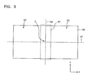
- FIG. 3 is a schematic plan view illustrating an organic light-emitting display apparatus according to another embodiment.
- FIG. 4 is a schematic plan view illustrating an example state of the organic light-emitting display apparatus illustrated in FIG. 3
- FIG. 5 is a schematic cross-sectional view illustrating a portion of the organic light-emitting display apparatus illustrated in FIG. 3 .
- the organic light-emitting display apparatus of FIGs. 3-5 includes a substrate 100, a plurality of first electrodes 210 separate from each other, a second electrode 250 disposed above the first electrodes 210 to face the first electrodes 210, an intermediate layer 230 including an emission layer and disposed between the first electrodes 210 and the second electrode 250, a first encapsulating layer 310, and a second encapsulating layer 320.
- the organic light-emitting display apparatus may further include a third encapsulating layer 330 as shown in FIG. 5 .
- the first encapsulating layer 310 may include an organic material
- the second encapsulating layer 320 may include an inorganic material.
- the shape of the first encapsulating layer 310 is different from the shape of the first encapsulating layer 310 of the organic light-emitting display apparatus of the embodiment described with reference to FIG. 1 .
- a portion of the first encapsulating layer 310 corresponding to a first region A1 of the substrate 100 is patterned in the form of a plurality of islands, and portions of the first encapsulating layer 310 corresponding to second regions A2 of the substrate 100 other than the first region A1 are formed as one body.
- the first encapsulating layer 310 may not be damaged.
- a region of the flexible substrate 100 which is mainly bent when the substrate 100 is subjected to bending may be defined as the first region A1, and in the first region A1, the first encapsulating layer 310 may be patterned in the form of a plurality of islands.
- the first encapsulating layer 310 may be formed as one body so as to rapidly manufacture the organic light-emitting display apparatus and reliably protect organic light-emitting devices disposed under the first encapsulating layer 310.
- the region A1 may include the center C of the substrate 100.
- the organic light-emitting display apparatus may be usually bent around the short axis SA passing through the center C of the substrate 100 as shown in FIG. 4 , and thus most bending may occur around the short axis SA passing through the center C of the substrate 100. Therefore, the first region A1 may include the center C of the substrate 100 and may extend along the short axis SA of the substrate 100.
- the first encapsulating layer 310 may be formed as one body in a +x direction from the first region A1 and in an -x display from the first region A1. That is, in the second regions A2, the first encapsulating layer 310 may be divided into two parts. That is, the number of the regions A2 is two, and the first encapsulating layer 310 is continuous in each of the regions A2.
- a first region A1 may include: a first portion P1 passing through the center C of a substrate 100 and extending along a short axis SA of the substrate 100; and a second portion P2 passing through the center of the substrate 100 and extending along a long axis LA of the substrate 100. That is, the first region A1 may have a + shape.
- the substrate 100 may include four second regions A2 divided by the first region A1.
- a first encapsulating layer 310 may be formed as one body in each of the second regions A2 and may be patterned in the form of a plurality of islands in the first region A1.
- the substrate 100 has the long axis LA and the short axis SA.
- the substrate 100 may have a square shape in a plan view.
- both sides of the substrate 100 may have a rectangular shape having two first edges extending in a first direction (+y direction) and two second edges extending in a second direction (+x direction) perpendicular to the first direction.
- the first portion P1 of the first region A1 may include the center C of the substrate 100 and extend in parallel with the first edges (in the +y direction)
- the second portion P2 of the first region A1 may include the center of the substrate 100 and extend in parallel with the second edges (in the +x direction). That is, the first region A1 may have a + shape.
- the first region A1 may be formed to include edges of the substrate 100.
- a first region A1 may include: a portion including the center C of a substrate 100 and extending in a short axis SA of the substrate 100; and a portion corresponding to edges of the substrate 100.
- the substrate 100 is flexible, if the edges of the substrate 100 are not supported by a structure such as a rigid frame, the edges of the substrate 100 may be bent more easily than other portions of the substrate 100 when a force or impactive force is intentionally or not intentionally applied to the substrate 100. Therefore, if the first region A1 includes the edges of the substrate 100, the durability of the organic light-emitting display apparatus may be improved.
- FIG. 8 is a schematic plan view illustrating an organic light-emitting display apparatus according to another embodiment.
- a first region A1 may correspond to only edges of a substrate 100.
- FIG. 9 is a schematic plan view illustrating an organic light-emitting display apparatus according to another embodiment.
- a substrate 100 may have a circular shape instead of a rectangular shape. In this case, a first region A1 may correspond to only the edge of the substrate 100.
- the islands of the first encapsulating layer 310 may correspond to the first electrodes 210 in the first region A1.
- the islands of the first encapsulating layer 310 may have different radii of curvature according to the wavelengths of light emitted from corresponding sub-pixels.
- the first electrodes 210 may include first color sub-pixel electrodes, second color sub-pixel electrodes, and third color sub-pixel electrodes.
- islands of the first encapsulating layer 310 corresponding to the first color sub-pixel electrodes may have a first radius of curvature
- islands of the first encapsulating layer 310 corresponding to the second color sub-pixel electrodes may have a second radius of curvature
- islands of the first encapsulating layer 310 corresponding to the third color sub-pixel electrodes may have a third radius of curvature.
- the first to third radii of curvature may be different from one another.
- the substrates 100 of the organic light-emitting display apparatuses are flexible. That is, the organic light-emitting display apparatuses are flexible organic light-emitting display apparatuses.
- a bendable substrate having a bending region may be used. In this case, a first region A1 may correspond to the bending region.
- a rigid substrate 100 may be used.
- the first encapsulating layer 310 is disposed on the second electrode 250.
- the embodiments of the present disclosure are not limited thereto.
- an encapsulating structure including organic and inorganic layers may be formed on the second electrode 250, and the first encapsulating layer 310 may be formed on the encapsulating structure.
- the organic light-emitting display apparatus may be durable and convenient to use.
- the embodiments are not limited thereto.
Landscapes
- Physics & Mathematics (AREA)
- Optics & Photonics (AREA)
- Chemical & Material Sciences (AREA)
- Inorganic Chemistry (AREA)
- Electroluminescent Light Sources (AREA)
Abstract
Description
- This application claims the benefit of Korean Patent Application No.
10-2014-0151585, filed on November 3, 2014 - One or more embodiments relate to a durable and convenient organic light-emitting display apparatus.
- Recent display apparatuses are used for various purposes, and owing to the development of slim and light display apparatuses, the use of display apparatuses has increased in more applications. Particularly, along with the rapid growth of the wearable device market, flexible display apparatuses have been actively developed.
- Flexible display apparatuses are bendable or flexible and thus may be conveniently used. Properties of substrates and various thin films of such flexible display apparatuses may have to be adjusted for guaranteeing the flexibility of the flexible display apparatuses.
- Typical display apparatuses do not have satisfactory flexibility, and if the display apparatuses are repeatedly used, the lifespans thereof are generally sharply decreased.
- One or more embodiments include a durable and convenient organic light-emitting display apparatus.
- Additional aspects will be set forth in part in the description which follows and, in part, will be apparent from the description, or may be learned by practice of the presented embodiments.
- According to one or more embodiments, an organic light-emitting display apparatus includes: a substrate; first electrodes arranged separate from one another on the substrate; a second electrode disposed above the first electrodes to face the first electrodes; an intermediate layer disposed between the first electrodes and the second electrode and including an emission layer; a first encapsulating layer disposed on the second electrode wherein at least a portion of the first encapsulating layer is patterned to have a plurality of islands, the first encapsulating layer including an organic material; and a second encapsulating layer covering the islands of the first encapsulating layer and including an inorganic material.
- The islands of the first encapsulating layer may correspond to the first electrodes. The first electrodes may include first color sub-pixel electrodes, second color sub-pixel electrodes, and third color sub-pixel electrodes, wherein islands of the first encapsulating layer corresponding to the first color sub-pixel electrodes may have a first radius of curvature, islands of the first encapsulating layer corresponding to the second color sub-pixel electrodes may have a second radius of curvature, and islands of the first encapsulating layer corresponding to the third color sub-pixel electrodes may have a third radius of curvature.
- According to one or more embodiments, an organic light-emitting display apparatus includes: a substrate; first electrodes arranged separate from one another; a second electrode disposed above the first electrodes to face the first electrodes; an intermediate layer disposed between the first electrodes and the second electrode and including an emission layer; a first encapsulating layer disposed on the second electrode, wherein a portion of the first encapsulating layer corresponding to a first region of the substrate is patterned to have a plurality of islands, and a portion of the first encapsulating layer corresponding to a second region of the substrate is formed as one body; and a second encapsulating layer covering the first encapsulating layer.
- The first encapsulating layer may include an organic material, and the second encapsulating layer may include an inorganic material.
- The substrate may be a bendable substrate including a bending region, and the first region may correspond to the bending region.
- The substrate may be a flexible substrate, and the first region may include a center of the substrate. The substrate may include a long axis and a short axis, and the first region may include the center of the substrate and may extend along the short axis of the substrate.
- Both sides of the substrate may have a rectangular shape including first edges extending in a first direction and second edges extending in a second direction perpendicular to the first direction, wherein the first region may include: a first portion including the center of the substrate and extending in a direction parallel to the first edges; and a second portion including the center of the substrate and extending in a direction parallel to the second edges.
- The first region may include an edge of the substrate.
- The first region may correspond to an edge of the substrate. The substrate may be circular shaped.
- The second encapsulating layer may be formed as one body.
- The organic light-emitting display apparatus may further include a third encapsulating layer covering the second encapsulating layer and including an organic material.
- The islands of the first encapsulating layer may correspond to the first electrodes in the first region. The first electrodes may include first color sub-pixel electrodes, second color sub-pixel electrodes, and third color sub-pixel electrodes, wherein islands of the first encapsulating layer corresponding to the first color sub-pixel electrodes may have a first radius of curvature, islands of the first encapsulating layer corresponding to the second color sub-pixel electrodes may have a second radius of curvature, and islands of the first encapsulating layer corresponding to the third color sub-pixel electrodes may have a third radius of curvature.
- These and/or other aspects will become apparent and more readily appreciated from the following description of certain embodiments, taken in conjunction with the accompanying drawings in which:
-
FIG. 1 is a schematic cross-sectional view illustrating a portion of an organic light-emitting display apparatus according to an embodiment; -
FIG. 2 is a schematic cross-sectional view illustrating a portion of an organic light-emitting display apparatus according to another embodiment; -
FIG. 3 is a schematic plan view illustrating an organic light-emitting display apparatus according to another embodiment; -
FIG. 4 is a schematic plan view illustrating an example state of the organic light-emitting display apparatus illustrated inFIG. 3 ; -
FIG. 5 is a schematic cross-sectional view illustrating a portion of the organic light-emitting display apparatus illustrated inFIG. 3 ; -
FIG. 6 is a schematic plan view illustrating an organic light-emitting display apparatus according to another embodiment; -
FIG. 7 is a schematic plan view illustrating an organic light-emitting display apparatus according to another embodiment; -
FIG. 8 is a schematic plan view illustrating an organic light-emitting display apparatus according to another embodiment; and -
FIG. 9 is a schematic plan view illustrating an organic light-emitting display apparatus according to another embodiment. - Reference will now be made in detail to certain embodiments, examples of which are illustrated in the accompanying drawings. Effects and features of the embodiments, and implementation methods thereof will be clarified through the following descriptions given with reference to the accompanying drawings. In this regard, the embodiments may have different forms and should not be construed as being limited to the descriptions set forth herein. As used herein, the term "and/or" includes any and all combinations of one or more of the associated listed items.
- Hereinafter, the embodiments will be described in detail with reference to the accompanying drawings. In the drawings, like reference numerals generally denote like elements, and overlapping descriptions thereof will be omitted.
- It will be understood that when a layer, a film, a region, or a plate is referred to as being "on" or "above" another layer, film, region, or plate, it can be directly on the other layer, film, region, or plate, or intervening layers, films, regions, or plates may also be present. In addition, sizes of elements in the drawings may be exaggerated for convenience of explanation. In other words, since sizes and thicknesses of components in the drawings are arbitrarily illustrated for convenience of explanation, the following embodiments are not limited thereto.
- In the following examples, the x-axis, the y-axis and the z-axis are not limited to three axes of the rectangular coordinate system, and may be interpreted in a broader sense. For example, the x-axis, the y-axis, and the z-axis may be perpendicular to one another, or may represent different directions that are not perpendicular to one another.
-
FIG. 1 is a schematic cross-sectional view illustrating a portion of an organic light-emitting display apparatus according to an embodiment. - Referring to
FIG. 1 , the organic light-emitting display apparatus includes asubstrate 100, thin-film transistors TFT, capacitors Cap, abuffer layer 110, agate insulating layer 130, aninterlayer insulating layer 150, aplanarization layer 170,first electrodes 210, anintermediate layer 230, asecond electrode 250, a firstencapsulating layer 310, and a secondencapsulating layer 320. - The
substrate 100 may be a flexible substrate including a plastic material. However, if thesubstrate 100 contains a plastic material, moisture or oxygen may more easily permeate thesubstrate 100 than with a glass substrate, and thus organic light-emitting devices vulnerable to moisture or oxygen may be degraded and shortened in lifespan. To prevent this, thebuffer layer 110 having a single-layer or multi-layer structure including a silicon oxide or silicon nitride may be disposed on thesubstrate 100. - The thin-film transistors TFT and organic light-emitting devices may be disposed on the
buffer layer 110. The organic light-emitting devices may include thefirst electrodes 210, theintermediate layer 230, and thesecond electrode 250. - The thin-film transistors TFT may include gate electrodes, source electrodes, drain electrodes, and a semiconductor layer. The
gate insulating layer 130 may include a silicon oxide or silicon nitride and be disposed between the semiconductor layer and the gate electrodes for insulating the semiconductor layer from the gate electrodes. Theinterlayer insulating layer 150 may be disposed on the gate electrodes. Theinterlayer insulating layer 150 may have a single-layer or multi-layer structure including a material such as, for example, a silicon oxide or silicon nitride. However, a material that may be used for forming theinterlayer insulating layer 150 is not limited thereto. That is, various materials may be used for forming theinterlayer insulating layer 150. This is the same for other elements. The source electrodes and the drain electrodes are formed on theinterlayer insulating layer 150. The source electrodes and the drain electrodes are electrically connected to the semiconductor layer through contact holes formed in theinterlayer insulating layer 150 and thegate insulating layer 130. - In the thin-film transistors TFT illustrated in
FIG. 1 , the semiconductor layer forms a lowermost layer, the gate electrodes are formed above the semiconductor layer, and the source electrodes and the drain electrodes form an uppermost layer. However, the thin-film transistors TFT may have a different structure. The semiconductor layer may include a poly-silicon layer, an amorphous silicon layer, an organic semiconductor layer, or a conductive oxide semiconductor layer. - A protective layer or the
planarization layer 170 may be disposed on the source electrodes and the drain electrodes so as to protect or flatten the lower thin-film transistors TFT. The protective layer or theplanarization layer 170 may be formed by various methods. For example, the protective layer or theplanarization layer 170 may include an organic material such as, for example, benzocyclobutene (BCB) or acrylic, or an inorganic material such as, for example, a silicon oxide or silicon nitride. The protective layer or theplanarization layer 170 may have a single-layer structure, a double-layer structure, or a multi-layer structure. - The organic light-emitting devices may be disposed on the protective layer or the
planarization layer 170. The organic light-emitting devices include thefirst electrodes 210 as pixel electrodes, thesecond electrode 250 as an opposite electrode facing thefirst electrodes 210, and theintermediate layer 230 including at least an emission layer, and disposed between thefirst electrodes 210 and thesecond electrode 250. Apixel defining layer 180 covers thefirst electrodes 210 except for regions including center regions of thefirst electrodes 210 so that thefirst electrodes 210 may be exposed through the regions. - The
first electrodes 210 being pixel electrodes are anodes, and thesecond electrode 250 being an opposite electrode is a cathode. However, the polarities of the first electrodes 210 (pixel electrodes) and the second electrode 250 (opposite electrode) may be opposite to this configuration in other embodiments. - The
first electrodes 210 may be transparent or reflective electrodes. If thefirst electrodes 210 are transparent electrodes, thefirst electrodes 210 may include, for example, ITO, IZO, ZnO, or In2O3. If thefirst electrodes 210 are reflective electrodes, each of thefirst electrodes 210 may include: a reflective layer including silver (Ag), magnesium (Mg), aluminum (Al), platinum (Pt), palladium (Pd), gold (Au), nickel (Ni), neodymium (Nd), iridium (Ir), chromium (Cr), or a compound thereof; and a ITO, IZO, ZnO, or In2O3 layer formed on the reflective layer. - Similarly, the
second electrode 250 may be a transparent or reflective electrode. If thesecond electrode 250 is a transparent electrode, thesecond electrode 250 may include: a deposition layer facing thefirst electrodes 210 and including lithium (Li), calcium (Ca), LiF/Ca, LiF/Al, aluminum (Al), magnesium (Mg), or a compound thereof; and auxiliary electrodes or bus electrode lines including a material used to form transparent electrodes such as, for example, ITO, IZO, ZnO, or In2O3. If thesecond electrode 250 is a reflective electrode, thesecond electrode 250 may include a deposition layer including Li, Ca, LiF/Ca, LiF/Al, Al, Mg, or a compound thereof. - The
intermediate layer 230 including at least an emission layer is disposed between thefirst electrodes 210 and thesecond electrode 250. Theintermediate layer 230 may include a low molecular organic material or a high molecular organic material. - If the
intermediate layer 230 includes a low molecular organic material, theintermediate layer 230 may have a stacked structure including a hole injection layer (HIL), an organic emission layer (EML), an electron transport layer (ETL), and an electron injection layer (EIL). In this case, theintermediate layer 230 may include an organic material such as, for example, copper phthalocyanine (CuPc), N,N'-Di(naphthalene-1-yl)-N,N'-diphenyl-benzidine (NPB), or tris-8-hydroxyquinoline aluminum (Alq3). The layers including a low molecular organic material may be formed by a method such as a vacuum deposition method using masks, for example. - If the
intermediate layer 230 includes a high molecular organic material, theintermediate layer 230 may have a structure including a hole transport layer (HTL) and an emission layer (EML). In this case, the hole transport layer may include PEDOT, and the emission layer may include a high molecular organic material such as, for example, a poly-phenylenevinylene (PPV)-containing organic material or a polyfluorene-containing organic material. - The
intermediate layer 230 including an emission layer may emit red, green, or blue light. A sub-pixel may be a region capable of emitting red, green, or blue light, and in this case, a group constituted by three sub-pixels may form a pixel. In another example, a sub-pixel may emit light having a color other than red, green, and blue. That is, a pixel may be constituted by a plurality of sub-pixels emitting light of different colors as long as the pixel may emit white light. In another example, all sub-pixels may emit white light, and light emitted from the sub-pixels may pass through a color conversion layer or color filters. - In
FIG. 1 , theintermediate layer 230 is illustrated as being patterned to correspond to thefirst electrodes 210. This is for illustrative purposes only. For example, a layer of theintermediate layer 230, such as a hole injection layer, may be formed as one body to substantially correspond to an entire surface of thesubstrate 100, and another layer of theintermediate layer 230, such as an emission layer, may be patterned to correspond to thefirst electrodes 210. - The organic light-emitting devices are arranged on the
substrate 100, and thefirst electrodes 210 are accordingly arranged on thesubstrate 100. Thesecond electrode 250 is formed as one body in a display region to correspond to thefirst electrodes 210. - The
first encapsulating layer 310 is formed on thesecond electrode 250. As shown inFIG. 1 , thefirst encapsulating layer 310 is patterned to form a plurality of islands separate from each other. Thefirst encapsulating layer 310 includes an organic material. Thesecond encapsulating layer 320 includes an inorganic material and covers the islands of thefirst encapsulating layer 310. Thesecond encapsulating layer 320 may cover almost all of the area of thesubstrate 100 and may be formed as one body. If necessary, athird encapsulating layer 330 including an organic material may be formed to cover thesecond encapsulating layer 320. For example, thefirst encapsulating layer 310 may include polyethylene terephthalate, polyethylene naphthalate, polycarbonate, polyimide, polyethylene sulfonate, polyoxymethylene, and/or polyarylate. Thesecond encapsulating layer 320 may include a silicon oxide, silicon nitride, or aluminum oxide. - The
first encapsulating layer 310 and thesecond encapsulating layer 320 are thin-film encapsulating layers for protecting the organic light-emitting devices from impacts or impurities. - In an organic light-emitting display apparatus, a thin-film encapsulating layer may be formed by alternately forming inorganic and organic layers. Such a thin-film encapsulating layer may be formed on the entirety of a surface of a panel by a deposition method. If a panel of a flexible display apparatus on which a thin-film encapsulating layer is entirely formed without any discontinuous portions as described above is twisted or bent, although the thickness of the thin-film encapsulating layer is small as compared with the thickness of the flexible display apparatus, a region of the thin-film encapsulating layer in which stress is concentrated is frequently cracked. Moreover, if cracks grow, the durability of the panel may be markedly affected.
- However, in the organic light-emitting display apparatus of the disclosed embodiment, the
first encapsulating layer 310 disposed on thesecond electrode 250 is patterned in the form of a plurality of separate islands. Although thefirst encapsulating layer 310 patterned in the form of separate islands is twisted or bent in any direction by applying any amount of force, each island having a small size may not be readily cracked. In addition, although cracks are formed in some of the islands of thefirst encapsulating layer 310, the cracks do not propagate to neighboring islands. Therefore, according to the described embodiment, the generation of defects may be easily prevented in manufacturing processes of the organic light-emitting display apparatus, and thin-film encapsulation durable to bending or twisting may be guaranteed in the organic light-emitting display apparatus. Therefore, the organic light-emitting display apparatus may have high flexibility. - In addition, since the
first encapsulating layer 310 including an organic material is patterned in the form of separate islands, when structures such as thesubstrate 100 are bent, stress generated in the thin-film encapsulating layers are absorbed in thefirst encapsulating layer 310. As a result, when thesubstrate 100 is bent, thesecond encapsulating layer 320 covering thefirst encapsulating layer 310 may be subjected to less stress. Therefore, thesecond encapsulating layer 320 including an inorganic material may not be damaged or may be less damaged. - The
first encapsulating layer 310 may be easily patterned in the form of separate islands by a method such as an inkjet printing. That is, thefirst encapsulating layer 310 may be easily patterned in the form of separate islands by dotting thesecond electrode 250 with a monomer at separate positions by an inkjet printing method, and curing the monomer. In this case, the upper surface of thesecond electrode 250 may be hydrophobically-treated, for example, through a plasma process, so as to prevent dots formed by inkjet printing from spreading and meeting each other. - As shown in
FIG. 1 , since the islands of thefirst encapsulating layer 310 correspond to thefirst electrodes 210, the flexibility of the organic light-emitting display apparatus may be markedly improved, and durable thin-film encapsulation may be realized. In the organic light-emitting display apparatus, since thefirst electrodes 210, which are pixel electrodes, are formed by performing a patterning process in units of sub-pixels, thefirst electrodes 210 are not highly flexible. Therefore, thefirst encapsulating layer 310 may be patterned in units of sub-pixels (that is, thefirst encapsulating layer 310 may be patterned to correspond to the first electrodes 210) so as to maximize the flexibility of the organic light-emitting display apparatus. In addition, since thefirst encapsulating layer 310 is patterned, although the organic light-emitting display apparatus is bent, the formation of cracks in thefirst encapsulating layer 310 may be prevented or markedly reduced. This will be the same in the embodiments and modification examples described below. -
FIG. 2 is a schematic cross-sectional view illustrating a portion of an organic light-emitting display apparatus according to another embodiment. In the organic light-emitting display apparatus ofFIG. 2 , the shape of afirst encapsulating layer 310 is different from the shape of thefirst encapsulating layer 310 of the organic light-emitting display apparatus described with reference toFIG. 1 . In the organic light-emitting display apparatus ofFIG. 2 , a plurality offirst electrodes 210 may include first color sub-pixel electrodes, second color sub-pixel electrodes, and third color sub-pixel electrodes. For example, if the organic light-emitting display apparatus includes red sub-pixels R, green sub-pixels G, and blue sub-pixels B, the red sub-pixels R may correspond to the first color sub-pixel electrodes of thefirst electrodes 210, the green sub-pixels G may correspond to the second color sub-pixel electrodes of thefirst electrodes 210, and the blue sub-pixels B may correspond to the third color sub-pixel electrodes of thefirst electrodes 210. - In this case, some islands of the
first encapsulating layer 310 corresponding to the first color sub-pixel electrodes may have a first radius of curvature, other islands of thefirst encapsulating layer 310 corresponding to the second color sub-pixel electrodes may have a second radius of curvature, and the other islands of thefirst encapsulating layer 310 corresponding to the third color sub-pixel electrodes may have a third radius of curvature. The first to third radii of curvature may be different from one another. - The islands of the
first encapsulating layer 310 may be shaped like a convex lens. The islands of thefirst encapsulating layer 310 corresponding to thefirst electrodes 210 may be formed to function as convex lenses by using refractive index differences between thefirst encapsulating layer 310 and asecond encapsulating layer 320, so as to improve the light extraction efficiency and front-side brightness of the organic light-emitting display apparatus. In this case, the radii of curvature of the convex lenses may be differently adjusted according to the wavelengths of light emitted from an emission layer so as to improve the light extraction efficiency and brightness of each sub-pixel. - For example, when the same electric signal is applied to a red sub-pixel R, a green sub-pixel G, and a blue sub-pixel B, the optical efficiency of a blue emission layer of the blue sub-pixel B may be lowest, and the optical efficiency of a green emission layer of the green sub-pixel G may be highest. In this case, as shown in
FIG. 2 , anisland 310B of thefirst encapsulating layer 310 corresponding to the blue sub-pixel B may be formed to have the largest radius of curvature, and anisland 310G of thefirst encapsulating layer 310 corresponding to the green sub-pixel G may be formed to have the smallest radius of curvature. In this manner, although differences between electric signals applied to the red sub-pixel R, the green sub-pixel G, and the blue sub-pixel B are reduced, the degrees of brightness of light emitted from the red sub-pixel R, the green sub-pixel G, and the blue sub-pixel B may be adjusted to be similar to each other. For example, anisland 310R of thefirst encapsulating layer 310 corresponding to the red sub-pixel R may have a radius of curvature of about 27.2 µm, theisland 310G of thefirst encapsulating layer 310 corresponding to the green sub-pixel G may have a radius of curvature of about 17.5 µm, and theisland 310B of thefirst encapsulating layer 310 corresponding to the blue sub-pixel B may have a radius of curvature of about 28.6 µm. -
FIG. 3 is a schematic plan view illustrating an organic light-emitting display apparatus according to another embodiment.FIG. 4 is a schematic plan view illustrating an example state of the organic light-emitting display apparatus illustrated inFIG. 3 , andFIG. 5 is a schematic cross-sectional view illustrating a portion of the organic light-emitting display apparatus illustrated inFIG. 3 . - Like the organic light-emitting display apparatus of the previous embodiment described with reference to
FIG. 1 , the organic light-emitting display apparatus ofFIGs. 3-5 includes asubstrate 100, a plurality offirst electrodes 210 separate from each other, asecond electrode 250 disposed above thefirst electrodes 210 to face thefirst electrodes 210, anintermediate layer 230 including an emission layer and disposed between thefirst electrodes 210 and thesecond electrode 250, afirst encapsulating layer 310, and asecond encapsulating layer 320. In addition, the organic light-emitting display apparatus may further include athird encapsulating layer 330 as shown inFIG. 5 . Thefirst encapsulating layer 310 may include an organic material, and thesecond encapsulating layer 320 may include an inorganic material. - However, the shape of the
first encapsulating layer 310 is different from the shape of thefirst encapsulating layer 310 of the organic light-emitting display apparatus of the embodiment described with reference toFIG. 1 . In the organic light-emitting display apparatus ofFIGs. 3-5 , a portion of thefirst encapsulating layer 310 corresponding to a first region A1 of thesubstrate 100 is patterned in the form of a plurality of islands, and portions of thefirst encapsulating layer 310 corresponding to second regions A2 of thesubstrate 100 other than the first region A1 are formed as one body. - As described above, if the
first encapsulating layer 310 is patterned in the form of a plurality of islands, although the substrate (flexible substrate) 100 is bent, thefirst encapsulating layer 310 may not be damaged. For this, a region of theflexible substrate 100 which is mainly bent when thesubstrate 100 is subjected to bending may be defined as the first region A1, and in the first region A1, thefirst encapsulating layer 310 may be patterned in the form of a plurality of islands. In the second regions A2 other than the first region A1, thefirst encapsulating layer 310 may be formed as one body so as to rapidly manufacture the organic light-emitting display apparatus and reliably protect organic light-emitting devices disposed under thefirst encapsulating layer 310. - When the
flexible substrate 100 is bent, a region around the center C of thesubstrate 100 may be mostly bent. Therefore, the region A1 may include the center C of thesubstrate 100. - If the
flexible substrate 100 has a long axis LA and a short axis SA as shown inFIG. 3 , the organic light-emitting display apparatus may be usually bent around the short axis SA passing through the center C of thesubstrate 100 as shown inFIG. 4 , and thus most bending may occur around the short axis SA passing through the center C of thesubstrate 100. Therefore, the first region A1 may include the center C of thesubstrate 100 and may extend along the short axis SA of thesubstrate 100. - In this case, the
first encapsulating layer 310 may be formed as one body in a +x direction from the first region A1 and in an -x display from the first region A1. That is, in the second regions A2, thefirst encapsulating layer 310 may be divided into two parts. That is, the number of the regions A2 is two, and thefirst encapsulating layer 310 is continuous in each of the regions A2. - Referring to
FIG. 6 schematically illustrating an organic light-emitting display apparatus according to another embodiment, a first region A1 may include: a first portion P1 passing through the center C of asubstrate 100 and extending along a short axis SA of thesubstrate 100; and a second portion P2 passing through the center of thesubstrate 100 and extending along a long axis LA of thesubstrate 100. That is, the first region A1 may have a + shape. In this case, thesubstrate 100 may include four second regions A2 divided by the first region A1. Afirst encapsulating layer 310 may be formed as one body in each of the second regions A2 and may be patterned in the form of a plurality of islands in the first region A1. - In
FIG. 6 , thesubstrate 100 has the long axis LA and the short axis SA. However, the embodiments of the present disclosure are not limited thereto. For example, thesubstrate 100 may have a square shape in a plan view. In any case, both sides of thesubstrate 100 may have a rectangular shape having two first edges extending in a first direction (+y direction) and two second edges extending in a second direction (+x direction) perpendicular to the first direction. In this case, the first portion P1 of the first region A1 may include the center C of thesubstrate 100 and extend in parallel with the first edges (in the +y direction), and the second portion P2 of the first region A1 may include the center of thesubstrate 100 and extend in parallel with the second edges (in the +x direction). That is, the first region A1 may have a + shape. - The first region A1 may be formed to include edges of the
substrate 100. For example, referring toFIG. 7 illustrating a modification example of the organic light-emitting display apparatus illustrated inFIG. 3 , a first region A1 may include: a portion including the center C of asubstrate 100 and extending in a short axis SA of thesubstrate 100; and a portion corresponding to edges of thesubstrate 100. When thesubstrate 100 is flexible, if the edges of thesubstrate 100 are not supported by a structure such as a rigid frame, the edges of thesubstrate 100 may be bent more easily than other portions of thesubstrate 100 when a force or impactive force is intentionally or not intentionally applied to thesubstrate 100. Therefore, if the first region A1 includes the edges of thesubstrate 100, the durability of the organic light-emitting display apparatus may be improved. -
FIG. 8 is a schematic plan view illustrating an organic light-emitting display apparatus according to another embodiment. Referring toFIG. 8 , a first region A1 may correspond to only edges of asubstrate 100.FIG. 9 is a schematic plan view illustrating an organic light-emitting display apparatus according to another embodiment. Referring toFIG. 9 , asubstrate 100 may have a circular shape instead of a rectangular shape. In this case, a first region A1 may correspond to only the edge of thesubstrate 100. - In each of the embodiments described with reference to
FIGS. 3 to 9 , the islands of thefirst encapsulating layer 310 may correspond to thefirst electrodes 210 in the first region A1. In addition, as described with reference toFIG. 2 , in each of the embodiments described with reference toFIGS. 3 to 9 , the islands of thefirst encapsulating layer 310 may have different radii of curvature according to the wavelengths of light emitted from corresponding sub-pixels. For example, thefirst electrodes 210 may include first color sub-pixel electrodes, second color sub-pixel electrodes, and third color sub-pixel electrodes. In this case, islands of thefirst encapsulating layer 310 corresponding to the first color sub-pixel electrodes may have a first radius of curvature, islands of thefirst encapsulating layer 310 corresponding to the second color sub-pixel electrodes may have a second radius of curvature, and islands of thefirst encapsulating layer 310 corresponding to the third color sub-pixel electrodes may have a third radius of curvature. The first to third radii of curvature may be different from one another. - In the descriptions of
FIGS. 3 to 9 , thesubstrates 100 of the organic light-emitting display apparatuses are flexible. That is, the organic light-emitting display apparatuses are flexible organic light-emitting display apparatuses. However, in other embodiments, a bendable substrate having a bending region may be used. In this case, a first region A1 may correspond to the bending region. Furthermore, in other embodiments, arigid substrate 100 may be used. - In the description given above, the
first encapsulating layer 310 is disposed on thesecond electrode 250. However, the embodiments of the present disclosure are not limited thereto. For example, an encapsulating structure including organic and inorganic layers may be formed on thesecond electrode 250, and thefirst encapsulating layer 310 may be formed on the encapsulating structure. - As described above, according to the one or more of the above embodiments, the organic light-emitting display apparatus may be durable and convenient to use. However, the embodiments are not limited thereto.
- It should be understood that the embodiments described herein should be considered in a descriptive sense only and not for purposes of limitation. Descriptions of features or aspects within each embodiment should typically be considered as available for other similar features or aspects in other embodiments.
- While certain embodiments have been described with reference to the figures, it will be understood by those of ordinary skill in the art that various changes in form and details may be made therein without departing from the spirit and scope as defined by the following claims.
Claims (15)
- An organic light-emitting display apparatus comprising:a substrate (100);first electrodes (210) arranged separate from one another on the substrate (100);a second electrode (250) disposed above the first electrodes (210) to face the first electrodes;an intermediate layer (230) disposed between the first electrodes (210) and the second electrode (250) and comprising an emission layer;a first encapsulating layer (310) disposed on the second electrode (250), wherein at least a portion of the first encapsulating layer (310) is patterned to have a plurality of islands, the first encapsulating layer (310) comprising an organic material; anda second encapsulating layer (320) covering the islands of the first encapsulating layer (310) and comprising an inorganic material.
- The organic light-emitting display apparatus of claim 1, wherein the islands of the first encapsulating layer (310) correspond to the first electrodes (210).
- The organic light-emitting display apparatus of claim 2, wherein the first electrodes (210) comprise first color sub-pixel electrodes, second color sub-pixel electrodes, and third color sub-pixel electrodes.
- The organic light-emitting display apparatus of claim 3, wherein islands of the first encapsulating layer (310) correspond to the first color sub-pixel electrodes, the second color sub-pixel electrodes and the third color sub-pixel electrodes.
- The organic light-emitting display apparatus of claim 4, wherein islands of the first encapsulating layer (310R) corresponding to the first color sub-pixel electrodes have a first radius of curvature, islands of the first encapsulating layer (310G) corresponding to the second color sub-pixel electrodes have a second radius of curvature, and islands of the first encapsulating layer (310B) corresponding to the third color sub-pixel electrodes have a third radius of curvature.
- The organic light-emitting display apparatus of one of the preceding claims further comprising:wherein the portion of the first encapsulating layer (310) corresponds to a first region (A1) of the substrate (100), and a disjoint further portion of the first encapsulating layer (310) corresponding to a second region (A2) of the substrate (100) is formed as one body.
- The organic light-emitting display apparatus of claim 5, wherein the substrate (100) is a bendable substrate comprising a bending region, and the first region (A1) corresponds to the bending region.
- The organic light-emitting display apparatus of claim 5, wherein the substrate (100) is a flexible substrate, and the first region comprises a center (C) of the substrate (100).
- The organic light-emitting display apparatus of claim8, wherein the substrate (100) comprises a long axis (LA) and a short axis (SA), and the first region (A1) comprises the center of the substrate (100) and extends along the short axis (SA) of the substrate (100).
- The organic light-emitting display apparatus of claim8, wherein the substrate (100) has a rectangular shape and comprises first edges extending in a first direction (x) and second edges extending in a second direction (y) perpendicular to the first direction (x),
wherein the first region (A1) comprises:a first portion (P1) comprising the center (C) of the substrate (100) and extending in a direction parallel to the first edges; anda second portion (P2) comprising the center (C)of the substrate (100) and extending in a direction parallel to the second edges. - The organic light-emitting display apparatus of claim 7, wherein the first region (A1) comprises an edge of the substrate (100).
- The organic light-emitting display apparatus of claim 7, wherein the first region (A1) corresponds to an edge of the substrate (100).
- The organic light-emitting display apparatus of claim 12, wherein the substrate (100) is circular shaped.
- The organic light-emitting display apparatus of one of the preceding claims, wherein the second encapsulating layer (320) is formed as one body.
- The organic light-emitting display apparatus of one of the preceding claims, further comprising a third encapsulating layer (330) covering the second encapsulating layer (320) and comprising an organic material.
Applications Claiming Priority (1)
| Application Number | Priority Date | Filing Date | Title |
|---|---|---|---|
| KR1020140151585A KR102352283B1 (en) | 2014-11-03 | 2014-11-03 | Organic light-emitting display apparatus |
Publications (2)
| Publication Number | Publication Date |
|---|---|
| EP3016166A1 true EP3016166A1 (en) | 2016-05-04 |
| EP3016166B1 EP3016166B1 (en) | 2019-12-11 |
Family
ID=54360306
Family Applications (1)
| Application Number | Title | Priority Date | Filing Date |
|---|---|---|---|
| EP15191679.8A Active EP3016166B1 (en) | 2014-11-03 | 2015-10-27 | Organic light-emitting display apparatus |
Country Status (4)
| Country | Link |
|---|---|
| US (2) | US10727442B2 (en) |
| EP (1) | EP3016166B1 (en) |
| KR (1) | KR102352283B1 (en) |
| CN (1) | CN105576000B (en) |
Cited By (5)
| Publication number | Priority date | Publication date | Assignee | Title |
|---|---|---|---|---|
| CN110534664A (en) * | 2019-09-11 | 2019-12-03 | 昆山国显光电有限公司 | The production method and display device of a kind of display panel, display panel |
| CN112002734A (en) * | 2020-08-06 | 2020-11-27 | 武汉华星光电半导体显示技术有限公司 | OLED display panel |
| EP3951567A4 (en) * | 2019-03-28 | 2022-06-15 | Ningbo Sunny Opotech Co., Ltd. | TERMINAL DEVICE AND ASSOCIATED DISPLAY SCREEN, AND DISPLAY SCREEN PREPARATION METHOD |
| CN117765884A (en) * | 2022-09-23 | 2024-03-26 | 北京京东方技术开发有限公司 | Display panels and display devices |
| US12713775B2 (en) | 2022-09-23 | 2026-08-18 | Beijing Boe Technology Development Co., Ltd. | Display panel and display apparatus |
Families Citing this family (46)
| Publication number | Priority date | Publication date | Assignee | Title |
|---|---|---|---|---|
| KR102359349B1 (en) * | 2015-02-03 | 2022-02-07 | 삼성디스플레이 주식회사 | Organic light emitting diode display |
| KR102505878B1 (en) * | 2016-01-29 | 2023-03-06 | 삼성디스플레이 주식회사 | Flexible display apparatus |
| KR20180005323A (en) * | 2016-07-05 | 2018-01-16 | 삼성디스플레이 주식회사 | Organic light-emitting display apparatus |
| KR102556022B1 (en) | 2016-07-06 | 2023-07-17 | 삼성디스플레이 주식회사 | Flexible display device |
| CN107046047A (en) * | 2016-08-19 | 2017-08-15 | 广东聚华印刷显示技术有限公司 | Pixel cell of printed form electroluminescent device and its preparation method and application |
| KR102649240B1 (en) | 2016-08-23 | 2024-03-21 | 삼성디스플레이 주식회사 | Display device and manufacturing method of the same |
| KR102671042B1 (en) * | 2016-09-06 | 2024-06-03 | 삼성디스플레이 주식회사 | Display apparatus |
| CN107026239B (en) * | 2016-09-22 | 2019-08-09 | 广东聚华印刷显示技术有限公司 | Organic electroluminescence device and its preparation method and application |
| KR102448066B1 (en) * | 2017-12-22 | 2022-09-28 | 엘지디스플레이 주식회사 | flexible display device |
| KR102495845B1 (en) | 2017-12-26 | 2023-02-06 | 삼성디스플레이 주식회사 | Display apparatus |
| CN108288680B (en) * | 2017-12-29 | 2020-09-08 | 信利(惠州)智能显示有限公司 | Flexible AMOLED display screen packaging structure and packaging method thereof |
| KR102576997B1 (en) * | 2017-12-29 | 2023-09-12 | 삼성디스플레이 주식회사 | Display device and method of manufacturing display device |
| WO2019222405A1 (en) * | 2018-05-18 | 2019-11-21 | Corning Incorporated | Light extraction apparatus and flexible oled displays |
| KR102333769B1 (en) * | 2018-06-29 | 2021-12-01 | 삼성디스플레이 주식회사 | Display device |
| CN109192878B (en) * | 2018-08-30 | 2019-11-26 | 武汉华星光电半导体显示技术有限公司 | Flexible OLED display panel |
| CN109148723B (en) * | 2018-08-30 | 2021-03-30 | 上海天马微电子有限公司 | Display panel and preparation method thereof |
| CN109300939B (en) * | 2018-08-30 | 2022-02-01 | 云谷(固安)科技有限公司 | Flexible display panel, preparation method thereof, and display device |
| CN109616492B (en) * | 2018-10-26 | 2020-11-06 | 武汉华星光电半导体显示技术有限公司 | Flexible display panel, flexible display device and manufacturing method of flexible display panel |
| KR102745474B1 (en) * | 2018-11-16 | 2024-12-20 | 엘지디스플레이 주식회사 | Organic light emitting display device display device |
| KR102607212B1 (en) * | 2018-11-22 | 2023-11-28 | 엘지디스플레이 주식회사 | Flexible display apparatus |
| US11296156B2 (en) | 2018-11-28 | 2022-04-05 | Lg Display Co., Ltd. | Organic light emitting diode device |
| KR102696416B1 (en) * | 2018-12-05 | 2024-08-16 | 엘지디스플레이 주식회사 | Electroluminescent Display Apparatus |
| CN109686862A (en) * | 2019-01-10 | 2019-04-26 | 武汉华星光电半导体显示技术有限公司 | Display panel |
| US10892257B2 (en) * | 2019-01-21 | 2021-01-12 | Innolux Corporation | Foldable display device |
| KR102707560B1 (en) * | 2019-05-27 | 2024-09-20 | 삼성디스플레이 주식회사 | Display apparatus and the manufacturing method thereof |
| KR102872907B1 (en) * | 2019-07-02 | 2025-10-17 | 삼성디스플레이 주식회사 | Display device |
| CN110504385B (en) * | 2019-08-29 | 2022-04-15 | 京东方科技集团股份有限公司 | Display panel, manufacturing method thereof and display device |
| CN110767734A (en) * | 2019-10-31 | 2020-02-07 | 武汉天马微电子有限公司 | Display panel, display device and manufacturing method of display panel |
| US11211439B2 (en) * | 2019-11-27 | 2021-12-28 | Applied Materials, Inc. | Stretchable polymer and dielectric layers for electronic displays |
| WO2021146077A1 (en) | 2020-01-17 | 2021-07-22 | Corning Incorporated | Reduced coating diameter chlorine-doped silica optical fibers with low loss and microbend sensitivity |
| CN111223909A (en) * | 2020-03-18 | 2020-06-02 | 深圳市华星光电半导体显示技术有限公司 | Display panel and preparation method thereof |
| CN111509141B (en) * | 2020-05-06 | 2023-08-01 | 上海天马微电子有限公司 | Display panel, manufacturing method thereof, and display device |
| CN111584739B (en) * | 2020-05-08 | 2022-07-12 | 武汉华星光电半导体显示技术有限公司 | OLED display panel, preparation method thereof and OLED display device |
| CN111768706A (en) * | 2020-06-24 | 2020-10-13 | 武汉华星光电半导体显示技术有限公司 | A display panel, its manufacturing method and display device |
| CN111864112B (en) * | 2020-07-22 | 2022-06-10 | 武汉华星光电半导体显示技术有限公司 | Array substrate, array substrate manufacturing method and display panel |
| JP2022080507A (en) * | 2020-11-18 | 2022-05-30 | セイコーエプソン株式会社 | Electro-optical device and electronic apparatus |
| CN112490226B (en) * | 2020-11-30 | 2022-10-14 | 湖北长江新型显示产业创新中心有限公司 | A display panel and display device |
| US12433145B2 (en) * | 2021-06-04 | 2025-09-30 | Samsung Display Co., Ltd. | Display device having protection tape and method for fabricating electronic device using the same |
| CN113555394B (en) * | 2021-07-05 | 2023-02-03 | 武汉华星光电半导体显示技术有限公司 | Display panel |
| CN114171704B (en) * | 2021-12-08 | 2024-09-24 | Tcl华星光电技术有限公司 | Flexible display panel and method for preparing the same |
| CN116997202A (en) | 2022-04-22 | 2023-11-03 | 北京京东方技术开发有限公司 | Display substrate and display device |
| CN115715107A (en) * | 2022-11-24 | 2023-02-24 | 京东方科技集团股份有限公司 | Display panel, manufacturing method of display panel and display device |
| US12660418B2 (en) * | 2022-12-30 | 2026-06-16 | Lg Display Co., Ltd. | Display apparatus having pixel areas displaying different colors |
| KR20240126718A (en) * | 2023-02-14 | 2024-08-21 | 삼성중공업 주식회사 | Flettner rotor for vessel |
| CN120604654A (en) * | 2024-01-03 | 2025-09-05 | 京东方科技集团股份有限公司 | Display panel and manufacturing method thereof, and display device |
| CN119630188A (en) * | 2024-11-13 | 2025-03-14 | 武汉华星光电半导体显示技术有限公司 | Display Panel |
Citations (5)
| Publication number | Priority date | Publication date | Assignee | Title |
|---|---|---|---|---|
| US20080211399A1 (en) * | 2007-01-22 | 2008-09-04 | Tpo Displays Corp. | Organic electroluminescent display device and fabrication method thereof |
| US20120104367A1 (en) * | 2010-10-27 | 2012-05-03 | Canon Kabushiki Kaisha | Display apparatus |
| EP2608288A1 (en) * | 2011-12-22 | 2013-06-26 | Samsung Display Co., Ltd. | Organic light-emitting display apparatus and method of manufacturing the same |
| US20140124767A1 (en) * | 2011-04-11 | 2014-05-08 | Commissariat A L'energie Atomique Et Aux Energies Alternatives | Organic Optoelectronic Device And The Encapsulation Method Thereof |
| US20140319474A1 (en) * | 2013-04-25 | 2014-10-30 | Samsung Display Co., Ltd. | Display apparatus |
Family Cites Families (30)
| Publication number | Priority date | Publication date | Assignee | Title |
|---|---|---|---|---|
| US6872607B2 (en) * | 2000-03-21 | 2005-03-29 | Semiconductor Energy Laboratory Co., Ltd. | Method of manufacturing a semiconductor device |
| JP2001287395A (en) | 2000-04-05 | 2001-10-16 | Fuji Photo Optical Co Ltd | Light emitting array unit for color printer |
| US6470594B1 (en) | 2001-09-21 | 2002-10-29 | Eastman Kodak Company | Highly moisture-sensitive electronic device element and method for fabrication utilizing vent holes or gaps |
| KR100656496B1 (en) * | 2004-09-21 | 2006-12-11 | 삼성에스디아이 주식회사 | full color OLED and fabricating method of the same |
| KR20050016738A (en) | 2005-01-26 | 2005-02-21 | 코닉시스템 주식회사 | Method for hardening a sealant of LCD device |
| KR100712291B1 (en) | 2005-04-27 | 2007-04-27 | 삼성에스디아이 주식회사 | Organic light emitting display device and manufacturing method |
| KR100703158B1 (en) * | 2005-10-24 | 2007-04-06 | 삼성전자주식회사 | Display device and manufacturing method |
| WO2007048622A1 (en) * | 2005-10-27 | 2007-05-03 | Limo Patentverwaltung Gmbh & Co. Kg. | Device for homogenizing light |
| WO2007111077A1 (en) * | 2006-03-24 | 2007-10-04 | Matsushita Electric Industrial Co., Ltd. | Composite optical element |
| TWI402544B (en) * | 2008-09-01 | 2013-07-21 | Coretronic Corp | Light guide unit and backlight module |
| JP2011009017A (en) * | 2009-06-24 | 2011-01-13 | Panasonic Corp | Organic el display panel |
| JPWO2011016126A1 (en) | 2009-08-06 | 2013-01-10 | キヤノン株式会社 | Display device |
| KR20110106733A (en) * | 2010-03-23 | 2011-09-29 | 삼성모바일디스플레이주식회사 | Organic light emitting display |
| JP5601025B2 (en) * | 2010-05-21 | 2014-10-08 | セイコーエプソン株式会社 | Electro-optical device, method of manufacturing electro-optical device, and electronic apparatus |
| JP5459142B2 (en) * | 2010-08-11 | 2014-04-02 | セイコーエプソン株式会社 | ORGANIC EL DEVICE, METHOD FOR MANUFACTURING ORGANIC EL DEVICE, AND ELECTRONIC DEVICE |
| JP2012109214A (en) | 2010-10-27 | 2012-06-07 | Canon Inc | Display |
| US20120109117A1 (en) | 2010-10-28 | 2012-05-03 | Adam Harp | Cryogenic probe with swivel |
| US8558228B2 (en) * | 2010-10-29 | 2013-10-15 | Taiwan Semiconductor Manufacturing Company, Ltd. | Four-terminal metal-over-metal capacitor design kit |
| KR101320384B1 (en) * | 2011-06-30 | 2013-10-23 | 삼성디스플레이 주식회사 | Flexible display panel and the display apparatus comprising the flexible display panel |
| KR101854133B1 (en) | 2011-10-28 | 2018-06-15 | 삼성디스플레이 주식회사 | Method of forming an organic light emitting structure and method of manufacturing an organic light emitting display device |
| KR101889916B1 (en) | 2011-12-14 | 2018-08-20 | 엘지디스플레이 주식회사 | Electrophoretic display apparatus and method for manufacturing the same |
| KR101958802B1 (en) * | 2012-07-26 | 2019-03-18 | 삼성디스플레이 주식회사 | Foldable display device |
| KR20140018548A (en) | 2012-08-02 | 2014-02-13 | 삼성디스플레이 주식회사 | Organic light emitting display device with improved light efficiency and manufacturing method thereof |
| KR101980233B1 (en) * | 2012-09-04 | 2019-05-21 | 삼성디스플레이 주식회사 | Organic light emitting display apparatus and method of manufacturing thereof |
| KR101969101B1 (en) | 2013-03-28 | 2019-04-15 | 엘지디스플레이 주식회사 | Flexible display device and method of fabrication the same |
| KR102048924B1 (en) * | 2013-05-16 | 2019-11-27 | 삼성디스플레이 주식회사 | Organic light emitting display apparatus |
| KR20140143631A (en) * | 2013-06-07 | 2014-12-17 | 삼성디스플레이 주식회사 | Organic light emitting display apparatus and method of manufacturing thereof |
| KR102150011B1 (en) * | 2013-06-10 | 2020-09-01 | 삼성디스플레이 주식회사 | Organic light emitting display device and method of manufacturing having the same |
| JP6191287B2 (en) * | 2013-07-05 | 2017-09-06 | ソニー株式会社 | Display device |
| JP6220300B2 (en) * | 2014-03-20 | 2017-10-25 | 株式会社ジャパンディスプレイ | Method for manufacturing organic electroluminescent display device and organic electroluminescent display device |
-
2014
- 2014-11-03 KR KR1020140151585A patent/KR102352283B1/en active Active
-
2015
- 2015-08-26 US US14/836,062 patent/US10727442B2/en active Active
- 2015-10-27 EP EP15191679.8A patent/EP3016166B1/en active Active
- 2015-11-03 CN CN201510736880.3A patent/CN105576000B/en active Active
-
2020
- 2020-06-16 US US16/903,301 patent/US20200313119A1/en not_active Abandoned
Patent Citations (5)
| Publication number | Priority date | Publication date | Assignee | Title |
|---|---|---|---|---|
| US20080211399A1 (en) * | 2007-01-22 | 2008-09-04 | Tpo Displays Corp. | Organic electroluminescent display device and fabrication method thereof |
| US20120104367A1 (en) * | 2010-10-27 | 2012-05-03 | Canon Kabushiki Kaisha | Display apparatus |
| US20140124767A1 (en) * | 2011-04-11 | 2014-05-08 | Commissariat A L'energie Atomique Et Aux Energies Alternatives | Organic Optoelectronic Device And The Encapsulation Method Thereof |
| EP2608288A1 (en) * | 2011-12-22 | 2013-06-26 | Samsung Display Co., Ltd. | Organic light-emitting display apparatus and method of manufacturing the same |
| US20140319474A1 (en) * | 2013-04-25 | 2014-10-30 | Samsung Display Co., Ltd. | Display apparatus |
Cited By (6)
| Publication number | Priority date | Publication date | Assignee | Title |
|---|---|---|---|---|
| EP3951567A4 (en) * | 2019-03-28 | 2022-06-15 | Ningbo Sunny Opotech Co., Ltd. | TERMINAL DEVICE AND ASSOCIATED DISPLAY SCREEN, AND DISPLAY SCREEN PREPARATION METHOD |
| US12416985B2 (en) | 2019-03-28 | 2025-09-16 | Ningbo Sunny Opotech Co., Ltd. | Terminal device and display screen thereof, and preparation method for display screen |
| CN110534664A (en) * | 2019-09-11 | 2019-12-03 | 昆山国显光电有限公司 | The production method and display device of a kind of display panel, display panel |
| CN112002734A (en) * | 2020-08-06 | 2020-11-27 | 武汉华星光电半导体显示技术有限公司 | OLED display panel |
| CN117765884A (en) * | 2022-09-23 | 2024-03-26 | 北京京东方技术开发有限公司 | Display panels and display devices |
| US12713775B2 (en) | 2022-09-23 | 2026-08-18 | Beijing Boe Technology Development Co., Ltd. | Display panel and display apparatus |
Also Published As
| Publication number | Publication date |
|---|---|
| US20160126496A1 (en) | 2016-05-05 |
| KR102352283B1 (en) | 2022-01-18 |
| US20200313119A1 (en) | 2020-10-01 |
| CN105576000B (en) | 2021-04-06 |
| US10727442B2 (en) | 2020-07-28 |
| EP3016166B1 (en) | 2019-12-11 |
| KR20160053356A (en) | 2016-05-13 |
| CN105576000A (en) | 2016-05-11 |
Similar Documents
| Publication | Publication Date | Title |
|---|---|---|
| EP3016166B1 (en) | Organic light-emitting display apparatus | |
| US12022679B2 (en) | Display apparatus and method of manufacturing the display apparatus | |
| KR101784468B1 (en) | Organic light-emitting display apparatus and method for manufacturing the same | |
| KR102414110B1 (en) | Display apparatus | |
| EP2557608B1 (en) | Organic light-emitting device and method of manufacturing the same | |
| KR102830388B1 (en) | Display apparatus | |
| EP3790067B1 (en) | Display apparatus | |
| KR102802220B1 (en) | Display apparatus and the method for the manufacturing the same | |
| US20150263235A1 (en) | Flexible display apparatus and method of manufacturing the same | |
| EP3159950A1 (en) | Method of manufacturing organic light-emitting display apparatus and organic light-emitting display apparatus | |
| CN217134378U (en) | Display panel and display device including the same | |
| KR20140077529A (en) | Organinc light emitting display device and manufacturing method for the same | |
| KR20190118221A (en) | Organic light emitting display device | |
| US20230320152A1 (en) | Display apparatus | |
| KR20160116156A (en) | Electrostatic chuck system and method for manufacturing organic light emitting display device using the same | |
| CN114649369A (en) | Display device and method of manufacturing the same | |
| KR102603870B1 (en) | Encapsulating Structure, Organic light emitting display having the encapsulating structure, and method of manufacturing thereof | |
| KR20160027609A (en) | Organic light emitting display apparatus | |
| KR20220092732A (en) | Display apparatus | |
| EP3089215A1 (en) | Organic light-emitting display apparatus | |
| KR102850627B1 (en) | Mask assembly and method for manufacturing display apparatus | |
| KR102147846B1 (en) | Organic light emitting display apparatus | |
| US20230232680A1 (en) | Display apparatus | |
| KR100863907B1 (en) | Organic light emitting display | |
| KR20240144530A (en) | Apparatus and method for manufacturing display apparatus |
Legal Events
| Date | Code | Title | Description |
|---|---|---|---|
| PUAI | Public reference made under article 153(3) epc to a published international application that has entered the european phase |
Free format text: ORIGINAL CODE: 0009012 |
|
| AK | Designated contracting states |
Kind code of ref document: A1 Designated state(s): AL AT BE BG CH CY CZ DE DK EE ES FI FR GB GR HR HU IE IS IT LI LT LU LV MC MK MT NL NO PL PT RO RS SE SI SK SM TR |
|
| AX | Request for extension of the european patent |
Extension state: BA ME |
|
| STAA | Information on the status of an ep patent application or granted ep patent |
Free format text: STATUS: REQUEST FOR EXAMINATION WAS MADE |
|
| 17P | Request for examination filed |
Effective date: 20161104 |
|
| RBV | Designated contracting states (corrected) |
Designated state(s): AL AT BE BG CH CY CZ DE DK EE ES FI FR GB GR HR HU IE IS IT LI LT LU LV MC MK MT NL NO PL PT RO RS SE SI SK SM TR |
|
| STAA | Information on the status of an ep patent application or granted ep patent |
Free format text: STATUS: EXAMINATION IS IN PROGRESS |
|
| 17Q | First examination report despatched |
Effective date: 20181205 |
|
| GRAP | Despatch of communication of intention to grant a patent |
Free format text: ORIGINAL CODE: EPIDOSNIGR1 |
|
| STAA | Information on the status of an ep patent application or granted ep patent |
Free format text: STATUS: GRANT OF PATENT IS INTENDED |
|
| INTG | Intention to grant announced |
Effective date: 20190625 |
|
| GRAS | Grant fee paid |
Free format text: ORIGINAL CODE: EPIDOSNIGR3 |
|
| GRAA | (expected) grant |
Free format text: ORIGINAL CODE: 0009210 |
|
| STAA | Information on the status of an ep patent application or granted ep patent |
Free format text: STATUS: THE PATENT HAS BEEN GRANTED |
|
| AK | Designated contracting states |
Kind code of ref document: B1 Designated state(s): AL AT BE BG CH CY CZ DE DK EE ES FI FR GB GR HR HU IE IS IT LI LT LU LV MC MK MT NL NO PL PT RO RS SE SI SK SM TR |
|
| REG | Reference to a national code |
Ref country code: GB Ref legal event code: FG4D |
|
| REG | Reference to a national code |
Ref country code: CH Ref legal event code: EP |
|
| REG | Reference to a national code |
Ref country code: AT Ref legal event code: REF Ref document number: 1213079 Country of ref document: AT Kind code of ref document: T Effective date: 20191215 |
|
| REG | Reference to a national code |
Ref country code: DE Ref legal event code: R096 Ref document number: 602015043366 Country of ref document: DE |
|
| REG | Reference to a national code |
Ref country code: IE Ref legal event code: FG4D |
|
| REG | Reference to a national code |
Ref country code: NL Ref legal event code: MP Effective date: 20191211 |
|
| REG | Reference to a national code |
Ref country code: LT Ref legal event code: MG4D |
|
| PG25 | Lapsed in a contracting state [announced via postgrant information from national office to epo] |
Ref country code: LV Free format text: LAPSE BECAUSE OF FAILURE TO SUBMIT A TRANSLATION OF THE DESCRIPTION OR TO PAY THE FEE WITHIN THE PRESCRIBED TIME-LIMIT Effective date: 20191211 Ref country code: SE Free format text: LAPSE BECAUSE OF FAILURE TO SUBMIT A TRANSLATION OF THE DESCRIPTION OR TO PAY THE FEE WITHIN THE PRESCRIBED TIME-LIMIT Effective date: 20191211 Ref country code: LT Free format text: LAPSE BECAUSE OF FAILURE TO SUBMIT A TRANSLATION OF THE DESCRIPTION OR TO PAY THE FEE WITHIN THE PRESCRIBED TIME-LIMIT Effective date: 20191211 Ref country code: BG Free format text: LAPSE BECAUSE OF FAILURE TO SUBMIT A TRANSLATION OF THE DESCRIPTION OR TO PAY THE FEE WITHIN THE PRESCRIBED TIME-LIMIT Effective date: 20200311 Ref country code: FI Free format text: LAPSE BECAUSE OF FAILURE TO SUBMIT A TRANSLATION OF THE DESCRIPTION OR TO PAY THE FEE WITHIN THE PRESCRIBED TIME-LIMIT Effective date: 20191211 Ref country code: GR Free format text: LAPSE BECAUSE OF FAILURE TO SUBMIT A TRANSLATION OF THE DESCRIPTION OR TO PAY THE FEE WITHIN THE PRESCRIBED TIME-LIMIT Effective date: 20200312 Ref country code: NO Free format text: LAPSE BECAUSE OF FAILURE TO SUBMIT A TRANSLATION OF THE DESCRIPTION OR TO PAY THE FEE WITHIN THE PRESCRIBED TIME-LIMIT Effective date: 20200311 |
|
| PG25 | Lapsed in a contracting state [announced via postgrant information from national office to epo] |
Ref country code: HR Free format text: LAPSE BECAUSE OF FAILURE TO SUBMIT A TRANSLATION OF THE DESCRIPTION OR TO PAY THE FEE WITHIN THE PRESCRIBED TIME-LIMIT Effective date: 20191211 Ref country code: RS Free format text: LAPSE BECAUSE OF FAILURE TO SUBMIT A TRANSLATION OF THE DESCRIPTION OR TO PAY THE FEE WITHIN THE PRESCRIBED TIME-LIMIT Effective date: 20191211 |
|
| PG25 | Lapsed in a contracting state [announced via postgrant information from national office to epo] |
Ref country code: AL Free format text: LAPSE BECAUSE OF FAILURE TO SUBMIT A TRANSLATION OF THE DESCRIPTION OR TO PAY THE FEE WITHIN THE PRESCRIBED TIME-LIMIT Effective date: 20191211 |
|
| PG25 | Lapsed in a contracting state [announced via postgrant information from national office to epo] |
Ref country code: RO Free format text: LAPSE BECAUSE OF FAILURE TO SUBMIT A TRANSLATION OF THE DESCRIPTION OR TO PAY THE FEE WITHIN THE PRESCRIBED TIME-LIMIT Effective date: 20191211 Ref country code: CZ Free format text: LAPSE BECAUSE OF FAILURE TO SUBMIT A TRANSLATION OF THE DESCRIPTION OR TO PAY THE FEE WITHIN THE PRESCRIBED TIME-LIMIT Effective date: 20191211 Ref country code: ES Free format text: LAPSE BECAUSE OF FAILURE TO SUBMIT A TRANSLATION OF THE DESCRIPTION OR TO PAY THE FEE WITHIN THE PRESCRIBED TIME-LIMIT Effective date: 20191211 Ref country code: NL Free format text: LAPSE BECAUSE OF FAILURE TO SUBMIT A TRANSLATION OF THE DESCRIPTION OR TO PAY THE FEE WITHIN THE PRESCRIBED TIME-LIMIT Effective date: 20191211 Ref country code: EE Free format text: LAPSE BECAUSE OF FAILURE TO SUBMIT A TRANSLATION OF THE DESCRIPTION OR TO PAY THE FEE WITHIN THE PRESCRIBED TIME-LIMIT Effective date: 20191211 Ref country code: PT Free format text: LAPSE BECAUSE OF FAILURE TO SUBMIT A TRANSLATION OF THE DESCRIPTION OR TO PAY THE FEE WITHIN THE PRESCRIBED TIME-LIMIT Effective date: 20200506 |
|
| PG25 | Lapsed in a contracting state [announced via postgrant information from national office to epo] |
Ref country code: SK Free format text: LAPSE BECAUSE OF FAILURE TO SUBMIT A TRANSLATION OF THE DESCRIPTION OR TO PAY THE FEE WITHIN THE PRESCRIBED TIME-LIMIT Effective date: 20191211 Ref country code: IS Free format text: LAPSE BECAUSE OF FAILURE TO SUBMIT A TRANSLATION OF THE DESCRIPTION OR TO PAY THE FEE WITHIN THE PRESCRIBED TIME-LIMIT Effective date: 20200411 Ref country code: SM Free format text: LAPSE BECAUSE OF FAILURE TO SUBMIT A TRANSLATION OF THE DESCRIPTION OR TO PAY THE FEE WITHIN THE PRESCRIBED TIME-LIMIT Effective date: 20191211 |
|
| REG | Reference to a national code |
Ref country code: DE Ref legal event code: R097 Ref document number: 602015043366 Country of ref document: DE |
|
| REG | Reference to a national code |
Ref country code: AT Ref legal event code: MK05 Ref document number: 1213079 Country of ref document: AT Kind code of ref document: T Effective date: 20191211 |
|
| PLBE | No opposition filed within time limit |
Free format text: ORIGINAL CODE: 0009261 |
|
| STAA | Information on the status of an ep patent application or granted ep patent |
Free format text: STATUS: NO OPPOSITION FILED WITHIN TIME LIMIT |
|
| PG25 | Lapsed in a contracting state [announced via postgrant information from national office to epo] |
Ref country code: DK Free format text: LAPSE BECAUSE OF FAILURE TO SUBMIT A TRANSLATION OF THE DESCRIPTION OR TO PAY THE FEE WITHIN THE PRESCRIBED TIME-LIMIT Effective date: 20191211 |
|
| 26N | No opposition filed |
Effective date: 20200914 |
|
| PG25 | Lapsed in a contracting state [announced via postgrant information from national office to epo] |
Ref country code: AT Free format text: LAPSE BECAUSE OF FAILURE TO SUBMIT A TRANSLATION OF THE DESCRIPTION OR TO PAY THE FEE WITHIN THE PRESCRIBED TIME-LIMIT Effective date: 20191211 Ref country code: SI Free format text: LAPSE BECAUSE OF FAILURE TO SUBMIT A TRANSLATION OF THE DESCRIPTION OR TO PAY THE FEE WITHIN THE PRESCRIBED TIME-LIMIT Effective date: 20191211 |
|
| PG25 | Lapsed in a contracting state [announced via postgrant information from national office to epo] |
Ref country code: IT Free format text: LAPSE BECAUSE OF FAILURE TO SUBMIT A TRANSLATION OF THE DESCRIPTION OR TO PAY THE FEE WITHIN THE PRESCRIBED TIME-LIMIT Effective date: 20191211 |
|
| PG25 | Lapsed in a contracting state [announced via postgrant information from national office to epo] |
Ref country code: PL Free format text: LAPSE BECAUSE OF FAILURE TO SUBMIT A TRANSLATION OF THE DESCRIPTION OR TO PAY THE FEE WITHIN THE PRESCRIBED TIME-LIMIT Effective date: 20191211 |
|
| REG | Reference to a national code |
Ref country code: CH Ref legal event code: PL |
|
| PG25 | Lapsed in a contracting state [announced via postgrant information from national office to epo] |
Ref country code: MC Free format text: LAPSE BECAUSE OF FAILURE TO SUBMIT A TRANSLATION OF THE DESCRIPTION OR TO PAY THE FEE WITHIN THE PRESCRIBED TIME-LIMIT Effective date: 20191211 Ref country code: LU Free format text: LAPSE BECAUSE OF NON-PAYMENT OF DUE FEES Effective date: 20201027 |
|
| REG | Reference to a national code |
Ref country code: BE Ref legal event code: MM Effective date: 20201031 |
|
| PG25 | Lapsed in a contracting state [announced via postgrant information from national office to epo] |
Ref country code: CH Free format text: LAPSE BECAUSE OF NON-PAYMENT OF DUE FEES Effective date: 20201031 Ref country code: BE Free format text: LAPSE BECAUSE OF NON-PAYMENT OF DUE FEES Effective date: 20201031 Ref country code: LI Free format text: LAPSE BECAUSE OF NON-PAYMENT OF DUE FEES Effective date: 20201031 |
|
| PG25 | Lapsed in a contracting state [announced via postgrant information from national office to epo] |
Ref country code: IE Free format text: LAPSE BECAUSE OF NON-PAYMENT OF DUE FEES Effective date: 20201027 |
|
| PG25 | Lapsed in a contracting state [announced via postgrant information from national office to epo] |
Ref country code: TR Free format text: LAPSE BECAUSE OF FAILURE TO SUBMIT A TRANSLATION OF THE DESCRIPTION OR TO PAY THE FEE WITHIN THE PRESCRIBED TIME-LIMIT Effective date: 20191211 Ref country code: MT Free format text: LAPSE BECAUSE OF FAILURE TO SUBMIT A TRANSLATION OF THE DESCRIPTION OR TO PAY THE FEE WITHIN THE PRESCRIBED TIME-LIMIT Effective date: 20191211 Ref country code: CY Free format text: LAPSE BECAUSE OF FAILURE TO SUBMIT A TRANSLATION OF THE DESCRIPTION OR TO PAY THE FEE WITHIN THE PRESCRIBED TIME-LIMIT Effective date: 20191211 |
|
| PG25 | Lapsed in a contracting state [announced via postgrant information from national office to epo] |
Ref country code: MK Free format text: LAPSE BECAUSE OF FAILURE TO SUBMIT A TRANSLATION OF THE DESCRIPTION OR TO PAY THE FEE WITHIN THE PRESCRIBED TIME-LIMIT Effective date: 20191211 |
|
| REG | Reference to a national code |
Ref country code: DE Ref legal event code: R079 Ref document number: 602015043366 Country of ref document: DE Free format text: PREVIOUS MAIN CLASS: H01L0051520000 Ipc: H10K0050800000 |
|
| P01 | Opt-out of the competence of the unified patent court (upc) registered |
Effective date: 20230515 |
|
| PGFP | Annual fee paid to national office [announced via postgrant information from national office to epo] |
Ref country code: GB Payment date: 20250922 Year of fee payment: 11 |
|
| PGFP | Annual fee paid to national office [announced via postgrant information from national office to epo] |
Ref country code: FR Payment date: 20250925 Year of fee payment: 11 |
|
| PGFP | Annual fee paid to national office [announced via postgrant information from national office to epo] |
Ref country code: DE Payment date: 20250922 Year of fee payment: 11 |