EP3016149A1 - Aggregate phase precursor for producing light absorbing layer of solar cell and method for producing same - Google Patents
Aggregate phase precursor for producing light absorbing layer of solar cell and method for producing same Download PDFInfo
- Publication number
- EP3016149A1 EP3016149A1 EP14831806.6A EP14831806A EP3016149A1 EP 3016149 A1 EP3016149 A1 EP 3016149A1 EP 14831806 A EP14831806 A EP 14831806A EP 3016149 A1 EP3016149 A1 EP 3016149A1
- Authority
- EP
- European Patent Office
- Prior art keywords
- solution
- indium
- gallium
- containing chalcogenide
- particles
- Prior art date
- Legal status (The legal status is an assumption and is not a legal conclusion. Google has not performed a legal analysis and makes no representation as to the accuracy of the status listed.)
- Granted
Links
Images







Classifications
-
- H—ELECTRICITY
- H10—SEMICONDUCTOR DEVICES; ELECTRIC SOLID-STATE DEVICES NOT OTHERWISE PROVIDED FOR
- H10F—INORGANIC SEMICONDUCTOR DEVICES SENSITIVE TO INFRARED RADIATION, LIGHT, ELECTROMAGNETIC RADIATION OF SHORTER WAVELENGTH OR CORPUSCULAR RADIATION
- H10F10/00—Individual photovoltaic cells, e.g. solar cells
- H10F10/10—Individual photovoltaic cells, e.g. solar cells having potential barriers
- H10F10/16—Photovoltaic cells having only PN heterojunction potential barriers
- H10F10/167—Photovoltaic cells having only PN heterojunction potential barriers comprising Group I-III-VI materials, e.g. CdS/CuInSe2 [CIS] heterojunction photovoltaic cells
-
- C—CHEMISTRY; METALLURGY
- C09—DYES; PAINTS; POLISHES; NATURAL RESINS; ADHESIVES; COMPOSITIONS NOT OTHERWISE PROVIDED FOR; APPLICATIONS OF MATERIALS NOT OTHERWISE PROVIDED FOR
- C09D—COATING COMPOSITIONS, e.g. PAINTS, VARNISHES OR LACQUERS; FILLING PASTES; CHEMICAL PAINT OR INK REMOVERS; INKS; CORRECTING FLUIDS; WOODSTAINS; PASTES OR SOLIDS FOR COLOURING OR PRINTING; USE OF MATERIALS THEREFOR
- C09D11/00—Inks
- C09D11/52—Electrically conductive inks
-
- C—CHEMISTRY; METALLURGY
- C09—DYES; PAINTS; POLISHES; NATURAL RESINS; ADHESIVES; COMPOSITIONS NOT OTHERWISE PROVIDED FOR; APPLICATIONS OF MATERIALS NOT OTHERWISE PROVIDED FOR
- C09D—COATING COMPOSITIONS, e.g. PAINTS, VARNISHES OR LACQUERS; FILLING PASTES; CHEMICAL PAINT OR INK REMOVERS; INKS; CORRECTING FLUIDS; WOODSTAINS; PASTES OR SOLIDS FOR COLOURING OR PRINTING; USE OF MATERIALS THEREFOR
- C09D5/00—Coating compositions, e.g. paints, varnishes or lacquers, characterised by their physical nature or the effects produced; Filling pastes
- C09D5/32—Radiation-absorbing paints
-
- H—ELECTRICITY
- H10—SEMICONDUCTOR DEVICES; ELECTRIC SOLID-STATE DEVICES NOT OTHERWISE PROVIDED FOR
- H10F—INORGANIC SEMICONDUCTOR DEVICES SENSITIVE TO INFRARED RADIATION, LIGHT, ELECTROMAGNETIC RADIATION OF SHORTER WAVELENGTH OR CORPUSCULAR RADIATION
- H10F10/00—Individual photovoltaic cells, e.g. solar cells
-
- H—ELECTRICITY
- H10—SEMICONDUCTOR DEVICES; ELECTRIC SOLID-STATE DEVICES NOT OTHERWISE PROVIDED FOR
- H10F—INORGANIC SEMICONDUCTOR DEVICES SENSITIVE TO INFRARED RADIATION, LIGHT, ELECTROMAGNETIC RADIATION OF SHORTER WAVELENGTH OR CORPUSCULAR RADIATION
- H10F71/00—Manufacture or treatment of devices covered by this subclass
-
- H—ELECTRICITY
- H10—SEMICONDUCTOR DEVICES; ELECTRIC SOLID-STATE DEVICES NOT OTHERWISE PROVIDED FOR
- H10F—INORGANIC SEMICONDUCTOR DEVICES SENSITIVE TO INFRARED RADIATION, LIGHT, ELECTROMAGNETIC RADIATION OF SHORTER WAVELENGTH OR CORPUSCULAR RADIATION
- H10F77/00—Constructional details of devices covered by this subclass
- H10F77/10—Semiconductor bodies
- H10F77/12—Active materials
- H10F77/126—Active materials comprising only Group I-III-VI chalcopyrite materials, e.g. CuInSe2, CuGaSe2 or CuInGaSe2 [CIGS]
-
- H—ELECTRICITY
- H10—SEMICONDUCTOR DEVICES; ELECTRIC SOLID-STATE DEVICES NOT OTHERWISE PROVIDED FOR
- H10F—INORGANIC SEMICONDUCTOR DEVICES SENSITIVE TO INFRARED RADIATION, LIGHT, ELECTROMAGNETIC RADIATION OF SHORTER WAVELENGTH OR CORPUSCULAR RADIATION
- H10F77/00—Constructional details of devices covered by this subclass
- H10F77/10—Semiconductor bodies
- H10F77/16—Material structures, e.g. crystalline structures, film structures or crystal plane orientations
- H10F77/169—Thin semiconductor films on metallic or insulating substrates
- H10F77/1694—Thin semiconductor films on metallic or insulating substrates the films including Group I-III-VI materials, e.g. CIS or CIGS
-
- H—ELECTRICITY
- H10—SEMICONDUCTOR DEVICES; ELECTRIC SOLID-STATE DEVICES NOT OTHERWISE PROVIDED FOR
- H10P—GENERIC PROCESSES OR APPARATUS FOR THE MANUFACTURE OR TREATMENT OF DEVICES COVERED BY CLASS H10
- H10P14/00—Formation of materials, e.g. in the shape of layers or pillars
- H10P14/20—Formation of materials, e.g. in the shape of layers or pillars of semiconductor materials
- H10P14/26—Formation of materials, e.g. in the shape of layers or pillars of semiconductor materials using liquid deposition
- H10P14/265—Formation of materials, e.g. in the shape of layers or pillars of semiconductor materials using liquid deposition using solutions
-
- H—ELECTRICITY
- H10—SEMICONDUCTOR DEVICES; ELECTRIC SOLID-STATE DEVICES NOT OTHERWISE PROVIDED FOR
- H10P—GENERIC PROCESSES OR APPARATUS FOR THE MANUFACTURE OR TREATMENT OF DEVICES COVERED BY CLASS H10
- H10P14/00—Formation of materials, e.g. in the shape of layers or pillars
- H10P14/20—Formation of materials, e.g. in the shape of layers or pillars of semiconductor materials
- H10P14/34—Deposited materials, e.g. layers
- H10P14/3402—Deposited materials, e.g. layers characterised by the chemical composition
- H10P14/3436—Deposited materials, e.g. layers characterised by the chemical composition being chalcogenide semiconductor materials not being oxides, e.g. ternary compounds
-
- H—ELECTRICITY
- H10—SEMICONDUCTOR DEVICES; ELECTRIC SOLID-STATE DEVICES NOT OTHERWISE PROVIDED FOR
- H10P—GENERIC PROCESSES OR APPARATUS FOR THE MANUFACTURE OR TREATMENT OF DEVICES COVERED BY CLASS H10
- H10P14/00—Formation of materials, e.g. in the shape of layers or pillars
- H10P14/20—Formation of materials, e.g. in the shape of layers or pillars of semiconductor materials
- H10P14/34—Deposited materials, e.g. layers
- H10P14/3451—Structure
- H10P14/3452—Microstructure
- H10P14/3461—Nanoparticles
-
- Y—GENERAL TAGGING OF NEW TECHNOLOGICAL DEVELOPMENTS; GENERAL TAGGING OF CROSS-SECTIONAL TECHNOLOGIES SPANNING OVER SEVERAL SECTIONS OF THE IPC; TECHNICAL SUBJECTS COVERED BY FORMER USPC CROSS-REFERENCE ART COLLECTIONS [XRACs] AND DIGESTS
- Y02—TECHNOLOGIES OR APPLICATIONS FOR MITIGATION OR ADAPTATION AGAINST CLIMATE CHANGE
- Y02E—REDUCTION OF GREENHOUSE GAS [GHG] EMISSIONS, RELATED TO ENERGY GENERATION, TRANSMISSION OR DISTRIBUTION
- Y02E10/00—Energy generation through renewable energy sources
- Y02E10/50—Photovoltaic [PV] energy
- Y02E10/541—CuInSe2 material PV cells
Definitions
- the present invention relates to an aggregated precursor for manufacturing a light absorption layer of solar cells and a method of manufacturing the same.
- Solar cells are classified into silicon solar cells, thin film-type compound solar cells, layered-type solar cells and the like. Among these solar cells, silicon semiconductor solar cells have been studied the most widely.
- Cu(In 1-x Ga x )(Se y S 1-y ) (CI(G)S) which is a Group I-III-VI compound included in ternary compounds, has a direct transition type energy band gap of 1 eV or more and high light absorption coefficient.
- the Cu(In 1-x Ga x )(Se y S 1-y ) (CI(G)S) is an electro-optically stable.
- the Cu(In 1-x Ga x )(Se y S 1-y ) (CI(G)S) is an ideal material as a light absorption layer of solar cells.
- CI(G)S based solar cells are made by forming a light absorption layer having a thickness of several microns.
- a vacuum deposition method which does not require a precursor
- a sputtering method which forms a CI(G)S thin film through heat treatment after forming a thin film with a precursor and an electrodeposition method were introduced.
- an ink coating method was introduced. According to the ink coating method, under non-vacuum, a precursor material is coated and then the coated material is heat-treated.
- Precursors used in the ink coating method may be various compounds or metals such as metal chalcogenide compounds, bimetallic metal particles, metal salts, metal oxides or the like.
- a metal chalcogenide compound when used as a precursor, a mixed Cu-Se and In-Se compound or synthesized CuInSe 2 single-phase particles are used.
- a coating layer having a partially non-uniform composition may be formed.
- the CuInSe 2 single-phase particles are used, long reaction time for particle growth is required.
- an aggregated precursor including a first phase including a copper (Cu)-containing chalcogenide and a second phase including an indium (In) and/or gallium (Ga)-containing chalcogenide such that all constituting elements forming a light absorption layer are included, and confirmed that, when a thin film is manufactured using the aggregated precursor, the thin film has an entirely uniform composition and is stable against oxidation and the amount of a Group VI element included in the thin film is increased due to S or Se included in the precursor, thus completing the present invention.
- a first phase including a copper (Cu)-containing chalcogenide
- a second phase including an indium (In) and/or gallium (Ga)-containing chalcogenide such that all constituting elements forming a light absorption layer are included
- a precursor for manufacturing a light absorption layer including a first phase including a copper (Cu)-containing chalcogenide and a second phase including an indium (In) and/or gallium (Ga)-containing chalcogenide as an aggregated precursor wherein 30% or more aggregated precursors based on the total weight of the precursors are divided into particle aggregates including first phases and/or second phases, or independent particles having first phases or second phases in an ink solvent for manufacturing the light absorption layer in an ink solvent for manufacturing the light absorption layer.
- a first phase including a copper (Cu)-containing chalcogenide
- a second phase including an indium (In) and/or gallium (Ga)-containing chalcogenide as an aggregated precursor wherein 30% or more aggregated precursors based on the total weight of the precursors are divided into particle aggregates including first phases and/or second phases, or independent particles having first phases or second phases in an ink solvent for manufacturing the light absorption layer in an ink solvent for manufacturing the light absorption layer.
- aggregated precursor means a precursor type in which independent particles are uniformly aggregated such that two or more phases are included.
- particle aggregate means a type of independent particle aggregated to a small amount in a smaller range than the aggregated precursor as a portion separated from the aggregated precursor.
- independent particle means a single particle.
- the aggregated precursor, particle aggregate and independent particles have different concepts in the present invention.
- the diameters of the independent particles on which all constitutions are based may be 1 nanometer to 100 nanometers, particularly 5 nanometers to 100 nanometers.
- the diameter of the particle aggregate in which independent particles is aggregated in a small amount and which broadly means all type of two or more particles aggregated in a small amount may be 2 nanometers to 200 nanometers in the broadest range.
- the diameter of the aggregated precursor from which the particle aggregate originates may be 10 nanometers to 500 nanometers, particularly 15 nanometers to 300 nanometers in a broader range than the particle aggregate.
- the "chalcogenide” of the present invention means a Group VI element, for example, a material including sulfur(S) and/or selenium (Se).
- the copper (Cu)-containing chalcogenide may be at least one selected from the group consisting of Cu y S (0.5 ⁇ y ⁇ 2.0) and Cu y Se (0.5 ⁇ y ⁇ 2.0)
- the indium (In) and/or gallium (Ga) chalcogenide may be at least one selected from the group consisting of (In x (Ga) 1-x ) m Se n (0 ⁇ x ⁇ 1 and 0.5 ⁇ n/m ⁇ 2.5) and (In x (Ga) 1-x ) m S n (0 ⁇ x ⁇ 1 and 0.5 ⁇ n/m ⁇ 2.5).
- the composition ratio of the chalcogenide element may be 0.5 mol to 3 mol based on 1 mol of a mixture of copper (Cu), indium (In) and gallium (Ga), with respect to the total amount of the aggregated precursor,.
- composition ratio of the chalcogenide element when the composition ratio of the chalcogenide element is less than 0.5 mol, the Group VI element is not sufficiently provided and, as such, a film in which the Group VI element is partially deficient may be formed. On the contrary, when the composition ratio of the chalcogenide element exceeds 3 mol, the Group VI element is non-uniformly distributed in a thin film and, as such, a film may non-uniformly grow.
- a composition ratio of copper (Cu) may be 0.7 to 1.2 based on 1 mol of a mixture of In and Ga with respect to the total amount of the aggregated precursor.
- the composition ratio of copper (Cu) exceeds 1.2 mol, the first phase including the copper (Cu)-containing chalcogenide exists in a relatively large amount and, as such, particles may easily grow but Cu impurities may be generated.
- the composition ratio of copper (Cu) is less than 0.7 mol, the first phase including the copper (Cu)-containing chalcogenide is deficient and thereby the diameters of the particles are small and formation of a p-type CI(G)S thin film is not easy, and, accordingly, performances are poor.
- a certain amount or more of the aggregated precursor according the present invention is divided into the particle aggregate including the first phase and/or second phase, or independent particles having a first phase or a second phase.
- the separated particle aggregates may be more uniformly distributed than the aggregated precursor. Therefore, when an ink is coated to manufacture a thin film, coating properties may be improved.
- an ink manufactured using the aggregated precursor has a more uniform composition.
- a CI(G)S thin film may be smoothly grown.
- Methods of manufacturing the aggregated precursor for manufacturing the light absorption layer may be broadly divided into two methods.
- a method of manufacturing the aggregated precursor including sulfur(S) and/or selenium (Se) includes:
- a mixture is manufactured by mixing a fifth solution including a reducing agent and a sixth solution including a sulfur(S) and/or selenium (Se) compound, regardless of step (i) to step (iii), before step (v), and the mixture is mixed with the solution including indium (In) and/or gallium (Ga)-containing chalcogenide particles and the fourth solution of step (v) to manufacture an aggregated precursor.
- the method of manufacturing the aggregated precursor according to the present invention is carried out through sequential processes in one reactor and, as such, the aggregated precursor has unique characteristics described above and may have a more uniform composition when compared with a precursor manufactured by separately synthesizing the nanoparticles including the first phase and the nanoparticles including the second phase, and then mixing the nanoparticles including the first phase or the nanoparticles including the second phase.
- time required for growth and reaction of particles times may be shortened.
- step (iv) when the mixture was mixed with the third solution in step (iv) and the solution including the indium (In) and/or gallium (Ga)-containing chalcogenide particles of step (iv) and the fourth solution are mixed, by stirring a solution while slowly adding the third solution and fourth solution dropwise, an aggregated precursor having a uniform composition and size may be obtained.
- an additive may be further added.
- the additive is not specifically limited so long as the additive may used as a dispersing agent and, for example, may be at least one selected from the group consisting of polyvinylpyrrolidone (PVP), polyvinyl alcohol, and ethyl cellulose.
- PVP polyvinylpyrrolidone
- polyvinyl alcohol polyvinyl alcohol
- ethyl cellulose ethyl cellulose
- the reducing agent included in the first solution may be an organic reducing agent and/or an inorganic reducing agent and particularly one selected from the group consisting of LiBH 4 , NaBH 4 , KBH 4 , Ca(BH 4 ) 2 , Mg(BH 4 ) 2 , LiB(Et) 3 H, NaBH 3 (CN), NaBH(OAc) 3 , hydrazine, ascorbic acid and triethanolamine.
- the method of manufacturing the aggregated precursor is performed by a solution process instead of the prior vacuum process and, as such, process costs may be reduced.
- solvents for the first solution to sixth solution each independently may be at least one selected from the group consisting of water, alcohols, acetic acids, diethylene glycol (DEG), oleylamine, ethylene glycol, triethylene glycol, dimethyl sulfoxide, dimethyl formamide, and N-methyl-2-pyrrolidone (NMP).
- the alcohol solvents may be methanol, ethanol, propanol, butanol, pentanol, hexanol, heptanol and octanol having 1 to 8 carbons.
- the sulfur (S) compound may be at least one selected from the group consisting of, for example, sulfur (S) powder, H 2 S, Na 2 S, K 2 S, CaS, (CH 3 ) 2 S, H 2 SO 4 , and hydrates thereof, thiourea, and thioacetamide
- the selenium (Se) compound may be at least one selected from the group consisting of, for example, Se powder, H 2 Se, Na 2 Se, K 2 Se, CaSe, (CH 3 ) 2 Se, SeO2, SeCl 4 , H 2 SeO 3 , H 2 SeO 4 and hydrates thereof, selenourea, and selenous acid.
- the salts included in the third solution and fourth solution may be at least one selected from the group consisting of chlorides, bromides, iodides, nitrates, nitrites, sulfates, acetates, sulfites, acetylacetonate and hydroxides.
- a method of manufacturing the aggregated precursor including sulfur(S) and/or selenium (Se) includes:
- the method of manufacturing the aggregated precursor is carried out by a solution process instead of a vacuum process and, as such, process costs may be reduced.
- the second method of manufacturing the aggregated precursor is similar to the first method of manufacturing the aggregated precursor in that, to obtain a sufficient amount of the Group VI element, when the third solution is mixed with the solution including the indium (In) and/or gallium (Ga)-containing chalcogenide particles of step (iii), an aggregated precursor may be manufactured by mixing the fourth solution including the sulfur (S) and/or selenium (Se) compound besides the first solution of step (i).
- the method of manufacturing the aggregated precursor according to the present invention is carried out through sequential processes in one reactor and, as such, the aggregated precursor has unique characteristics described above and may have a more uniform composition when compared with a precursor manufactured by separately synthesizing the nanoparticles including the first phase and nanoparticles including the second phase, and then mixing the nanoparticles including the first phase or the nanoparticles including the second phase.
- time required for growth and reaction of particles times may be shortened
- step (ii) when the first solution and second solution are mixed, and the third solution is mixed with the solution including the indium (In) and/or gallium (Ga)-containing chalcogenide particles of step (ii), by stirring a mixture while slowly adding the second solution and third solution dropwise, an aggregated precursor having a uniform composition and size may be obtained.
- the third solution is mixed with the solution including the indium (In) and/or gallium (Ga)-containing chalcogenide particles of step (iii), or the solution including the indium (In) and/or gallium (Ga)-containing chalcogenide particles, the third solution and the fourth solution are mixed, and an additive may be further added.
- the present invention also provides a method of manufacturing a thin film using the ink composition.
- a method of manufacturing the thin film according to the present invention includes:
- the solvent of step (i) is not particularly limited so long as the solvent is a general organic solvent and may be one organic solvent selected from among alkanes, alkenes, alkynes, aromatics, ketones, nitriles, ethers, esters, organic halides, alcohols, amines, thiols, carboxylic acids, phosphines, phosphites, phosphates, sulfoxides, and amides or a mixture of at least one organic solvent selected therefrom.
- the solvent is a general organic solvent and may be one organic solvent selected from among alkanes, alkenes, alkynes, aromatics, ketones, nitriles, ethers, esters, organic halides, alcohols, amines, thiols, carboxylic acids, phosphines, phosphites, phosphates, sulfoxides, and amides or a mixture of at least one organic solvent selected therefrom.
- the alcohols may be at least one mixed solvent selected from among ethanol, 1-propanol, 2-propanol, 1-pentanol, 2-pentanol, 1-hexanol, 2-hexanol, 3-hexanol, heptanol, octanol, ethylene glycol (EG), diethylene glycol monoethyl ether (DEGMEE), ethylene glycol monomethyl ether (EGMME), ethylene glycol monoethyl ether (EGMEE), ethylene glycol dimethyl ether (EGDME), ethylene glycol diethyl ether (EGDEE), ethylene glycol monopropyl ether (EGMPE), ethylene glycol monobutyl ether (EGMBE), 2-methyl-1-propanol, cyclopentanol, cyclohexanol, propylene glycol propyl ether (PGPE), diethylene glycol dimethyl ether (DEGDME), 1,2-propanediol (1,
- the amines may be at least one mixed solvent selected from among triethyl amine, dibutyl amine, dipropyl amine, butylamine, ethanolamine, diethylenetriamine (DETA), triethylenetetramine (TETA), triethanolamine, 2-aminoethyl piperazine, 2-hydroxyethyl piperazine, dibutylamine, and tris(2-aminoethyl)amine.
- mixed solvent selected from among triethyl amine, dibutyl amine, dipropyl amine, butylamine, ethanolamine, diethylenetriamine (DETA), triethylenetetramine (TETA), triethanolamine, 2-aminoethyl piperazine, 2-hydroxyethyl piperazine, dibutylamine, and tris(2-aminoethyl)amine.
- the thiols may be at least one mixed solvent selected from among 1,2-ethanedithiol, pentanethiol, hexanethiol, and mercaptoethanol.
- the alkanes may be at least one mixed solvent selected from among hexane, heptane, and octane.
- the aromatics may be at least one mixed solvent selected from among toluene, xylene, nitrobenzene, and pyridine.
- the organic halides may be at least one mixed solvent selected from among chloroform, methylene chloride, tetrachloromethane, dichloroethane, and chlorobenzene.
- the nitriles may be acetonitrile.
- the ketones may be at least one mixed solvent selected from among acetone, cyclohexanone, cyclopentanone, and acetyl acetone.
- the ethers may be at least one mixed solvent selected from among ethyl ether, tetrahydrofuran, and 1,4-dioxane.
- the sulfoxides may be at least one mixed solvent selected from among dimethyl sulfoxide (DMSO) and sulfolane.
- DMSO dimethyl sulfoxide
- the amides may be at least one mixed solvent selected from among dimethyl formamide (DMF) and n-methyl-2-pyrrolidone (NMP).
- DMF dimethyl formamide
- NMP n-methyl-2-pyrrolidone
- the esters may be at least one mixed solvent selected from among ethyl lactate, ⁇ -butyrolactone, and ethyl acetoacetate.
- the carboxylic acids may be at least one mixed solvent selected from among propionic acid, hexanoic acid, meso-2,3-dimercaptosuccinic acid, thiolactic acid, and thioglycolic acid.
- the ink of step (i) may further include an additive.
- the additive may, for example, be at least one selected from the group consisting of a dispersant, a surfactant, a polymer, a binder, a crosslinking agent, an emulsifying agent, an anti-foaming agent, a drying agent, a filler, a bulking agent, a thickening agent, a film conditioning agent, an antioxidant, a fluidizer, a leveling agent, and a corrosion inhibitor.
- the additive may be at least one selected from the group consisting of polyvinylpyrrolidone (PVP), polyvinyl alcohol, Anti-terra 204, Anti-terra 205, ethyl cellulose, and DispersBYK110.
- the coating of step (ii) may be any one selected from the group consisting of wet coating, spray coating, spin-coating, doctor blade coating, contact printing, top feed reverse printing, bottom feed reverse printing, nozzle feed reverse printing, gravure printing, micro gravure printing, reverse micro gravure printing, roller coating, slot die coating, capillary coating, inkjet-printing, jet deposition, and spray deposition.
- step (iii) may be carried out at a temperature of 400 to 900 ⁇ .
- a selenization process may be included to prepare the thin film of a solar cell having much higher density.
- the selenization process may be carried out through a variety of methods.
- effects obtained from the selenization process may be achieved by manufacturing an ink by dispersing S and/or Se in a particle type in a solvent with the aggregated precursor for manufacturing the light absorption layer in step (i), and by combining the heat treatment of step (iii)
- effects obtained from the selenization process may be achieved through the heat treatment of step (iii) in the presence of S or Se
- S or Se may be present by supplying H 2 S or H 2 Se in a gaseous state or supplying Se or S in a gaseous state through heating.
- step (ii) S or Se may be stacked on the coated base, followed by performing step (iii).
- the stacking process may be performed by a solution process or a deposition method.
- the present invention also provides a thin film manufactured according to the above method.
- the thickness of the thin film may be 0.5 to 5.0 ⁇ m, more particularly 0.5 to 3.0 ⁇ m.
- the thickness of the thin film is less than 0.5 ⁇ m, the density and amount of the light absorption layer are insufficient and thus desired photoelectric efficiency may not be obtained.
- the thickness of the thin film exceeds 5.0 ⁇ m, movement distances of carriers increases and, accordingly, there is an increasing probability of recombination, which results in reduced efficiency.
- the present invention provides a thin film solar cell manufactured using the thin film.
- a method of manufacturing a thin film solar cell is known in the art and thus a detailed description thereof will be omitted herein.
- the powder was analyzed using ICP. As a result, it was confirmed that the CuInSe 2.5 composition of the powder has a ratio of Cu: In: Se of 2.42: 22.20: 56.38 in mol%. As an XRD analysis result of the particles, CuSe crystalline phases were observed and it was confirmed that amorphous In 2 Se 3 and superior CuSe crystalline phases were mixed. SEM-EDX and XRD analysis results of the particles are illustrated in FIGS. 3 and 4 .
- the CuInSe 2.5 composition particles have a composition as follows: Cu:In:Se of 21.80:21.89:56.31 in mol%.
- the particles were observed as having a CuSe crystalline phase and as being in a mixed state of amorphous In 2 Se 3 and CuSe having superior crystallinity. SEM-EDX and XRD results of the particles are illustrated in FIGS. 5 and 6 .
- the particles were analyzed using ICP. As a result, it was confirmed that the CuIn 0.7 Ga 0.3 Se 2.5 composition particles have a composition as follows: Cu:In:Ga:Se:Na:B of 20.07: 14.19:5.88:55.885:3.73:0.26 in mol%.
- the particles were observed as having a CuSe crystalline phase and as being in a mix state of amorphous (In,Ga) 2 Se 3 and CuSe having superior crystallinity. SEM-EDX and XRD results of the particles are illustrated in FIGS. 7 and 8 .
- the resulting solution was purified through centrifugation and then vacuum-dried, resulting in particles having a Cu 0.81 In 0.74 Ga 0.26 Se 2.5 composition.
- the particles were analyzed using ICP.
- the Cu 0.8 In 0.74 Ga 0.26 Se 2.5 composition particles have a composition as follows: Cu:In:Ga:Se:Na:B of 17.62:16.18:5.61: 56.22:4.16:0.22 in mol%.
- the particles were observed as having a CuSe crystalline phase and as being in a mix state of amorphous (In,Ga) 2 Se 3 and CuSe having superior crystallinity. SEM-EDX and XRD results of the particles are illustrated in FIGS. 10 and 11 .
- the resulting solution was purified through centrifugation and then vacuum-dried, resulting in particles having a CuInSe 2.5 composition.
- the particles were analyzed using ICP. As a result, it was confirmed that the CuInSe 2.5 composition particles have a composition as follows: Cu:In:Se:Na:B of 19.49:19.97:48.81:3.75:7.98 in mol%.
- the particles were observed as having a CuSe crystalline phase and as being in a mix state of amorphous In 2 Se 3 and CuSe having superior crystallinity. SEM-EDX and XRD results of the particles are illustrated in FIGS. 12 and 13 .
- Particles having a CuIn 0.7 Ga 0.3 Se 2.5 composition manufactured according to Example 4 were added to a mix solvent including ethanol, ethylene glycol monomethyl ether, acetylacetone, propylene glycol proyl ether, cyclohexanone, ethanolamine, 1,2-propanediol, diethylene glycol monoethyl ether, glycerol and sodium dodecyl sulfate, and then were dispersed in a concentration of 21% to manufacture an ink.
- the obtained ink was coated on glass coated wiht a Mo thin film and then dried up to 200 °C.
- the coated glass was heat-treated at 550 °C under a Se-containing atmosphere, resulting in a CIGS thin film. SEM-EDX and XRD results of the resulting thin film are illustrated in FIGS. 16 and 17 .
- the particles having a CuIn 0.7 Ga 0.3 Se 2.5 composition manufactured according to Example 4 and CuSe particles were mixed in a ratio of 24% and 1.2%.
- the resulting mixture was added to a mix solvent including ethylene glycol monomethyl ether, propylene glycol proyl ether, ethanolamine, 1,2-propanediol and diethylene glycol monoethyl ether, and then dispersed to manufacture an ink.
- the obtained ink was coated on glass coated with a Mo thin film and then dried up to 200 ⁇ .
- the coated glass was heat-treated at 550 ⁇ under a Se-containing atmosphere, resulting in a CIGS thin film. SEM-EDX and XRD results of the resulting thin film are illustrated in FIGS. 18 and 19 .
- the particles having a Cu 0.8 In 0.7 G 0.3 Se 2.5 composition manufactured according to Example 6 and Cu 0.87 Se nanoparticles were mixed.
- the resulting mixture was added to a mix solvent including ethylene glycol monomethyl ether, propylene glycol proyl ether, ethanolamine, 1,2-propanediol and diethylene glycol monoethyl ether, and then dispersed to manufacture an ink.
- the obtained ink was coated on glass coated wih a Mo thin film and then dried up to 200 °C.
- the coated glass was heat-treated at 550 °C under a Se-containing atmosphere, resulting in a CIGS thin film. SEM-EDX and XRD results of the resulting thin film are illustrated in FIGS. 20 and 21 .
- Particles having a CuInSe 2.5 composition manufactured according to Example 7 were added to a mix solvent including ethanol, ethylene glycol monomethyl ether, acetylacetone, propylene glycol proyl ether and cyclohexanone, and then were dispersed in a concentration of 20% to manufacture an ink.
- the obtained ink was coated on glass coated with Mo thin film and then dried up to 160 ⁇ .
- the coated glass was pressed with a pressure of 300 bar and then heat-treated at 550 ⁇ under a Se-containing atmosphere, resulting in a CIS thin film.
- SEM-EDX and XRD results of the resulting thin film are illustrated in FIGS. 22 and 23 .
- Particles having a CuInSe 2 composition manufactured according to Comparative Example 1 were added to a mix solvent including ethanol, ethylene glycol monomethyl ether, acetylacetone, propylene glycol proyl ether, cyclohexanone and then dispersed in a concentration of 20% to manufacture an ink.
- the obtained ink was coated on glass coated with a Mo thin film and then dried up to 160°C. Subsequently, the coated class was pressed at a pressure of 300 bar and then heat-treated at 550 °C under a Se-containing atmosphere, resulting a CIS thin film.
- SEM-EDX and XRD results of the resulting thin film are illustrated in FIGS. 24 and 25 . As shown in FIG. 24 , it was confirmed that the thin film manufactured using the CuInSe 2 particles had lots of voids and particle growth was slow.
- a CdS buffer layer was manufactured on a CIGS thin film manufactured according to Example 9 using a CBD method. Subsequently, ZnO and Al:ZnO were sequentially deposited on the CIGS thin film by sputtering and then an Ag electrode was deposited on the deposited CIGS thin film by screen-printing to manufacture a cell.
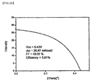
- a graph showing current-voltage characteristics of a solar cell using the thin film is illustrated in FIG. 26 .
- compositions of particles manufactured according to Examples 1 to 7 and Comparative Example 1 were analyzed. Results are summarized in Table 1 below. Photoelectric efficiencies of thin film solar cells, which are based on the above particles, manufactured according to Examples 12 to 16, and Comparative Example 3 were measured. Results are summarized in Table 2 below.
- J sc which is a variable determining the efficiency of each solar cell, represents current density
- V oc denotes an open circuit voltage measured at zero output current
- the photoelectric efficiency means a rate of cell output according to irradiance of light incident upon a solar cell plate
- fill factor (FF) represents a value obtained by dividing a value obtained by multiplication of current density and voltage values at a maximum power point by a value obtained by multiplication of Voc by J sc .
- the CI(G)S thin films manufactured using the aggregated precursor according to the present invention showed improvement in the current intensity, open circuit voltage, and photoelectric efficiency, when compared to CI(G)S thin films manufactured by using single-phase particles of the prior CuInS(Se) 2 .
- the current intensity and open circuit voltage of the CI(G)S thin films manufactured using the aggregated precursor according to the present invention were extremely superior
- the thin film when a thin film is manufactured using an aggregated precursor including a first phase including a copper (Cu)-containing chalcogenide and a second phase including an indium (In) and/or gallium (Ga)-containing chalcogenide according to the present invention manufactured in one reactor through a sequential process, the thin film has an entirely uniform composition and is stable against oxidization.
- the precursor includes S or Se and thereby the amount of a Group VI element in a final thin film is increased, and, accordingly, a superior quality thin film may be manufactured.
Landscapes
- Chemical & Material Sciences (AREA)
- Engineering & Computer Science (AREA)
- Life Sciences & Earth Sciences (AREA)
- Materials Engineering (AREA)
- Wood Science & Technology (AREA)
- Organic Chemistry (AREA)
- Photovoltaic Devices (AREA)
- Nanotechnology (AREA)
Abstract
Description
- The present invention relates to an aggregated precursor for manufacturing a light absorption layer of solar cells and a method of manufacturing the same.
- Recently, people are more concerned about environmental problems and depletion of natural resources and, as such, interest in solar cells as an alternative energy source which does not cause environmental pollution is growing. Solar cells are classified into silicon solar cells, thin film-type compound solar cells, layered-type solar cells and the like. Among these solar cells, silicon semiconductor solar cells have been studied the most widely.
- Among these solar cells, recently, thin film type compound solar cells are actively studied and developed.
- Among thin film type compound semiconductors, Cu(In1-xGax)(SeyS1-y) (CI(G)S), which is a Group I-III-VI compound included in ternary compounds, has a direct transition type energy band gap of 1 eV or more and high light absorption coefficient. In addition, the Cu(In1-xGax)(SeyS1-y) (CI(G)S) is an electro-optically stable. Thus, the Cu(In1-xGax)(SeyS1-y) (CI(G)S) is an ideal material as a light absorption layer of solar cells.
- CI(G)S based solar cells are made by forming a light absorption layer having a thickness of several microns. As methods of manufacturing the light absorption layer, a vacuum deposition method which does not require a precursor, a sputtering method which forms a CI(G)S thin film through heat treatment after forming a thin film with a precursor and an electrodeposition method were introduced. Recently, an ink coating method was introduced. According to the ink coating method, under non-vacuum, a precursor material is coated and then the coated material is heat-treated. Among these light absorption layer manufacturing methods, studies into the ink coating method are actively conducted since, by using the ink coating method, process costs may be reduced and a large area may be uniformly manufactured. Precursors used in the ink coating method may be various compounds or metals such as metal chalcogenide compounds, bimetallic metal particles, metal salts, metal oxides or the like.
- In particular, when a metal chalcogenide compound is used as a precursor, a mixed Cu-Se and In-Se compound or synthesized CuInSe2 single-phase particles are used. When the mixed particles are used, a coating layer having a partially non-uniform composition may be formed. When the CuInSe2 single-phase particles are used, long reaction time for particle growth is required.
- Therefore, there is a high need to develop a technology for a precursor which may form a highly efficient light absorption layer having an entirely more uniform composition, being stable against oxidation and having increased film density.
- Therefore, the present invention has been made to solve the above and other technical problems that have yet to be resolved.
- As a result of a variety of intensive studies and various experiments, the inventors of the present invention developed an aggregated precursor including a first phase including a copper (Cu)-containing chalcogenide and a second phase including an indium (In) and/or gallium (Ga)-containing chalcogenide such that all constituting elements forming a light absorption layer are included, and confirmed that, when a thin film is manufactured using the aggregated precursor, the thin film has an entirely uniform composition and is stable against oxidation and the amount of a Group VI element included in the thin film is increased due to S or Se included in the precursor, thus completing the present invention.
- In accordance with one aspect of the present invention, provided is a precursor for manufacturing a light absorption layer including a first phase including a copper (Cu)-containing chalcogenide and a second phase including an indium (In) and/or gallium (Ga)-containing chalcogenide as an aggregated precursor wherein 30% or more aggregated precursors based on the total weight of the precursors are divided into particle aggregates including first phases and/or second phases, or independent particles having first phases or second phases in an ink solvent for manufacturing the light absorption layer in an ink solvent for manufacturing the light absorption layer.
- The term "aggregated precursor", as used in the present invention means a precursor type in which independent particles are uniformly aggregated such that two or more phases are included. The term "particle aggregate" means a type of independent particle aggregated to a small amount in a smaller range than the aggregated precursor as a portion separated from the aggregated precursor. In addition, the term "independent particle" means a single particle.
- Therefore, the aggregated precursor, particle aggregate and independent particles have different concepts in the present invention.
- In a specific embodiment, the diameters of the independent particles on which all constitutions are based may be 1 nanometer to 100 nanometers, particularly 5 nanometers to 100 nanometers.
- In addition, the diameter of the particle aggregate in which independent particles is aggregated in a small amount and which broadly means all type of two or more particles aggregated in a small amount may be 2 nanometers to 200 nanometers in the broadest range. The diameter of the aggregated precursor from which the particle aggregate originates may be 10 nanometers to 500 nanometers, particularly 15 nanometers to 300 nanometers in a broader range than the particle aggregate.
- Meanwhile, the "chalcogenide" of the present invention means a Group VI element, for example, a material including sulfur(S) and/or selenium (Se). In a specific embodiment, the copper (Cu)-containing chalcogenide may be at least one selected from the group consisting of CuyS (0.5≤y≤2.0) and CuySe (0.5≤y≤2.0), and the indium (In) and/or gallium (Ga) chalcogenide may be at least one selected from the group consisting of (Inx(Ga)1-x)mSen (0≤x≤1 and 0.5≤n/m≤2.5) and (Inx(Ga)1-x)mSn (0≤x≤1 and 0.5≤n/m≤2.5).
- As described above, when the aggregated precursor includes two or more phase types, the composition ratio of the chalcogenide element may be 0.5 mol to 3 mol based on 1 mol of a mixture of copper (Cu), indium (In) and gallium (Ga), with respect to the total amount of the aggregated precursor,.
- Outside this range, when the composition ratio of the chalcogenide element is less than 0.5 mol, the Group VI element is not sufficiently provided and, as such, a film in which the Group VI element is partially deficient may be formed. On the contrary, when the composition ratio of the chalcogenide element exceeds 3 mol, the Group VI element is non-uniformly distributed in a thin film and, as such, a film may non-uniformly grow.
- In addition, a composition ratio of copper (Cu) may be 0.7 to 1.2 based on 1 mol of a mixture of In and Ga with respect to the total amount of the aggregated precursor.
- Outside this range, when the composition ratio of copper (Cu) exceeds 1.2 mol, the first phase including the copper (Cu)-containing chalcogenide exists in a relatively large amount and, as such, particles may easily grow but Cu impurities may be generated. On the contrary, when the composition ratio of copper (Cu) is less than 0.7 mol, the first phase including the copper (Cu)-containing chalcogenide is deficient and thereby the diameters of the particles are small and formation of a p-type CI(G)S thin film is not easy, and, accordingly, performances are poor.
- As described above, in the ink solvent for manufacturing the light absorption layer, a certain amount or more of the aggregated precursor according the present invention is divided into the particle aggregate including the first phase and/or second phase, or independent particles having a first phase or a second phase.
- As described above, when some particle aggregates separated from the aggregated precursor exist in a uniformly distributed state, the separated particle aggregates may be more uniformly distributed than the aggregated precursor. Therefore, when an ink is coated to manufacture a thin film, coating properties may be improved. In addition, when compared with an ink manufactured using nanoparticles including a first phase or nanoparticles including a second phase separately dispersed in a solvent, an ink manufactured using the aggregated precursor has a more uniform composition. Further, when compared with an ink manufactured using single-phase particles including all elements forming a light absorption layer, by using an ink manufactured using the aggregated precursors, a CI(G)S thin film may be smoothly grown.
- The above ink solvent for manufacturing the light absorption layer will be separately described later.
- Methods of manufacturing the aggregated precursor for manufacturing the light absorption layer may be broadly divided into two methods.
- As a first example, a method of manufacturing the aggregated precursor including sulfur(S) and/or selenium (Se) includes:
- (i) preparing a first solution including a reducing agent;
- (ii) preparing a second solution including a sulfur(S) and/or selenium (Se) compound, a third solution including indium (In) salt and/or gallium (Ga) salt and a fourth solution including a copper (Cu) salt;
- (iii) mixing the first solution and second solution to manufacture a mixture;
- (iv) mixing and reacting the third solution with the mixture of the mixing to synthesize indium (In) and/or gallium (Ga)-containing chalcogenide particles; and
- (v) mixing the fourth solution with the solution including the indium (In) and/or gallium (Ga)-containing chalcogenide particles of the mixing and reacting to synthesize a first phase including a copper (Cu)-containing chalcogenide and a second phase including an indium (In) and/or gallium (Ga)-containing chalcogenide to synthesize the aggregated precursor for manufacturing a light absorption layer.
- In addition, as a method of manufacturing an aggregated precursor including sulfur(S) and/or selenium (Se), to obtain a more sufficient Group VI element, a mixture is manufactured by mixing a fifth solution including a reducing agent and a sixth solution including a sulfur(S) and/or selenium (Se) compound, regardless of step (i) to step (iii), before step (v), and the mixture is mixed with the solution including indium (In) and/or gallium (Ga)-containing chalcogenide particles and the fourth solution of step (v) to manufacture an aggregated precursor.
- Regardless of manufacturing methods, the method of manufacturing the aggregated precursor according to the present invention is carried out through sequential processes in one reactor and, as such, the aggregated precursor has unique characteristics described above and may have a more uniform composition when compared with a precursor manufactured by separately synthesizing the nanoparticles including the first phase and the nanoparticles including the second phase, and then mixing the nanoparticles including the first phase or the nanoparticles including the second phase. As well as, when compared with use of CuInS(Se)2 single-phase particles, time required for growth and reaction of particles times may be shortened.
- Especially, when the mixture was mixed with the third solution in step (iv) and the solution including the indium (In) and/or gallium (Ga)-containing chalcogenide particles of step (iv) and the fourth solution are mixed, by stirring a solution while slowly adding the third solution and fourth solution dropwise, an aggregated precursor having a uniform composition and size may be obtained.
- As a specific embodiment, in both cases, to improve dispersibility of an aggregated precursor and to obtain uniform composition distribution, when the fourth solution is mixed with the solution including the indium (In) and/or gallium (Ga)-containing chalcogenide particles of step (v), or a mixture of the fifth solution and the sixth solution, the solution including the indium (In) and/or gallium (Ga)-containing chalcogenide particles, and the fourth solution are mixed, an additive may be further added.
- The additive is not specifically limited so long as the additive may used as a dispersing agent and, for example, may be at least one selected from the group consisting of polyvinylpyrrolidone (PVP), polyvinyl alcohol, and ethyl cellulose.
- In a specific embodiment, the reducing agent included in the first solution may be an organic reducing agent and/or an inorganic reducing agent and particularly one selected from the group consisting of LiBH4, NaBH4, KBH4, Ca(BH4)2, Mg(BH4)2, LiB(Et)3H, NaBH3(CN), NaBH(OAc)3, hydrazine, ascorbic acid and triethanolamine.
- Accordingly, the method of manufacturing the aggregated precursor is performed by a solution process instead of the prior vacuum process and, as such, process costs may be reduced.
- In a specific embodiment, solvents for the first solution to sixth solution each independently may be at least one selected from the group consisting of water, alcohols, acetic acids, diethylene glycol (DEG), oleylamine, ethylene glycol, triethylene glycol, dimethyl sulfoxide, dimethyl formamide, and N-methyl-2-pyrrolidone (NMP). The alcohol solvents may be methanol, ethanol, propanol, butanol, pentanol, hexanol, heptanol and octanol having 1 to 8 carbons.
- In a specific embodiment, as the Group VI source included in the second solution, the sulfur (S) compound may be at least one selected from the group consisting of, for example, sulfur (S) powder, H2S, Na2S, K2S, CaS, (CH3)2S, H2SO4, and hydrates thereof, thiourea, and thioacetamide, and the selenium (Se) compound may be at least one selected from the group consisting of, for example, Se powder, H2Se, Na2Se, K2Se, CaSe, (CH3)2Se, SeO2, SeCl4, H2SeO3, H2SeO4 and hydrates thereof, selenourea, and selenous acid.
- In a specific embodiment, the salts included in the third solution and fourth solution may be at least one selected from the group consisting of chlorides, bromides, iodides, nitrates, nitrites, sulfates, acetates, sulfites, acetylacetonate and hydroxides.
- Meanwhile, as another example, a method of manufacturing the aggregated precursor including sulfur(S) and/or selenium (Se) includes:
- (i) preparing a first solution including a sulfur (S) and/or selenium (Se) compound, a second solution including an indium (In) salt or indium (In) salt and gallium (Ga) salt, and a third solution including a copper (Cu) salt;
- (ii) mixing and reacting the first solution and second solution to synthesize indium (In) and/or gallium (Ga)-containing chalcogenide particles; and
- (iii) mixing the third solution with the solution including the indium (In) and/or gallium (Ga)-containing chalcogenide particles of step (ii) to synthesize and purify an aggregated precursor for manufacturing a light absorption layer including the first phase including the copper (Cu)-containing chalcogenide and the second phase including the indium (In) and/or gallium (Ga)-containing chalcogenide.
- Accordingly, the method of manufacturing the aggregated precursor is carried out by a solution process instead of a vacuum process and, as such, process costs may be reduced.
- The second method of manufacturing the aggregated precursor is similar to the first method of manufacturing the aggregated precursor in that, to obtain a sufficient amount of the Group VI element, when the third solution is mixed with the solution including the indium (In) and/or gallium (Ga)-containing chalcogenide particles of step (iii), an aggregated precursor may be manufactured by mixing the fourth solution including the sulfur (S) and/or selenium (Se) compound besides the first solution of step (i).
- Regardless of manufacturing methods, the method of manufacturing the aggregated precursor according to the present invention is carried out through sequential processes in one reactor and, as such, the aggregated precursor has unique characteristics described above and may have a more uniform composition when compared with a precursor manufactured by separately synthesizing the nanoparticles including the first phase and nanoparticles including the second phase, and then mixing the nanoparticles including the first phase or the nanoparticles including the second phase. In addition, when compared with use of CuInS(Se)2 single-phase particles, time required for growth and reaction of particles times may be shortened
- In addition, when the first solution and second solution are mixed, and the third solution is mixed with the solution including the indium (In) and/or gallium (Ga)-containing chalcogenide particles of step (ii), by stirring a mixture while slowly adding the second solution and third solution dropwise, an aggregated precursor having a uniform composition and size may be obtained.
- As a specific embodiment, in both cases, to improve dispersibility of an aggregated precursor and to obtain uniform composition distribution, when the third solution is mixed with the solution including the indium (In) and/or gallium (Ga)-containing chalcogenide particles of step (iii), or the solution including the indium (In) and/or gallium (Ga)-containing chalcogenide particles, the third solution and the fourth solution are mixed, and an additive may be further added.
- Here, concrete examples of the additive are the same as those described above.
- In addition, the other solvent and salt types of the sulfur (S) compound, selenium (Se) compound and the first solution to fourth solution are the same as those described above.
- The present invention also provides a method of manufacturing a thin film using the ink composition.
- A method of manufacturing the thin film according to the present invention includes:
- (i) dispersing an aggregated precursor for manufacturing a light absorption layer including a first phase including a copper (Cu)-containing chalcogenide and a second phase including an indium (In) and/or gallium (Ga)-containing chalcogenide in a solvent to manufacture an ink;
- (ii) coating the ink on a base provided with an electrode; and
- (iii) drying and then heat-treating the ink coated on the base provided with an electrode.
- As a specific embodiment, the solvent of step (i) is not particularly limited so long as the solvent is a general organic solvent and may be one organic solvent selected from among alkanes, alkenes, alkynes, aromatics, ketones, nitriles, ethers, esters, organic halides, alcohols, amines, thiols, carboxylic acids, phosphines, phosphites, phosphates, sulfoxides, and amides or a mixture of at least one organic solvent selected therefrom.
- In particular, the alcohols may be at least one mixed solvent selected from among ethanol, 1-propanol, 2-propanol, 1-pentanol, 2-pentanol, 1-hexanol, 2-hexanol, 3-hexanol, heptanol, octanol, ethylene glycol (EG), diethylene glycol monoethyl ether (DEGMEE), ethylene glycol monomethyl ether (EGMME), ethylene glycol monoethyl ether (EGMEE), ethylene glycol dimethyl ether (EGDME), ethylene glycol diethyl ether (EGDEE), ethylene glycol monopropyl ether (EGMPE), ethylene glycol monobutyl ether (EGMBE), 2-methyl-1-propanol, cyclopentanol, cyclohexanol, propylene glycol propyl ether (PGPE), diethylene glycol dimethyl ether (DEGDME), 1,2-propanediol (1,2-PD), 1,3-propanediol (1,3-PD), 1,4-butanediol (1,4-BD), 1,3-butanediol (1,3-BD), α-terpineol, diethylene glycol (DEG), glycerol, 2-(ethylamino)ethanol, 2-(methylamino)ethanol, and 2-amino-2-methyl-1-propanol.
- The amines may be at least one mixed solvent selected from among triethyl amine, dibutyl amine, dipropyl amine, butylamine, ethanolamine, diethylenetriamine (DETA), triethylenetetramine (TETA), triethanolamine, 2-aminoethyl piperazine, 2-hydroxyethyl piperazine, dibutylamine, and tris(2-aminoethyl)amine.
- The thiols may be at least one mixed solvent selected from among 1,2-ethanedithiol, pentanethiol, hexanethiol, and mercaptoethanol.
- The alkanes may be at least one mixed solvent selected from among hexane, heptane, and octane.
- The aromatics may be at least one mixed solvent selected from among toluene, xylene, nitrobenzene, and pyridine.
- The organic halides may be at least one mixed solvent selected from among chloroform, methylene chloride, tetrachloromethane, dichloroethane, and chlorobenzene.
- The nitriles may be acetonitrile.
- The ketones may be at least one mixed solvent selected from among acetone, cyclohexanone, cyclopentanone, and acetyl acetone.
- The ethers may be at least one mixed solvent selected from among ethyl ether, tetrahydrofuran, and 1,4-dioxane.
- The sulfoxides may be at least one mixed solvent selected from among dimethyl sulfoxide (DMSO) and sulfolane.
- The amides may be at least one mixed solvent selected from among dimethyl formamide (DMF) and n-methyl-2-pyrrolidone (NMP).
- The esters may be at least one mixed solvent selected from among ethyl lactate, γ-butyrolactone, and ethyl acetoacetate.
- The carboxylic acids may be at least one mixed solvent selected from among propionic acid, hexanoic acid, meso-2,3-dimercaptosuccinic acid, thiolactic acid, and thioglycolic acid.
- However, the solvents are only given as an example, and embodiments of the present invention are not limited thereto.
- In some cases, the ink of step (i) may further include an additive.
- The additive may, for example, be at least one selected from the group consisting of a dispersant, a surfactant, a polymer, a binder, a crosslinking agent, an emulsifying agent, an anti-foaming agent, a drying agent, a filler, a bulking agent, a thickening agent, a film conditioning agent, an antioxidant, a fluidizer, a leveling agent, and a corrosion inhibitor. In particular, the additive may be at least one selected from the group consisting of polyvinylpyrrolidone (PVP), polyvinyl alcohol, Anti-terra 204, Anti-terra 205, ethyl cellulose, and DispersBYK110.
- The coating of step (ii) may be any one selected from the group consisting of wet coating, spray coating, spin-coating, doctor blade coating, contact printing, top feed reverse printing, bottom feed reverse printing, nozzle feed reverse printing, gravure printing, micro gravure printing, reverse micro gravure printing, roller coating, slot die coating, capillary coating, inkjet-printing, jet deposition, and spray deposition.
- The heat treatment of step (iii) may be carried out at a temperature of 400 to 900 □.
- Meanwhile, a selenization process may be included to prepare the thin film of a solar cell having much higher density. The selenization process may be carried out through a variety of methods.
- As a first example, effects obtained from the selenization process may be achieved by manufacturing an ink by dispersing S and/or Se in a particle type in a solvent with the aggregated precursor for manufacturing the light absorption layer in step (i), and by combining the heat treatment of step (iii)
- As a second example, effects obtained from the selenization process may be achieved through the heat treatment of step (iii) in the presence of S or Se
- In particular, S or Se may be present by supplying H2S or H2Se in a gaseous state or supplying Se or S in a gaseous state through heating.
- As a third example, after step (ii), S or Se may be stacked on the coated base, followed by performing step (iii). In particular, the stacking process may be performed by a solution process or a deposition method.
- The present invention also provides a thin film manufactured according to the above method.
- The thickness of the thin film may be 0.5 to 5.0 µm, more particularly 0.5 to 3.0 µm.
- When the thickness of the thin film is less than 0.5 µm, the density and amount of the light absorption layer are insufficient and thus desired photoelectric efficiency may not be obtained. On the other hand, when the thickness of the thin film exceeds 5.0 µm, movement distances of carriers increases and, accordingly, there is an increasing probability of recombination, which results in reduced efficiency.
- Furthermore, the present invention provides a thin film solar cell manufactured using the thin film.
- A method of manufacturing a thin film solar cell is known in the art and thus a detailed description thereof will be omitted herein.
- The above and other objects, features and other advantages of the present invention will be more clearly understood from the following detailed description taken in conjunction with the accompanying drawing, in which:
-
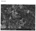
FIG. 1 is a scanning electron microscope (SEM) image of In2Se3-CuSe powder formed according to Example 1; -
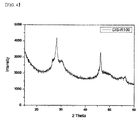
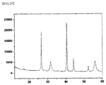
FIG. 2 is an X-ray diffraction (XRD) graph of In2Se3-CuSe powder formed according to Example 1; -
FIG. 3 is a scanning electron microscope (SEM) image of In2Se3-CuSe powder formed according to Example 2; -
FIG. 4 is an X-ray diffraction (XRD) graph of In2Se3-CuSe powder formed according to Example 2; -
FIG. 5 is a scanning electron microscope (SEM) image of In2Se3-CuSe powder formed according to Example 3; -
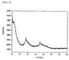
FIG. 6 is an X-ray diffraction (XRD) graph of In2Se3-CuSe powder formed according to Example 3; -
FIG. 7 is a scanning electron microscope (SEM) image of In0.7Ga0.3Se1.5-CuSe powder formed according to Example 4; -
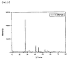
FIG. 8 is an X-ray diffraction (XRD) graph of In0.7Ga0.3Se1.5-CuSe powder formed according to Example 4; -
FIG. 9 is a scanning electron microscope (SEM) image of In2S3-Cusulfur (S) powder formed according to Example 5; -
FIG. 10 is a scanning electron microscope (SEM) image of (In,Ga)2Se3-CuSe powder formed according to Example 6; -
FIG. 11 is an X-ray diffraction (XRD) graph of (In,Ga)2Se3-CuSe powder formed according to Example 6; -
FIG. 12 is a scanning electron microscope (SEM) image of In2Se3-CuSe powder formed according to Example 7; -
FIG. 13 is an X-ray diffraction (XRD) graph of In2Se3-CuSe powder formed according to Example 7; -
FIG. 14 is a scanning electron microscope (SEM) image of CuInSe2 powder formed according to Comparative Example 1; -
FIG. 15 is an XRD graph of CuInSe2 powder formed according to Comparative Example 1; -
FIG. 16 is an SEM image of a thin film manufactured according to Example 8; -
FIG. 17 is an XRD graph of a thin film manufactured according to Example 8; -
FIG. 18 is an SEM image of a thin film manufactured according to Example 9; -
FIG. 19 is an XRD graph of a thin film manufactured according to Example 9; -
FIG. 20 is an SEM image of a thin film manufactured according to Example 10; -
FIG. 21 is an XRD graph of a thin film manufactured according to Example 10; -
FIG. 22 is an SEM image of a thin film manufactured according to Example 11; -
FIG. 23 is an XRD graph of a thin film manufactured according to Example 11; -
FIG. 24 is an SEM image of a thin film manufactured according to Comparative Example 2; -
FIG. 25 is an XRD graph of a thin film manufactured according to Comparative Example 2; and -
FIG. 26 is a graph showing IV characteristics of a thin film solar cell manufactured according to Example 15. - Now, the present invention will be described in more detail with reference to the following examples. These examples are provided only for illustration of the present invention and should not be construed as limiting the scope and spirit of the present invention.
- Under a nitrogen atmosphere, after mixing 1.974 g of NaBH4 in 100 ml of distilled water, 1.974 g of Se powder was added thereto and then 100 ml of distilled water was further added. After confirming formation of a colorless and transparent solution, the solution was further stirred for 15 minutes. Subsequently, a solution produced by dissolving 2.212 g of InCl3 in 50 ml distilled water was added thereto. The resulting mixture was further stirred for 10 minutes and then 50 ml of distilled water in which 1.705 g of CuCl2 was dissolved was slowly added thereto. The resulting mixture was further stirred for 1 hour and then centrifuged. As a result, powder having a CuInSe2.5 composition was obtained in a yield of 99%. The powder was analyzed using ICP. As a result, it was confirmed that the CuInSe2.5 composition of the powder has a ratio of Cu:In:Se of 22.18:22.56:55.26 in mol%. As an XRD analysis result of the particles, CuSe crystalline phases were observed and it was confirmed that amorphous In2Se3 and superior CuSe crystalline phases were mixed. SEM-EDX and XRD analysis results of the particles are illustrated in
FIGS. 1 and2 . - Under a nitrogen atmosphere, after mixing 1.90 g of NaBH4 in 150 ml of distilled water, 3.224 g of H2SeO3 dissolved in 60 ml of distilled water was added dropwise. After confirming formation of a colorless and transparent solution, a solution produced by dissolving 2.212 g of InCl3 in 35 ml of distilled water was added thereto and then stirred for 5 minutes. Subsequently, 40 ml of distilled water in which 1.705 g of CuCl2*2H2O was dissolved was added thereto. The resulting mixture was further stirred for one day and then centrifuged. As a result, powder having a CuInSe2.5 composition was obtained in a yield of 99%. The powder was analyzed using ICP. As a result, it was confirmed that the CuInSe2.5 composition of the powder has a ratio of Cu: In: Se of 2.42: 22.20: 56.38 in mol%. As an XRD analysis result of the particles, CuSe crystalline phases were observed and it was confirmed that amorphous In2Se3 and superior CuSe crystalline phases were mixed. SEM-EDX and XRD analysis results of the particles are illustrated in
FIGS. 3 and4 . - Under a nitrogen atmosphere, 1.135 g of NaBH4 was added to 50 ml of distilled water and dissolved therein. Subsequently, a solution produced by dissolving 1.935 g of H2SeO3 in 30 ml of distilled water was added thereto. After confirming formation of a colorless and transparent solution, a solution produced by dissolving 2.212 g of InCl3 in 50 ml of distilled water was added thereto and then was further stirred for 3.5 hours, resulting in In2Se3 particle formation. Under a nitrogen atmosphere, after dissolving 0.757 g of NaBH4 in 50 ml of distilled water in another flask and then a solution produced by dissolving 1.290 g of H2SeO3 in 20 ml of distilled water was added thereto. The resulting mixture was stirred until a clear solution was observed. To this clear solution, the previously manufactured In2Se3 solution was added. Subsequently, a solution produced by dissolving 1.705 g of CuCl2*2H2O in 50 ml of distilled water was added thereto and then was stirred for 1 day. The resulting solution was purified through centrifugation and then vacuum-dried, resulting in particles having a CuInSe2.5 composition. The particles were analyzed using ICP. As a result, it was confirmed that the CuInSe2.5 composition particles have a composition as follows: Cu:In:Se of 21.80:21.89:56.31 in mol%. In addition, as an XRD analysis result, the particles were observed as having a CuSe crystalline phase and as being in a mixed state of amorphous In2Se3 and CuSe having superior crystallinity. SEM-EDX and XRD results of the particles are illustrated in
FIGS. 5 and6 . - Under a nitrogen atmosphere, 2.270 g of NaBH4 was added to 100 ml of distilled water and dissolved therein. Subsequently, a solution produced by dissolving 3.869 g of H2SeO3 in 60 ml of distilled water was added thereto. After confirming formation of a colorless and transparent solution, a solution produced by dissolving 3.097 g of InCl3 and 2.703 g of GaI3 in 100 ml of distilled water was added thereto and then was further stirred for 1 day, resulting in In0.7Ga0.3Se1.5 particle formation. Under a nitrogen atmosphere, after dissolving 1.665 g of NaBH4 in 100 ml of distilled water in another flask and then a solution produced by dissolving 2.837 g of H2SeO3 in 40 ml of distilled water was added thereto. The resulting mixture was stirred until a clear solution was observed. To this clear solution, the previously manufactured In0.7Ga0.3Se1.5 solution was added. Subsequently, a solution produced by dissolving 3.410 g of CuCl2*2H2O in 100 ml of distilled water was added thereto and then was stirred for five hours. The resulting solution was purified through centrifugation and then vacuum-dried, resulting in particles having a CuIn0.7Ga0.3Se2.5 composition. The particles were analyzed using ICP. As a result, it was confirmed that the CuIn0.7Ga0.3Se2.5 composition particles have a composition as follows: Cu:In:Ga:Se:Na:B of 20.07: 14.19:5.88:55.885:3.73:0.26 in mol%. In addition, as an XRD analysis result, the particles were observed as having a CuSe crystalline phase and as being in a mix state of amorphous (In,Ga)2Se3 and CuSe having superior crystallinity. SEM-EDX and XRD results of the particles are illustrated in
FIGS. 7 and8 . - Under a nitrogen atmosphere, 3.603 g of Na2S*9H2O was dissolved in 60 ml of distilled water and then a solution produced by dissolving 2.212 g of InCl3 in 40 ml of distilled water was added thereto. The resulting solution was further stirred for one hour. To the solution, a solution produced by dissolving 2.402 g of Na2S*9H2O in 50 ml of distilled water was added and then stirred for ten minutes. Subsequently, a solution produced by dissolving 1.705 g of CuCl2*2H2O in 50 ml of distilled water was added thereto and then was further stirred for three hours. The resulting solution was purified through centrifugation and then vacuum-dried. As a result, particles including Cu and In in a ratio as follows: Cu:In of 2.64:3.10 were obtained. SEM-EDX results of the particles are illustrated in
FIG. 9 . - Under a nitrogen atmosphere, 1.135 g of NaBH4 was added to 50 ml of distilled water and dissolved therein. Subsequently, a solution produced by dissolving 1.935 g of H2SeO3 in 30 ml of distilled water was added thereto. After confirming formation of a colorless and transparent solution, a solution produced by dissolving 1.548 g of InCl3 and 1.351 g of GaI3 in 50 ml of distilled water was added thereto and then was further stirred for 1 day, resulting in In0.7Ga0.3Se1.5 particle formation. Under a nitrogen atmosphere, after dissolving 0.666 g of NaBH4 in 50 ml of distilled water in another flask and then a solution produced by dissolving 1.135 g of H2SeO3 in 20 ml of distilled water was added thereto. The resulting mixture was stirred until a clear solution was observed. To this clear solution, the previously manufactured (In,Ga)2Se3 solution was added. Subsequently, a solution produced by dissolving 1.364 g of CuCl2*2H2O in 50 ml of distilled water was added thereto and then was stirred for six hours. The resulting solution was purified through centrifugation and then vacuum-dried, resulting in particles having a Cu0.81In0.74Ga0.26Se2.5 composition. The particles were analyzed using ICP. As a result, it was confirmed that the Cu0.8In0.74Ga0.26Se2.5 composition particles have a composition as follows: Cu:In:Ga:Se:Na:B of 17.62:16.18:5.61: 56.22:4.16:0.22 in mol%. In addition, as an XRD analysis result, the particles were observed as having a CuSe crystalline phase and as being in a mix state of amorphous (In,Ga)2Se3 and CuSe having superior crystallinity. SEM-EDX and XRD results of the particles are illustrated in
FIGS. 10 and11 . - Under a nitrogen atmosphere, 1.248 g of NaBH4 was added to 50 ml of distilled water and dissolved therein. Subsequently, a solution produced by dissolving 2.128 g of H2SeO3 in 30 ml of distilled water was added thereto. After confirming formation of a colorless and transparent solution, a solution produced by dissolving 2.212 g of InCl3 in 50 ml of distilled water was added thereto and then was further stirred for 1 day, resulting in In2Se3 particle formation. Under a nitrogen atmosphere, after dissolving 0.832 g of NaBH4 in 50 ml of distilled water in another flask and then a solution produced by dissolving 1.419 g of H2SeO3 in 20 ml of distilled water was added thereto. The resulting mixture was stirred until a clear solution was observed. To this clear solution, the previously manufactured In2Se3 solution was added. Subsequently, a solution produced by dissolving 1.705 g of CuCl2*2H2O in 50 ml of distilled water and a solution produced by dissolving 0.111 g of polyvinylpyrrolidone in 20 ml of distilled water were added thereto and then was stirred for five hours. The resulting solution was purified through centrifugation and then vacuum-dried, resulting in particles having a CuInSe2.5 composition. The particles were analyzed using ICP. As a result, it was confirmed that the CuInSe2.5 composition particles have a composition as follows: Cu:In:Se:Na:B of 19.49:19.97:48.81:3.75:7.98 in mol%. In addition, as an XRD analysis result, the particles were observed as having a CuSe crystalline phase and as being in a mix state of amorphous In2Se3 and CuSe having superior crystallinity. SEM-EDX and XRD results of the particles are illustrated in
FIGS. 12 and13 . - 8 mmol of CuCl, 10 mmol of InCl3 and 20 mmol of Se powder were added to 100 ml of oleylamine and then were stirred for four hours while heating to 80 °C under vacuum suction. Subsequently, the resulting mixture was reacted for four hours at 240 °C under a nitrogen atmosphere and then was cooled off. The resulting reactant was purified through centrifugation using hexane and ethanol. As a result, nanoparticles having a CuInSe2 composition were obtained. SEM-EDX and XRD results of the particles are illustrated in
FIGS. 14 and15 . - Particles having a CuIn0.7Ga0.3Se2.5 composition manufactured according to Example 4 were added to a mix solvent including ethanol, ethylene glycol monomethyl ether, acetylacetone, propylene glycol proyl ether, cyclohexanone, ethanolamine, 1,2-propanediol, diethylene glycol monoethyl ether, glycerol and sodium dodecyl sulfate, and then were dispersed in a concentration of 21% to manufacture an ink. The obtained ink was coated on glass coated wiht a Mo thin film and then dried up to 200 °C. The coated glass was heat-treated at 550 °C under a Se-containing atmosphere, resulting in a CIGS thin film. SEM-EDX and XRD results of the resulting thin film are illustrated in
FIGS. 16 and17 . - The particles having a CuIn0.7Ga0.3Se2.5 composition manufactured according to Example 4 and CuSe particles were mixed in a ratio of 24% and 1.2%. The resulting mixture was added to a mix solvent including ethylene glycol monomethyl ether, propylene glycol proyl ether, ethanolamine, 1,2-propanediol and diethylene glycol monoethyl ether, and then dispersed to manufacture an ink. The obtained ink was coated on glass coated with a Mo thin film and then dried up to 200 □. The coated glass was heat-treated at 550 □ under a Se-containing atmosphere, resulting in a CIGS thin film. SEM-EDX and XRD results of the resulting thin film are illustrated in
FIGS. 18 and19 . - The particles having a Cu0.8In0.7G0.3Se2.5 composition manufactured according to Example 6 and Cu0.87Se nanoparticles were mixed. The resulting mixture was added to a mix solvent including ethylene glycol monomethyl ether, propylene glycol proyl ether, ethanolamine, 1,2-propanediol and diethylene glycol monoethyl ether, and then dispersed to manufacture an ink. The obtained ink was coated on glass coated wih a Mo thin film and then dried up to 200 °C. The coated glass was heat-treated at 550 °C under a Se-containing atmosphere, resulting in a CIGS thin film. SEM-EDX and XRD results of the resulting thin film are illustrated in
FIGS. 20 and21 . - Particles having a CuInSe2.5 composition manufactured according to Example 7 were added to a mix solvent including ethanol, ethylene glycol monomethyl ether, acetylacetone, propylene glycol proyl ether and cyclohexanone, and then were dispersed in a concentration of 20% to manufacture an ink. The obtained ink was coated on glass coated with Mo thin film and then dried up to 160 □. The coated glass was pressed with a pressure of 300 bar and then heat-treated at 550□ under a Se-containing atmosphere, resulting in a CIS thin film. SEM-EDX and XRD results of the resulting thin film are illustrated in
FIGS. 22 and23 . - Particles having a CuInSe2 composition manufactured according to Comparative Example 1 were added to a mix solvent including ethanol, ethylene glycol monomethyl ether, acetylacetone, propylene glycol proyl ether, cyclohexanone and then dispersed in a concentration of 20% to manufacture an ink. The obtained ink was coated on glass coated with a Mo thin film and then dried up to 160°C. Subsequently, the coated class was pressed at a pressure of 300 bar and then heat-treated at 550 °C under a Se-containing atmosphere, resulting a CIS thin film. SEM-EDX and XRD results of the resulting thin film are illustrated in
FIGS. 24 and25 . As shown inFIG. 24 , it was confirmed that the thin film manufactured using the CuInSe2 particles had lots of voids and particle growth was slow. - A CdS buffer layer was manufactured on a CIGS thin film manufactured according to Example 8 using a CBD method. Subsequently, ZnO and Al:ZnO were sequentially deposited on the CIGS thin film by sputtering and then an A1 electrode was deposited on the deposited CIGS thin film by e-beam to manufacture a cell. The resulting cell showed characteristics as follows: Jsc=24.86 mA/sqcm, Voc=0.23 V, FF=36.55%, and Eff=2.09 %.
- A CdS buffer layer was manufactured on a CIGS thin film manufactured according to Example 9 using a CBD method. Subsequently, ZnO and Al:ZnO were sequentially deposited on the CIGS thin film by sputtering and then an Al electrode was deposited on the deposited CIGS thin film by e-beam to manufacture a cell. The resulting cell showed characteristics as follows: Jsc=29.33 mA/sqcm, Voc=0.42 V, FF= 42.0% and Eff= 5.20 %.
- A CdS buffer layer was manufactured on a CIGS thin film manufactured according to Example 9 using a CBD method. Subsequently, ZnO and Al:ZnO were sequentially deposited on the CIGS thin film by sputtering and then an Ag electrode was deposited on the deposited CIGS thin film by screen-printing to manufacture a cell. The resulting cell showed characteristics as follows: Jsc=34.07 mA/sqcm, Voc=0.30 V, FF=34.28% and Eff= 3.48%.
- A CdS buffer layer was manufactured on a CIGS thin film manufactured according to Example 10 using a CBD method. Subsequently, ZnO and Al:ZnO were sequentially deposited on the CIGS thin film by sputtering and then an Al electrode was deposited on the deposited CIGS thin film by e-beam to manufacture a cell. The resulting cell showed characteristics as follows: Jsc=26.87 mA/sqcm, Voc=0.43 V, FF=49.01% and Eff= 5.61%. A graph showing current-voltage characteristics of a solar cell using the thin film is illustrated in
FIG. 26 . - A CdS buffer layer was manufactured on a CIS thin film manufactured according to Example 11 using a CBD method. Subsequently, ZnO and Al:ZnO were sequentially deposited on the CIS thin film by sputtering and then an Al electrode was deposited on the deposited CIS thin film by e-beam to manufacture a cell. The resulting cell showed characteristics as follows: Jsc=28.37 mA/sqcm, Voc = 0.23 V, FF = 34.08% andEff=2.19%.
- A CdS buffer layer was manufactured on a CIS thin film manufactured according to Comparative Example 2 using a CBD method. Subsequently, ZnO and Al:ZnO were sequentially deposited on the CIS thin film by sputtering and then an Al electrode was deposited on the deposited CIS thin film by e-beam to manufacture a cell. The resulting cell showed characteristics as follows: Jsc=13.45 mA/sqcm, Voc = 0.18 V, FF = 26.63% and Eff= 0.6 %.
- Compositions of particles manufactured according to Examples 1 to 7 and Comparative Example 1 were analyzed. Results are summarized in Table 1 below. Photoelectric efficiencies of thin film solar cells, which are based on the above particles, manufactured according to Examples 12 to 16, and Comparative Example 3 were measured. Results are summarized in Table 2 below.
[Table 1] Cu Se or S In Ga atomic% atomic% atomic% atomic% Example 1 23.9 52.85 23.26 - Example 2 24.86 55.21 19.94 - Example 3 27.17 51.9 20.93 - Example 4 25.67 51.77 13.86 8.7 Example 5 28.48 49.86 21.66 - Example 6 22.45 57.05 13.22 7.29 Example 7 25.08 47.63 27.28 - Comparative Example 1 24.83 51.82 23.35 [Table 2] Jsc (mA/cm2) Voc (V) FF (%) Photoelectric efficiency (%) Example 12 24.86 0.23 36.55 2.09 Example 13 29.33 0.42 42.0 5.20 Example 14 34.07 0.30 34.28 3.48 Example 15 26.87 0.43 49.01 5.61 Example 16 28.37 0.23 34.08 2.19 Comparative Example 3 13.45 0.18 26.63 0.6 - In Table 2, Jsc, which is a variable determining the efficiency of each solar cell, represents current density, Voc denotes an open circuit voltage measured at zero output current, the photoelectric efficiency means a rate of cell output according to irradiance of light incident upon a solar cell plate, and fill factor (FF) represents a value obtained by dividing a value obtained by multiplication of current density and voltage values at a maximum power point by a value obtained by multiplication of Voc by Jsc.
- Referring to Table 2 and
FIG. 26 , the CI(G)S thin films manufactured using the aggregated precursor according to the present invention showed improvement in the current intensity, open circuit voltage, and photoelectric efficiency, when compared to CI(G)S thin films manufactured by using single-phase particles of the prior CuInS(Se)2. Especially, the current intensity and open circuit voltage of the CI(G)S thin films manufactured using the aggregated precursor according to the present invention were extremely superior - Those skilled in the art will appreciate that various modifications, additions and substitutions are possible, without departing from the scope and spirit of the invention as disclosed in the accompanying claims.
- As described above, when a thin film is manufactured using an aggregated precursor including a first phase including a copper (Cu)-containing chalcogenide and a second phase including an indium (In) and/or gallium (Ga)-containing chalcogenide according to the present invention manufactured in one reactor through a sequential process, the thin film has an entirely uniform composition and is stable against oxidization. In addition, the precursor includes S or Se and thereby the amount of a Group VI element in a final thin film is increased, and, accordingly, a superior quality thin film may be manufactured.
Claims (31)
- An aggregated precursor for manufacturing a light absorption layer of solar cells comprising a first phase comprising a copper (Cu)-containing chalcogenide and a second phase comprising an indium (In) and/or gallium (Ga)-containing chalcogenide wherein 30% or more aggregated precursors based on a total weight of precursors are divided into particle aggregates comprising first phases and/or second phases, or independent particles having first phases or second phases.
- The aggregated precursor according to claim 1, wherein the aggregated precursor has a diameter of 10 nanometers to 500 nanometers.
- The aggregated precursor according to claim 1, wherein the particle aggregate has a diameter of 2 nanometers to 200 nanometers.
- The aggregated precursor according to claim 1, wherein the independent particles have diameters of 1 nanometer to 100 nanometers.
- The aggregated precursor according to claim 1, wherein the copper (Cu)-containing chalcogenide is at least one selected from the group consisting of CuyS wherein 0.5≤y≤2.0 and CuySe wherein 0.5≤y≤2.0.
- The aggregated precursor according to claim 1, wherein the indium (In) and/or gallium (Ga)-containing chalcogenide is at least one selected from the group consisting of (Inx(Ga)1-x)mSen wherein 0≤x≤1 and 0.5≤n/m≤2.5, and (Inx(Ga)1-x)mSn wherein 0≤x≤1 and 0.5≤n/m≤2.5.
- The aggregated precursor according to claim 1, wherein composition ratios of chalcogenide elements present in the aggregated precursor are 0.5 mol to 3 mol based on 1 mol of a mixture comprising copper (Cu), indium (In) and gallium (Ga).
- The aggregated precursor according to claim 1, wherein a composition ratio of the copper (Cu) present in the aggregated precursor is 0.7 to 1.2 mol based on 1 mol of a mixture of In and Ga.
- A method of manufacturing the aggregated precursor for manufacturing the light absorption layer according to claim 1, the method comprising:preparing a first solution comprising a reducing agent;preparing a second solution comprising a sulfur(S) and/or selenium (Se) compound, a third solution comprising indium (In) salt or indium (In) salt and gallium (Ga) salt and a fourth solution comprising a copper (Cu) salt;mixing the first solution and second solution to manufacture a mixture;mixing and reacting the third solution with the mixture of the mixing to synthesize indium (In) and/or gallium (Ga)-containing chalcogenide particles; andsynthesizing the aggregated precursor for manufacturing a light absorption layer by mixing the fourth solution with the solution comprising the indium (In) and/or gallium (Ga)-containing chalcogenide particles of the mixing and reacting to synthesize a first phase comprising a copper (Cu)-containing chalcogenide and a second phase comprising an indium (In) and/or gallium (Ga)-containing chalcogenide.
- The method according to claim 9, wherein, when the fourth solution is mixed with the indium (In) and/or gallium (Ga)-containing chalcogenide particles of the synthesizing, an additive is further added.
- The method according to claim 9, wherein, before the synthesizing, a fifth solution comprising a reducing agent and a sixth solution comprising a sulfur(S) and/or selenium (Se) compound are mixed to manufacture a mixture and then the mixture is mixed with the solution comprising the indium (In) and/or gallium (Ga)-containing chalcogenide particles of the synthesizing and the fourth solution, regardless of the preparing to the mixing.
- The method according to claim 11, wherein, when the mixture of the fifth solution and the sixth solution, the solution comprising indium (In) and/or gallium (Ga)-containing chalcogenide particles and the fourth solution are mixed, an additive is further added.
- The method according to claim 9 or 11, wherein the reducing agent is an organic reducing agent and/or inorganic reducing agent.
- The method according to claim 13, wherein the reducing agent is one selected from the group consisting of LiBH4, NaBH4, KBH4, Ca(BH4)2, Mg(BH4)2, LiB(Et)3H2, NaBH3(CN), NaBH(OAc)3, hydrazine, ascorbic acid and triethanolamine.
- A method of manufacturing the aggregated precursor for manufacturing the light absorption layer according to claim 1, the method comprising:preparing a first solution comprising a sulfur (S) and/or selenium (Se) compound, a second solution comprising an indium (In) salt or indium (In) salt and gallium (Ga) salt, and a third solution comprising a copper (Cu) salt;mixing and reacting the first solution and the second solution to synthesize indium (In) and/or gallium (Ga)-containing chalcogenide particles; andmixing the third solution with the solution comprising the indium (In) and/or gallium (Ga)-containing chalcogenide particles of the mixing and reacting to synthesize and purify an aggregated precursor for manufacturing a light absorption layer comprising the first phase comprising the copper (Cu)-containing chalcogenide and the second phase comprising the indium (In) and/or gallium (Ga)-containing chalcogenide
- The method according to claim 15, wherein, when the indium (In) and/or gallium (Ga)-containing chalcogenide particles of the mixing are mixed with the third solution, an additive is further added.
- The method according to claim 15, wherein, when the indium (In) and/or gallium (Ga)-containing chalcogenide particles of the mixing are mixed with the third solution, a fourth solution comprising a sulfur (S) and/or selenium (Se) compound is mixed together.
- The method according to claim 17, wherein, when the solution comprising the indium (In) and/or gallium (Ga)-containing chalcogenide particles, the third solution and the fourth solution are mixed, an additive is further added.
- The method according to any one of claim 9, 11, 15 and 17, wherein the sulfur (S) compound is at least one selected from the group consisting of sulfur (S) powder, H2S, Na2S, K2S, CaS, (CH3)2S, H2SO4 and hydrates thereof, thiourea, and thioacetamide.
- The method according to any one of claim 9, 11, 15 and 17, wherein the selenium (Se) compound is at least one selected from the group consisting of Se powder, H2Se, Na2Se, K2Se, CaSe, (CH3)2Se, SeO2, SeCl4, H2SeO3, H2SeO4 and hydrates thereof, selenourea, and selenous acid.
- The method according to any one of claim 9, 11, 15 and 17, wherein solvents of the first solution to the sixth solution are at least one selected from the group consisting of water, alcohols, acetic acids, diethylene glycols (DEGs), oleylamine, ethylene glycols, triethylene glycols, dimethyl sulfoxide, dimethyl formamide and N-methyl-2-pyrrolidone (NMP).
- The method according to claim 9 or 15, wherein the salts are at least one selected from the group consisting of chlorides, bromides, iodides, nitrates, nitrites, sulfates, acetates, sulfites, acetylacetonate and hydroxides.
- The method according to any one of claim 10, 12, 16 and 18, wherein the additive is at least one selected from the group consisting of polyvinylpyrrolidone (PVP), polyvinyl alcohol and ethyl cellulose.
- An ink composition wherein the aggregated precursor for manufacturing the light absorption layer according to claim 1 dispersed in a solvent exists as a particle aggregate comprising a first phase comprising a copper (Cu)-containing chalcogenide and/or a second phase comprising an indium (In) and/or gallium (Ga)-containing chalcogenide or independent particles having a first phase or a second phase.
- A method of manufacturing a thin film using the ink composition according to claim 24, the method comprising:dispersing an aggregated precursor for manufacturing a light absorption layer comprising a first phase comprising a copper (Cu)-containing chalcogenide and a second phase comprising an indium (In) and/or gallium (Ga)-containing chalcogenide in a solvent to manufacture an ink;coating the ink on a base provided with an electrode; anddrying and then heat-treating the ink coated on the base provided with an electrode.
- The method according to claim 25, wherein the solvent of the dispersing is at least one organic solvent selected from the group consisting of alkanes, alkenes, alkynes, aromatics, ketones, nitriles, ethers, esters, organic halides, alcohols, amines, thiols, carboxylic acids, phosphines, phosphates, sulfoxides, and amides.
- The method according to claim 25, wherein the ink of the dispersing further comprises an additive.
- The method according to claim 27, wherein the additive is at least one selected from the group consisting of polyvinylpyrrolidone (PVP), polyvinyl alcohol, Anti-terra 204, Anti-terra 205, ethyl cellulose, and DispersBYK110.
- The method according to claim 25, wherein the heat-treating is performed in a range of 400 to 900 °C.
- A thin film manufactured using the method according to any one of claims 25 to 29.
- A solar cell comprising the thin film according to claim 30.
Applications Claiming Priority (2)
| Application Number | Priority Date | Filing Date | Title |
|---|---|---|---|
| KR20130091791 | 2013-08-01 | ||
| PCT/KR2014/007092 WO2015016651A1 (en) | 2013-08-01 | 2014-08-01 | Aggregate phase precursor for producing light absorbing layer of solar cell and method for producing same |
Publications (3)
| Publication Number | Publication Date |
|---|---|
| EP3016149A1 true EP3016149A1 (en) | 2016-05-04 |
| EP3016149A4 EP3016149A4 (en) | 2017-04-12 |
| EP3016149B1 EP3016149B1 (en) | 2021-04-14 |
Family
ID=52432101
Family Applications (1)
| Application Number | Title | Priority Date | Filing Date |
|---|---|---|---|
| EP14831806.6A Active EP3016149B1 (en) | 2013-08-01 | 2014-08-01 | Method of manufacturing an agglomerated precursor for manufacturing a light absorption layer |
Country Status (9)
| Country | Link |
|---|---|
| US (1) | US9887305B2 (en) |
| EP (1) | EP3016149B1 (en) |
| JP (1) | JP6338660B2 (en) |
| KR (1) | KR101643579B1 (en) |
| CN (1) | CN105324851B (en) |
| ES (1) | ES2869193T3 (en) |
| PT (1) | PT3016149T (en) |
| TW (1) | TWI589008B (en) |
| WO (1) | WO2015016651A1 (en) |
Families Citing this family (3)
| Publication number | Priority date | Publication date | Assignee | Title |
|---|---|---|---|---|
| KR101952740B1 (en) * | 2015-06-03 | 2019-02-27 | 주식회사 엘지화학 | Precursor for Manufacturing Light Absorbing Layer of Solar Cell and Method for Manufacturing the Same |
| KR102613046B1 (en) * | 2015-10-06 | 2023-12-12 | 삼성전자주식회사 | Metal chalcogenide nanoparticle and manufacturing method thereof |
| CN111489958B (en) * | 2020-04-21 | 2023-08-11 | 哈尔滨理工大学 | A Copper Indium Gallium Selenium Absorption Layer Prepared by Low Temperature Ink Method |
Family Cites Families (24)
| Publication number | Priority date | Publication date | Assignee | Title |
|---|---|---|---|---|
| US6268014B1 (en) * | 1997-10-02 | 2001-07-31 | Chris Eberspacher | Method for forming solar cell materials from particulars |
| US20070163640A1 (en) * | 2004-02-19 | 2007-07-19 | Nanosolar, Inc. | High-throughput printing of semiconductor precursor layer by use of chalcogen-rich chalcogenides |
| US20070163639A1 (en) * | 2004-02-19 | 2007-07-19 | Nanosolar, Inc. | High-throughput printing of semiconductor precursor layer from microflake particles |
| US8329501B1 (en) | 2004-02-19 | 2012-12-11 | Nanosolar, Inc. | High-throughput printing of semiconductor precursor layer from inter-metallic microflake particles |
| KR100850000B1 (en) * | 2005-09-06 | 2008-08-01 | 주식회사 엘지화학 | Manufacturing Method of Solar Cell Absorption Layer |
| US20080057203A1 (en) * | 2006-06-12 | 2008-03-06 | Robinson Matthew R | Solid group iiia particles formed via quenching |
| US7670584B2 (en) * | 2007-06-01 | 2010-03-02 | International Business Machines Corporation | Inorganic metal chalcogen cluster precursors and methods for forming colloidal metal chalcogenide nanoparticles using the same |
| KR101144807B1 (en) * | 2007-09-18 | 2012-05-11 | 엘지전자 주식회사 | Ink For Solar Cell And Manufacturing Method Of The Ink, And CIGS Film Solar Cell Using The Ink And Manufacturing Method Therof |
| EP2232576A2 (en) * | 2007-12-06 | 2010-09-29 | Craig Leidholm | Methods and devices for processing a precursor layer in a group via environment |
| CN101471394A (en) * | 2007-12-29 | 2009-07-01 | 中国科学院上海硅酸盐研究所 | Method for preparing optical absorption layer of copper indium gallium sulphur selenium film solar battery |
| DE102009015470A1 (en) * | 2008-12-12 | 2010-06-17 | Byk-Chemie Gmbh | Process for the preparation of metal nanoparticles and metal nanoparticles obtained in this way and their use |
| TWI382095B (en) * | 2009-03-04 | 2013-01-11 | 鍾潤文 | Method for producing multi-metal chalcogen compound |
| WO2010141863A2 (en) * | 2009-06-04 | 2010-12-09 | The Regents Of The University Of California | Solution-processed inorganic photo-voltaic devices and methods of production |
| EP2474044A4 (en) * | 2009-09-02 | 2014-01-15 | Brent Bollman | METHODS AND DEVICES FOR PROCESSING A PRECURSOR LAYER IN A VIA GROUP ENVIRONMENT |
| US8440498B2 (en) * | 2009-10-28 | 2013-05-14 | Nanosolar, Inc. | Thin-film devices formed from solid particles |
| TWI429593B (en) * | 2009-10-29 | 2014-03-11 | Bosin Technology Co Ltd | Precursor of absorption layer of solar cells and its forming method |
| TWI507362B (en) * | 2010-06-22 | 2015-11-11 | Univ Florida | Nanocrystalline copper diselenide (CIS) and ink base alloy absorber layer for solar cells |
| US20120100660A1 (en) | 2010-10-25 | 2012-04-26 | Hagedorn Kevin V | Method for preparation of metal chalcogenide solar cells on complexly shaped surfaces |
| JP5756899B2 (en) * | 2010-12-28 | 2015-07-29 | 株式会社ハッピージャパン | Method for producing compound having chalcopyrite structure |
| KR101197228B1 (en) * | 2010-12-29 | 2012-11-02 | 재단법인대구경북과학기술원 | Method for Manufacturing Light Absorbing Layer of Compound Semiconductor Solar Cell |
| KR101179010B1 (en) * | 2011-02-01 | 2012-08-31 | 연세대학교 산학협력단 | Chalcogenide semiconductor thin film and fabrication method thereof |
| WO2012112821A1 (en) * | 2011-02-16 | 2012-08-23 | Sandia Solar Technologies Llc | Solar absorbing films with enhanced electron mobility and methods of their preparation |
| KR101194375B1 (en) * | 2011-04-25 | 2012-10-25 | 한국과학기술원 | Photo absorbing layer including spherical cu2ingase2 agglomolates, and solar cells using the same, and the fabrication method thereof |
| JP2013021043A (en) * | 2011-07-08 | 2013-01-31 | Hitachi Ltd | Compound semiconductor solar cell material, and solar cell using the same |
-
2014
- 2014-08-01 US US14/899,540 patent/US9887305B2/en active Active
- 2014-08-01 JP JP2016521234A patent/JP6338660B2/en active Active
- 2014-08-01 WO PCT/KR2014/007092 patent/WO2015016651A1/en not_active Ceased
- 2014-08-01 CN CN201480034909.7A patent/CN105324851B/en active Active
- 2014-08-01 TW TW103126436A patent/TWI589008B/en active
- 2014-08-01 EP EP14831806.6A patent/EP3016149B1/en active Active
- 2014-08-01 KR KR1020140098754A patent/KR101643579B1/en active Active
- 2014-08-01 PT PT148318066T patent/PT3016149T/en unknown
- 2014-08-01 ES ES14831806T patent/ES2869193T3/en active Active
Non-Patent Citations (1)
| Title |
|---|
| See references of WO2015016651A1 * |
Also Published As
| Publication number | Publication date |
|---|---|
| WO2015016651A1 (en) | 2015-02-05 |
| PT3016149T (en) | 2021-05-06 |
| TW201519453A (en) | 2015-05-16 |
| KR101643579B1 (en) | 2016-08-12 |
| CN105324851A (en) | 2016-02-10 |
| JP2016521922A (en) | 2016-07-25 |
| EP3016149A4 (en) | 2017-04-12 |
| US9887305B2 (en) | 2018-02-06 |
| JP6338660B2 (en) | 2018-06-06 |
| US20160149059A1 (en) | 2016-05-26 |
| EP3016149B1 (en) | 2021-04-14 |
| TWI589008B (en) | 2017-06-21 |
| KR20150016136A (en) | 2015-02-11 |
| CN105324851B (en) | 2017-03-22 |
| ES2869193T3 (en) | 2021-10-25 |
Similar Documents
| Publication | Publication Date | Title |
|---|---|---|
| US9559243B2 (en) | Ink composition for manufacturing light absorption layer including metal nano particles and method of manufacturing thin film using the same | |
| EP2939766A1 (en) | Method for manufacturing metal nanoparticles for solar cell, ink composition comprising metal nanoparticles, and method for forming thin film using same | |
| EP2996159A1 (en) | Three-layer core-shell nanoparticle for manufacture of light-absorbing layer for solar cell and method for preparing same | |
| US10418498B2 (en) | Method of preparing metal chalcogenide nanoparticles and method of producing light absorption layer thin film based thereon | |
| US9972731B2 (en) | Precursor for preparing light absorption layer of solar cells and method of preparing the same | |
| EP3026714B1 (en) | Method for preparing metal chalcogenide nanoparticles for manufacturing optical absorption layer for solar cell | |
| EP3029742B1 (en) | Metal chalcogenide nanoparticles for preparing light absorption layer of solar cell, and preparation method therefor | |
| EP3016149B1 (en) | Method of manufacturing an agglomerated precursor for manufacturing a light absorption layer | |
| KR101792315B1 (en) | Manufacturing Method of CI(G)S Nano Particle for Preparation of Light Absorbing Layer of Solar Cell and CI(G)S Nano Particle Manufactured thereof | |
| KR101660265B1 (en) | Metal Calcogenide Nano Particle for Manufacturing Light Absorbing Layer of Solar Cell and Method for Manufacturing the Same | |
| EP3024036B1 (en) | Manufacturing method for ci(g)s nanoparticles for manufacturing light-absorbing layer, and ci(g)s nanoparticles manufactured using same | |
| KR101723062B1 (en) | Metal Calcogenide Nano Particle for Manufacturing Light Absorbing Layer of Solar Cell and Method for Manufacturing the Same | |
| KR101723033B1 (en) | Precursor for Manufacturing Light Absorbing Layer of Solar Cell and Method for Manufacturing the Same |
Legal Events
| Date | Code | Title | Description |
|---|---|---|---|
| PUAI | Public reference made under article 153(3) epc to a published international application that has entered the european phase |
Free format text: ORIGINAL CODE: 0009012 |
|
| 17P | Request for examination filed |
Effective date: 20151216 |
|
| AK | Designated contracting states |
Kind code of ref document: A1 Designated state(s): AL AT BE BG CH CY CZ DE DK EE ES FI FR GB GR HR HU IE IS IT LI LT LU LV MC MK MT NL NO PL PT RO RS SE SI SK SM TR |
|
| AX | Request for extension of the european patent |
Extension state: BA ME |
|
| DAX | Request for extension of the european patent (deleted) | ||
| REG | Reference to a national code |
Ref country code: DE Ref legal event code: R079 Ref document number: 602014076639 Country of ref document: DE Free format text: PREVIOUS MAIN CLASS: H01L0031040000 Ipc: H01L0021368000 |
|
| A4 | Supplementary search report drawn up and despatched |
Effective date: 20170315 |
|
| RIC1 | Information provided on ipc code assigned before grant |
Ipc: H01L 31/0392 20060101ALI20170309BHEP Ipc: H01L 31/032 20060101ALI20170309BHEP Ipc: H01L 21/368 20060101AFI20170309BHEP |
|
| STAA | Information on the status of an ep patent application or granted ep patent |
Free format text: STATUS: EXAMINATION IS IN PROGRESS |
|
| 17Q | First examination report despatched |
Effective date: 20180723 |
|
| GRAP | Despatch of communication of intention to grant a patent |
Free format text: ORIGINAL CODE: EPIDOSNIGR1 |
|
| STAA | Information on the status of an ep patent application or granted ep patent |
Free format text: STATUS: GRANT OF PATENT IS INTENDED |
|
| INTG | Intention to grant announced |
Effective date: 20201215 |
|
| GRAS | Grant fee paid |
Free format text: ORIGINAL CODE: EPIDOSNIGR3 |
|
| GRAA | (expected) grant |
Free format text: ORIGINAL CODE: 0009210 |
|
| STAA | Information on the status of an ep patent application or granted ep patent |
Free format text: STATUS: THE PATENT HAS BEEN GRANTED |
|
| AK | Designated contracting states |
Kind code of ref document: B1 Designated state(s): AL AT BE BG CH CY CZ DE DK EE ES FI FR GB GR HR HU IE IS IT LI LT LU LV MC MK MT NL NO PL PT RO RS SE SI SK SM TR |
|
| REG | Reference to a national code |
Ref country code: GB Ref legal event code: FG4D |
|
| REG | Reference to a national code |
Ref country code: CH Ref legal event code: EP |
|
| REG | Reference to a national code |
Ref country code: PT Ref legal event code: SC4A Ref document number: 3016149 Country of ref document: PT Date of ref document: 20210506 Kind code of ref document: T Free format text: AVAILABILITY OF NATIONAL TRANSLATION Effective date: 20210430 Ref country code: DE Ref legal event code: R096 Ref document number: 602014076639 Country of ref document: DE |
|
| REG | Reference to a national code |
Ref country code: IE Ref legal event code: FG4D |
|
| REG | Reference to a national code |
Ref country code: AT Ref legal event code: REF Ref document number: 1383196 Country of ref document: AT Kind code of ref document: T Effective date: 20210515 |
|
| REG | Reference to a national code |
Ref country code: LT Ref legal event code: MG9D |
|
| REG | Reference to a national code |
Ref country code: AT Ref legal event code: MK05 Ref document number: 1383196 Country of ref document: AT Kind code of ref document: T Effective date: 20210414 |
|
| REG | Reference to a national code |
Ref country code: NL Ref legal event code: MP Effective date: 20210414 |
|
| REG | Reference to a national code |
Ref country code: ES Ref legal event code: FG2A Ref document number: 2869193 Country of ref document: ES Kind code of ref document: T3 Effective date: 20211025 |
|
| PG25 | Lapsed in a contracting state [announced via postgrant information from national office to epo] |
Ref country code: NL Free format text: LAPSE BECAUSE OF FAILURE TO SUBMIT A TRANSLATION OF THE DESCRIPTION OR TO PAY THE FEE WITHIN THE PRESCRIBED TIME-LIMIT Effective date: 20210414 Ref country code: LT Free format text: LAPSE BECAUSE OF FAILURE TO SUBMIT A TRANSLATION OF THE DESCRIPTION OR TO PAY THE FEE WITHIN THE PRESCRIBED TIME-LIMIT Effective date: 20210414 Ref country code: FI Free format text: LAPSE BECAUSE OF FAILURE TO SUBMIT A TRANSLATION OF THE DESCRIPTION OR TO PAY THE FEE WITHIN THE PRESCRIBED TIME-LIMIT Effective date: 20210414 Ref country code: AT Free format text: LAPSE BECAUSE OF FAILURE TO SUBMIT A TRANSLATION OF THE DESCRIPTION OR TO PAY THE FEE WITHIN THE PRESCRIBED TIME-LIMIT Effective date: 20210414 Ref country code: BG Free format text: LAPSE BECAUSE OF FAILURE TO SUBMIT A TRANSLATION OF THE DESCRIPTION OR TO PAY THE FEE WITHIN THE PRESCRIBED TIME-LIMIT Effective date: 20210714 Ref country code: HR Free format text: LAPSE BECAUSE OF FAILURE TO SUBMIT A TRANSLATION OF THE DESCRIPTION OR TO PAY THE FEE WITHIN THE PRESCRIBED TIME-LIMIT Effective date: 20210414 |
|
| PG25 | Lapsed in a contracting state [announced via postgrant information from national office to epo] |
Ref country code: PL Free format text: LAPSE BECAUSE OF FAILURE TO SUBMIT A TRANSLATION OF THE DESCRIPTION OR TO PAY THE FEE WITHIN THE PRESCRIBED TIME-LIMIT Effective date: 20210414 Ref country code: NO Free format text: LAPSE BECAUSE OF FAILURE TO SUBMIT A TRANSLATION OF THE DESCRIPTION OR TO PAY THE FEE WITHIN THE PRESCRIBED TIME-LIMIT Effective date: 20210714 Ref country code: RS Free format text: LAPSE BECAUSE OF FAILURE TO SUBMIT A TRANSLATION OF THE DESCRIPTION OR TO PAY THE FEE WITHIN THE PRESCRIBED TIME-LIMIT Effective date: 20210414 Ref country code: SE Free format text: LAPSE BECAUSE OF FAILURE TO SUBMIT A TRANSLATION OF THE DESCRIPTION OR TO PAY THE FEE WITHIN THE PRESCRIBED TIME-LIMIT Effective date: 20210414 Ref country code: GR Free format text: LAPSE BECAUSE OF FAILURE TO SUBMIT A TRANSLATION OF THE DESCRIPTION OR TO PAY THE FEE WITHIN THE PRESCRIBED TIME-LIMIT Effective date: 20210715 Ref country code: LV Free format text: LAPSE BECAUSE OF FAILURE TO SUBMIT A TRANSLATION OF THE DESCRIPTION OR TO PAY THE FEE WITHIN THE PRESCRIBED TIME-LIMIT Effective date: 20210414 Ref country code: IS Free format text: LAPSE BECAUSE OF FAILURE TO SUBMIT A TRANSLATION OF THE DESCRIPTION OR TO PAY THE FEE WITHIN THE PRESCRIBED TIME-LIMIT Effective date: 20210814 |
|
| REG | Reference to a national code |
Ref country code: DE Ref legal event code: R097 Ref document number: 602014076639 Country of ref document: DE |
|
| PG25 | Lapsed in a contracting state [announced via postgrant information from national office to epo] |
Ref country code: RO Free format text: LAPSE BECAUSE OF FAILURE TO SUBMIT A TRANSLATION OF THE DESCRIPTION OR TO PAY THE FEE WITHIN THE PRESCRIBED TIME-LIMIT Effective date: 20210414 Ref country code: DK Free format text: LAPSE BECAUSE OF FAILURE TO SUBMIT A TRANSLATION OF THE DESCRIPTION OR TO PAY THE FEE WITHIN THE PRESCRIBED TIME-LIMIT Effective date: 20210414 Ref country code: EE Free format text: LAPSE BECAUSE OF FAILURE TO SUBMIT A TRANSLATION OF THE DESCRIPTION OR TO PAY THE FEE WITHIN THE PRESCRIBED TIME-LIMIT Effective date: 20210414 Ref country code: CZ Free format text: LAPSE BECAUSE OF FAILURE TO SUBMIT A TRANSLATION OF THE DESCRIPTION OR TO PAY THE FEE WITHIN THE PRESCRIBED TIME-LIMIT Effective date: 20210414 Ref country code: SK Free format text: LAPSE BECAUSE OF FAILURE TO SUBMIT A TRANSLATION OF THE DESCRIPTION OR TO PAY THE FEE WITHIN THE PRESCRIBED TIME-LIMIT Effective date: 20210414 Ref country code: SM Free format text: LAPSE BECAUSE OF FAILURE TO SUBMIT A TRANSLATION OF THE DESCRIPTION OR TO PAY THE FEE WITHIN THE PRESCRIBED TIME-LIMIT Effective date: 20210414 |
|
| PLBE | No opposition filed within time limit |
Free format text: ORIGINAL CODE: 0009261 |
|
| STAA | Information on the status of an ep patent application or granted ep patent |
Free format text: STATUS: NO OPPOSITION FILED WITHIN TIME LIMIT |
|
| 26N | No opposition filed |
Effective date: 20220117 |
|
| REG | Reference to a national code |
Ref country code: CH Ref legal event code: PL |
|
| PG25 | Lapsed in a contracting state [announced via postgrant information from national office to epo] |
Ref country code: MC Free format text: LAPSE BECAUSE OF FAILURE TO SUBMIT A TRANSLATION OF THE DESCRIPTION OR TO PAY THE FEE WITHIN THE PRESCRIBED TIME-LIMIT Effective date: 20210414 |
|
| REG | Reference to a national code |
Ref country code: BE Ref legal event code: MM Effective date: 20210831 |
|
| PG25 | Lapsed in a contracting state [announced via postgrant information from national office to epo] |
Ref country code: LI Free format text: LAPSE BECAUSE OF NON-PAYMENT OF DUE FEES Effective date: 20210831 Ref country code: CH Free format text: LAPSE BECAUSE OF NON-PAYMENT OF DUE FEES Effective date: 20210831 |
|
| PG25 | Lapsed in a contracting state [announced via postgrant information from national office to epo] |
Ref country code: IS Free format text: LAPSE BECAUSE OF FAILURE TO SUBMIT A TRANSLATION OF THE DESCRIPTION OR TO PAY THE FEE WITHIN THE PRESCRIBED TIME-LIMIT Effective date: 20210814 Ref country code: LU Free format text: LAPSE BECAUSE OF NON-PAYMENT OF DUE FEES Effective date: 20210801 Ref country code: AL Free format text: LAPSE BECAUSE OF FAILURE TO SUBMIT A TRANSLATION OF THE DESCRIPTION OR TO PAY THE FEE WITHIN THE PRESCRIBED TIME-LIMIT Effective date: 20210414 |
|
| PG25 | Lapsed in a contracting state [announced via postgrant information from national office to epo] |
Ref country code: IT Free format text: LAPSE BECAUSE OF FAILURE TO SUBMIT A TRANSLATION OF THE DESCRIPTION OR TO PAY THE FEE WITHIN THE PRESCRIBED TIME-LIMIT Effective date: 20210414 Ref country code: IE Free format text: LAPSE BECAUSE OF NON-PAYMENT OF DUE FEES Effective date: 20210801 Ref country code: BE Free format text: LAPSE BECAUSE OF NON-PAYMENT OF DUE FEES Effective date: 20210831 |
|
| PG25 | Lapsed in a contracting state [announced via postgrant information from national office to epo] |
Ref country code: HU Free format text: LAPSE BECAUSE OF FAILURE TO SUBMIT A TRANSLATION OF THE DESCRIPTION OR TO PAY THE FEE WITHIN THE PRESCRIBED TIME-LIMIT; INVALID AB INITIO Effective date: 20140801 |
|
| PG25 | Lapsed in a contracting state [announced via postgrant information from national office to epo] |
Ref country code: CY Free format text: LAPSE BECAUSE OF FAILURE TO SUBMIT A TRANSLATION OF THE DESCRIPTION OR TO PAY THE FEE WITHIN THE PRESCRIBED TIME-LIMIT Effective date: 20210414 |
|
| PG25 | Lapsed in a contracting state [announced via postgrant information from national office to epo] |
Ref country code: MK Free format text: LAPSE BECAUSE OF FAILURE TO SUBMIT A TRANSLATION OF THE DESCRIPTION OR TO PAY THE FEE WITHIN THE PRESCRIBED TIME-LIMIT Effective date: 20210414 |
|
| PG25 | Lapsed in a contracting state [announced via postgrant information from national office to epo] |
Ref country code: TR Free format text: LAPSE BECAUSE OF FAILURE TO SUBMIT A TRANSLATION OF THE DESCRIPTION OR TO PAY THE FEE WITHIN THE PRESCRIBED TIME-LIMIT Effective date: 20210414 |
|
| PG25 | Lapsed in a contracting state [announced via postgrant information from national office to epo] |
Ref country code: MT Free format text: LAPSE BECAUSE OF FAILURE TO SUBMIT A TRANSLATION OF THE DESCRIPTION OR TO PAY THE FEE WITHIN THE PRESCRIBED TIME-LIMIT Effective date: 20210414 |
|
| PGFP | Annual fee paid to national office [announced via postgrant information from national office to epo] |
Ref country code: ES Payment date: 20250911 Year of fee payment: 12 Ref country code: PT Payment date: 20250722 Year of fee payment: 12 |
|
| PGFP | Annual fee paid to national office [announced via postgrant information from national office to epo] |
Ref country code: DE Payment date: 20250721 Year of fee payment: 12 |
|
| PGFP | Annual fee paid to national office [announced via postgrant information from national office to epo] |
Ref country code: GB Payment date: 20250722 Year of fee payment: 12 |
|
| PGFP | Annual fee paid to national office [announced via postgrant information from national office to epo] |
Ref country code: FR Payment date: 20250725 Year of fee payment: 12 |
|
| REG | Reference to a national code |
Ref country code: DE Ref legal event code: R079 Ref document number: 602014076639 Country of ref document: DE Free format text: PREVIOUS MAIN CLASS: H01L0021368000 Ipc: H10P0014260000 |