EP3016032A1 - Ic module, dual ic card, and method for producing ic module - Google Patents
Ic module, dual ic card, and method for producing ic module Download PDFInfo
- Publication number
- EP3016032A1 EP3016032A1 EP14817877.5A EP14817877A EP3016032A1 EP 3016032 A1 EP3016032 A1 EP 3016032A1 EP 14817877 A EP14817877 A EP 14817877A EP 3016032 A1 EP3016032 A1 EP 3016032A1
- Authority
- EP
- European Patent Office
- Prior art keywords
- hole
- chip
- module
- conductive wire
- coil
- Prior art date
- Legal status (The legal status is an assumption and is not a legal conclusion. Google has not performed a legal analysis and makes no representation as to the accuracy of the status listed.)
- Granted
Links
Images





Classifications
-
- G—PHYSICS
- G06—COMPUTING OR CALCULATING; COUNTING
- G06K—GRAPHICAL DATA READING; PRESENTATION OF DATA; RECORD CARRIERS; HANDLING RECORD CARRIERS
- G06K19/00—Record carriers for use with machines and with at least a part designed to carry digital markings
- G06K19/06—Record carriers for use with machines and with at least a part designed to carry digital markings characterised by the kind of the digital marking, e.g. shape, nature, code
- G06K19/067—Record carriers with conductive marks, printed circuits or semiconductor circuit elements, e.g. credit or identity cards also with resonating or responding marks without active components
- G06K19/07—Record carriers with conductive marks, printed circuits or semiconductor circuit elements, e.g. credit or identity cards also with resonating or responding marks without active components with integrated circuit chips
- G06K19/077—Constructional details, e.g. mounting of circuits in the carrier
- G06K19/07749—Constructional details, e.g. mounting of circuits in the carrier the record carrier being capable of non-contact communication, e.g. constructional details of the antenna of a non-contact smart card
- G06K19/07773—Antenna details
- G06K19/07775—Antenna details the antenna being on-chip
-
- G—PHYSICS
- G06—COMPUTING OR CALCULATING; COUNTING
- G06K—GRAPHICAL DATA READING; PRESENTATION OF DATA; RECORD CARRIERS; HANDLING RECORD CARRIERS
- G06K19/00—Record carriers for use with machines and with at least a part designed to carry digital markings
- G06K19/06—Record carriers for use with machines and with at least a part designed to carry digital markings characterised by the kind of the digital marking, e.g. shape, nature, code
- G06K19/067—Record carriers with conductive marks, printed circuits or semiconductor circuit elements, e.g. credit or identity cards also with resonating or responding marks without active components
- G06K19/07—Record carriers with conductive marks, printed circuits or semiconductor circuit elements, e.g. credit or identity cards also with resonating or responding marks without active components with integrated circuit chips
- G06K19/077—Constructional details, e.g. mounting of circuits in the carrier
- G06K19/07745—Mounting details of integrated circuit chips
- G06K19/07747—Mounting details of integrated circuit chips at least one of the integrated circuit chips being mounted as a module
-
- G—PHYSICS
- G06—COMPUTING OR CALCULATING; COUNTING
- G06K—GRAPHICAL DATA READING; PRESENTATION OF DATA; RECORD CARRIERS; HANDLING RECORD CARRIERS
- G06K19/00—Record carriers for use with machines and with at least a part designed to carry digital markings
- G06K19/06—Record carriers for use with machines and with at least a part designed to carry digital markings characterised by the kind of the digital marking, e.g. shape, nature, code
- G06K19/067—Record carriers with conductive marks, printed circuits or semiconductor circuit elements, e.g. credit or identity cards also with resonating or responding marks without active components
- G06K19/07—Record carriers with conductive marks, printed circuits or semiconductor circuit elements, e.g. credit or identity cards also with resonating or responding marks without active components with integrated circuit chips
- G06K19/077—Constructional details, e.g. mounting of circuits in the carrier
- G06K19/07749—Constructional details, e.g. mounting of circuits in the carrier the record carrier being capable of non-contact communication, e.g. constructional details of the antenna of a non-contact smart card
- G06K19/07773—Antenna details
- G06K19/07777—Antenna details the antenna being of the inductive type
- G06K19/07779—Antenna details the antenna being of the inductive type the inductive antenna being a coil
-
- H—ELECTRICITY
- H10—SEMICONDUCTOR DEVICES; ELECTRIC SOLID-STATE DEVICES NOT OTHERWISE PROVIDED FOR
- H10W—GENERIC PACKAGES, INTERCONNECTIONS, CONNECTORS OR OTHER CONSTRUCTIONAL DETAILS OF DEVICES COVERED BY CLASS H10
- H10W20/00—Interconnections in chips, wafers or substrates
- H10W20/40—Interconnections external to wafers or substrates, e.g. back-end-of-line [BEOL] metallisations or vias connecting to gate electrodes
- H10W20/497—Inductive arrangements or effects of, or between, wiring layers
-
- H—ELECTRICITY
- H10—SEMICONDUCTOR DEVICES; ELECTRIC SOLID-STATE DEVICES NOT OTHERWISE PROVIDED FOR
- H10W—GENERIC PACKAGES, INTERCONNECTIONS, CONNECTORS OR OTHER CONSTRUCTIONAL DETAILS OF DEVICES COVERED BY CLASS H10
- H10W70/00—Package substrates; Interposers; Redistribution layers [RDL]
- H10W70/01—Manufacture or treatment
- H10W70/05—Manufacture or treatment of insulating or insulated package substrates, or of interposers, or of redistribution layers
- H10W70/095—Manufacture or treatment of insulating or insulated package substrates, or of interposers, or of redistribution layers of vias therein
-
- H—ELECTRICITY
- H10—SEMICONDUCTOR DEVICES; ELECTRIC SOLID-STATE DEVICES NOT OTHERWISE PROVIDED FOR
- H10W—GENERIC PACKAGES, INTERCONNECTIONS, CONNECTORS OR OTHER CONSTRUCTIONAL DETAILS OF DEVICES COVERED BY CLASS H10
- H10W70/00—Package substrates; Interposers; Redistribution layers [RDL]
- H10W70/60—Insulating or insulated package substrates; Interposers; Redistribution layers
- H10W70/62—Insulating or insulated package substrates; Interposers; Redistribution layers characterised by their interconnections
- H10W70/63—Vias, e.g. via plugs
- H10W70/635—Through-vias
-
- H—ELECTRICITY
- H10—SEMICONDUCTOR DEVICES; ELECTRIC SOLID-STATE DEVICES NOT OTHERWISE PROVIDED FOR
- H10W—GENERIC PACKAGES, INTERCONNECTIONS, CONNECTORS OR OTHER CONSTRUCTIONAL DETAILS OF DEVICES COVERED BY CLASS H10
- H10W70/00—Package substrates; Interposers; Redistribution layers [RDL]
- H10W70/60—Insulating or insulated package substrates; Interposers; Redistribution layers
- H10W70/699—Insulating or insulated package substrates; Interposers; Redistribution layers for flat cards, e.g. credit cards
-
- H—ELECTRICITY
- H10—SEMICONDUCTOR DEVICES; ELECTRIC SOLID-STATE DEVICES NOT OTHERWISE PROVIDED FOR
- H10W—GENERIC PACKAGES, INTERCONNECTIONS, CONNECTORS OR OTHER CONSTRUCTIONAL DETAILS OF DEVICES COVERED BY CLASS H10
- H10W72/00—Interconnections or connectors in packages
- H10W72/01—Manufacture or treatment
- H10W72/015—Manufacture or treatment of bond wires
-
- H—ELECTRICITY
- H10—SEMICONDUCTOR DEVICES; ELECTRIC SOLID-STATE DEVICES NOT OTHERWISE PROVIDED FOR
- H10W—GENERIC PACKAGES, INTERCONNECTIONS, CONNECTORS OR OTHER CONSTRUCTIONAL DETAILS OF DEVICES COVERED BY CLASS H10
- H10W72/00—Interconnections or connectors in packages
- H10W72/071—Connecting or disconnecting
- H10W72/075—Connecting or disconnecting of bond wires
-
- H—ELECTRICITY
- H10—SEMICONDUCTOR DEVICES; ELECTRIC SOLID-STATE DEVICES NOT OTHERWISE PROVIDED FOR
- H10W—GENERIC PACKAGES, INTERCONNECTIONS, CONNECTORS OR OTHER CONSTRUCTIONAL DETAILS OF DEVICES COVERED BY CLASS H10
- H10W74/00—Encapsulations, e.g. protective coatings
- H10W74/01—Manufacture or treatment
-
- H—ELECTRICITY
- H10—SEMICONDUCTOR DEVICES; ELECTRIC SOLID-STATE DEVICES NOT OTHERWISE PROVIDED FOR
- H10W—GENERIC PACKAGES, INTERCONNECTIONS, CONNECTORS OR OTHER CONSTRUCTIONAL DETAILS OF DEVICES COVERED BY CLASS H10
- H10W74/00—Encapsulations, e.g. protective coatings
- H10W74/10—Encapsulations, e.g. protective coatings characterised by their shape or disposition
- H10W74/111—Encapsulations, e.g. protective coatings characterised by their shape or disposition the semiconductor body being completely enclosed
-
- H—ELECTRICITY
- H10—SEMICONDUCTOR DEVICES; ELECTRIC SOLID-STATE DEVICES NOT OTHERWISE PROVIDED FOR
- H10W—GENERIC PACKAGES, INTERCONNECTIONS, CONNECTORS OR OTHER CONSTRUCTIONAL DETAILS OF DEVICES COVERED BY CLASS H10
- H10W72/00—Interconnections or connectors in packages
- H10W72/071—Connecting or disconnecting
- H10W72/075—Connecting or disconnecting of bond wires
- H10W72/07551—Connecting or disconnecting of bond wires characterised by changes in properties of the bond wires during the connecting
- H10W72/07554—Connecting or disconnecting of bond wires characterised by changes in properties of the bond wires during the connecting changes in dispositions
-
- H—ELECTRICITY
- H10—SEMICONDUCTOR DEVICES; ELECTRIC SOLID-STATE DEVICES NOT OTHERWISE PROVIDED FOR
- H10W—GENERIC PACKAGES, INTERCONNECTIONS, CONNECTORS OR OTHER CONSTRUCTIONAL DETAILS OF DEVICES COVERED BY CLASS H10
- H10W72/00—Interconnections or connectors in packages
- H10W72/50—Bond wires
- H10W72/541—Dispositions of bond wires
- H10W72/5449—Dispositions of bond wires not being orthogonal to a side surface of the chip, e.g. fan-out arrangements
-
- H—ELECTRICITY
- H10—SEMICONDUCTOR DEVICES; ELECTRIC SOLID-STATE DEVICES NOT OTHERWISE PROVIDED FOR
- H10W—GENERIC PACKAGES, INTERCONNECTIONS, CONNECTORS OR OTHER CONSTRUCTIONAL DETAILS OF DEVICES COVERED BY CLASS H10
- H10W72/00—Interconnections or connectors in packages
- H10W72/50—Bond wires
- H10W72/541—Dispositions of bond wires
- H10W72/5453—Dispositions of bond wires connecting between multiple bond pads on a chip, e.g. daisy chain
-
- H—ELECTRICITY
- H10—SEMICONDUCTOR DEVICES; ELECTRIC SOLID-STATE DEVICES NOT OTHERWISE PROVIDED FOR
- H10W—GENERIC PACKAGES, INTERCONNECTIONS, CONNECTORS OR OTHER CONSTRUCTIONAL DETAILS OF DEVICES COVERED BY CLASS H10
- H10W72/00—Interconnections or connectors in packages
- H10W72/50—Bond wires
- H10W72/541—Dispositions of bond wires
- H10W72/547—Dispositions of multiple bond wires
-
- H—ELECTRICITY
- H10—SEMICONDUCTOR DEVICES; ELECTRIC SOLID-STATE DEVICES NOT OTHERWISE PROVIDED FOR
- H10W—GENERIC PACKAGES, INTERCONNECTIONS, CONNECTORS OR OTHER CONSTRUCTIONAL DETAILS OF DEVICES COVERED BY CLASS H10
- H10W72/00—Interconnections or connectors in packages
- H10W72/50—Bond wires
- H10W72/551—Materials of bond wires
- H10W72/552—Materials of bond wires comprising metals or metalloids, e.g. silver
- H10W72/5522—Materials of bond wires comprising metals or metalloids, e.g. silver comprising gold [Au]
-
- H—ELECTRICITY
- H10—SEMICONDUCTOR DEVICES; ELECTRIC SOLID-STATE DEVICES NOT OTHERWISE PROVIDED FOR
- H10W—GENERIC PACKAGES, INTERCONNECTIONS, CONNECTORS OR OTHER CONSTRUCTIONAL DETAILS OF DEVICES COVERED BY CLASS H10
- H10W72/00—Interconnections or connectors in packages
- H10W72/50—Bond wires
- H10W72/551—Materials of bond wires
- H10W72/552—Materials of bond wires comprising metals or metalloids, e.g. silver
- H10W72/5525—Materials of bond wires comprising metals or metalloids, e.g. silver comprising copper [Cu]
-
- H—ELECTRICITY
- H10—SEMICONDUCTOR DEVICES; ELECTRIC SOLID-STATE DEVICES NOT OTHERWISE PROVIDED FOR
- H10W—GENERIC PACKAGES, INTERCONNECTIONS, CONNECTORS OR OTHER CONSTRUCTIONAL DETAILS OF DEVICES COVERED BY CLASS H10
- H10W72/00—Interconnections or connectors in packages
- H10W72/90—Bond pads, in general
- H10W72/931—Shapes of bond pads
- H10W72/932—Plan-view shape, i.e. in top view
-
- H—ELECTRICITY
- H10—SEMICONDUCTOR DEVICES; ELECTRIC SOLID-STATE DEVICES NOT OTHERWISE PROVIDED FOR
- H10W—GENERIC PACKAGES, INTERCONNECTIONS, CONNECTORS OR OTHER CONSTRUCTIONAL DETAILS OF DEVICES COVERED BY CLASS H10
- H10W74/00—Encapsulations, e.g. protective coatings
-
- H—ELECTRICITY
- H10—SEMICONDUCTOR DEVICES; ELECTRIC SOLID-STATE DEVICES NOT OTHERWISE PROVIDED FOR
- H10W—GENERIC PACKAGES, INTERCONNECTIONS, CONNECTORS OR OTHER CONSTRUCTIONAL DETAILS OF DEVICES COVERED BY CLASS H10
- H10W90/00—Package configurations
- H10W90/701—Package configurations characterised by the relative positions of pads or connectors relative to package parts
- H10W90/751—Package configurations characterised by the relative positions of pads or connectors relative to package parts of bond wires
- H10W90/754—Package configurations characterised by the relative positions of pads or connectors relative to package parts of bond wires between a chip and a stacked insulating package substrate, interposer or RDL
Definitions
- the present invention relates to an IC module and a dual IC card which are capable of contact communication and contactless communication, and relates to a method for manufacturing an IC module.
- IC modules mounting IC chips and having functions of contact communication and contactless communication provide communication modes according to users' various applications.
- an IC module is mounted to a card body that is capable of power supply and communication by being electromagnetically coupled with the IC module, for use as a dual IC card.
- Electrical connection between the IC module and the card body by electromagnetic coupling can minimize destabilization of electrical connection between the IC module and the card body. This is because if the IC module and the card body are directly connected by a conductive connecting member, such as solder, the connecting member may be broken when the dual IC card is bent.
- An IC module for such a dual IC card has a surface on which a terminal used for an interface (contact terminal portion) is formed for contact with an external contact machine, and a rear surface on which a connecting coil is formed for transformer coupling (electromagnetic coupling).
- the IC module has a base which is subjected to a through-hole plating process to form a bridge (bridge wiring) on the surface of the base, so that the outermost end of the connecting coil is moved to the center of the base.
- a through-hole plating process herein refers to forming a through hole in the base by punching or the like and forming wiring in the through hole by plating or the like.
- the terminal on the surface of the base and the IC chip on the rear surface are connected by hole-punching wire bonding, which is a known wire bonding process using a wire inserted through a through hole of a base.
- Contact communication dual IC cards are used for applications that need reliability and security, such as large quantities of data exchange by credit-card transactions or communication for account settlement procedures.
- contactless communication dual IC cards are used for applications where communication data volume is small and main communication is authentication, such as gate control for allowing someone to enter or leave a room.
- the base is required to be plated. For this reason, the IC module manufacturing process becomes complicated, which increases the manufacturing cost of the IC module.
- the present invention has been made in light of such problems and has an object to provide an IC module that can be manufactured easily at low cost without plating, and to provide a dual IC card having the IC module and a method for manufacturing the IC module.
- the invention proposes the following means.
- An IC module includes: a sheet-like base having a first surface and a second surface and having a first through hole and a second through hole spaced apart from the first through hole; an IC chip provided on the first surface, having a contact communication function and a contactless communication function, and having a first terminal and a second terminal formed thereon; a connecting coil formed on the first surface and having a first end and a second end; a contact terminal portion provided on the second surface and configured to contact an external contact machine; bridge wiring provided on the second surface, provided at a position overlapping with the first through hole and the second through hole as viewed in a thickness direction of the base, and electrically insulated from the contact terminal portion; a first conductive wire inserted through the first through hole and connecting the first terminal of the IC chip to the bridge wiring; a second conductive wire inserted through the second through hole and connecting the bridge wiring to the first end of the connecting coil; and a third conductive wire connecting the second end of the connecting coil to the second terminal
- the IC chip and the contact terminal portion may be connected via an auxiliary conductive wire inserted through an auxiliary through hole formed in the base.
- the module may include a resin seal covering the IC chip, the first conductive wire, the second conductive wire, and the third conductive wire.
- a dual IC card includes: the IC module according to the first aspect; and a plate-like card body provided with an antenna having a coupling coil electromagnetically coupled to the connecting coil of the IC module, and a main coil connected to the coupling coil to perform contactless communication with an external contactless machine, the card body having a recess formed therein to accommodate the IC module.
- a method for manufacturing an IC module includes: preparing a sheet-like base having a first surface and a second surface; forming a connecting coil on the first surface; forming, in the base, a first through hole and a second through hole spaced apart from each other; forming, on the second surface, a contact terminal portion configured to contact an external contact machine; forming, on the second surface, bridge wiring electrically insulated from the contact terminal portion, the bridge wiring overlapping with the first through hole and the second through hole as viewed in a thickness direction of the base; mounting, on the first surface of the base, an IC chip having a contact communication function and a contactless communication function; connecting the first terminal of the IC chip to the bridge wiring via a first conductive wire inserted through the first through hole; connecting the bridge wiring to a first end of the connecting coil via a second conductive wire inserted through the second through hole; and connecting a second end of the connecting coil to the second terminal of the IC chip via a third conductive wire.
- the method may include: forming an auxiliary through hole in the base; and connecting the IC chip to the contact terminal portion via an auxiliary conductive wire inserted through the auxiliary through hole.
- the method may include covering the IC chip, the first conductive wire, the second conductive wire, and the third conductive wire with a resin seal.
- an IC module and a dual IC card can be easily manufactured at low cost without performing a through-hole plating process.
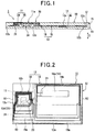
- a dual IC card 1 is provided with a plate-like card body 10 having a recess 11 formed therein, and an IC module 30 accommodated in the recess 11.
- Fig. 1 is a schematic cross-sectional view illustrating the dual IC card 1 in which the number of times of looping an antenna 13 described later is indicated being simplified.
- Fig. 2 illustrates the antenna 13 and a capacitive element 14 in the card body 10 in a transparent manner with only the outline of a substrate 12 being shown.
- the card body 10 includes the substrate 12, the antenna 13 provided on a first surface 12a in which an opening 11a of the recess 11 of the substrate 12 is formed, the capacitive element 14 connected (electrically connected) to the antenna 13, and a pair of card bases 15 sandwiching therebetween the substrate 12, the antenna 13, and the capacitive element 14.
- the substrate 12 is formed into a rectangular shape as viewed perpendicularly from above, using an insulating material, such as PET (polyethylene terephthalate) or polyethylene naphthalate (PEN) (see Fig. 2 ).
- an insulating material such as PET (polyethylene terephthalate) or polyethylene naphthalate (PEN) (see Fig. 2 ).
- PET polyethylene terephthalate
- PEN polyethylene naphthalate
- Each of the card bases 15 is also formed into a rectangular shape as viewed perpendicularly from above.
- an accommodation hole 12d is formed through the substrate 12 in a thickness direction D thereof.
- the accommodation hole 12d is formed into a rectangular shape, with its sides being parallel to the short and long sides of the substrate 12 as viewed perpendicularly from above.
- the substrate 12 has a thickness of 15 to 50 ⁇ m (micrometers).
- the antenna 13 includes a coupling coil 18 to be electromagnetically coupled to a connecting coil 31, described later, of the IC module 30, and a main coil 19 connected to the coupling coil 18 to achieve contactless communication with an external contactless machine (not shown), such as a reader/writer.
- the coupling coil 18 is located in a region R1 in Fig. 2
- the main coil 19 is located in a region R2 adjacent to the region R1. At a position closer to a long side 12e of the substrate 12 than to the accommodation hole 12d (i.e.
- embossed region R3 where an emboss can be provided, in conformity with a standard for IC cards (X 6302-1: 2005 (ISO/I EC 7811-1: 2002)).
- the coupling coil 18 is formed into a helical shape, being looped five times around the accommodation hole 12d.
- the embossed region R3 is provided with a wire 18a configuring the coupling coil 18 and having a width larger than that of a wire 18b located outside the embossed region R3.
- the wire 18b has an end located innermost of the coupling coil 18.
- the innermost end is provided with a terminal portion 20 having a width larger than that of the wire 18b and formed into a substantially circular shape.
- the terminal portion 20 is formed on the first surface 12a.
- the main coil 19 is formed into a helical shape, being looped three times in the region R2.
- the main coil 19 located in the embossed region R3 is configured by a wire 19a having a width larger than that of a wire 19b outside the embossed region R3. Since the widths of the wire 19a and the above wire 18a are made larger, the wires 18a and 19a are prevented from being disconnected when an emboss is provided to the embossed region R3.
- the wire 19a has an end located outermost of the main coil 19. The outermost end is connected to an end of the wire 18a, the end being located outermost of the coupling coil 18.
- the coupling coil 18 and the main coil 19 are formed by etching a copper foil or an aluminum foil into a pattern.
- the coupling coil 18 and the main coil 19 have a thickness, for example, of 5 to 50 ⁇ m.
- the capacitive element 14 includes an electrode plate 14a provided on the first surface 12a of the substrate 12 and an electrode plate 14b provided on a second surface 12b of the substrate 12.
- the electrode plates 14a and 14b are arranged so as to face each other sandwiching the substrate 12.
- the electrode plate 14a is connected to an end located innermost of the wire 19b of the main coil 19.
- connecting wiring 21 provided on the second surface 12b is connected to the electrode plate 14b.
- the connecting wiring 21 extends to a portion facing the terminal portion 20 located on the second surface 12b of the substrate 12, the portion being provided with a terminal portion, not shown.
- the terminal portion 20 of the coupling coil 18 and the terminal portion of the connecting wiring 21 are electrically connected by performing a known crimping process.
- the capacitive element 14 is connected in series between the coupling coil 18 and the main coil 19.
- the card bases 15 are formed of an insulating and durable material.
- Materials that can be used for the bases include polyester-based materials such as amorphous polyester, vinyl chloride-based materials such as PVC (polyvinyl chloride), polycarbonate-based materials, and PET-G (polyethylene terephthalate copolymer).
- the recess 11 is formed in the card bases 15.
- the recess 11 has a first accommodation portion 24 formed in a side face of the card base 15, and a second accommodation portion 25 formed in the bottom surface of the first accommodation portion 24 and having a diameter smaller than that of the first accommodation portion 24.
- the first accommodation portion 24 has an opening positioned on the side face of the card base 15, the opening being the opening 11a mentioned above.
- the IC module 30 is provided with a sheet-like module base (base) 33, an IC chip 34 and the connecting coil 31 which are provided on a first surface 33a of the module base 33, a plurality of contact terminals (contact terminal portions) 35 and a bridge (bridge wiring) 36 provided on a second surface 33b of the module base 33.
- the module base 33 is formed into a rectangular shape, as viewed perpendicularly from above, using the same material as that of the substrate 12.
- a first through hole 33c and a second through hole 33d are formed, being spaced apart from each other and being positioned overlapping with the bridge 36 as viewed in a thickness direction D.
- the thickness direction of the module base 33 coincides with the thickness direction D of the substrate 12 mentioned above.
- through holes (auxiliary through holes) 33e are formed, besides the through holes 33c and 33d.
- the module base 33 has a thickness of 50 to 200 ⁇ m.
- the IC chip 34 an IC chip having a known configuration with a contact communication function and a contactless communication function may be used.
- the IC chip 34 has a chip body 34a whose outer surface is formed with a first terminal 34b, a second terminal 34c, and a plurality of connection terminals 34d.
- the connecting coil 31 is formed into a helical shape.
- the connecting coil 31 is looped three times around the IC chip 34 and the through holes 33c and 33e.
- the second through hole 33d is formed outside the connecting coil 31.
- the connecting coil 31 has a wire end (first end) located outermost and a wire end (second end) located innermost, the wire ends being provided with terminal portions 39 and 40, respectively, which are each formed so as to have a width larger than that of the wire.
- the connecting coil 31 is formed by etching a copper foil or an aluminum foil into a pattern.
- the connecting coil 31 has a thickness of 5 to 50 ⁇ m.
- the connecting coil 31 configures a contactless terminal portion by electromagnetic coupling with the coupling coil 18 of the card body 10.
- the connecting coil 31 formed into a helical shape may be configured with a one-loop coil or may be configured with a helical coil which is looped several times (a plurality of times of looping).
- the plurality of contact terminals 35 and the bridge 36 are formed into a predetermined pattern by laminating a copper foil, for example, on the second surface 33b of the module base 33.
- the bridge 36 is formed into an L shape across the connecting coil 31 as viewed in the thickness direction D (see Fig. 5 ).
- the plurality of contact terminals 35 and the bridge 36 are electrically insulated from each other.
- the area exposed to the outside in the copper foil may be provided with a nickel layer having a thickness of 0.5 to 3 ⁇ m by plating and may further be provided with a gold layer having a thickness of 0.01 to 0.3 ⁇ m on the nickel layer by plating.
- the contact terminals 35 are brought into contact with an external contact machine, such as an automatic teller machine.
- the contact terminals 35 are connected to elements and the like, not shown, built in the chip body 34a of the IC chip 34.
- the plurality of contact terminals may be formed on the second surface 33b of the module base 33 using a lead frame having a thickness of 50 to 200 ⁇ m, and the connecting coil may be formed on the first surface 33a of the module base 33 using a copper wire.
- the first terminal 34b of the IC chip 34 and the bridge 36 are connected via a first wire (first conductive wire) 41 which is inserted through the first through hole 33c.
- the bridge 36 and the terminal portion 39 of the connecting coil 31 are connected via a second wire (second conductive wire) 42 which is inserted through the second through hole 33d.
- the terminal portion 40 of the connecting coil 31 and the second terminal 34c of the IC chip 34 are connected via a third wire (third conductive wire) 43.
- connection terminals 34d of the IC chip 34 and the contact terminals 35 are connected via respective connecting wires (auxiliary conductive wires) 44 that are inserted through the through holes 33e.
- the wires 41, 42, and 43 and the connecting wires 44 are formed of gold or copper and each have an outer diameter of 10 to 40 ⁇ m, for example.
- a closed circuit is configured by the IC chip 34, the connecting coil 31, the bridge 36, and the wires 41, 42, 43, and 44.
- connection terminals 34d of the IC chip 34 In connecting the connection terminals 34d of the IC chip 34 to the contact terminals 35 as well, hole-punching wire bonding is performed using the connecting wires 44.
- wire bonding is performed using the third wire 43.
- a resin seal 51 may be provided, in addition to the components of the IC module 30, to cover the IC chip 34, the first wire 41, the third wire 43, and the connecting wires 44.
- Fig. 7 illustrates, in a transparent manner, the resin seal 51 by a dash double-dotted line.
- the resin seal 51 may be formed of a known epoxy resin, for example.
- the IC module 30A By providing the IC module 30A with the resin seal 51, the IC chip 34 can be protected, and the wires 41 and 43 can be prevented from being disconnected.
- At least part of the first through hole 33c may be ensured to be internally sealed by the resin seal 51. With this configuration, the wire 41 can be prevented from being detached or being disconnected. Further, the first through hole 33c may be entirely sealed by the resin seal 51.
- At least part of or the entire second through hole 33d may be internally sealed by the resin. With this configuration, the wire 42 can be prevented from being detached or being disconnected.
- part of the connecting coil 31 may be bent towards the IC chip 34 to arrange the second through hole 33d inside the inner perimeter of the connecting coil 31.
- the second wire 42 inserted through the second through hole 33d is ensured to be covered (sealed) with the resin seal 51 (see Fig. 9 ).
- all the through holes 33c, 33d, and 33e are covered with the resin seal 51.
- a bridge 56 is formed into a linear shape (see Fig. 10 ).
- the wires 41, 42, and 43 can be prevented from being disconnected.
- At least part of the first and second through holes 33c and 33d may be internally sealed by the resin seal 51. With this configuration, the wires are prevented from being detached or being disconnected. Further, the first and second through holes 33c and33d may be entirely sealed by the resin seal 51.
- the size of the resin seal 51 is preferably small, as long as the resin seal 51 can cover the IC chip 34 as well as the wires 41, 42 and 43, and has a specific strength.
- the resin seal 51 does not have to be made so large as to cover the entire connecting coil 31.
- the following description sets forth a method for manufacturing the IC module 30 configured as above.
- the connecting coil 31 and terminal portions 39 and 40 are formed on the first surface 33a of the module base 33 (the terminal portion 40 is not shown).
- the connecting coil 31 is formed, for example, by performing a known etching process with respect to a copper foil attached to the first surface 33a of the module base 33, followed by forming a specific pattern in in the copper foil.
- the through holes 33c, 33d, and 33e are not shown separated from each other are formed by, for example, performing a known punching process.
- the through holes 33c, 33d, and 33e may be formed firstly in the module base 33, followed by forming the connecting coil 31 on the module base 33.
- the plurality of contact terminals 35 and the bridge 36 are formed on the second surface 33b of the module base 33.
- the contact terminals 35 and the bridge 36 are formed by laminating a copper foil on the second surface 33b of the module base 33, the copper foil being formed with the specific pattern in advance.
- the copper foil is positioned so that the bridge 36 overlaps with the through holes 33c and 33d as viewed in the thickness direction D.
- the IC chip 34 is mounted to the first surface 33a of the module base 33.
- a known die attach adhesive is favorably used.
- the connecting coil 31, the IC chip 34, the plurality of contact terminals 35, and the bridge 36 are then connected by performing known hole-punching wire bonding or wire bonding using the wires 41, 42, 43, and 44.
- the first terminal 34b of the IC chip 34 and the bridge 36 are connected via the first wire 41 inserted through the through hole 33c.
- the bridge 36 and the terminal portion 39 of the connecting coil 31 are connected via the second wire 42 inserted through the second through hole 33d.
- the terminal portion 40 of the connecting coil 31 and the second terminal 34c of the IC chip 34 are connected via the third wire 43.
- connection terminals 34d of the IC chip 34 and the contact terminals 35 are connected via the respective connecting wires 44 inserted through the through holes 33e.
- the IC module 30 is manufactured by the above procedure.
- the substrate 12 is subjected, for example, to etching which is based on a resist coating method performed by means of generally used gravure printing to thereby form the antenna 13, the capacitive element 14, and the like.
- the substrate 12, the antenna 13, and the capacitive element 14 are sandwiched between the pair of card bases 15, followed by integrating the pair of card bases 15 with each other by means of hot-press lamination or an adhesive. Then, the integrated body is punched into individual cards.
- the recess 11 is formed in the card bases 15 by milling to thereby manufacture the card body 10.
- the card body 10 and the IC module 30 are connected by means of an adhesive, such as a hot melt sheet, not shown, so as to accommodate the IC chip 34 of the IC module 30 in the second accommodation portion 25 of the card body 10, thereby manufacturing the dual IC card 1.
- an adhesive such as a hot melt sheet
- the IC chip 34 and the wires 41, 42, and 43 are sealed with a resin in a mold, not shown, to form the resin seal 51 that covers the IC chip 34 as well as the wires 41, 42, and 43.
- Fig. 15 is an equivalent circuit diagram illustrating the principle of the dual IC card 1.
- a reader/writer (contactless external machine) D10 includes a transmitter/receiver circuit D11 which generates a high frequency signal, not shown.
- the high frequency signal induces a high frequency magnetic field in a transmitter/receiver coil D12.
- the high frequency magnetic field is emitted into a space as a magnetic energy.
- the high frequency magnetic field causes current to pass through a parallel resonant circuit which is configured by the antenna 13 and the capacitive element 14 of the dual IC card 1.
- current is also induced in the coupling coil 18 due to the high frequency magnetic field.
- the amount of current induced in the coupling coil 18 is smaller by at least one order of magnitude than the amount of current induced in the main coil 19. Accordingly, the reception sensitivity is greatly dependent on the characteristics of the main coil 19.
- the signal received by the resonant circuit composed of the main coil 19 and the capacitive element 14 is transmitted to the coupling coil 18. Then, due to the electromagnetic coupling between the coupling coil 18 and the connecting coil 31, the signal is transmitted to the IC chip 34.
- a closed circuit is configured by performing hole-punching wire bonding or wire bonding without applying a through-hole plating process to the IC chip 34, the connecting coil 31 and the bridge 36, as well as the wires 41, 42, and 43. Accordingly, the module base 33 does not have to be subjected to plating in manufacturing the IC module 30, and thus the IC module 30 can be easily manufactured at low cost.
- the IC chip 34 and the contact terminals 35 are connected by the connecting wires 44 which are inserted through the respective through holes 33e formed in the module base 33.
- the IC module 30 can be manufactured at lower cost.
- the wires 41, 42 and 43 (first, second, and third conductive wires) with the resin seal 51, the IC chip 34 can be protected and also the wires 41, 42 and 43 can be prevented from being disconnected.
- the IC module 30 can be easily manufactured at low cost. Therefore, the dual IC card 1 including the IC module 30 as a whole can also be easily manufactured at low cost.
- the main coil 19 and the connecting coil 31 are looped three times and the coupling coil 18 is looped five times.
- the number of times of looping these coils 18, 19, and 31 is not limited to the above, but these coils may be looped one or more number of times.
- the number of contact terminals 35 included in the contact terminal portion does not have to be two or more but may be one.
- the IC module 30 is provided in the dual IC card 1.
- the IC module 30 may be provided to an inlet, or a booklet such as a passport.
- a recess is formed in the center of the back cover, a coupling coil is provided around the recess, and a main coil is provided on an edge portion of the back cover.
Landscapes
- Engineering & Computer Science (AREA)
- Computer Hardware Design (AREA)
- Microelectronics & Electronic Packaging (AREA)
- Physics & Mathematics (AREA)
- General Physics & Mathematics (AREA)
- Theoretical Computer Science (AREA)
- Computer Networks & Wireless Communication (AREA)
- Credit Cards Or The Like (AREA)
- Manufacturing & Machinery (AREA)
Abstract
Description
- The present invention relates to an IC module and a dual IC card which are capable of contact communication and contactless communication, and relates to a method for manufacturing an IC module.
- This application claims priority from Japanese Patent Application No.
2013-132898 filed in Japan on June 25, 2013 - IC modules mounting IC chips and having functions of contact communication and contactless communication provide communication modes according to users' various applications. Specifically, such an IC module is mounted to a card body that is capable of power supply and communication by being electromagnetically coupled with the IC module, for use as a dual IC card. Electrical connection between the IC module and the card body by electromagnetic coupling can minimize destabilization of electrical connection between the IC module and the card body. This is because if the IC module and the card body are directly connected by a conductive connecting member, such as solder, the connecting member may be broken when the dual IC card is bent.
- As such a dual IC card in which the IC module and the card body are electrically connected by electromagnetic coupling, there are known the dual IC cards described, for example, in PTLs 1 through 3.
- An IC module for such a dual IC card has a surface on which a terminal used for an interface (contact terminal portion) is formed for contact with an external contact machine, and a rear surface on which a connecting coil is formed for transformer coupling (electromagnetic coupling). The IC module has a base which is subjected to a through-hole plating process to form a bridge (bridge wiring) on the surface of the base, so that the outermost end of the connecting coil is moved to the center of the base. Such a through-hole plating process herein refers to forming a through hole in the base by punching or the like and forming wiring in the through hole by plating or the like.
- The terminal on the surface of the base and the IC chip on the rear surface are connected by hole-punching wire bonding, which is a known wire bonding process using a wire inserted through a through hole of a base.
- Contact communication dual IC cards are used for applications that need reliability and security, such as large quantities of data exchange by credit-card transactions or communication for account settlement procedures. In contrast, contactless communication dual IC cards are used for applications where communication data volume is small and main communication is authentication, such as gate control for allowing someone to enter or leave a room.
-
- PTL 1:
WO 99/26195 - PTL 2:
WO 98/15916 - PTL 3:
WO 96/35190 - However, in the connection method using a through-hole plating process, the base is required to be plated. For this reason, the IC module manufacturing process becomes complicated, which increases the manufacturing cost of the IC module.
- The present invention has been made in light of such problems and has an object to provide an IC module that can be manufactured easily at low cost without plating, and to provide a dual IC card having the IC module and a method for manufacturing the IC module.
- In order to solve the problems set forth above, the invention proposes the following means.
- An IC module according to a first aspect of the present invention includes: a sheet-like base having a first surface and a second surface and having a first through hole and a second through hole spaced apart from the first through hole; an IC chip provided on the first surface, having a contact communication function and a contactless communication function, and having a first terminal and a second terminal formed thereon; a connecting coil formed on the first surface and having a first end and a second end; a contact terminal portion provided on the second surface and configured to contact an external contact machine; bridge wiring provided on the second surface, provided at a position overlapping with the first through hole and the second through hole as viewed in a thickness direction of the base, and electrically insulated from the contact terminal portion; a first conductive wire inserted through the first through hole and connecting the first terminal of the IC chip to the bridge wiring; a second conductive wire inserted through the second through hole and connecting the bridge wiring to the first end of the connecting coil; and a third conductive wire connecting the second end of the connecting coil to the second terminal of the IC chip.
- In the first aspect, the IC chip and the contact terminal portion may be connected via an auxiliary conductive wire inserted through an auxiliary through hole formed in the base.
- In the first aspect, the module may include a resin seal covering the IC chip, the first conductive wire, the second conductive wire, and the third conductive wire.
- A dual IC card according to a second aspect of the present invention includes: the IC module according to the first aspect; and a plate-like card body provided with an antenna having a coupling coil electromagnetically coupled to the connecting coil of the IC module, and a main coil connected to the coupling coil to perform contactless communication with an external contactless machine, the card body having a recess formed therein to accommodate the IC module.
- A method for manufacturing an IC module according to a third aspect of the present invention includes: preparing a sheet-like base having a first surface and a second surface; forming a connecting coil on the first surface; forming, in the base, a first through hole and a second through hole spaced apart from each other; forming, on the second surface, a contact terminal portion configured to contact an external contact machine; forming, on the second surface, bridge wiring electrically insulated from the contact terminal portion, the bridge wiring overlapping with the first through hole and the second through hole as viewed in a thickness direction of the base; mounting, on the first surface of the base, an IC chip having a contact communication function and a contactless communication function; connecting the first terminal of the IC chip to the bridge wiring via a first conductive wire inserted through the first through hole; connecting the bridge wiring to a first end of the connecting coil via a second conductive wire inserted through the second through hole; and connecting a second end of the connecting coil to the second terminal of the IC chip via a third conductive wire.
- In the third aspect, the method may include: forming an auxiliary through hole in the base; and connecting the IC chip to the contact terminal portion via an auxiliary conductive wire inserted through the auxiliary through hole.
- In the third aspect, the method may include covering the IC chip, the first conductive wire, the second conductive wire, and the third conductive wire with a resin seal.
- According to the IC module, the dual IC card, and the method for manufacturing an IC module related to the above aspects, an IC module and a dual IC card can be easily manufactured at low cost without performing a through-hole plating process.
-
-
Fig. 1 is a schematic cross-sectional view illustrating a side face of a dual IC card according to an embodiment of the present invention; -
Fig. 2 is a partially transparent plan view illustrating a card body of the dual IC card according to the embodiment of the present invention; -
Fig. 3 is a plan view illustrating an IC module of the dual IC card according to the embodiment of the present invention; -
Fig. 4 is a cross-sectional view taken along a line A1-A1 ofFig. 3 ; -
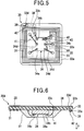
Fig. 5 is a bottom view illustrating the IC module according to the embodiment of the present invention; -
Fig. 6 is a cross-sectional view illustrating a side face of a dual IC card according to a first modification of the embodiment of the present invention; -
Fig. 7 is a bottom view illustrating the dual IC card according to the first modification of the embodiment of the present invention; -
Fig. 8 is a bottom view illustrating a dual IC card according to a second modification of the embodiment of the present invention; -
Fig. 9 is a cross-sectional view taken along a line A2-A2 ofFig. 8 ; -
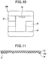
Fig. 10 is a plan view illustrating the dual IC card according to the second modification of the embodiment of the present invention; -
Fig. 11 is a cross-sectional view illustrating a method for manufacturing the IC module according to the embodiment of the present invention; -
Fig. 12 is a cross-sectional view illustrating the method for manufacturing the IC module according to the embodiment of the present invention; -
Fig. 13 is a cross-sectional view illustrating the method for manufacturing the IC module according to the embodiment of the present invention; -
Fig. 14 is a cross-sectional view illustrating the method for manufacturing the IC module according to the embodiment of the present invention; and -
Fig. 15 is an equivalent circuit diagram illustrating the principle of the dual IC card according to the embodiment of the present invention. - With reference to
Figs. 1 to 15 , a dual IC card according to an embodiment of the present invention will be described. - As illustrated in
Figs. 1 and 2 , a dual IC card 1 is provided with a plate-like card body 10 having arecess 11 formed therein, and anIC module 30 accommodated in therecess 11. -
Fig. 1 is a schematic cross-sectional view illustrating the dual IC card 1 in which the number of times of looping anantenna 13 described later is indicated being simplified.Fig. 2 illustrates theantenna 13 and acapacitive element 14 in thecard body 10 in a transparent manner with only the outline of asubstrate 12 being shown. - The
card body 10 includes thesubstrate 12, theantenna 13 provided on afirst surface 12a in which an opening 11a of therecess 11 of thesubstrate 12 is formed, thecapacitive element 14 connected (electrically connected) to theantenna 13, and a pair ofcard bases 15 sandwiching therebetween thesubstrate 12, theantenna 13, and thecapacitive element 14. - The
substrate 12 is formed into a rectangular shape as viewed perpendicularly from above, using an insulating material, such as PET (polyethylene terephthalate) or polyethylene naphthalate (PEN) (seeFig. 2 ). Each of thecard bases 15 is also formed into a rectangular shape as viewed perpendicularly from above. - At a position closer to a
short side 12c of the substrate 12 (than to the center), that is, in a position closer to a short side of thecard bases 15, anaccommodation hole 12d is formed through thesubstrate 12 in a thickness direction D thereof. Theaccommodation hole 12d is formed into a rectangular shape, with its sides being parallel to the short and long sides of thesubstrate 12 as viewed perpendicularly from above. For example, thesubstrate 12 has a thickness of 15 to 50 µm (micrometers). - The
antenna 13 includes acoupling coil 18 to be electromagnetically coupled to a connectingcoil 31, described later, of theIC module 30, and amain coil 19 connected to thecoupling coil 18 to achieve contactless communication with an external contactless machine (not shown), such as a reader/writer. Thecoupling coil 18 is located in a region R1 inFig. 2 , and themain coil 19 is located in a region R2 adjacent to the region R1. At a position closer to along side 12e of thesubstrate 12 than to theaccommodation hole 12d (i.e. than to the center), that is, near the long side of thecard bases 15, there is an embossed region R3 where an emboss can be provided, in conformity with a standard for IC cards (X 6302-1: 2005 (ISO/I EC 7811-1: 2002)). - In this example, the
coupling coil 18 is formed into a helical shape, being looped five times around theaccommodation hole 12d. The embossed region R3 is provided with awire 18a configuring thecoupling coil 18 and having a width larger than that of awire 18b located outside the embossed region R3. Thewire 18b has an end located innermost of thecoupling coil 18. The innermost end is provided with aterminal portion 20 having a width larger than that of thewire 18b and formed into a substantially circular shape. Theterminal portion 20 is formed on thefirst surface 12a. - The
main coil 19 is formed into a helical shape, being looped three times in the region R2. Themain coil 19 located in the embossed region R3 is configured by awire 19a having a width larger than that of awire 19b outside the embossed region R3. Since the widths of thewire 19a and theabove wire 18a are made larger, thewires - The
wire 19a has an end located outermost of themain coil 19. The outermost end is connected to an end of thewire 18a, the end being located outermost of thecoupling coil 18. - The
coupling coil 18 and themain coil 19 are formed by etching a copper foil or an aluminum foil into a pattern. Thecoupling coil 18 and themain coil 19 have a thickness, for example, of 5 to 50 µm. - As illustrated in
Figs. 1 and 2 , thecapacitive element 14 includes anelectrode plate 14a provided on thefirst surface 12a of thesubstrate 12 and anelectrode plate 14b provided on asecond surface 12b of thesubstrate 12. Theelectrode plates substrate 12. - The
electrode plate 14a is connected to an end located innermost of thewire 19b of themain coil 19. - To the
electrode plate 14b, connectingwiring 21 provided on thesecond surface 12b is connected. The connectingwiring 21 extends to a portion facing theterminal portion 20 located on thesecond surface 12b of thesubstrate 12, the portion being provided with a terminal portion, not shown. Theterminal portion 20 of thecoupling coil 18 and the terminal portion of the connectingwiring 21 are electrically connected by performing a known crimping process. Thecapacitive element 14 is connected in series between thecoupling coil 18 and themain coil 19. - The card bases 15 are formed of an insulating and durable material. Materials that can be used for the bases include polyester-based materials such as amorphous polyester, vinyl chloride-based materials such as PVC (polyvinyl chloride), polycarbonate-based materials, and PET-G (polyethylene terephthalate copolymer).
- As illustrated in
Fig. 1 , therecess 11 is formed in the card bases 15. Therecess 11 has afirst accommodation portion 24 formed in a side face of thecard base 15, and asecond accommodation portion 25 formed in the bottom surface of thefirst accommodation portion 24 and having a diameter smaller than that of thefirst accommodation portion 24. Thefirst accommodation portion 24 has an opening positioned on the side face of thecard base 15, the opening being theopening 11a mentioned above. - As illustrated in
Figs. 3 to 5 , theIC module 30 is provided with a sheet-like module base (base) 33, anIC chip 34 and the connectingcoil 31 which are provided on afirst surface 33a of themodule base 33, a plurality of contact terminals (contact terminal portions) 35 and a bridge (bridge wiring) 36 provided on asecond surface 33b of themodule base 33. - The
module base 33 is formed into a rectangular shape, as viewed perpendicularly from above, using the same material as that of thesubstrate 12. In themodule base 33, a first throughhole 33c and a second throughhole 33d are formed, being spaced apart from each other and being positioned overlapping with thebridge 36 as viewed in a thickness direction D. The thickness direction of themodule base 33 coincides with the thickness direction D of thesubstrate 12 mentioned above. In themodule base 33, through holes (auxiliary through holes) 33e are formed, besides the throughholes module base 33 has a thickness of 50 to 200 µm. - As the
IC chip 34, an IC chip having a known configuration with a contact communication function and a contactless communication function may be used. TheIC chip 34 has achip body 34a whose outer surface is formed with afirst terminal 34b, asecond terminal 34c, and a plurality ofconnection terminals 34d. - The connecting
coil 31 is formed into a helical shape. The connectingcoil 31 is looped three times around theIC chip 34 and the throughholes hole 33d is formed outside the connectingcoil 31. The connectingcoil 31 has a wire end (first end) located outermost and a wire end (second end) located innermost, the wire ends being provided withterminal portions coil 31 is formed by etching a copper foil or an aluminum foil into a pattern. For example, the connectingcoil 31 has a thickness of 5 to 50 µm. The connectingcoil 31 configures a contactless terminal portion by electromagnetic coupling with thecoupling coil 18 of thecard body 10. - The connecting
coil 31 formed into a helical shape may be configured with a one-loop coil or may be configured with a helical coil which is looped several times (a plurality of times of looping). - The plurality of
contact terminals 35 and thebridge 36 are formed into a predetermined pattern by laminating a copper foil, for example, on thesecond surface 33b of themodule base 33. Thebridge 36 is formed into an L shape across the connectingcoil 31 as viewed in the thickness direction D (seeFig. 5 ). - The plurality of
contact terminals 35 and thebridge 36 are electrically insulated from each other. The area exposed to the outside in the copper foil may be provided with a nickel layer having a thickness of 0.5 to 3 µm by plating and may further be provided with a gold layer having a thickness of 0.01 to 0.3 µm on the nickel layer by plating. - The
contact terminals 35 are brought into contact with an external contact machine, such as an automatic teller machine. Thecontact terminals 35 are connected to elements and the like, not shown, built in thechip body 34a of theIC chip 34. - The plurality of contact terminals may be formed on the
second surface 33b of themodule base 33 using a lead frame having a thickness of 50 to 200 µm, and the connecting coil may be formed on thefirst surface 33a of themodule base 33 using a copper wire. - The first terminal 34b of the
IC chip 34 and thebridge 36 are connected via a first wire (first conductive wire) 41 which is inserted through the first throughhole 33c. Thebridge 36 and theterminal portion 39 of the connectingcoil 31 are connected via a second wire (second conductive wire) 42 which is inserted through the second throughhole 33d. Theterminal portion 40 of the connectingcoil 31 and the second terminal 34c of theIC chip 34 are connected via a third wire (third conductive wire) 43. - In this example, the
connection terminals 34d of theIC chip 34 and thecontact terminals 35 are connected via respective connecting wires (auxiliary conductive wires) 44 that are inserted through the throughholes 33e. Thewires wires 44 are formed of gold or copper and each have an outer diameter of 10 to 40 µm, for example. - Thus, a closed circuit is configured by the
IC chip 34, the connectingcoil 31, thebridge 36, and thewires - In connecting the first terminal 34b of the
IC chip 34 to thebridge 36 and in connecting thebridge 36 to the connectingcoil 31, hole-punching wire bonding is performed by using thewires - In connecting the
connection terminals 34d of theIC chip 34 to thecontact terminals 35 as well, hole-punching wire bonding is performed using the connectingwires 44. When the connectingcoil 31 is connected to the second terminal 34c of theIC chip 34, wire bonding is performed using thethird wire 43. - In the present embodiment, as in an
IC module 30A illustrated inFigs. 6 and7 , aresin seal 51 may be provided, in addition to the components of theIC module 30, to cover theIC chip 34, thefirst wire 41, thethird wire 43, and the connectingwires 44.Fig. 7 illustrates, in a transparent manner, theresin seal 51 by a dash double-dotted line. Theresin seal 51 may be formed of a known epoxy resin, for example. - By providing the
IC module 30A with theresin seal 51, theIC chip 34 can be protected, and thewires - At least part of the first through
hole 33c may be ensured to be internally sealed by theresin seal 51. With this configuration, thewire 41 can be prevented from being detached or being disconnected. Further, the first throughhole 33c may be entirely sealed by theresin seal 51. - Further, at least part of or the entire second through
hole 33d may be internally sealed by the resin. With this configuration, thewire 42 can be prevented from being detached or being disconnected. - As in an
IC module 30B illustrated inFigs. 8 to 10 , part of the connectingcoil 31 may be bent towards theIC chip 34 to arrange the second throughhole 33d inside the inner perimeter of the connectingcoil 31. Thus, thesecond wire 42 inserted through the second throughhole 33d is ensured to be covered (sealed) with the resin seal 51 (seeFig. 9 ). In this case, all the throughholes resin seal 51. In this example, abridge 56 is formed into a linear shape (seeFig. 10 ). - With such a configuration of the
IC module 30B, thewires - At least part of the first and second through
holes resin seal 51. With this configuration, the wires are prevented from being detached or being disconnected. Further, the first and second throughholes 33c and33d may be entirely sealed by theresin seal 51. - The size of the
resin seal 51 is preferably small, as long as theresin seal 51 can cover theIC chip 34 as well as thewires resin seal 51 does not have to be made so large as to cover the entire connectingcoil 31. - The following description sets forth a method for manufacturing the
IC module 30 configured as above. - Firstly, as illustrated in
Fig. 11 , the connectingcoil 31 andterminal portions first surface 33a of the module base 33 (theterminal portion 40 is not shown). The connectingcoil 31 is formed, for example, by performing a known etching process with respect to a copper foil attached to thefirst surface 33a of themodule base 33, followed by forming a specific pattern in in the copper foil. - As illustrated in
Fig. 12 , in the area where the connectingcoil 31 is not formed in themodule base 33, the throughholes holes 33e are not shown) separated from each other are formed by, for example, performing a known punching process. The throughholes module base 33, followed by forming the connectingcoil 31 on themodule base 33. - As illustrated in
Fig. 13 , the plurality ofcontact terminals 35 and thebridge 36 are formed on thesecond surface 33b of themodule base 33. Thecontact terminals 35 and thebridge 36 are formed by laminating a copper foil on thesecond surface 33b of themodule base 33, the copper foil being formed with the specific pattern in advance. The copper foil is positioned so that thebridge 36 overlaps with the throughholes - Then, as illustrated in
Fig. 14 , theIC chip 34 is mounted to thefirst surface 33a of themodule base 33. In mounting theIC chip 34, a known die attach adhesive is favorably used. - As illustrated in
Figs. 4 and5 , the connectingcoil 31, theIC chip 34, the plurality ofcontact terminals 35, and thebridge 36 are then connected by performing known hole-punching wire bonding or wire bonding using thewires IC chip 34 and thebridge 36 are connected via thefirst wire 41 inserted through the throughhole 33c. Thebridge 36 and theterminal portion 39 of the connectingcoil 31 are connected via thesecond wire 42 inserted through the second throughhole 33d. Theterminal portion 40 of the connectingcoil 31 and the second terminal 34c of theIC chip 34 are connected via thethird wire 43. - In this case, the
connection terminals 34d of theIC chip 34 and thecontact terminals 35 are connected via the respective connectingwires 44 inserted through the throughholes 33e. - The
IC module 30 is manufactured by the above procedure. - The
substrate 12 is subjected, for example, to etching which is based on a resist coating method performed by means of generally used gravure printing to thereby form theantenna 13, thecapacitive element 14, and the like. Thesubstrate 12, theantenna 13, and thecapacitive element 14 are sandwiched between the pair ofcard bases 15, followed by integrating the pair ofcard bases 15 with each other by means of hot-press lamination or an adhesive. Then, the integrated body is punched into individual cards. - The
recess 11 is formed in the card bases 15 by milling to thereby manufacture thecard body 10. - As illustrated in
Fig. 1 , thecard body 10 and theIC module 30 are connected by means of an adhesive, such as a hot melt sheet, not shown, so as to accommodate theIC chip 34 of theIC module 30 in thesecond accommodation portion 25 of thecard body 10, thereby manufacturing the dual IC card 1. - In manufacturing the
IC module 30B mentioned above, theIC chip 34 and thewires resin seal 51 that covers theIC chip 34 as well as thewires - Advantageous effects of the dual IC card 1 configured as above will be described.
Fig. 15 is an equivalent circuit diagram illustrating the principle of the dual IC card 1. - A reader/writer (contactless external machine) D10 includes a transmitter/receiver circuit D11 which generates a high frequency signal, not shown. The high frequency signal induces a high frequency magnetic field in a transmitter/receiver coil D12. The high frequency magnetic field is emitted into a space as a magnetic energy.
- In this case, when the dual IC card 1 is placed in the high frequency magnetic field, the high frequency magnetic field causes current to pass through a parallel resonant circuit which is configured by the
antenna 13 and thecapacitive element 14 of the dual IC card 1. In this case, current is also induced in thecoupling coil 18 due to the high frequency magnetic field. However, the amount of current induced in thecoupling coil 18 is smaller by at least one order of magnitude than the amount of current induced in themain coil 19. Accordingly, the reception sensitivity is greatly dependent on the characteristics of themain coil 19. - The signal received by the resonant circuit composed of the
main coil 19 and thecapacitive element 14 is transmitted to thecoupling coil 18. Then, due to the electromagnetic coupling between thecoupling coil 18 and the connectingcoil 31, the signal is transmitted to theIC chip 34. - Although not shown, when power supply and communication are performed between the dual IC card 1 and an external contact machine such as an automatic teller machine, terminals provided to the automatic teller machine are brought into contact with the
contact terminals 35 of the dual IC card 1. Then, power supply and communication are performed between a control unit of the automatic teller machine and theIC chip 34. - As described above, according to the
IC module 30 and the method for manufacturing theIC module 30 of the present embodiment, a closed circuit is configured by performing hole-punching wire bonding or wire bonding without applying a through-hole plating process to theIC chip 34, the connectingcoil 31 and thebridge 36, as well as thewires module base 33 does not have to be subjected to plating in manufacturing theIC module 30, and thus theIC module 30 can be easily manufactured at low cost. - The
IC chip 34 and thecontact terminals 35 are connected by the connectingwires 44 which are inserted through the respective throughholes 33e formed in themodule base 33. By performing hole-punching wire bonding for the connection between theIC chip 34 and thecontact terminals 35 as well, theIC module 30 can be manufactured at lower cost. - By covering the
IC chip 34, thewires resin seal 51, theIC chip 34 can be protected and also thewires - According to the dual IC card 1, the
IC module 30 can be easily manufactured at low cost. Therefore, the dual IC card 1 including theIC module 30 as a whole can also be easily manufactured at low cost. - An embodiment of the present invention has been described so far in detail with reference to the drawings. However, specific configurations are not limited to the above embodiment. The present invention should include modifications and combinations of the configurations within a scope not departing from the spirit of the present invention.
- For example, in the above embodiment, the
main coil 19 and the connectingcoil 31 are looped three times and thecoupling coil 18 is looped five times. However, the number of times of looping thesecoils - The number of
contact terminals 35 included in the contact terminal portion does not have to be two or more but may be one. - In the above embodiment, the
IC module 30 is provided in the dual IC card 1. - However, an object to be provided with the
IC module 30 is not limited to this. For example, theIC module 30 may be provided to an inlet, or a booklet such as a passport. When theIC module 30 is provided to a back cover of a booklet, a recess is formed in the center of the back cover, a coupling coil is provided around the recess, and a main coil is provided on an edge portion of the back cover. -
- 1 Dual IC card
- 10 Card body
- 11 Recess
- 13 Antenna
- 18 Coupling coil
- 19 Main coil
- 30, 30A, 30B IC module
- 31 Connecting coil
- 33 Module base (Base)
- 33a First surface
- 33b Second surface
- 33c First through hole
- 33d Second through hole
- 33e Through hole (Auxiliary through hole)
- 34 IC chip
- 34b First terminal
- 34c Second terminal
- 35 Contact terminal (Contact terminal portion)
- 36, 56 Bridge (Bridge wiring)
- 41 First wire (First conductive wire)
- 42 Second wire (Second conductive wire)
- 43 Third wire (Third conductive wire)
- 44 Connecting wire (Auxiliary conductive wire)
- 51 Resin seal
- D Thickness direction
- D10 Reader/writer
Claims (7)
- An IC module comprising:a sheet-like base having a first surface and a second surface and having a first through hole and a second through hole spaced apart from the first through hole;an IC chip provided on the first surface, having a contact communication function and a contactless communication function, and having a first terminal and a second terminal formed thereon;a connecting coil formed on the first surface and having a first end and a second end;a contact terminal portion provided on the second surface and configured to contact an external contact machine;bridge wiring provided on the second surface, provided at a position overlapping with the first through hole and the second through hole as viewed in a thickness direction of the base, and electrically insulated from the contact terminal portion;a first conductive wire inserted through the first through hole and connecting the first terminal of the IC chip to the bridge wiring;a second conductive wire inserted through the second through hole and connecting the bridge wiring to the first end of the connecting coil; anda third conductive wire connecting the second end of the connecting coil to the second terminal of the IC chip.
- The IC module according to claim 1, wherein the IC chip and the contact terminal portion are connected via an auxiliary conductive wire inserted through an auxiliary through hole formed in the base.
- The IC module according to claim 1 or 2, wherein the module includes a resin seal covering the IC chip, the first conductive wire, the second conductive wire, and the third conductive wire.
- A dual IC card comprising:the IC module according to claim 1; anda plate-like card body provided with an antenna having a coupling coil electromagnetically coupled to the connecting coil of the IC module, and a main coil connected to the coupling coil to perform contactless communication with an external contactless machine, the card body having a recess formed therein to accommodate the IC module.
- A method for manufacturing an IC module, comprising:preparing a sheet-like base having a first surface and a second surface;forming a connecting coil on the first surface;forming, in the base, a first through hole and a second through hole spaced apart from each other;forming, on the second surface, a contact terminal portion configured to contact an external contact machine;forming, on the second surface, bridge wiring electrically insulated from the contact terminal portion, the bridge wiring overlapping with the first through hole and the second through hole as viewed in a thickness direction of the base;mounting, on the first surface of the base, an IC chip having a contact communication function and a contactless communication function;connecting the first terminal of the IC chip to the bridge wiring via a first conductive wire inserted through the first through hole;connecting the bridge wiring to a first end of the connecting coil via a second conductive wire inserted through the second through hole; andconnecting a second end of the connecting coil to the second terminal of the IC chip via a third conductive wire.
- The method for manufacturing an IC module according to claim 5, comprising:forming an auxiliary through hole in the base; andconnecting the IC chip to the contact terminal portion via an auxiliary conductive wire inserted through the auxiliary through hole.
- The method for manufacturing an IC module according to claim 5 or 6, comprising covering the IC chip, the first conductive wire, the second conductive wire, and the third conductive wire with a resin seal.
Applications Claiming Priority (2)
| Application Number | Priority Date | Filing Date | Title |
|---|---|---|---|
| JP2013132898A JP6090006B2 (en) | 2013-06-25 | 2013-06-25 | IC module, dual IC card and IC module manufacturing method |
| PCT/JP2014/066656 WO2014208532A1 (en) | 2013-06-25 | 2014-06-24 | Ic module, dual ic card, and method for producing ic module |
Publications (3)
| Publication Number | Publication Date |
|---|---|
| EP3016032A1 true EP3016032A1 (en) | 2016-05-04 |
| EP3016032A4 EP3016032A4 (en) | 2017-03-15 |
| EP3016032B1 EP3016032B1 (en) | 2021-05-26 |
Family
ID=52141866
Family Applications (1)
| Application Number | Title | Priority Date | Filing Date |
|---|---|---|---|
| EP14817877.5A Active EP3016032B1 (en) | 2013-06-25 | 2014-06-24 | Ic module, dual ic card, and method for producing ic module |
Country Status (5)
| Country | Link |
|---|---|
| US (1) | US9633301B2 (en) |
| EP (1) | EP3016032B1 (en) |
| JP (1) | JP6090006B2 (en) |
| CN (1) | CN105378760B (en) |
| WO (1) | WO2014208532A1 (en) |
Cited By (2)
| Publication number | Priority date | Publication date | Assignee | Title |
|---|---|---|---|---|
| FR3047101A1 (en) * | 2016-01-26 | 2017-07-28 | Linxens Holding | METHOD FOR MANUFACTURING A CHIP CARD MODULE AND A CHIP CARD |
| WO2023118684A1 (en) * | 2021-12-24 | 2023-06-29 | Wisekey Semiconductors | Method for manufacturing contactless module having an antenna coil with finely adjustable inductance |
Families Citing this family (13)
| Publication number | Priority date | Publication date | Assignee | Title |
|---|---|---|---|---|
| ES2590339T3 (en) * | 2008-02-22 | 2016-11-21 | Toppan Printing Co., Ltd. | Transponder and book form |
| JP2016212778A (en) * | 2015-05-13 | 2016-12-15 | 凸版印刷株式会社 | Dual interface communication medium |
| DE102016106698A1 (en) * | 2016-04-12 | 2017-10-12 | Infineon Technologies Ag | Chip card and method for producing a chip card |
| EP3543913B1 (en) * | 2016-11-18 | 2022-05-04 | Toppan Printing Co., Ltd. | Electromagnetic-coupling dual ic card and ic module |
| FR3074335B1 (en) * | 2017-11-24 | 2019-10-18 | Smart Packaging Solutions | ELECTRONIC MODULE WITH OPTIMIZED ANTENNA FOR A CHIP CARD WITH A DOUBLE COMMUNICATION INTERFACE |
| JP7306123B2 (en) * | 2019-07-18 | 2023-07-11 | 凸版印刷株式会社 | IC module, dual IC card, and IC module manufacturing method |
| JP7287184B2 (en) * | 2019-08-27 | 2023-06-06 | 凸版印刷株式会社 | IC module |
| KR102886403B1 (en) * | 2020-09-07 | 2025-11-17 | 엘지이노텍 주식회사 | Circuit board and fingerprint recognition smart card including the same |
| KR102914017B1 (en) * | 2020-09-08 | 2026-01-19 | 엘지이노텍 주식회사 | Smart ic substrate, smart ic module and ic card including the same |
| JP7749989B2 (en) * | 2021-09-06 | 2025-10-07 | Toppanホールディングス株式会社 | IC module board |
| JP7852389B2 (en) * | 2022-06-07 | 2026-04-28 | Toppanホールディングス株式会社 | IC modules and IC cards |
| WO2026037059A1 (en) * | 2024-08-16 | 2026-02-19 | Act Identity Technology Limited | Lead frame, integrated circuit (ic) module, ic card and method of formation |
| WO2026089571A1 (en) * | 2024-10-25 | 2026-04-30 | 엘지이노텍 주식회사 | Circuit board for smart card, smart ic module, and smart card including same |
Family Cites Families (14)
| Publication number | Priority date | Publication date | Assignee | Title |
|---|---|---|---|---|
| JPS63149191A (en) * | 1986-12-15 | 1988-06-21 | 日立マクセル株式会社 | Ic card |
| FR2625000B1 (en) * | 1987-12-22 | 1991-08-16 | Sgs Thomson Microelectronics | CHIP CARD STRUCTURE |
| FR2721732B1 (en) * | 1994-06-22 | 1996-08-30 | Solaic Sa | Contactless memory card whose electronic circuit includes a module. |
| DE19516227C2 (en) | 1995-05-03 | 2002-02-07 | Infineon Technologies Ag | Data carrier arrangement, in particular chip card |
| KR20000049028A (en) | 1996-10-09 | 2000-07-25 | 피에이브이 카드 게엠베하 | Method and connection arrangement for producing a smart card |
| JPH11149536A (en) * | 1997-11-14 | 1999-06-02 | Toppan Printing Co Ltd | Composite IC card |
| CN1179295C (en) | 1997-11-14 | 2004-12-08 | 凸版印刷株式会社 | Composite IC module and composite IC card |
| CA2277119C (en) * | 1997-11-14 | 2003-06-03 | Western Atlas International, Inc. | Seismic data acquisition and processing using non-linear distortion in a groundforce signal |
| IL122250A (en) * | 1997-11-19 | 2003-07-31 | On Track Innovations Ltd | Smart card amenable to assembly using two manufacturing stages and a method of manufacture thereof |
| TWI234252B (en) * | 2003-05-13 | 2005-06-11 | Siliconware Precision Industries Co Ltd | Flash-preventing window ball grid array semiconductor package and chip carrier and method for fabricating the same |
| US7777317B2 (en) * | 2005-12-20 | 2010-08-17 | Assa Abloy Identification Technologies Austria GmbH (Austria) | Card and manufacturing method |
| CN101416206A (en) * | 2006-03-30 | 2009-04-22 | 王子制纸株式会社 | IC module, IC inlet, and IC package |
| JP2009075782A (en) * | 2007-09-19 | 2009-04-09 | Toshiba Corp | IC module and IC card |
| EP2426627B1 (en) * | 2010-09-02 | 2016-10-12 | Oberthur Technologies | Luminous module for a microcircuit device |
-
2013
- 2013-06-25 JP JP2013132898A patent/JP6090006B2/en active Active
-
2014
- 2014-06-24 EP EP14817877.5A patent/EP3016032B1/en active Active
- 2014-06-24 WO PCT/JP2014/066656 patent/WO2014208532A1/en not_active Ceased
- 2014-06-24 CN CN201480033526.8A patent/CN105378760B/en active Active
-
2015
- 2015-12-17 US US14/973,457 patent/US9633301B2/en active Active
Cited By (5)
| Publication number | Priority date | Publication date | Assignee | Title |
|---|---|---|---|---|
| FR3047101A1 (en) * | 2016-01-26 | 2017-07-28 | Linxens Holding | METHOD FOR MANUFACTURING A CHIP CARD MODULE AND A CHIP CARD |
| WO2017129904A1 (en) * | 2016-01-26 | 2017-08-03 | Linxens Holding | Method for manufacturing a smart card module and a smart card |
| US10706346B2 (en) | 2016-01-26 | 2020-07-07 | Linxens Holding | Method for manufacturing a smart card module and a smart card |
| WO2023118684A1 (en) * | 2021-12-24 | 2023-06-29 | Wisekey Semiconductors | Method for manufacturing contactless module having an antenna coil with finely adjustable inductance |
| FR3131411A1 (en) * | 2021-12-24 | 2023-06-30 | Wisekey Semiconductors | Method of manufacturing a contactless module having a finely adjustable inductance antenna coil |
Also Published As
| Publication number | Publication date |
|---|---|
| JP2015007898A (en) | 2015-01-15 |
| US20160104064A1 (en) | 2016-04-14 |
| JP6090006B2 (en) | 2017-03-08 |
| EP3016032B1 (en) | 2021-05-26 |
| WO2014208532A1 (en) | 2014-12-31 |
| CN105378760B (en) | 2019-07-26 |
| CN105378760A (en) | 2016-03-02 |
| EP3016032A4 (en) | 2017-03-15 |
| US9633301B2 (en) | 2017-04-25 |
Similar Documents
| Publication | Publication Date | Title |
|---|---|---|
| EP3016032B1 (en) | Ic module, dual ic card, and method for producing ic module | |
| EP3590075B1 (en) | Chip card and method for fabricating a chip card | |
| EP4042329B1 (en) | Smart cards having led and methods for fabrication thereof | |
| US10679117B2 (en) | Dual IC card | |
| CN103946874B (en) | composite IC card | |
| US20150269477A1 (en) | Dual-interface hybrid metal smartcard with a booster antenna or coupling frame | |
| US11222861B2 (en) | Dual-interface IC card module | |
| US11200479B2 (en) | Electromagnetic-coupling dual IC card and IC module | |
| EP4167133B1 (en) | Card-type medium | |
| JP2018092482A (en) | Ic module, medium mounted with ic module and method for manufacturing ic module | |
| JP7306123B2 (en) | IC module, dual IC card, and IC module manufacturing method | |
| US10936932B2 (en) | Dual IC cards and antenna sheets | |
| JP2018097724A (en) | Ic module, and ic module-mounted medium | |
| JP6225508B2 (en) | Dual IC card | |
| JP2000172814A (en) | Composite IC module and composite IC card | |
| JP2015106331A (en) | Dual ic card | |
| JP2014119784A (en) | Booklet having ic and manufacturing method thereof | |
| JP2019004292A (en) | Dual IC card | |
| CN115146755B (en) | Chip modules and cards | |
| JP7159663B2 (en) | Booster antenna and dual IC card | |
| JP2020095348A (en) | Non-contact communication medium | |
| HK40080857A (en) | Card inlay for direct connection or inductive coupling technology |
Legal Events
| Date | Code | Title | Description |
|---|---|---|---|
| PUAI | Public reference made under article 153(3) epc to a published international application that has entered the european phase |
Free format text: ORIGINAL CODE: 0009012 |
|
| 17P | Request for examination filed |
Effective date: 20151211 |
|
| AK | Designated contracting states |
Kind code of ref document: A1 Designated state(s): AL AT BE BG CH CY CZ DE DK EE ES FI FR GB GR HR HU IE IS IT LI LT LU LV MC MK MT NL NO PL PT RO RS SE SI SK SM TR |
|
| AX | Request for extension of the european patent |
Extension state: BA ME |
|
| DAX | Request for extension of the european patent (deleted) | ||
| A4 | Supplementary search report drawn up and despatched |
Effective date: 20170213 |
|
| RIC1 | Information provided on ipc code assigned before grant |
Ipc: G06K 19/077 20060101AFI20170207BHEP Ipc: G06K 19/07 20060101ALI20170207BHEP |
|
| STAA | Information on the status of an ep patent application or granted ep patent |
Free format text: STATUS: EXAMINATION IS IN PROGRESS |
|
| 17Q | First examination report despatched |
Effective date: 20190318 |
|
| GRAP | Despatch of communication of intention to grant a patent |
Free format text: ORIGINAL CODE: EPIDOSNIGR1 |
|
| STAA | Information on the status of an ep patent application or granted ep patent |
Free format text: STATUS: GRANT OF PATENT IS INTENDED |
|
| INTG | Intention to grant announced |
Effective date: 20210211 |
|
| GRAS | Grant fee paid |
Free format text: ORIGINAL CODE: EPIDOSNIGR3 |
|
| GRAA | (expected) grant |
Free format text: ORIGINAL CODE: 0009210 |
|
| STAA | Information on the status of an ep patent application or granted ep patent |
Free format text: STATUS: THE PATENT HAS BEEN GRANTED |
|
| AK | Designated contracting states |
Kind code of ref document: B1 Designated state(s): AL AT BE BG CH CY CZ DE DK EE ES FI FR GB GR HR HU IE IS IT LI LT LU LV MC MK MT NL NO PL PT RO RS SE SI SK SM TR |
|
| REG | Reference to a national code |
Ref country code: GB Ref legal event code: FG4D |
|
| REG | Reference to a national code |
Ref country code: CH Ref legal event code: EP |
|
| REG | Reference to a national code |
Ref country code: AT Ref legal event code: REF Ref document number: 1396959 Country of ref document: AT Kind code of ref document: T Effective date: 20210615 |
|
| REG | Reference to a national code |
Ref country code: DE Ref legal event code: R096 Ref document number: 602014077757 Country of ref document: DE |
|
| REG | Reference to a national code |
Ref country code: IE Ref legal event code: FG4D |
|
| REG | Reference to a national code |
Ref country code: LT Ref legal event code: MG9D |
|
| REG | Reference to a national code |
Ref country code: AT Ref legal event code: MK05 Ref document number: 1396959 Country of ref document: AT Kind code of ref document: T Effective date: 20210526 |
|
| PG25 | Lapsed in a contracting state [announced via postgrant information from national office to epo] |
Ref country code: FI Free format text: LAPSE BECAUSE OF FAILURE TO SUBMIT A TRANSLATION OF THE DESCRIPTION OR TO PAY THE FEE WITHIN THE PRESCRIBED TIME-LIMIT Effective date: 20210526 Ref country code: LT Free format text: LAPSE BECAUSE OF FAILURE TO SUBMIT A TRANSLATION OF THE DESCRIPTION OR TO PAY THE FEE WITHIN THE PRESCRIBED TIME-LIMIT Effective date: 20210526 Ref country code: BG Free format text: LAPSE BECAUSE OF FAILURE TO SUBMIT A TRANSLATION OF THE DESCRIPTION OR TO PAY THE FEE WITHIN THE PRESCRIBED TIME-LIMIT Effective date: 20210826 Ref country code: AT Free format text: LAPSE BECAUSE OF FAILURE TO SUBMIT A TRANSLATION OF THE DESCRIPTION OR TO PAY THE FEE WITHIN THE PRESCRIBED TIME-LIMIT Effective date: 20210526 Ref country code: HR Free format text: LAPSE BECAUSE OF FAILURE TO SUBMIT A TRANSLATION OF THE DESCRIPTION OR TO PAY THE FEE WITHIN THE PRESCRIBED TIME-LIMIT Effective date: 20210526 |
|
| REG | Reference to a national code |
Ref country code: NL Ref legal event code: MP Effective date: 20210526 |
|
| PG25 | Lapsed in a contracting state [announced via postgrant information from national office to epo] |
Ref country code: PL Free format text: LAPSE BECAUSE OF FAILURE TO SUBMIT A TRANSLATION OF THE DESCRIPTION OR TO PAY THE FEE WITHIN THE PRESCRIBED TIME-LIMIT Effective date: 20210526 Ref country code: NO Free format text: LAPSE BECAUSE OF FAILURE TO SUBMIT A TRANSLATION OF THE DESCRIPTION OR TO PAY THE FEE WITHIN THE PRESCRIBED TIME-LIMIT Effective date: 20210826 Ref country code: PT Free format text: LAPSE BECAUSE OF FAILURE TO SUBMIT A TRANSLATION OF THE DESCRIPTION OR TO PAY THE FEE WITHIN THE PRESCRIBED TIME-LIMIT Effective date: 20210927 Ref country code: RS Free format text: LAPSE BECAUSE OF FAILURE TO SUBMIT A TRANSLATION OF THE DESCRIPTION OR TO PAY THE FEE WITHIN THE PRESCRIBED TIME-LIMIT Effective date: 20210526 Ref country code: SE Free format text: LAPSE BECAUSE OF FAILURE TO SUBMIT A TRANSLATION OF THE DESCRIPTION OR TO PAY THE FEE WITHIN THE PRESCRIBED TIME-LIMIT Effective date: 20210526 Ref country code: LV Free format text: LAPSE BECAUSE OF FAILURE TO SUBMIT A TRANSLATION OF THE DESCRIPTION OR TO PAY THE FEE WITHIN THE PRESCRIBED TIME-LIMIT Effective date: 20210526 Ref country code: IS Free format text: LAPSE BECAUSE OF FAILURE TO SUBMIT A TRANSLATION OF THE DESCRIPTION OR TO PAY THE FEE WITHIN THE PRESCRIBED TIME-LIMIT Effective date: 20210926 Ref country code: GR Free format text: LAPSE BECAUSE OF FAILURE TO SUBMIT A TRANSLATION OF THE DESCRIPTION OR TO PAY THE FEE WITHIN THE PRESCRIBED TIME-LIMIT Effective date: 20210827 |
|
| PG25 | Lapsed in a contracting state [announced via postgrant information from national office to epo] |
Ref country code: NL Free format text: LAPSE BECAUSE OF FAILURE TO SUBMIT A TRANSLATION OF THE DESCRIPTION OR TO PAY THE FEE WITHIN THE PRESCRIBED TIME-LIMIT Effective date: 20210526 |
|
| PG25 | Lapsed in a contracting state [announced via postgrant information from national office to epo] |
Ref country code: SK Free format text: LAPSE BECAUSE OF FAILURE TO SUBMIT A TRANSLATION OF THE DESCRIPTION OR TO PAY THE FEE WITHIN THE PRESCRIBED TIME-LIMIT Effective date: 20210526 Ref country code: SM Free format text: LAPSE BECAUSE OF FAILURE TO SUBMIT A TRANSLATION OF THE DESCRIPTION OR TO PAY THE FEE WITHIN THE PRESCRIBED TIME-LIMIT Effective date: 20210526 Ref country code: DK Free format text: LAPSE BECAUSE OF FAILURE TO SUBMIT A TRANSLATION OF THE DESCRIPTION OR TO PAY THE FEE WITHIN THE PRESCRIBED TIME-LIMIT Effective date: 20210526 Ref country code: CZ Free format text: LAPSE BECAUSE OF FAILURE TO SUBMIT A TRANSLATION OF THE DESCRIPTION OR TO PAY THE FEE WITHIN THE PRESCRIBED TIME-LIMIT Effective date: 20210526 Ref country code: EE Free format text: LAPSE BECAUSE OF FAILURE TO SUBMIT A TRANSLATION OF THE DESCRIPTION OR TO PAY THE FEE WITHIN THE PRESCRIBED TIME-LIMIT Effective date: 20210526 Ref country code: ES Free format text: LAPSE BECAUSE OF FAILURE TO SUBMIT A TRANSLATION OF THE DESCRIPTION OR TO PAY THE FEE WITHIN THE PRESCRIBED TIME-LIMIT Effective date: 20210526 Ref country code: RO Free format text: LAPSE BECAUSE OF FAILURE TO SUBMIT A TRANSLATION OF THE DESCRIPTION OR TO PAY THE FEE WITHIN THE PRESCRIBED TIME-LIMIT Effective date: 20210526 |
|
| REG | Reference to a national code |
Ref country code: CH Ref legal event code: PL |
|
| REG | Reference to a national code |
Ref country code: DE Ref legal event code: R097 Ref document number: 602014077757 Country of ref document: DE |
|
| REG | Reference to a national code |
Ref country code: BE Ref legal event code: MM Effective date: 20210630 |
|
| PLBE | No opposition filed within time limit |
Free format text: ORIGINAL CODE: 0009261 |
|
| STAA | Information on the status of an ep patent application or granted ep patent |
Free format text: STATUS: NO OPPOSITION FILED WITHIN TIME LIMIT |
|
| PG25 | Lapsed in a contracting state [announced via postgrant information from national office to epo] |
Ref country code: MC Free format text: LAPSE BECAUSE OF FAILURE TO SUBMIT A TRANSLATION OF THE DESCRIPTION OR TO PAY THE FEE WITHIN THE PRESCRIBED TIME-LIMIT Effective date: 20210526 Ref country code: LU Free format text: LAPSE BECAUSE OF NON-PAYMENT OF DUE FEES Effective date: 20210624 |
|
| PG25 | Lapsed in a contracting state [announced via postgrant information from national office to epo] |
Ref country code: LI Free format text: LAPSE BECAUSE OF NON-PAYMENT OF DUE FEES Effective date: 20210630 Ref country code: IE Free format text: LAPSE BECAUSE OF NON-PAYMENT OF DUE FEES Effective date: 20210624 Ref country code: CH Free format text: LAPSE BECAUSE OF NON-PAYMENT OF DUE FEES Effective date: 20210630 |
|
| 26N | No opposition filed |
Effective date: 20220301 |
|
| PG25 | Lapsed in a contracting state [announced via postgrant information from national office to epo] |
Ref country code: IS Free format text: LAPSE BECAUSE OF FAILURE TO SUBMIT A TRANSLATION OF THE DESCRIPTION OR TO PAY THE FEE WITHIN THE PRESCRIBED TIME-LIMIT Effective date: 20210926 Ref country code: AL Free format text: LAPSE BECAUSE OF FAILURE TO SUBMIT A TRANSLATION OF THE DESCRIPTION OR TO PAY THE FEE WITHIN THE PRESCRIBED TIME-LIMIT Effective date: 20210526 |
|
| PG25 | Lapsed in a contracting state [announced via postgrant information from national office to epo] |
Ref country code: IT Free format text: LAPSE BECAUSE OF FAILURE TO SUBMIT A TRANSLATION OF THE DESCRIPTION OR TO PAY THE FEE WITHIN THE PRESCRIBED TIME-LIMIT Effective date: 20210526 Ref country code: BE Free format text: LAPSE BECAUSE OF NON-PAYMENT OF DUE FEES Effective date: 20210630 |
|
| PG25 | Lapsed in a contracting state [announced via postgrant information from national office to epo] |
Ref country code: HU Free format text: LAPSE BECAUSE OF FAILURE TO SUBMIT A TRANSLATION OF THE DESCRIPTION OR TO PAY THE FEE WITHIN THE PRESCRIBED TIME-LIMIT; INVALID AB INITIO Effective date: 20140624 |
|
| PG25 | Lapsed in a contracting state [announced via postgrant information from national office to epo] |
Ref country code: CY Free format text: LAPSE BECAUSE OF FAILURE TO SUBMIT A TRANSLATION OF THE DESCRIPTION OR TO PAY THE FEE WITHIN THE PRESCRIBED TIME-LIMIT Effective date: 20210526 |
|
| P01 | Opt-out of the competence of the unified patent court (upc) registered |
Effective date: 20230530 |
|
| PGFP | Annual fee paid to national office [announced via postgrant information from national office to epo] |
Ref country code: DE Payment date: 20230502 Year of fee payment: 10 |
|
| PG25 | Lapsed in a contracting state [announced via postgrant information from national office to epo] |
Ref country code: MK Free format text: LAPSE BECAUSE OF FAILURE TO SUBMIT A TRANSLATION OF THE DESCRIPTION OR TO PAY THE FEE WITHIN THE PRESCRIBED TIME-LIMIT Effective date: 20210526 |
|
| PGFP | Annual fee paid to national office [announced via postgrant information from national office to epo] |
Ref country code: GB Payment date: 20240502 Year of fee payment: 11 |
|
| PGFP | Annual fee paid to national office [announced via postgrant information from national office to epo] |
Ref country code: FR Payment date: 20240509 Year of fee payment: 11 |
|
| PG25 | Lapsed in a contracting state [announced via postgrant information from national office to epo] |
Ref country code: MT Free format text: LAPSE BECAUSE OF FAILURE TO SUBMIT A TRANSLATION OF THE DESCRIPTION OR TO PAY THE FEE WITHIN THE PRESCRIBED TIME-LIMIT Effective date: 20210526 |
|
| PG25 | Lapsed in a contracting state [announced via postgrant information from national office to epo] |
Ref country code: TR Free format text: LAPSE BECAUSE OF FAILURE TO SUBMIT A TRANSLATION OF THE DESCRIPTION OR TO PAY THE FEE WITHIN THE PRESCRIBED TIME-LIMIT Effective date: 20210526 |
|
| REG | Reference to a national code |
Ref country code: DE Ref legal event code: R119 Ref document number: 602014077757 Country of ref document: DE |
|
| GBPC | Gb: european patent ceased through non-payment of renewal fee |
Effective date: 20250624 |
|
| PG25 | Lapsed in a contracting state [announced via postgrant information from national office to epo] |
Ref country code: GB Free format text: LAPSE BECAUSE OF NON-PAYMENT OF DUE FEES Effective date: 20250624 |
|
| PG25 | Lapsed in a contracting state [announced via postgrant information from national office to epo] |
Ref country code: DE Free format text: LAPSE BECAUSE OF NON-PAYMENT OF DUE FEES Effective date: 20260101 |
|
| PG25 | Lapsed in a contracting state [announced via postgrant information from national office to epo] |
Ref country code: FR Free format text: LAPSE BECAUSE OF NON-PAYMENT OF DUE FEES Effective date: 20250630 |