EP3012679A1 - Piezoelectric and electromagnetic type two-dimensional optical deflector and its manufacturing method - Google Patents
Piezoelectric and electromagnetic type two-dimensional optical deflector and its manufacturing method Download PDFInfo
- Publication number
- EP3012679A1 EP3012679A1 EP15190945.4A EP15190945A EP3012679A1 EP 3012679 A1 EP3012679 A1 EP 3012679A1 EP 15190945 A EP15190945 A EP 15190945A EP 3012679 A1 EP3012679 A1 EP 3012679A1
- Authority
- EP
- European Patent Office
- Prior art keywords
- permanent magnet
- layer
- axis
- mirror
- magnetic
- Prior art date
- Legal status (The legal status is an assumption and is not a legal conclusion. Google has not performed a legal analysis and makes no representation as to the accuracy of the status listed.)
- Withdrawn
Links
Images







Classifications
-
- G—PHYSICS
- G02—OPTICS
- G02B—OPTICAL ELEMENTS, SYSTEMS OR APPARATUS
- G02B26/00—Optical devices or arrangements for the control of light using movable or deformable optical elements
- G02B26/08—Optical devices or arrangements for the control of light using movable or deformable optical elements for controlling the direction of light
- G02B26/0816—Optical devices or arrangements for the control of light using movable or deformable optical elements for controlling the direction of light by means of one or more reflecting elements
- G02B26/0833—Optical devices or arrangements for the control of light using movable or deformable optical elements for controlling the direction of light by means of one or more reflecting elements the reflecting element being a micromechanical device, e.g. a MEMS mirror, DMD
- G02B26/0858—Optical devices or arrangements for the control of light using movable or deformable optical elements for controlling the direction of light by means of one or more reflecting elements the reflecting element being a micromechanical device, e.g. a MEMS mirror, DMD the reflecting means being moved or deformed by piezoelectric means
-
- G—PHYSICS
- G02—OPTICS
- G02B—OPTICAL ELEMENTS, SYSTEMS OR APPARATUS
- G02B26/00—Optical devices or arrangements for the control of light using movable or deformable optical elements
- G02B26/08—Optical devices or arrangements for the control of light using movable or deformable optical elements for controlling the direction of light
- G02B26/0816—Optical devices or arrangements for the control of light using movable or deformable optical elements for controlling the direction of light by means of one or more reflecting elements
- G02B26/0833—Optical devices or arrangements for the control of light using movable or deformable optical elements for controlling the direction of light by means of one or more reflecting elements the reflecting element being a micromechanical device, e.g. a MEMS mirror, DMD
- G02B26/085—Optical devices or arrangements for the control of light using movable or deformable optical elements for controlling the direction of light by means of one or more reflecting elements the reflecting element being a micromechanical device, e.g. a MEMS mirror, DMD the reflecting means being moved or deformed by electromagnetic means
-
- G—PHYSICS
- G02—OPTICS
- G02B—OPTICAL ELEMENTS, SYSTEMS OR APPARATUS
- G02B26/00—Optical devices or arrangements for the control of light using movable or deformable optical elements
- G02B26/08—Optical devices or arrangements for the control of light using movable or deformable optical elements for controlling the direction of light
- G02B26/10—Scanning systems
- G02B26/101—Scanning systems with both horizontal and vertical deflecting means, e.g. raster or XY scanners
-
- G—PHYSICS
- G02—OPTICS
- G02B—OPTICAL ELEMENTS, SYSTEMS OR APPARATUS
- G02B26/00—Optical devices or arrangements for the control of light using movable or deformable optical elements
- G02B26/08—Optical devices or arrangements for the control of light using movable or deformable optical elements for controlling the direction of light
- G02B26/10—Scanning systems
- G02B26/105—Scanning systems with one or more pivoting mirrors or galvano-mirrors
-
- G—PHYSICS
- G09—EDUCATION; CRYPTOGRAPHY; DISPLAY; ADVERTISING; SEALS
- G09G—ARRANGEMENTS OR CIRCUITS FOR CONTROL OF INDICATING DEVICES USING STATIC MEANS TO PRESENT VARIABLE INFORMATION
- G09G3/00—Control arrangements or circuits, of interest only in connection with visual indicators other than cathode-ray tubes
- G09G3/02—Control arrangements or circuits, of interest only in connection with visual indicators other than cathode-ray tubes by tracing or scanning a light beam on a screen
- G09G3/025—Control arrangements or circuits, of interest only in connection with visual indicators other than cathode-ray tubes by tracing or scanning a light beam on a screen with scanning or deflecting the beams in two directions or dimensions
Definitions
- the presently disclosed subject matter relates to a two-dimensional optical deflector.
- the optical deflector can be applied as an optical scanner to a laser pico projector, a laser radar, a bar code reader, an area sensor, an adaptive driving beam (ADB) type head lamp, a head-up display (HUD) unit, and other optical apparatuses, to generate scanning light.
- ADB adaptive driving beam
- HUD head-up display
- a two-dimensional optical deflector is constructed by a micro electro mechanical system (MEMS) device manufactured by using semiconductor manufacturing processes and micro machine technology.
- MEMS micro electro mechanical system
- a two-dimensional optical deflector can be constructed by simply combining two one-dimensional optical deflectors each with one mirror; however, in this case, since laser light is reflected twice, once by each mirror, the utilization of laser light is low and the size is large. Therefore, a two-dimensional optical deflector has been constructed by only one mirror, in order to increase the light utilization efficiency of laser beam and reduce the size.
- a first prior art two-dimensional optical deflector with only one mirror has two of the same kinds of piezoelectric actuators (see: Fig. 19 of JP2008-40240A ).
- this two-dimensional optical deflector is constructed by a mirror, a pair of torsion bars coupled to the mirror along an axis (X-axis), an inner frame (movable frame) surrounding the mirror and the torsion bars, inner piezoelectric actuators coupled between the torsion bars and supported by the inner frame via inner coupling portions, serving as cantilevers for rocking the mirror with respect to the X-axis of the mirror, an outer frame (fixed frame) surrounding the inner frame, and outer piezoelectric actuators of a meandering-type coupled between the inner frame and the outer frame, serving as cantilevers for rocking the mirror along another axis (Y-axis) of the mirror.
- the inner piezoelectric actuators are driven by a drive voltage such as 10 V at a relatively high resonant frequency such as 25 kHz for a horizontal scanning, while the outer piezoelectric actuators are driven by a relatively high drive voltage such as 60 V at a relatively low non-resonant frequency such as 60 Hz for a vertical scanning.
- a piezoelectric driving method is used for both of the horizontal scanning and the vertical scanning.
- the high frequency for a horizontal scanning has to be increased to 30 kHz or more, so that it is difficult to make the resonant frequency compatible with the non-resonant frequency.
- the mechanical rigidity of the optical deflector has to be increased. Further, the drive voltage for the vertical scanning is very high.
- the vibration mode of the inner piezoelectric actuators and the vibration mode of the outer piezoelectric actuators easily interact with each other, so that it is difficult to maintain the flexing angle of the mirror by the non-resonant frequency while suppressing the mode interaction. Further, the optimum thickness of the mirror is different from that of the meandering-type outer piezoelectric actuators.
- a second prior art two-dimensional optical deflector with only one mirror has two different-kinds of actuators: piezoelectric actuators and electromagnetic actuators (see: JP2011-64928A & US2011/0063702A1 ).
- this two-dimensional optical deflector is constructed by a movable body and a base for supporting the movable body.
- the movable body is constructed by a mirror, a pair of first torsion bars coupled to the mirror along an axis (X-axis), an inner frame (first movable frame) surrounding the mirror and the first torsion bars, an outer frame (second movable frame) surrounding the inner frame, piezoelectric actuators coupled between the inner frame and the outer frame, serving as cantilevers for rocking the mirror with respect to the X-axis of the mirror, a pair of second torsion bars coupled between the outer frame and the base along another axis (Y-axis) of the mirror, and a coil provided on the rear surface of the outer frame.
- the base has a recess portion in which a permanent magnet surrounded by a pair of yokes is provided.
- the movable body is bonded to the base, so that the movable body can be rocked along the X-axis and the Y-axis of the mirror.
- the piezoelectric actuators are driven by a drive voltage such as 10 V at a relatively high resonant frequency such as 25 kHz for a horizontal scanning.
- a piezoelectric driving method is used for the horizontal scanning.
- a current is supplied to the coil
- Lorentz forces are generated between the current and a magnetic field generated between the yokes of the permanent magnet (see: Fig. 7 of JP2011-64928A & US2011/0063702A1 )
- the mirror is rocked along the Y-axis.
- the current is driven by a relatively low drive voltage at a relatively low non-resonant frequency such as 60 Hz for a vertical scanning.
- an electromagnetic driving method is used for the vertical scanning.
- the Lorentz forces are very large, the flexing angle of the mirror can be large even at the low non-resonant frequency.
- both of the outer frame on which the coil is formed and the permanent magnet have to be increased in size, which would increase the optical deflector in size.
- a two-dimensional optical deflector including: a mirror; two first torsion bars coupled to the mirror along a first axis; an inner frame surrounding the mirror and the first torsion bars; two piezoelectric actuators each coupled between the first torsion bars and supported by an inner coupling portion of the inner frame, adapted to rock the mirror around the first axis; an outer frame surrounding the inner frame; and two second torsion bars coupled between the inner frame and the outer frame along a second axis;
- a first permanent magnet layer is formed on at least a part of a rear-side surface of the inner frame.
- a base supports a rear-side surface of the outer frame.
- a coil is formed at the base opposing the first permanent magnet layer. A magnetic flux generated from the coil interacts with a magnetic flux of the first permanent magnetic layer to rock the mirror around the second axis.
- a method for manufacturing a two-dimensional optical deflector including: forming a mirror, two first torsion bars coupled to the mirror along a first axis, an inner frame surrounding the mirror and the first torsion bars, two piezoelectric actuators each coupled between the first torsion bars and supported by an inner coupling portion of the inner frame, adapted to rock the mirror around the first axis, an outer frame surrounding the inner frame, and two second torsion bars coupled between the inner frame and the outer frame along a second axis, using a monocrystalline silicon substrate; the method includes forming a first magnetic layer on a rear-side surface of the inner frame; performing a first magnetizing process upon at least a first part of the first magnetic layer to form a first permanent magnet layer; and adhering a rear-side surface of the outer frame onto a base including a coil opposing the permanent magnet layer. A magnetic flux generated from the coil interacts with a magnetic flux of the first permanent magnetic layer to rock the mirror around the second axis.
- the optical deflector can be decreased in size.
- FIG. 1 which illustrates an optical scanner including a first embodiment of the two-dimensional optical deflector according to the presently disclosed subject matter
- reference numeral 10 designates a two-dimensional optical deflector
- 20 designates a control unit for controlling the optical deflector 10 by drive voltages V Xa , V Xb , V Ya and V Yb
- 30 designates a laser light source.
- the two-dimensional optical deflector 10 is constructed by a movable body 10A, a package 10B serving as a base for supporting the movable body 10A, and a spacer 10C interposed between the movable body 10A and the package 10B.
- the laser light source 30 is turned on and off by the control unit 20 which also controls the brightness of the laser light source 30.
- the control unit 20 is constructed by a control circuit such as a microcomputer including a central processing unit (CPU), a field programmable gate array (FPGA), a read-only memory (ROM) or a nonvolatile memory, a random access memory (RAM), an input/output (I/O) interface and the like.
- a control circuit such as a microcomputer including a central processing unit (CPU), a field programmable gate array (FPGA), a read-only memory (ROM) or a nonvolatile memory, a random access memory (RAM), an input/output (I/O) interface and the like.
- Fig. 2A is a front-side perspective view of the movable body 10A of Fig. 1
- Fig. 2B is a perspective view of the package 10B and the spacer 10C of Fig. 1 .
- the movable body 10A is constructed by a circular mirror 1 for reflecting incident light L from the laser light source 30, a pair of torsion bars 2a and 2b coupled to the mirror 1 along an X-axis on the plane of the mirror 1 centered at a center O of the mirror 1, an inner frame (movable frame) 3 surrounding the mirror 1 and the torsion bars 2a and 2b for supporting the mirror 1, a semi-ring shaped piezoelectric actuator 4a coupled between the torsion bars 2a and 2b and supported by an inner coupling portion 3a of the inner frame 3, and a semi-ring shaped piezoelectric actuator 4b coupled between the torsion bars 2a and 2b and supported by an inner coupling portion 3b of the inner frame 3.
- the inner frame 3 has a circular inner circumference along the piezoelectric actuators 4a and 4b, and a rectangular outer circumference.
- the flexing direction of the piezoelectric actuator 4a is opposite to that of the piezoelectric actuator 4b, so that the piezoelectric actuators 4a and 4b serve as cantilevers for rocking the mirror 1 around the X-axis.
- the rocking operation of the mirror 1 around the X-axis for the horizontal scanning is carried out by a piezoelectric driving method using the piezoelectric actuators 4a and 4b.
- the movable body 10A includes an outer frame (fixed frame) 5 surrounding the inner frame 3, and a pair of torsion bars 6a and 6b coupled between the inner frame 3 and the outer frame 5 along a Y-axis perpendicular to the X-axis on the plane of the mirror 1 centered at the center 0 of the mirror 1.
- Permanent magnet layers 7a and 7b and a ring-shaped reinforcement rib 7c on the rear side of the movable body 10A will be explained later with reference to Fig. 3 .
- the mirror 1 includes a metal layer made of Au, Pt or Al with a reflective surface.
- the mirror 1 can be square, rectangular, polygonal or elliptical.
- the inner-circumference of the inner frame 3 is adapted to the shape of the mirror 1.
- the torsion bars 2a and 2b have ends coupled to the outer circumference of the mirror 1 and other ends coupled to the inner circumference of the inner frame 3. Therefore, the torsion bars 2a and 2b are twisted by the piezoelectric actuators 4a and 4b to rock the mirror 1 around the X-axis.
- the cross sections of the torsion bars 2a and 2b are of a square shape to have a size of about 80 to 100 ⁇ m in order to increase the maximum breakdown stress of twisting vibration in comparison with a rectangular cross section. Thus, the flexing angle of the mirror 1 along the X-axis can be increased. Note that the torsion bars 2a and 2b can be extended to be coupled to the inner frame 3 to stabilize the rocking operation of the mirror 1 along the X-axis.
- the outer frame 5 is rectangular-framed to surround the inner frame 3 via the torsion bars 6a and 6b.
- the package 10B is a multilayer ceramic package made of high temperature co-fired ceramic (HTCC) in which a coil 8 opposing the permanent magnet layer 7a and 7b is buried.
- the HTCC has good electrical properties, high mechanical strength and good thermal conductivity. Since the coil 8 is buried in the package 10B, the length of the coil 8 can be increased to increase the magnetic flux generated from the coil 8, and also, the optical deflector can further be decreased in size. Note that the coil 8 can be formed on the package 10B.
- the movable body 10A is fixed via the spacer 10C on the package 10B, so that the inner frame 3 along with the mirror 1 can be rocked along the Y-axis and simultaneously, the mirror 1 can be rocked along the X-axis.
- the movable body 10A is bonded to the spacer 10C by adhesives, and then, the spacer 10C is bonded to the package 10B by adhesives. Otherwise, first, the spacer 10C is bonded to the package 10B by adhesives, and then, the movable body 10A is bonded to the spacer 10C.
- the spacer 10C can be constructed by the package 10B; in this case, the spacer 10C is unnecessary.
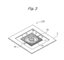
- Fig. 3 is a rear-side perspective view of the movable body 10A of Fig. 1 .
- a permanent magnet layer 7a is formed on a half portion of the rear-side surface of the inner frame 3 on the positive side of the X-axis, while a permanent magnet layer 7b is formed on a half portion of the rear-side surface of the inner frame 3 on the negative side of the X-axis. That is, a boundary between the permanent magnet layers 7a and 7b coincides with the Y-axis.
- the magnetic poles of the permanent magnet layer 7a along the Z-axis are opposite to those of the permanent magnet layer 7b along the Z-axis.
- a ring-shaped reinforcement rib 7c is formed on the rear-side surface of the mirror 1.
- the mirror 1 is so thin that the resonant frequency of the mirror 1 can be increased.
- the ring-shaped reinforcement rib 7c can substantially compensate for the rigidity of the mirror 1.
- the shape of the reinforcement rib 7c can be changed as occasion demands.
- the reinforcement rib 7c can be " figure 8 " shaped.
- the permanent magnet layers 7a and 7b are made of a Nd-Fe-B magnetic material such as Nd 2 Fe 14 B which is magnetized to generate a magnetic flux which is much larger than those of conventional bulk permanent magnets made of magnetic materials such as CoPt. Therefore, the permanent magnet layers 7a and 7b can be very thin, i. e. , about 6 to 10 ⁇ m thick, which would decrease the optical deflector in size.
- the rocking operation of the mirror 1 around the Y-axis for the vertical scanning is carried out by an electromagnetic driving method using the permanent magnet layers 7a and 7b and the coil 8. Since the electromagnetic driving method is not dependent upon the frequency characteristics, the vertical scanning can be carried out at a non-resonant frequency such as 60 Hz.
- the ring-shaped reinforcement is made of the Nd-Fe-B magnetic material such as Nd 2 Fe 14 B, in this case; however, Nd 2 Fe 14 B of the ring-shaped reinforcement rib 7c is not subject to magnetization. Additionally, the specific gravity of Nd 2 Fe 14 B is 7.6, while the specific gravity of Si is 2.3. On the other hand, the rigidity (Young's modulus) of Nd 2 Fe 14 B, that is about 160 GP, is substantially the same as that of Si. Therefore, the ring-shaped reinforcement rib 7c is thin, i. e. , about 6 to 10 ⁇ m. It can correspond to 20 to 30 ⁇ m thickness of silicon. Thus, the ring-shaped reinforcement rib 7c substantially can sufficiently serve as a reinforcement.
- Fig. 4 is a cross-sectional view taken along the line IV-IV in Figs. 2A and 2B where the movable body 10A is bonded via the spacer 10C onto the package 10B.
- the pads P Xa , P Ga , P Xb and P Gb on the outer frame 5 are connected via bonding wires 9a and 9b to pads P Xa ', P Ga ', P Xb ' and P Gb ' on the package 10B and are further connected via interconnects 9a' and 9b' of the package 10B to terminals T Xa , T Ga , T Xb and T Gb on the rear surface of the package 10B.
- the terminals T Xa and T Xb are connected to the control unit 20, while the terminals T Ga and T Gb are grounded.
- the coil 8 is connected via interconnects 9a" and 9b" of the package 10B to terminals T Ya and T Yb on the rear surface of the package 10B.
- the terminals T Ya and T Yb are connected to the control unit 20.
- the permanent magnet layer 7a is magnetized so that the lower surface of the permanent magnet layer 7a serves as an N-pole to generate a downward magnetic flux Ba.
- the permanent magnet layer 7b is magnetized so that the lower surface of the permanent magnet layer 7b serves as an S-pole to generate a downward magnetic flux Bb.
- a magnetic flux Bc is changed in accordance with the alternating current "i". For example, when the magnetic flux Bc is upward, the upper portion of the coil 8 serves as an N-pole.
- the ring-shaped reinforcement rib 7c is made of Nd 2 Fe 14 B, the ring-shaped reinforcement rib 7c is not magnetized, so that the ring-shaped reinforcement rib 7c does not interact with the magnetic flux Bc generated from the coil 8.
- the control unit 20 applies a drive voltage V Xa via the terminal T Xa , the interconnect 9a', the pad P Xa ' and the bonding wire 9a to the pad P Xa and applies a drive voltage V Xb via the terminal T Xb , the interconnect 9b', the pad P Xb ' and the bonding wire 9b to the pad P Xb .
- the drive voltages V Xa and V Xb are sinusoidal, and the drive voltage V X1 is opposite in phase to the drive voltage V Yb .
- the frequency f X of the drive voltages V Xa and V Xb is one resonant frequency f r such as 25 kHz depending upon a resonant structure formed by the mirror 1, the torsion bars 2a and 2b and the piezoelectric actuators 4a and 4b.
- the pad P Xa is connected via the wiring layer 108 (see: Fig. 11L ) to the upper electrode layers 106 (see: Fig. 11L ) of the piezoelectric actuator 4a.
- the pad P Ga which is grounded, is connected via via-structure (not shown) to the lower electrode layer 104 (see: Fig. 11L ) of the piezoelectric actuator 4a.
- the pad P Xb is connected via the wiring layer 108(see: Fig. 11L ) to the upper electrode layers 106 (see: Fig. 11L ) of the piezoelectric actuator 4b.
- the pad P Gb which is grounded, is connected via a via-structure (not shown) to the lower electrode layer 104 (see: Fig. 11L ) of the piezoelectric actuator 4b.
- the control unit 20 applies a drive voltage V Ya from terminal T Ya via an interconnect 9a" to an end of the coil 8, and also, applies a drive voltage V Yb from terminal T Yb via an interconnect 9b" to another end of the coil 8.
- the drive voltages V Ya and V Yb are sinusoidal or saw-tooth-shaped, and the drive voltage V Ya is opposite in phase to the drive voltage V Yb .
- the frequency f Y of the drive voltages V Ya and V Yb is 60Hz, much lower than the resonant frequency f r .
- Figs. 6A , 6B and 6C are rear-side perspective views illustrating modifications of the movable body 10A of Fig. 1 .
- the permanent magnet layer 7b of Fig. 3 is replaced by a non-magnetized layer 7b' which is also made of Nd 2 Fe 14 B. That is, the non-magnetized layer 7b' is not subject to magnetization. Even in this case, the boundary between the permanent magnet layer 7a and the non-magnetized layer 7b' is at the Y-axis. Therefore, a repulsive force or an attractive force occurs only between the N-pole of the permanent magnet layer 7a and the N-pole or S-pole of the coil 8.
- the inner frame 3 can be rocked around the torsion bars 6a and 6b, so that the mirror 1 can be rocked around the Y-axis. Since only the permanent magnet layer 7a is subject to magnetization, the magnetizing process can be simplified so that the manufacturing cost can be decreased.
- Fig. 6B As the area of the permanent magnet layer 7a of Fig. 6A is increased, the boundary between the permanent magnet layer 7a and the non-magnetized layer 7b' is moved toward the negative-side of the Y-axis. Even in this case, a repulsive force or an attractive force occurs only between the N-pole of the permanent magnet layer 7a and the N-pole or S-pole of the coil 8. Since the boundary of the permanent magnet layer 7a and the non-magnetized layer 7b' is not severe, the magnetizing process can further be simplified, so that the manufacturing cost can be further decreased.
- the boundary between the permanent magnet layer 7a and the non-magnetized layer 7b' is preferably at the Y-axis; however, this boundary can be shifted from the Y-axis, i.e., this boundary can be close to the Y-axis and along the Y-axis, which would decrease the manufacturing cost.
- Fig. 7 which illustrates an optical scanner including a second embodiment of the two-dimensional optical deflector according to the presently disclosed subject matter
- the two-dimensional optical deflector 10 of Fig. 1 is replaced by a two-dimensional optical deflector 10'.
- the two-dimensional optical deflector 10' is constructed by a movable body 10A', a package 10B' serving as a base for supporting the movable body 10A', and a spacer 10C' interposed between the movable body 10A' and the package 10B'.
- the package 10B' and the spacer 10C' are shown not in Fig. 7 , but in Fig. 8B .
- the spacer 10C' can be constructed by the package 10B'; in this case, the spacer 10C' is unnecessary.
- Fig. 8A is a front-side perspective view of the movable body 10A' of Fig. 7
- Fig. 8B is a perspective view of the package 10B' and the spacer 10C' of Fig. 7
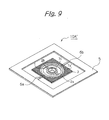
- Fig. 9 is a rear-side perspective view of the movable body 10A' of Fig. 7 .
- Fig. 8B the coil 8 of Fig. 2B is replaced by two coils 8a and 8b whose winding directions are opposite to each other.
- a permanent magnet layers 7a' is formed on the entire rear-side surface of the inner frame 3.
- Fig. 10 is a cross-sectional view taken along the line X-X in Figs. 8A and 8B where the movable body 10A' is bonded via the spacer 10C' onto the package 10B'.
- the coils 8a and 8b opposing the permanent magnet layer 7a' are connected in parallel by interconnects 9a" and 9b" of the package 10B' to the terminals T Ya and T Yb on the rear surface of the package 10B'. Therefore, when the alternating current "i" is supplied to the coils 8a and 8b, the Z-axis direction of a magnetic flux Bca generated from the coil 8a is opposite to that of a magnetic flux Bcb generated from the coil 8b.
- the permanent magnet layer 7a is magnetized so that the lower surface of the permanent magnet layer 7a serves as an N-pole to generate a downward magnetic flux Ba.
- an alternating current "i" whose value is less than 1A
- the magnetic fluxes Bca and Bcb opposite in direction to each other are changed in accordance with the alternating current "i".
- the magnetic fluxes Bca and Bcb are upward and downward, respectively, the upper portion of the coils 8a and 8b serve as an N-pole and an S-pole, respectively.
- Fig. 8B and 10 if the winding direction of the coil 8a is the same as that of the coil 8b, the coils 8a and 8b can be anti-parallelly connected by interconnects of the package 10B' to the terminals T Ya and T Yb .
- a bare monocrystalline silicon wafer (substrate) 101 made of an about 300 ⁇ m thick monocrystalline silicon is prepared. Then, the bare monocrystalline silicon wafer 101 is oxidized by a thermal oxidation process, so that about 1 ⁇ m thick silicon dioxide layers 102 and 103 are formed on both surfaces of the bare monocrystalline silicon wafer 101.
- a Pt/Ti lower electrode layer 104 consisting of an about 50 nm thick Ti and an about 150 nm thick Pt on Ti is formed by a sputtering process.
- an about 3 ⁇ m thick titanate zirconate (PZT) layer 105 is deposited on the lower electrode layer 105 by an arc discharge reactive ion plating (ADRIP) process at a temperature of about 500°C to 600°C.
- ADRIP arc discharge reactive ion plating
- an about 150 nm thick Ti upper electrode layer 106 is formed on the PZT layer 105 by a sputtering process.
- the upper electrode layer 106 and the PZT layer 105 are patterned by a photolithography and etching process.
- the lower electrode layer 104 and the silicon dioxide layer 103 are patterned by a photolithography and etching process.
- an about 500 nm thick silicon dioxide interlayer 107 is formed on the entire surface by a plasma chemical vapor deposition (CVD) process.
- CVD plasma chemical vapor deposition
- contact holes CONT are perforated in the silicon dioxide interlayer 107 by a photolithography and dry etching process.
- the contact holes CONT correspond to the piezoelectric actuators 4a and 4b, the pads P Xa , P Ga , P Xb and P Gb .
- wiring layers 108 made of AlCu (1%Cu) are formed by a photolithography process, a sputtering process, and a lift-off process.
- the wiring layers 108 are electrically connected between the upper electrode layers 106 of the piezoelectric actuators 4a and 4b, and their corresponding pads P Xa , P Ga , P Xb and P Gb .
- an aluminum (Al) reflective metal layer 109 is formed by an evaporation process, and is patterned by a photolithography and etching process.
- trenches TR are formed in the silicon substrate 101 by a deep-reactive ion etching (DRIE) process.
- the trenches TR are used for separating the mirror 1, the torsion bars 2a and 2b, the inner frame 3, the piezoelectric actuators 4a and 4b, the outer frame 5, and the torsion bars 6a and 6b from each other.
- DRIE deep-reactive ion etching
- a wax layer 110 is coated on the entire front surface, and a support wafer 111 is temporarily bonded to the wax layer 110.
- a chemical mechanical polishing (CMP) process is performed upon the entire rear-side surface, so that the silicon substrate 101 becomes about 40 ⁇ m thick. Therefore, the trenches TR are changed to through-holes TH. As a result, the mirror 1, the torsion bars 2a and 2b, the inner frame 3, the piezoelectric actuators 4a and 4b, the outer frame 5, and the torsion bars 6a and 6b are separated from each other.
- CMP chemical mechanical polishing
- a magnetic layer made of Nd 2 Fe 14 B is formed on rear-side surface of the silicon substrate 101 at the mirror 1 and the inner frame 3 by a sputter process using a shadow mask.
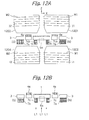
- a magnetizing process is performed upon the magnetic layer, as illustrated in Fig. 12A where a pair of yokes 1201 and 1202 on which a winding W1 for receiving a DC current I1 is placed and a pair of yokes 1203 and 1204 on which a winding W2 for receiving a DC current I2 is placed are provided.
- the direction of the winding W1 is opposite to that of the winding W2.
- the magnetic layer on the positive-side of the X-axis at the inner frame 4a is magnetized to form a permanent magnet layer 7a with an N-pole on the lower surface thereof, while the magnetic layer on the negative-side of the X-axis at the inner frame 3 is magnetized to form a permanent magnet layer 7b with an S-pole on the lower surface thereof.
- the magnetic layer at the mirror 1 may be magnetized, i. e. , the magnetic layer at the mirror 1 may be permanent magnet layers 7ca and 7cb similar to the permanent magnet layers 7a and 7b. In this case, a demagnetizing process is performed upon the magnetic layer at the mirror 1 as illustrated in Fig.
- this magnetic layer is irradiated with laser light L1 to be heated up over its Curie temperature.
- laser light L1 to be heated up over its Curie temperature.
- magnetic dipoles in the magnetic layer on the mirror 1 are dispersed. Therefore, the magnetic layer at the mirror 1 becomes a non-magnetized layer.
- this non-magnetized layer can serves as a ring-shaped reinforcement rib 7c.
- a magnetizing process using only the yokes 1201 and 1202 and the winding W1 for receiving the current I1 is carried out as illustrated in Fig. 13A
- a demagnetizing process is carried out as illustrated in Fig. 13B which is the same as Fig. 12B .
- a magnetizing process using yokes 1401 and 1402 and a winding W3 for receiving the current I3 is carried out as illustrated in Fig. 14A
- a demagnetizing process is carried out as illustrated in Fig. 14B which is the same as Fig. 12B .
- the demagnetizing process as illustrated in Figs. 12B , Fig. 13B and Fig. 14B is unnecessary.
- the outer frame 5 is aligned to the spacer 8 of the package 10B, and then, the outer frame 5 is bonded to a spacer 8 by adhesives. Then, the support wafer 111 is removed.
- the silicon substrate 101 is diced by a stealth dicing method using laser or the like, and each of the diced chips is mounted on a package formed by high temperature co-fired ceramic (HTCC), thus completing the two-dimensional optical deflector of Fig. 1 .
- HTCC high temperature co-fired ceramic
- HD high definition
- the drive voltages V Xa and V Xb for the horizontal scanning were 10 V and the drive voltages V Ya and V Yb for the vertical scanning were 3.3 V. That is, the drive voltages V Ya and V Yb for the vertical scanning can remarkably be reduced as compared with the first prior art two-dimensional optical deflector where the drive voltages for the vertical scanning is 60 V.
Landscapes
- Physics & Mathematics (AREA)
- General Physics & Mathematics (AREA)
- Optics & Photonics (AREA)
- Electromagnetism (AREA)
- Micromachines (AREA)
- Mechanical Optical Scanning Systems (AREA)
- Mechanical Light Control Or Optical Switches (AREA)
Abstract
In a two-dimensional optical deflector including: a mirror (1); two first torsion bars (2a, 2b) coupled to the mirror (1) along a first axis; an inner frame (3) surrounding the mirror (1); two piezoelectric actuators (4a, 4b) each coupled between the first torsion bars (2a, 2b) and supported by the inner frame (3); an outer frame (5) surrounding the inner frame (3); and two second torsion bars (6a, 6b) coupled between the inner frame (3) and the outer frame (5) along a second axis; a first permanent magnet layer (7a, 7a') formed on at least a part of a rear-side surface of the inner frame (3). A base (10B, 10B') supports the outer frame (5). A coil (8, 8a, 8b) is formed at the base (10B, 10B'). A magnetic flux (Bc, Bca) generated from the coil (8, 8a) interacts with a magnetic flux (Ba) of the first permanent magnetic layer (7a, 7a').
Description
- This application claims the priority benefit under 35 U.S.C. §119 to Japanese Patent Application No.
JP2014-216693 filed on October 23, 2014 - The presently disclosed subject matter relates to a two-dimensional optical deflector. The optical deflector can be applied as an optical scanner to a laser pico projector, a laser radar, a bar code reader, an area sensor, an adaptive driving beam (ADB) type head lamp, a head-up display (HUD) unit, and other optical apparatuses, to generate scanning light.
- Generally, in an optical scanner or the like, a two-dimensional optical deflector is constructed by a micro electro mechanical system (MEMS) device manufactured by using semiconductor manufacturing processes and micro machine technology.
- A two-dimensional optical deflector can be constructed by simply combining two one-dimensional optical deflectors each with one mirror; however, in this case, since laser light is reflected twice, once by each mirror, the utilization of laser light is low and the size is large. Therefore, a two-dimensional optical deflector has been constructed by only one mirror, in order to increase the light utilization efficiency of laser beam and reduce the size.
- A first prior art two-dimensional optical deflector with only one mirror has two of the same kinds of piezoelectric actuators (see: Fig. 19 of
JP2008-40240A - In the above-described first prior art two-dimensional optical deflector, the inner piezoelectric actuators are driven by a drive voltage such as 10 V at a relatively high resonant frequency such as 25 kHz for a horizontal scanning, while the outer piezoelectric actuators are driven by a relatively high drive voltage such as 60 V at a relatively low non-resonant frequency such as 60 Hz for a vertical scanning. Thus, a piezoelectric driving method is used for both of the horizontal scanning and the vertical scanning.
- In the above-described first prior art two-dimensional optical deflector; however, in order to enhance the resolution of projected images, the high frequency for a horizontal scanning has to be increased to 30 kHz or more, so that it is difficult to make the resonant frequency compatible with the non-resonant frequency. Also, in this case, in order to suppress the dynamic deformation of the mirror and the spurious vibration of the piezoelectric actuators, the mechanical rigidity of the optical deflector has to be increased. Further, the drive voltage for the vertical scanning is very high.
- Particularly, when the outer piezoelectric actuators are of a meandering-type, the vibration mode of the inner piezoelectric actuators and the vibration mode of the outer piezoelectric actuators easily interact with each other, so that it is difficult to maintain the flexing angle of the mirror by the non-resonant frequency while suppressing the mode interaction. Further, the optimum thickness of the mirror is different from that of the meandering-type outer piezoelectric actuators.
- A second prior art two-dimensional optical deflector with only one mirror has two different-kinds of actuators: piezoelectric actuators and electromagnetic actuators (see:
JP2011-64928A US2011/0063702A1 ). In more detail, this two-dimensional optical deflector is constructed by a movable body and a base for supporting the movable body. The movable body is constructed by a mirror, a pair of first torsion bars coupled to the mirror along an axis (X-axis), an inner frame (first movable frame) surrounding the mirror and the first torsion bars, an outer frame (second movable frame) surrounding the inner frame, piezoelectric actuators coupled between the inner frame and the outer frame, serving as cantilevers for rocking the mirror with respect to the X-axis of the mirror, a pair of second torsion bars coupled between the outer frame and the base along another axis (Y-axis) of the mirror, and a coil provided on the rear surface of the outer frame. On the other hand, the base has a recess portion in which a permanent magnet surrounded by a pair of yokes is provided. The movable body is bonded to the base, so that the movable body can be rocked along the X-axis and the Y-axis of the mirror. - In the second prior art two-dimensional optical deflector, the piezoelectric actuators are driven by a drive voltage such as 10 V at a relatively high resonant frequency such as 25 kHz for a horizontal scanning. Thus, a piezoelectric driving method is used for the horizontal scanning. Contrary to this, when a current is supplied to the coil, Lorentz forces are generated between the current and a magnetic field generated between the yokes of the permanent magnet (see:
Fig. 7 ofJP2011-64928A US2011/0063702A1 ), the mirror is rocked along the Y-axis. The current is driven by a relatively low drive voltage at a relatively low non-resonant frequency such as 60 Hz for a vertical scanning. Thus, an electromagnetic driving method is used for the vertical scanning. In this case, since the Lorentz forces are very large, the flexing angle of the mirror can be large even at the low non-resonant frequency. - In the above-described second prior art two-dimensional optical deflector; however, in order to increase the Lorentz forces, both of the outer frame on which the coil is formed and the permanent magnet have to be increased in size, which would increase the optical deflector in size.
- The presently disclosed subject matter seeks to solve the above-described problems.
- According to the presently disclosed subject matter, in a two-dimensional optical deflector including: a mirror; two first torsion bars coupled to the mirror along a first axis; an inner frame surrounding the mirror and the first torsion bars; two piezoelectric actuators each coupled between the first torsion bars and supported by an inner coupling portion of the inner frame, adapted to rock the mirror around the first axis; an outer frame surrounding the inner frame; and two second torsion bars coupled between the inner frame and the outer frame along a second axis; a first permanent magnet layer is formed on at least a part of a rear-side surface of the inner frame. A base supports a rear-side surface of the outer frame. A coil is formed at the base opposing the first permanent magnet layer. A magnetic flux generated from the coil interacts with a magnetic flux of the first permanent magnetic layer to rock the mirror around the second axis.
- Also, in a method for manufacturing a two-dimensional optical deflector including: forming a mirror, two first torsion bars coupled to the mirror along a first axis, an inner frame surrounding the mirror and the first torsion bars, two piezoelectric actuators each coupled between the first torsion bars and supported by an inner coupling portion of the inner frame, adapted to rock the mirror around the first axis, an outer frame surrounding the inner frame, and two second torsion bars coupled between the inner frame and the outer frame along a second axis, using a monocrystalline silicon substrate; the method includes forming a first magnetic layer on a rear-side surface of the inner frame; performing a first magnetizing process upon at least a first part of the first magnetic layer to form a first permanent magnet layer; and adhering a rear-side surface of the outer frame onto a base including a coil opposing the permanent magnet layer. A magnetic flux generated from the coil interacts with a magnetic flux of the first permanent magnetic layer to rock the mirror around the second axis.
- According to the presently disclosed subject matter, since the permanent magnet layer is provided on the rear-side surface of the inner frame and the coil is provided at the base, the optical deflector can be decreased in size.
- The above and other advantages and features of the presently disclosed subject matter will be more apparent from the following description of certain embodiments, taken in conjunction with the accompanying drawings, wherein:
-
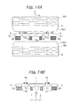
Fig. 1 is a front-side perspective view illustrating an optical scanner including a first embodiment of the two-dimensional optical deflector according to the presently disclosed subject matter; -
Fig. 2A is a front-side perspective view of the movable body ofFig. 1 ; -
Fig. 2B is a perspective view of the package ofFig. 1 ; -
Fig. 3 is a rear-side perspective view of the movable body ofFig. 1 ; -
Fig. 4 is a cross-sectional view taken along the line IV-IV inFigs. 2A and 2B where the movable body ofFig. 2A is bonded onto the package ofFig. 2B ; -
Figs. 5A through 5D are timing diagrams of the drive voltages supplied to the optical deflector ofFig. 1 ; -
Figs. 6A ,6B and 6C are rear-side perspective views illustrating modifications of the movable body ofFig. 1 ; -
Fig. 7 is a front-side perspective view illustrating an optical scanner including a second embodiment of the two-dimensional optical deflector according to the presently disclosed subject matter; -
Fig. 8A is a front-side perspective view of the movable body ofFig. 7 ; -
Fig. 8B is a perspective view of the package ofFig. 7 ; -
Fig. 9 is a rear-side perspective view of the movable body ofFig. 7 ; -
Fig. 10 is a cross-sectional view taken along the line X-X inFigs. 8A and 8B where the movable body ofFig. 8A is bonded onto the package ofFig. 8B ; -
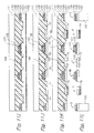
Figs. 11A through 11L are cross-sectional views for explaining a method for manufacturing the two-dimensional optical deflector ofFig. 1 ; and -
Figs. 12A and 12B ,Figs. 13A and 13B , andFigs. 14A and 14B are cross-sectional views for explaining the magnetizing and demagnetizing processes ofFig. 11L . - In
Fig. 1 , which illustrates an optical scanner including a first embodiment of the two-dimensional optical deflector according to the presently disclosed subject matter,reference numeral 10 designates a two-dimensional optical deflector, 20 designates a control unit for controlling theoptical deflector 10 by drive voltages VXa, VXb, VYa and VYb, and 30 designates a laser light source. The two-dimensionaloptical deflector 10 is constructed by amovable body 10A, apackage 10B serving as a base for supporting themovable body 10A, and aspacer 10C interposed between themovable body 10A and thepackage 10B. Thelaser light source 30 is turned on and off by thecontrol unit 20 which also controls the brightness of thelaser light source 30. - The
control unit 20 is constructed by a control circuit such as a microcomputer including a central processing unit (CPU), a field programmable gate array (FPGA), a read-only memory (ROM) or a nonvolatile memory, a random access memory (RAM), an input/output (I/O) interface and the like. -
Fig. 2A is a front-side perspective view of themovable body 10A ofFig. 1 , andFig. 2B is a perspective view of thepackage 10B and thespacer 10C ofFig. 1 . - Referring to
Figs. 1 and2A , themovable body 10A is constructed by acircular mirror 1 for reflecting incident light L from thelaser light source 30, a pair oftorsion bars mirror 1 along an X-axis on the plane of themirror 1 centered at a center O of themirror 1, an inner frame (movable frame) 3 surrounding themirror 1 and thetorsion bars mirror 1, a semi-ring shapedpiezoelectric actuator 4a coupled between thetorsion bars inner frame 3, and a semi-ring shapedpiezoelectric actuator 4b coupled between thetorsion bars inner coupling portion 3b of theinner frame 3. In this case, theinner frame 3 has a circular inner circumference along thepiezoelectric actuators piezoelectric actuator 4a is opposite to that of thepiezoelectric actuator 4b, so that thepiezoelectric actuators mirror 1 around the X-axis. - Thus, the rocking operation of the
mirror 1 around the X-axis for the horizontal scanning is carried out by a piezoelectric driving method using thepiezoelectric actuators - Also, the
movable body 10A includes an outer frame (fixed frame) 5 surrounding theinner frame 3, and a pair oftorsion bars inner frame 3 and theouter frame 5 along a Y-axis perpendicular to the X-axis on the plane of themirror 1 centered at the center 0 of themirror 1. - Permanent magnet layers 7a and 7b and a ring-shaped
reinforcement rib 7c on the rear side of themovable body 10A will be explained later with reference toFig. 3 . - In more detail, the
mirror 1 includes a metal layer made of Au, Pt or Al with a reflective surface. Themirror 1 can be square, rectangular, polygonal or elliptical. In this case, the inner-circumference of theinner frame 3 is adapted to the shape of themirror 1. - The torsion bars 2a and 2b have ends coupled to the outer circumference of the
mirror 1 and other ends coupled to the inner circumference of theinner frame 3. Therefore, thetorsion bars piezoelectric actuators mirror 1 around the X-axis. The cross sections of thetorsion bars mirror 1 along the X-axis can be increased. Note that thetorsion bars inner frame 3 to stabilize the rocking operation of themirror 1 along the X-axis. - The
outer frame 5 is rectangular-framed to surround theinner frame 3 via thetorsion bars - Referring to
Fig. 2B , thepackage 10B is a multilayer ceramic package made of high temperature co-fired ceramic (HTCC) in which acoil 8 opposing thepermanent magnet layer coil 8 is buried in thepackage 10B, the length of thecoil 8 can be increased to increase the magnetic flux generated from thecoil 8, and also, the optical deflector can further be decreased in size. Note that thecoil 8 can be formed on thepackage 10B. - The
movable body 10A is fixed via thespacer 10C on thepackage 10B, so that theinner frame 3 along with themirror 1 can be rocked along the Y-axis and simultaneously, themirror 1 can be rocked along the X-axis. For example, first, themovable body 10A is bonded to thespacer 10C by adhesives, and then, thespacer 10C is bonded to thepackage 10B by adhesives. Otherwise, first, thespacer 10C is bonded to thepackage 10B by adhesives, and then, themovable body 10A is bonded to thespacer 10C. Note that thespacer 10C can be constructed by thepackage 10B; in this case, thespacer 10C is unnecessary. -
Fig. 3 is a rear-side perspective view of themovable body 10A ofFig. 1 . - Referring to
Fig. 3 , apermanent magnet layer 7a is formed on a half portion of the rear-side surface of theinner frame 3 on the positive side of the X-axis, while apermanent magnet layer 7b is formed on a half portion of the rear-side surface of theinner frame 3 on the negative side of the X-axis. That is, a boundary between thepermanent magnet layers permanent magnet layer 7a along the Z-axis are opposite to those of thepermanent magnet layer 7b along the Z-axis. - Also, a ring-shaped
reinforcement rib 7c is formed on the rear-side surface of themirror 1. Themirror 1 is so thin that the resonant frequency of themirror 1 can be increased. In this case, since the rigidity of themirror 1 is very small, the ring-shapedreinforcement rib 7c can substantially compensate for the rigidity of themirror 1. Note that the shape of thereinforcement rib 7c can be changed as occasion demands. For example, thereinforcement rib 7c can be "figure 8 " shaped. - The
permanent magnet layers permanent magnet layers - Thus, the rocking operation of the
mirror 1 around the Y-axis for the vertical scanning is carried out by an electromagnetic driving method using thepermanent magnet layers coil 8. Since the electromagnetic driving method is not dependent upon the frequency characteristics, the vertical scanning can be carried out at a non-resonant frequency such as 60 Hz. - Also, the ring-shaped reinforcement is made of the Nd-Fe-B magnetic material such as Nd2Fe14B, in this case; however, Nd2Fe14B of the ring-shaped
reinforcement rib 7c is not subject to magnetization. Additionally, the specific gravity of Nd2Fe14B is 7.6, while the specific gravity of Si is 2.3. On the other hand, the rigidity (Young's modulus) of Nd2Fe14B, that is about 160 GP, is substantially the same as that of Si. Therefore, the ring-shapedreinforcement rib 7c is thin, i. e. , about 6 to 10 µm. It can correspond to 20 to 30 µm thickness of silicon. Thus, the ring-shapedreinforcement rib 7c substantially can sufficiently serve as a reinforcement. -
Fig. 4 is a cross-sectional view taken along the line IV-IV inFigs. 2A and 2B where themovable body 10A is bonded via thespacer 10C onto thepackage 10B. - In
Fig. 4 , the pads PXa, PGa, PXb and PGb on theouter frame 5 are connected viabonding wires package 10B and are further connected viainterconnects 9a' and 9b' of thepackage 10B to terminals TXa, TGa, TXb and TGb on the rear surface of thepackage 10B. The terminals TXa and TXb are connected to thecontrol unit 20, while the terminals TGa and TGb are grounded. - Also, in
Fig. 4 , thecoil 8 is connected viainterconnects 9a" and 9b" of thepackage 10B to terminals TYa and TYb on the rear surface of thepackage 10B. The terminals TYa and TYb are connected to thecontrol unit 20. - Further, in
Fig. 4 , for example, thepermanent magnet layer 7a is magnetized so that the lower surface of thepermanent magnet layer 7a serves as an N-pole to generate a downward magnetic flux Ba. On the other hand, thepermanent magnet layer 7b is magnetized so that the lower surface of thepermanent magnet layer 7b serves as an S-pole to generate a downward magnetic flux Bb. In this state, when an alternating current "i" whose value is less than 1A, is supplied to thecoil 8, a magnetic flux Bc is changed in accordance with the alternating current "i". For example, when the magnetic flux Bc is upward, the upper portion of thecoil 8 serves as an N-pole. Therefore, a repulsive force occurs between the N-pole of thepermanent magnet layer 7a and the N-pole of thecoil 8, while an attractive force occurs between the S-pole of thepermanent magnet layer 7b and the N-pole of thecoil 8. Contrary to this, when the magnetic flux Bc is downward, the upper portion of thecoil 8 serves as an S-pole. Therefore, an attractive force occurs between the N-pole of thepermanent magnet layer 7a and the S-pole of thecoil 8, while a repulsive force occurs between the S-pole of thepermanent magnet layer 7b and the S-pole of thecoil 8. As a result, theinner frame 3 is rocked around thetorsion bars mirror 1 is rocked around the Y-axis by the alternating current "i". - Note that although the ring-shaped
reinforcement rib 7c is made of Nd2Fe14B, the ring-shapedreinforcement rib 7c is not magnetized, so that the ring-shapedreinforcement rib 7c does not interact with the magnetic flux Bc generated from thecoil 8. - The
control unit 20 applies a drive voltage VXa via the terminal TXa, theinterconnect 9a', the pad PXa' and thebonding wire 9a to the pad PXa and applies a drive voltage VXb via the terminal TXb, theinterconnect 9b', the pad PXb' and thebonding wire 9b to the pad PXb. As illustrated inFigs. 5A and 5B , the drive voltages VXa and VXb are sinusoidal, and the drive voltage VX1 is opposite in phase to the drive voltage VYb. For example, the frequency fX of the drive voltages VXa and VXb is one resonant frequency fr such as 25 kHz depending upon a resonant structure formed by themirror 1, thetorsion bars piezoelectric actuators - The pad PXa is connected via the wiring layer 108 (see:
Fig. 11L ) to the upper electrode layers 106 (see:Fig. 11L ) of thepiezoelectric actuator 4a. - The pad PGa, which is grounded, is connected via via-structure (not shown) to the lower electrode layer 104 (see:
Fig. 11L ) of thepiezoelectric actuator 4a. - The pad PXb is connected via the wiring layer 108(see:
Fig. 11L ) to the upper electrode layers 106 (see:Fig. 11L ) of thepiezoelectric actuator 4b. - The pad PGb, which is grounded, is connected via a via-structure (not shown) to the lower electrode layer 104 (see:
Fig. 11L ) of thepiezoelectric actuator 4b. - The
control unit 20 applies a drive voltage VYa from terminal TYa via aninterconnect 9a" to an end of thecoil 8, and also, applies a drive voltage VYb from terminal TYb via aninterconnect 9b" to another end of thecoil 8. As illustrated inFigs. 5C and 5D , the drive voltages VYa and VYb are sinusoidal or saw-tooth-shaped, and the drive voltage VYa is opposite in phase to the drive voltage VYb. For example, the frequency fY of the drive voltages VYa and VYb is 60Hz, much lower than the resonant frequency fr. -
Figs. 6A ,6B and 6C are rear-side perspective views illustrating modifications of themovable body 10A ofFig. 1 . - In
Fig. 6A , thepermanent magnet layer 7b ofFig. 3 is replaced by anon-magnetized layer 7b' which is also made of Nd2Fe14B. That is, thenon-magnetized layer 7b' is not subject to magnetization. Even in this case, the boundary between thepermanent magnet layer 7a and thenon-magnetized layer 7b' is at the Y-axis. Therefore, a repulsive force or an attractive force occurs only between the N-pole of thepermanent magnet layer 7a and the N-pole or S-pole of thecoil 8. As a result, although the torque of theinner frame 3 becomes smaller to decrease the flexing amount of theinner frame 3, theinner frame 3 can be rocked around thetorsion bars mirror 1 can be rocked around the Y-axis. Since only thepermanent magnet layer 7a is subject to magnetization, the magnetizing process can be simplified so that the manufacturing cost can be decreased. - In
Fig. 6B , as the area of thepermanent magnet layer 7a ofFig. 6A is increased, the boundary between thepermanent magnet layer 7a and thenon-magnetized layer 7b' is moved toward the negative-side of the Y-axis. Even in this case, a repulsive force or an attractive force occurs only between the N-pole of thepermanent magnet layer 7a and the N-pole or S-pole of thecoil 8. Since the boundary of thepermanent magnet layer 7a and thenon-magnetized layer 7b' is not severe, the magnetizing process can further be simplified, so that the manufacturing cost can be further decreased. - In
Fig. 6C , as the area of thepermanent magnet layer 7a ofFig. 6A is decreased, the boundary between thepermanent magnet layer 7a and thenon-magnetized layer 7b' is moved toward the positive-side of the Y-axis. Even in this case, a repulsive force or an attractive force occurs only between the N-pole of thepermanent magnet layer 7a and the N-pole or S-pole of thecoil 8. Since the boundary of thepermanent magnet layer 7a and thenon-magnetized layer 7b' is not severe, the magnetizing process can further be simplified, so that the manufacturing cost can be further decreased. - Thus, the boundary between the
permanent magnet layer 7a and thenon-magnetized layer 7b' is preferably at the Y-axis; however, this boundary can be shifted from the Y-axis, i.e., this boundary can be close to the Y-axis and along the Y-axis, which would decrease the manufacturing cost. - In
Fig. 7 , which illustrates an optical scanner including a second embodiment of the two-dimensional optical deflector according to the presently disclosed subject matter, the two-dimensionaloptical deflector 10 ofFig. 1 is replaced by a two-dimensional optical deflector 10'. The two-dimensional optical deflector 10' is constructed by amovable body 10A', apackage 10B' serving as a base for supporting themovable body 10A', and aspacer 10C' interposed between themovable body 10A' and thepackage 10B'. Even in this case, note that thepackage 10B' and thespacer 10C' are shown not inFig. 7 , but inFig. 8B . Note that thespacer 10C' can be constructed by thepackage 10B'; in this case, thespacer 10C' is unnecessary. -
Fig. 8A is a front-side perspective view of themovable body 10A' ofFig. 7 ,Fig. 8B is a perspective view of thepackage 10B' and thespacer 10C' ofFig. 7 , andFig. 9 is a rear-side perspective view of themovable body 10A' ofFig. 7 . - In
Fig. 8B , thecoil 8 ofFig. 2B is replaced by twocoils - In
Fig. 9 , apermanent magnet layers 7a' is formed on the entire rear-side surface of theinner frame 3. -
Fig. 10 is a cross-sectional view taken along the line X-X inFigs. 8A and 8B where themovable body 10A' is bonded via thespacer 10C' onto thepackage 10B'. - In
Fig. 10 , thecoils permanent magnet layer 7a' are connected in parallel byinterconnects 9a" and 9b" of thepackage 10B' to the terminals TYa and TYb on the rear surface of thepackage 10B'. Therefore, when the alternating current "i" is supplied to thecoils coil 8a is opposite to that of a magnetic flux Bcb generated from thecoil 8b. - Further, in
Fig. 10 , for example, thepermanent magnet layer 7a is magnetized so that the lower surface of thepermanent magnet layer 7a serves as an N-pole to generate a downward magnetic flux Ba. In this state, when an alternating current "i" whose value is less than 1A, is supplied to thecoils coils permanent magnet layer 7a and the N-pole of thecoil 8a, while an attractive force occurs between the N-pole of thepermanent magnet layer 7a and the S-pole of thecoil 8b. Contrary to this, when the magnetic fluxes Bca and Bcb are downward and upward, respectively, the upper portion of thecoils permanent magnet layer 7a and the S-pole of thecoil 8a, while a repulsive force occurs between the N-pole of thepermanent magnet layer 7a and the N-pole of thecoil 8b. As a result, theinner frame 3 is rocked around thetorsion bars mirror 1 is rocked around the Y-axis. - In
Fig. 8B and10 , if the winding direction of thecoil 8a is the same as that of thecoil 8b, thecoils package 10B' to the terminals TYa and TYb. - A method for manufacturing the two-dimensional optical deflector of
Fig. 1 will be explained in more detail with reference toFigs. 11A through 11L . - First, referring to
Fig. 11A , a bare monocrystalline silicon wafer (substrate) 101 made of an about 300 µm thick monocrystalline silicon is prepared. Then, the baremonocrystalline silicon wafer 101 is oxidized by a thermal oxidation process, so that about 1 µm thick silicon dioxide layers 102 and 103 are formed on both surfaces of the baremonocrystalline silicon wafer 101. - Next, referring to
Fig. 11B , a Pt/Tilower electrode layer 104 consisting of an about 50 nm thick Ti and an about 150 nm thick Pt on Ti is formed by a sputtering process. Then, an about 3 µm thick titanate zirconate (PZT)layer 105 is deposited on thelower electrode layer 105 by an arc discharge reactive ion plating (ADRIP) process at a temperature of about 500°C to 600°C. Then, an about 150 nm thick Tiupper electrode layer 106 is formed on thePZT layer 105 by a sputtering process. - Next, referring to
Fig. 11C , theupper electrode layer 106 and thePZT layer 105 are patterned by a photolithography and etching process. Then, thelower electrode layer 104 and thesilicon dioxide layer 103 are patterned by a photolithography and etching process. - Next, referring to
Fig. 11D , an about 500 nm thicksilicon dioxide interlayer 107 is formed on the entire surface by a plasma chemical vapor deposition (CVD) process. - Next, referring to
Fig. 11E , contact holes CONT are perforated in thesilicon dioxide interlayer 107 by a photolithography and dry etching process. The contact holes CONT correspond to thepiezoelectric actuators - Next, referring to
Fig. 11F , wiring layers 108 made of AlCu (1%Cu) are formed by a photolithography process, a sputtering process, and a lift-off process. The wiring layers 108 are electrically connected between the upper electrode layers 106 of thepiezoelectric actuators - Next, referring to
Fig. 11G , an aluminum (Al)reflective metal layer 109 is formed by an evaporation process, and is patterned by a photolithography and etching process. - Next, referring to
Fig. 11H , trenches TR are formed in thesilicon substrate 101 by a deep-reactive ion etching (DRIE) process. The trenches TR are used for separating themirror 1, thetorsion bars inner frame 3, thepiezoelectric actuators outer frame 5, and thetorsion bars - Next, referring to
Fig. 11I , awax layer 110 is coated on the entire front surface, and asupport wafer 111 is temporarily bonded to thewax layer 110. - Next, referring to
Fig. 11J , a chemical mechanical polishing (CMP) process is performed upon the entire rear-side surface, so that thesilicon substrate 101 becomes about 40 µm thick. Therefore, the trenches TR are changed to through-holes TH. As a result, themirror 1, thetorsion bars inner frame 3, thepiezoelectric actuators outer frame 5, and thetorsion bars - Next, referring to
Fig. 11K , a magnetic layer made of Nd2Fe14B is formed on rear-side surface of thesilicon substrate 101 at themirror 1 and theinner frame 3 by a sputter process using a shadow mask. - In this state, a magnetizing process is performed upon the magnetic layer, as illustrated in
Fig. 12A where a pair ofyokes yokes inner frame 4a is magnetized to form apermanent magnet layer 7a with an N-pole on the lower surface thereof, while the magnetic layer on the negative-side of the X-axis at theinner frame 3 is magnetized to form apermanent magnet layer 7b with an S-pole on the lower surface thereof. On the other hand, the magnetic layer at themirror 1 may be magnetized, i. e. , the magnetic layer at themirror 1 may be permanent magnet layers 7ca and 7cb similar to thepermanent magnet layers mirror 1 as illustrated inFig. 12B where this magnetic layer is irradiated with laser light L1 to be heated up over its Curie temperature. Thus, magnetic dipoles in the magnetic layer on themirror 1 are dispersed. Therefore, the magnetic layer at themirror 1 becomes a non-magnetized layer. As a result, this non-magnetized layer can serves as a ring-shapedreinforcement rib 7c. - Also, when forming the
permanent magnet layer 7a and thenon-magnetized layer 7b' inFigs. 6A ,6B or 6C , a magnetizing process using only theyokes Fig. 13A , and a demagnetizing process is carried out as illustrated inFig. 13B which is the same asFig. 12B . - Further, when forming the
permanent magnet layer 7a' inFig. 9 , a magnetizingprocess using yokes Fig. 14A , and a demagnetizing process is carried out as illustrated inFig. 14B which is the same asFig. 12B . - Note that, if the
yokes 1201 to 1204 ofFig. 12A , theyokes Fig. 13A and theyokes Fig. 14A are modified so that the magnetic layer at themirror 1 is not magnetized, the demagnetizing process as illustrated inFigs. 12B ,Fig. 13B andFig. 14B is unnecessary. Finally, referring toFig. 11L , theouter frame 5 is aligned to thespacer 8 of thepackage 10B, and then, theouter frame 5 is bonded to aspacer 8 by adhesives. Then, thesupport wafer 111 is removed. - Then, the
silicon substrate 101 is diced by a stealth dicing method using laser or the like, and each of the diced chips is mounted on a package formed by high temperature co-fired ceramic (HTCC), thus completing the two-dimensional optical deflector ofFig. 1 . - According to the manufacturing method as illustrated in
Figs. 11A through 11L , since utilization of the bare silicon wafer is much less expensive as compared with a silicon-on-insulator (SOI) substrate, the manufacturing cost can be decreased. - According to the inventor's experiment, when the two-dimensional optical deflector of
Fig. 1 was operated by sinusoidal drive voltages VXa and VXb at a resonant frequency fx=29 kHz for a horizontal scanning and saw-tooth drive voltages VYa and VYb at a non-resonant frequency fy=60 kHz for a vertical scanning, the horizontal flexing angle of the mirror was 28° and the vertical flexing angle of the mirror was 16° . Also, the dynamic deformation of the mirror was suppressed by the ring-shaped reinforcement rib made of Nd2Fe14B. Thus, the two-dimensional optical deflector ofFig. 1 can sufficiently be applied to a high definition (HD) resolution projector. Further, the drive voltages VXa and VXb for the horizontal scanning were 10 V and the drive voltages VYa and VYb for the vertical scanning were 3.3 V. That is, the drive voltages VYa and VYb for the vertical scanning can remarkably be reduced as compared with the first prior art two-dimensional optical deflector where the drive voltages for the vertical scanning is 60 V. - It will be apparent to those skilled in the art that various modifications and variations can be made in the presently disclosed subject matter without departing from the spirit or scope of the presently disclosed subject matter. Thus, it is intended that the presently disclosed subject matter covers the modifications and variations of the presently disclosed subject matter provided they come within the scope of the appended claims and their equivalents. All related or prior art references described above and in the Background section of the present specification are hereby incorporated in their entirety by reference.
Claims (15)
- A two-dimensional optical deflector comprising:a mirror (1);two first torsion bars (2a, 2b) coupled to said mirror (1) along a first axis;an inner frame (3) surrounding said mirror (1) and said first torsion bars (2a, 2b);two piezoelectric actuators (4a, 4b) each coupled between said first torsion bars (2a, 2b) and supported by an inner coupling portion (3a, 3b) of said inner frame (3), adapted to rock said mirror (1) around said first axis;an outer frame (5) surrounding said inner frame (3);two second torsion bars (6a, 6b) coupled between said inner frame (3) and said outer frame (5) along a second axis;a first permanent magnet layer (7a, 7a') formed on at least a part of a rear-side surface of said inner frame (3);a base (10B, 10B') for supporting a rear-side surface of said outer frame (5); anda coil (8, 8a, 8b) formed at said base (10B, 10B') opposing said first permanent magnet layer (7a, 7a');a magnetic flux (Bc, Bca) generated from said coil (8, 8a) interacting with a magnetic flux (Ba) of said first permanent magnetic layer (7a, 7a') to rock said mirror (1) around said second axis.
- The two-dimensional optical deflector as set forth in claim 1, further comprising a second permanent magnet layer (7b) formed on the rear-side surface of said inner frame (3) adjacent to said first permanent magnet layer (7a),
a boundary between said first and second permanent magnet layers (7a, 7b) being arranged at said second axis,
a polarity of a magnetic pole at a rear-side surface of said first permanent magnet layer (7a) being opposite to a polarity of a magnetic pole at a rear-side surface of said second permanent magnet layer (7b),
said coil (8) being adapted to generate a magnetic flux (Bc) interacting with magnetic fluxes (Ba, Bb) generated from said first and second permanent magnet layers (7a, 7b). - The two-dimensional optical deflector as set forth in claim 1, further comprising a non-magnetized layer (7b') formed on the rear-side surface of said inner frame (3) adjacent to said first permanent magnet layer (7a),
a boundary between said first permanent magnet layer (7a) and said non-magnetized layer (7b') being arranged at said second axis or close to said second axis along said second axis,
said coil (8) being adapted to generate a magnetic flux (Bc) interacting with a magnetic flux (Ba) from said first permanent magnet layer (7a). - The two-dimensional optical deflector as set forth in claim 1, wherein said first permanent magnet layer (7a') is on the entire rear-side surface of said inner frame (3),
said coil comprising first and second coil (8a, 8b) separated by said second axis,
said second axis said first and second coils (8a, 8b) being adapted to generate first and second magnetic fluxes (Bca, Bcb), whose directions oppose each other, interacting with a magnetic flux (Ba) generated from said first permanent layer (7a'). - The two-dimensional optical deflector as set forth in claim 1 or 2, wherein at least one of said first permanent magnet layer (7a, 7a') and said second permanent magnet layer (7b) comprises magnetized Nd-Fe-B magnetic material.
- The two-dimensional optical deflector as set forth in claim 1, wherein said base (10B, 10B') comprises a ceramic package,
said coil (8, 8a, 8b) being buried in said ceramic package. - The two-dimensional optical deflector as set forth in claim 1, further comprising at least one of a reinforcement rib (7c) made of non-magnetized Nd-Fe-B magnetic material on a rear-side surface of said mirror (1), and a spacer (10C, 10C') interposed between said outer frame (5) and said base (10B, 10B').
- A method for manufacturing a two-dimensional optical deflector comprising:forming a mirror (1), two first torsion bars (2a, 2b) coupled to said mirror (1) along a first axis, an inner frame (3) surrounding said mirror (1) and said first torsion bars (2a, 2b), two piezoelectric actuators (4a, 4b) each coupled between said first torsion bars (2a, 2b) and supported by an inner coupling portion (3a, 3b) of said inner frame (3), adapted to rock said mirror (1) around said first axis, an outer frame (5) surrounding said inner frame (3), and two second torsion bars (6a, 6b) coupled between said inner frame (3) and said outer frame (5) along a second axis perpendicular to said first axis, using a monocrystalline silicon substrate (101);forming a first magnetic layer on a rear-side surface of said inner frame (3);performing a first magnetizing process upon at least a first part of said first magnetic layer to form a first permanent magnet layer (7a, 7a'); andadhering a rear-side surface of said outer frame (5) onto a base (10B, 10B') including a coil (8, 8a) opposing said first permanent magnet layer (7a, 7a'),a magnetic flux (Bc, Bca) generated from said coil (8, 8a) interacting with a magnetic flux (Ba, Bb) of said first permanent magnetic layer (7a, 7a') to rock said mirror (1) around said second axis.
- The method as set forth in claim 8, further comprising:performing a second magnetizing process upon a second part of said first magnetic layer to form a second permanent magnet layer (7b),a boundary between said first and second magnetic permanent magnet layers (7a, 7b) being arranged at said second axis,a polarity of a magnetic pole at a rear-side surface of said first permanent magnet layer (7a) being opposite to a polarity of a magnetic pole at a rear-side surface of said second permanent magnet layer (7b),said coil (8) being adapted to generate a magnetic flux (Bc) interacting with magnetic fluxes (Ba, Bb) generated from said first and second permanent magnet layers (7a, 7b).
- The method as set forth in claim 8, wherein a boundary between said first permanent magnet layer (7a) and a second part of said magnetic layer (7b') not subjected to said first magnetizing process is arranged at said second axis or close to said second axis along said second axis,
said coil (8) being adapted to generate a magnetic flux (Bc) interacting with a magnetic flux (Ba) generated from said first permanent magnet layer (7a). - The method as set forth in claim 8, wherein said first permanent magnet layer (7a') is formed on the entire rear-side surface of said inner frame (3),
said coil comprising first and second coils (8a, 8b) separated by said second axis,
said first and second coils (8a, 8b) being adapted to generate first and second magnetic fluxes (Bca, Bcb), whose directions oppose each other interacting with a magnetic flux (Ba) generated from said first permanent layer (7a'). - The method as set forth in claim 8, further comprising forming a second magnetic layer on a rear-side surface of said mirror (1),
said second magnetic layer being not subjected to magnetization and serving as a reinforcement rib (7c),
said method optionally further comprising performing a demagnetizing process upon said second magnetic layer. - The method as set forth in claim 8, further comprising interposing a spacer (10C, 10C') between said outer frame (5) and said base (10B, 10B').
- The method as set forth in claim 8 or 9, wherein at least one of said first magnetic layer (7a, 7a') and said second magnetic layer (7b) comprises Nd-Fe-B magnetic material.
- The method as set forth in claim 8, wherein said base (10B, 10B') comprises a ceramic package,
said coil (8, 8a, 8b) being buried in said ceramic package, and/or wherein said monocrystalline silicon substrate comprises a bare monocrystalline silicon substrate (101).
Applications Claiming Priority (1)
| Application Number | Priority Date | Filing Date | Title |
|---|---|---|---|
| JP2014216693A JP6349229B2 (en) | 2014-10-23 | 2014-10-23 | Biaxial optical deflector and manufacturing method thereof |
Publications (1)
| Publication Number | Publication Date |
|---|---|
| EP3012679A1 true EP3012679A1 (en) | 2016-04-27 |
Family
ID=54345439
Family Applications (1)
| Application Number | Title | Priority Date | Filing Date |
|---|---|---|---|
| EP15190945.4A Withdrawn EP3012679A1 (en) | 2014-10-23 | 2015-10-22 | Piezoelectric and electromagnetic type two-dimensional optical deflector and its manufacturing method |
Country Status (3)
| Country | Link |
|---|---|
| US (1) | US9632309B2 (en) |
| EP (1) | EP3012679A1 (en) |
| JP (1) | JP6349229B2 (en) |
Cited By (6)
| Publication number | Priority date | Publication date | Assignee | Title |
|---|---|---|---|---|
| CN107664836A (en) * | 2016-07-28 | 2018-02-06 | 意法半导体股份有限公司 | Utilize piezoelectric actuated oscillating structure, system and manufacture method |
| WO2018046374A1 (en) * | 2016-09-07 | 2018-03-15 | Robert Bosch Gmbh | Micromirror device and method for operating a micromirror device |
| CN110941083A (en) * | 2019-12-20 | 2020-03-31 | 深圳市镭神智能系统有限公司 | Galvanometer and laser radar |
| CN111830701A (en) * | 2019-04-19 | 2020-10-27 | 华为技术有限公司 | Electromagnetic Micromirrors and Laser Equipment |
| EP3872556A4 (en) * | 2018-10-25 | 2021-12-08 | FUJIFILM Corporation | MICROMIRROR DEVICE AND METHOD FOR DRIVING THE MICROMIRROR DEVICE |
| AT18318U3 (en) * | 2021-12-22 | 2025-02-15 | Tdk Electronics Ag | Piezoelectric mirror component, method for operating the piezoelectric mirror component and projection device with the piezoelectric mirror component |
Families Citing this family (37)
| Publication number | Priority date | Publication date | Assignee | Title |
|---|---|---|---|---|
| WO2015092907A1 (en) * | 2013-12-19 | 2015-06-25 | パイオニア株式会社 | Drive device |
| JP6544507B2 (en) * | 2015-02-09 | 2019-07-17 | 日本精機株式会社 | Head-up display device |
| DE102015217935B4 (en) * | 2015-09-18 | 2025-12-24 | Robert Bosch Gmbh | Micromechanical actuator device and method for tilting a micromechanical actuator device |
| JP6657897B2 (en) * | 2015-12-10 | 2020-03-04 | 株式会社リコー | Mirror member processing method |
| DE102016216925A1 (en) * | 2016-09-07 | 2018-03-08 | Robert Bosch Gmbh | Micromechanical device and method for two-dimensionally deflecting light |
| JP2018060168A (en) * | 2016-09-30 | 2018-04-12 | セイコーエプソン株式会社 | Optical scanner, optical scanner manufacturing method, image display device, head-mounted display, and head-up display |
| KR101916939B1 (en) * | 2017-03-29 | 2018-11-08 | 광주과학기술원 | A micro scanner, and fabrication method for the micro scanner |
| TWI869723B (en) | 2017-07-06 | 2025-01-11 | 日商濱松赫德尼古斯股份有限公司 | Optical device |
| WO2019009394A1 (en) | 2017-07-06 | 2019-01-10 | 浜松ホトニクス株式会社 | Optical device |
| WO2019009395A1 (en) | 2017-07-06 | 2019-01-10 | 浜松ホトニクス株式会社 | Optical device |
| WO2019009392A1 (en) | 2017-07-06 | 2019-01-10 | 浜松ホトニクス株式会社 | Optical device |
| JP7112876B2 (en) | 2017-07-06 | 2022-08-04 | 浜松ホトニクス株式会社 | optical device |
| JP6514804B1 (en) | 2017-07-06 | 2019-05-15 | 浜松ホトニクス株式会社 | Optical device |
| JP6503149B1 (en) | 2017-07-06 | 2019-04-17 | 浜松ホトニクス株式会社 | Optical device and method of manufacturing the same |
| WO2019031420A1 (en) * | 2017-08-10 | 2019-02-14 | 浜松ホトニクス株式会社 | Mirror device |
| CN111344622A (en) | 2017-11-15 | 2020-06-26 | 浜松光子学株式会社 | Method for manufacturing optical device |
| JP1680386S (en) * | 2018-05-01 | 2021-03-01 | ||
| JP1639597S (en) * | 2018-05-01 | 2019-08-19 | ||
| JP1680388S (en) * | 2018-05-01 | 2021-03-01 | ||
| USD903614S1 (en) | 2018-05-01 | 2020-12-01 | Hamamatsu Photonics K.K. | Laser beam reflector |
| USD907085S1 (en) | 2018-05-01 | 2021-01-05 | Hamamatsu Photonics K.K. | Laser beam reflector |
| JP1625495S (en) | 2018-05-01 | 2019-03-18 | ||
| JP1680385S (en) * | 2018-05-01 | 2021-03-01 | ||
| JP1625135S (en) * | 2018-05-01 | 2019-03-18 | ||
| JP1680387S (en) * | 2018-05-01 | 2021-03-01 | ||
| JP1680755S (en) | 2018-05-01 | 2021-03-08 | ||
| JP1680507S (en) | 2018-05-01 | 2021-03-08 | ||
| EP3628964B1 (en) | 2018-09-28 | 2024-02-14 | Hexagon Technology Center GmbH | Opto-electro-mechanical beam manipulation system |
| US20210173198A1 (en) * | 2018-11-30 | 2021-06-10 | Pioneer Corporation | Driving device |
| CN109650324A (en) * | 2018-12-05 | 2019-04-19 | 全普光电科技(上海)有限公司 | MEMS chip structure and preparation method, mask plate, device |
| IT202000001411A1 (en) * | 2020-01-24 | 2021-07-24 | St Microelectronics Srl | PROCESSING METHOD OF A SLICE FOR THE MANUFACTURE OF AN OSCILLATING STRUCTURE SUCH AS A MICRO-MIRROR |
| JP7436686B2 (en) | 2020-09-04 | 2024-02-22 | 富士フイルム株式会社 | Micromirror device and optical scanning device |
| RU205497U1 (en) * | 2021-01-28 | 2021-07-16 | Александр Федорович Осипов | PIEZOELECTRIC TWO-COORDINATE SINGLE-MIRROR OPTICAL DEFLECTOR |
| CN115951334B (en) * | 2021-10-09 | 2025-02-21 | 深圳市速腾聚创科技有限公司 | Method and device for identifying abnormal angle of view, storage medium and MEMS laser radar |
| CN114815222B (en) * | 2022-02-25 | 2023-09-26 | 上海科技大学 | A biaxial micro-reflector based on piezoelectric film |
| US20240411126A1 (en) * | 2023-06-07 | 2024-12-12 | Tdk Taiwan Corp. | Driving mechanism |
| CN117369116A (en) * | 2023-11-15 | 2024-01-09 | 觉芯电子(无锡)有限公司 | A size-compressed hybrid-driven micromirror |
Citations (5)
| Publication number | Priority date | Publication date | Assignee | Title |
|---|---|---|---|---|
| JP2008040240A (en) | 2006-08-08 | 2008-02-21 | Stanley Electric Co Ltd | Optical deflector and manufacturing method thereof |
| DE102007027428A1 (en) * | 2007-06-14 | 2008-12-18 | Fraunhofer-Gesellschaft zur Förderung der angewandten Forschung e.V. | Component with a vibration element |
| JP2009258645A (en) * | 2008-03-25 | 2009-11-05 | Victor Co Of Japan Ltd | Two-dimensional optical beam deflector and image display device using the same |
| US20110063702A1 (en) | 2009-09-17 | 2011-03-17 | Brother Kogyo Kabushiki Kaisha | Two-dimensional optical scanner and image display apparatus |
| WO2013121774A1 (en) * | 2012-02-17 | 2013-08-22 | 日本電気株式会社 | Optical scanning element and image display device |
Family Cites Families (11)
| Publication number | Priority date | Publication date | Assignee | Title |
|---|---|---|---|---|
| JP2002189187A (en) * | 2000-12-21 | 2002-07-05 | Miyota Kk | Electromagnetically driven planar type galvanomirror and method for driving the same |
| KR20030050798A (en) * | 2001-12-19 | 2003-06-25 | 주식회사 엘지이아이 | Magnetic Drive Micromirror and Method for Fabricating the same, and Optical Switch using the same |
| US6900918B2 (en) * | 2002-07-08 | 2005-05-31 | Texas Instruments Incorporated | Torsionally hinged devices with support anchors |
| JP4984117B2 (en) * | 2006-07-13 | 2012-07-25 | スタンレー電気株式会社 | Two-dimensional optical scanner, optical device using the same, and method for manufacturing two-dimensional optical scanner |
| JP4983266B2 (en) * | 2007-01-15 | 2012-07-25 | セイコーエプソン株式会社 | Optical device, optical scanner, and image forming apparatus |
| JP2008191619A (en) * | 2007-02-08 | 2008-08-21 | Brother Ind Ltd | Optical scanning device and retinal scanning image display device |
| JP5146204B2 (en) * | 2008-08-29 | 2013-02-20 | セイコーエプソン株式会社 | Optical device, optical scanner, and image forming apparatus |
| JP5218974B2 (en) * | 2008-10-15 | 2013-06-26 | 国立大学法人 香川大学 | Optical deflection mirror, optical deflection mirror manufacturing method, and optical deflector |
| JP5482015B2 (en) * | 2009-08-19 | 2014-04-23 | セイコーエプソン株式会社 | Actuator, optical scanner and image forming apparatus |
| JP5929691B2 (en) * | 2012-10-12 | 2016-06-08 | 株式会社Jvcケンウッド | Optical scanning element and display device |
| JP6079239B2 (en) * | 2013-01-04 | 2017-02-15 | 株式会社Jvcケンウッド | Image display device |
-
2014
- 2014-10-23 JP JP2014216693A patent/JP6349229B2/en active Active
-
2015
- 2015-10-14 US US14/882,888 patent/US9632309B2/en active Active
- 2015-10-22 EP EP15190945.4A patent/EP3012679A1/en not_active Withdrawn
Patent Citations (6)
| Publication number | Priority date | Publication date | Assignee | Title |
|---|---|---|---|---|
| JP2008040240A (en) | 2006-08-08 | 2008-02-21 | Stanley Electric Co Ltd | Optical deflector and manufacturing method thereof |
| DE102007027428A1 (en) * | 2007-06-14 | 2008-12-18 | Fraunhofer-Gesellschaft zur Förderung der angewandten Forschung e.V. | Component with a vibration element |
| JP2009258645A (en) * | 2008-03-25 | 2009-11-05 | Victor Co Of Japan Ltd | Two-dimensional optical beam deflector and image display device using the same |
| US20110063702A1 (en) | 2009-09-17 | 2011-03-17 | Brother Kogyo Kabushiki Kaisha | Two-dimensional optical scanner and image display apparatus |
| JP2011064928A (en) | 2009-09-17 | 2011-03-31 | Brother Industries Ltd | Two-dimensional optical scanner |
| WO2013121774A1 (en) * | 2012-02-17 | 2013-08-22 | 日本電気株式会社 | Optical scanning element and image display device |
Cited By (10)
| Publication number | Priority date | Publication date | Assignee | Title |
|---|---|---|---|---|
| CN107664836A (en) * | 2016-07-28 | 2018-02-06 | 意法半导体股份有限公司 | Utilize piezoelectric actuated oscillating structure, system and manufacture method |
| WO2018046374A1 (en) * | 2016-09-07 | 2018-03-15 | Robert Bosch Gmbh | Micromirror device and method for operating a micromirror device |
| US10871646B2 (en) | 2016-09-07 | 2020-12-22 | Robert Bosch Gmbh | Micromirror device and method for operating a micromirror device |
| EP3872556A4 (en) * | 2018-10-25 | 2021-12-08 | FUJIFILM Corporation | MICROMIRROR DEVICE AND METHOD FOR DRIVING THE MICROMIRROR DEVICE |
| US12019235B2 (en) | 2018-10-25 | 2024-06-25 | Fujifilm Corporation | Micromirror device and method of driving micromirror device |
| CN111830701A (en) * | 2019-04-19 | 2020-10-27 | 华为技术有限公司 | Electromagnetic Micromirrors and Laser Equipment |
| CN111830701B (en) * | 2019-04-19 | 2022-02-15 | 华为技术有限公司 | Electromagnetic micromirror and laser device |
| CN110941083A (en) * | 2019-12-20 | 2020-03-31 | 深圳市镭神智能系统有限公司 | Galvanometer and laser radar |
| CN110941083B (en) * | 2019-12-20 | 2022-07-26 | 深圳市镭神智能系统有限公司 | Galvanometer and laser radar |
| AT18318U3 (en) * | 2021-12-22 | 2025-02-15 | Tdk Electronics Ag | Piezoelectric mirror component, method for operating the piezoelectric mirror component and projection device with the piezoelectric mirror component |
Also Published As
| Publication number | Publication date |
|---|---|
| JP6349229B2 (en) | 2018-06-27 |
| US9632309B2 (en) | 2017-04-25 |
| US20160116732A1 (en) | 2016-04-28 |
| JP2016085299A (en) | 2016-05-19 |
Similar Documents
| Publication | Publication Date | Title |
|---|---|---|
| US9632309B2 (en) | Piezoelectric and electromagnetic type two-dimensional optical deflector and its manufacturing method | |
| US8988750B2 (en) | Optical scanner, mirror chip, method of manufacturing optical scanner, and image forming apparatus | |
| US9681015B2 (en) | Optical device, optical scanner, and image display apparatus | |
| US9122059B2 (en) | Optical scanning device | |
| JP5206610B2 (en) | Actuator, optical scanner and image forming apparatus | |
| CN102967934B (en) | A kind of Electromagnetic-drivmicro micro mirror | |
| US8610987B2 (en) | Optical device, optical scanner, and image forming apparatus | |
| JP5319939B2 (en) | Optical deflector and optical device | |
| JP2005128147A (en) | Optical deflector and optical device | |
| JP6278130B2 (en) | Micro-optical electromechanical device and manufacturing method thereof | |
| EP3029508B1 (en) | Mirror drive device | |
| EP2955561A1 (en) | Optical deflector apparatus capable of increasing offset deflecting amount of mirror | |
| CN101930123A (en) | Actuating mechanism, optical scanner and image forming device | |
| US8508098B2 (en) | Gimbaled scanning micro-mirror actuation scheme and architecture | |
| CN104765144A (en) | Electromagnetism-static electricity hybrid driven two-dimensional micro scanning mirror and manufacturing method | |
| TW200933194A (en) | MEMS scanning micromirror | |
| JP3759598B2 (en) | Actuator | |
| JP5333286B2 (en) | Optical scanner and image forming apparatus | |
| JP2012088487A (en) | Optical deflector | |
| US9658448B2 (en) | Actuator, optical scanner, and image formation apparatus | |
| JP2014126759A5 (en) | ||
| JP2014056211A (en) | Actuator, optical scanner, image display device, and head-mounted display | |
| US6747786B2 (en) | Optical deflector and optical deflector array | |
| JP2005169553A (en) | Micro actuator | |
| US7821693B1 (en) | MEMS mirror with rotation amplification and electromagnetic drive |
Legal Events
| Date | Code | Title | Description |
|---|---|---|---|
| PUAI | Public reference made under article 153(3) epc to a published international application that has entered the european phase |
Free format text: ORIGINAL CODE: 0009012 |
|
| AK | Designated contracting states |
Kind code of ref document: A1 Designated state(s): AL AT BE BG CH CY CZ DE DK EE ES FI FR GB GR HR HU IE IS IT LI LT LU LV MC MK MT NL NO PL PT RO RS SE SI SK SM TR |
|
| AX | Request for extension of the european patent |
Extension state: BA ME |
|
| STAA | Information on the status of an ep patent application or granted ep patent |
Free format text: STATUS: THE APPLICATION IS DEEMED TO BE WITHDRAWN |
|
| 18D | Application deemed to be withdrawn |
Effective date: 20161028 |