EP3010089A1 - Cable connection structure - Google Patents
Cable connection structure Download PDFInfo
- Publication number
- EP3010089A1 EP3010089A1 EP14810848.3A EP14810848A EP3010089A1 EP 3010089 A1 EP3010089 A1 EP 3010089A1 EP 14810848 A EP14810848 A EP 14810848A EP 3010089 A1 EP3010089 A1 EP 3010089A1
- Authority
- EP
- European Patent Office
- Prior art keywords
- electrode
- substrate
- shield
- inner insulator
- cable
- Prior art date
- Legal status (The legal status is an assumption and is not a legal conclusion. Google has not performed a legal analysis and makes no representation as to the accuracy of the status listed.)
- Granted
Links
Images


Classifications
-
- H—ELECTRICITY
- H01—ELECTRIC ELEMENTS
- H01R—ELECTRICALLY-CONDUCTIVE CONNECTIONS; STRUCTURAL ASSOCIATIONS OF A PLURALITY OF MUTUALLY-INSULATED ELECTRICAL CONNECTING ELEMENTS; COUPLING DEVICES; CURRENT COLLECTORS
- H01R24/00—Two-part coupling devices, or either of their cooperating parts, characterised by their overall structure
- H01R24/38—Two-part coupling devices, or either of their cooperating parts, characterised by their overall structure having concentrically or coaxially arranged contacts
- H01R24/40—Two-part coupling devices, or either of their cooperating parts, characterised by their overall structure having concentrically or coaxially arranged contacts specially adapted for high frequency
- H01R24/50—Two-part coupling devices, or either of their cooperating parts, characterised by their overall structure having concentrically or coaxially arranged contacts specially adapted for high frequency mounted on a PCB [Printed Circuit Board]
-
- H—ELECTRICITY
- H01—ELECTRIC ELEMENTS
- H01R—ELECTRICALLY-CONDUCTIVE CONNECTIONS; STRUCTURAL ASSOCIATIONS OF A PLURALITY OF MUTUALLY-INSULATED ELECTRICAL CONNECTING ELEMENTS; COUPLING DEVICES; CURRENT COLLECTORS
- H01R12/00—Structural associations of a plurality of mutually-insulated electrical connecting elements, specially adapted for printed circuits, e.g. printed circuit boards [PCB], flat or ribbon cables, or like generally planar structures, e.g. terminal strips, terminal blocks; Coupling devices specially adapted for printed circuits, flat or ribbon cables, or like generally planar structures; Terminals specially adapted for contact with, or insertion into, printed circuits, flat or ribbon cables, or like generally planar structures
- H01R12/50—Fixed connections
- H01R12/51—Fixed connections for rigid printed circuits or like structures
- H01R12/53—Fixed connections for rigid printed circuits or like structures connecting to cables except for flat or ribbon cables
-
- H—ELECTRICITY
- H01—ELECTRIC ELEMENTS
- H01R—ELECTRICALLY-CONDUCTIVE CONNECTIONS; STRUCTURAL ASSOCIATIONS OF A PLURALITY OF MUTUALLY-INSULATED ELECTRICAL CONNECTING ELEMENTS; COUPLING DEVICES; CURRENT COLLECTORS
- H01R24/00—Two-part coupling devices, or either of their cooperating parts, characterised by their overall structure
- H01R24/38—Two-part coupling devices, or either of their cooperating parts, characterised by their overall structure having concentrically or coaxially arranged contacts
-
- H—ELECTRICITY
- H01—ELECTRIC ELEMENTS
- H01R—ELECTRICALLY-CONDUCTIVE CONNECTIONS; STRUCTURAL ASSOCIATIONS OF A PLURALITY OF MUTUALLY-INSULATED ELECTRICAL CONNECTING ELEMENTS; COUPLING DEVICES; CURRENT COLLECTORS
- H01R12/00—Structural associations of a plurality of mutually-insulated electrical connecting elements, specially adapted for printed circuits, e.g. printed circuit boards [PCB], flat or ribbon cables, or like generally planar structures, e.g. terminal strips, terminal blocks; Coupling devices specially adapted for printed circuits, flat or ribbon cables, or like generally planar structures; Terminals specially adapted for contact with, or insertion into, printed circuits, flat or ribbon cables, or like generally planar structures
- H01R12/50—Fixed connections
- H01R12/51—Fixed connections for rigid printed circuits or like structures
- H01R12/55—Fixed connections for rigid printed circuits or like structures characterised by the terminals
- H01R12/57—Fixed connections for rigid printed circuits or like structures characterised by the terminals surface mounting terminals
-
- H—ELECTRICITY
- H01—ELECTRIC ELEMENTS
- H01R—ELECTRICALLY-CONDUCTIVE CONNECTIONS; STRUCTURAL ASSOCIATIONS OF A PLURALITY OF MUTUALLY-INSULATED ELECTRICAL CONNECTING ELEMENTS; COUPLING DEVICES; CURRENT COLLECTORS
- H01R2107/00—Four or more poles
-
- H—ELECTRICITY
- H01—ELECTRIC ELEMENTS
- H01R—ELECTRICALLY-CONDUCTIVE CONNECTIONS; STRUCTURAL ASSOCIATIONS OF A PLURALITY OF MUTUALLY-INSULATED ELECTRICAL CONNECTING ELEMENTS; COUPLING DEVICES; CURRENT COLLECTORS
- H01R9/00—Structural associations of a plurality of mutually-insulated electrical connecting elements, e.g. terminal strips or terminal blocks; Terminals or binding posts mounted upon a base or in a case; Bases therefor
- H01R9/03—Connectors arranged to contact a plurality of the conductors of a multiconductor cable, e.g. tapping connections
- H01R9/05—Connectors arranged to contact a plurality of the conductors of a multiconductor cable, e.g. tapping connections for coaxial cables
- H01R9/0515—Connection to a rigid planar substrate, e.g. printed circuit board
Definitions
- the present invention relates to a cable connection structure for connecting a cable to a substrate.
- a cable connection structure for connecting a substrate having an electronic component mounted thereon to a cable has been used in the related art according to a kind of a device such as a digital camera, a digital video camera, a portable telephone including an imaging function, and an endoscope device to observe inside of an organ of a subject.
- the endoscope device of the above devices has flexibility and includes a long and thin insertion tool which is inserted in a body of the subject and obtains an image signal regarding the inside of the organ and a signal processing unit which is connected to the insertion tool and performs signal processing to the image signal.
- an imaging unit which includes a substrate including an imaging element having a plurality of pixels mounted thereon is connected to a cable of which one end is connected to the signal processing unit. The image signal imaged by the imaging unit is transmitted to the signal processing unit via the cable.
- the distal end part of the insertion tool has been required to be smaller in order to reduce a burden on the subject. According to this demand, the cable connection structure in the distal end part has been required to be small.
- Patent Literature 1 Japanese Patent Application Laid-open No. 2001-68175
- Patent Literature 1 requires advanced technique such as microfabrication of the substrate, it is difficult to form the slit. Therefore, there is a need to lower the attachment height of the cable without performing precision processing such as microfabrication on the substrate.
- the present invention has been made in view of the foregoing, and an object of the invention is to provide a cable connection structure which can lower an attachment height of a cable relative to a substrate without microfabrication on the substrate.
- a cable connection structure includes: one or a plurality of cables; and a substrate having an electrode thereon, the one or the plurality of cables being configured to be connected to the electrode.
- Each of the one or the plurality of cables includes: a core wire formed of a line-shaped conductive material; a tubular inner insulator which is formed of an insulator and covers an outer circumference of the core wire; a shield which extends along a longitudinal direction of the inner insulator and includes a plurality of conductors for covering an outer circumference of the inner insulator, and has an exposed portion for exposing the inner insulator; and an outer insulator formed of an insulator for covering an outer circumference of the shield.
- the shield including a region where the exposed portion is formed, the inner insulator, and the core wire are exposed in a stepped manner toward a distal end of each cable.
- the substrate includes: a first electrode configured to be electrically connected to the core wire; and a second electrode configured to be electrically connected to the shield.
- the exposed portion is formed by separating a part of the exposed conductors of the shield.
- the exposed portion is formed by cutting off a part of the exposed conductors of the shield.
- the inner insulator has contact with the second electrode in a portion where the inner insulator is exposed through the exposed portion.
- At least a part of a portion where the inner insulator is exposed through the exposed portion is positioned between divided parts of the second electrode.
- the cable connection structure according to the above-described invention further includes a substantially strip-shaped first holding member configured to collectively hold the plurality of cables and configured to be electrically connected to the second electrode.
- the shield is configured to be electrically connected to the second electrode via the first holding member.
- the inner insulator has contact with a principal surface of the first holding member in a portion where the inner insulator is exposed through the exposed portion.
- At least a part of a portion where the inner insulator is exposed through the exposed portion is positioned between divided parts of the first holding member.
- the cable connection structure according to the above-described invention further includes a substantially strip-shaped second holding member configured to collectively hold the plurality of cables.
- the plurality of cables is held and sandwiched by the first and second holding members.
- FIG. 1 is a schematic diagram of an outline structure of a cable connection structure according to a first embodiment of the present invention.
- FIG. 2 is an A-A line sectional view of the cable connection structure illustrated in FIG. 1 .
- FIG. 3 is a schematic perspective view of a cable of the cable connection structure according to the first embodiment.
- FIG. 4 is a B-B line sectional view of the cable connection structure illustrated in FIG. 1 .
- a cable connection structure 1 according to the first embodiment includes a substrate 10 having electronic components mounted thereon and a cable 20 connected to the substrate 10. The cable 20 will be described below while the cable 20 is assumed as a coaxial cable.
- the substrate 10 has a substantially plate shape, and an electric circuit, an electrode, and the like are formed on at least one principal surface. Also, on one principal surface of the substrate 10, a first electrode 11 and a second electrode 12 electrically connected to the cable 20 are formed.
- the first electrode 11 is a connection electrode connected to the cable 20.
- the second electrode 12 is a ground electrode having a substantially plate shape.
- the cable 20 includes: a core wire 21 formed of a line-shaped conductor (conductive material) made of copper and the like; a tubular inner insulator 22 which is formed of an insulator, covers the outer circumference of the core wire 21, and exposes the core wire 21 on a distal end side of the inner insulator 22; a shield 23 which extends along the longitudinal direction of the inner insulator 22 and includes a plurality of conductors for covering the outer circumference of the inner insulator 22; and an outer insulator 24 which is formed of an insulator for covering the outer circumference of the shield 23.
- the inner insulator 22, the shield 23, and the outer insulator 24 are stripped in a stepped manner to form the cable 20 at the end part where the substrate 10 is connected. In the cable 20, by this stripping, the shield 23, the inner insulator 22, and the core wire 21 are exposed in a stepped manner toward the distal end.
- the conductor of the shield 23 is made of the line-shaped conductive material.
- an exposed portion 231 is formed (refer to FIG. 3 ).
- the exposed portion 231 is formed by separating a part of the conductors to expose a part of the inner insulator 22.
- the conductors of the shield 23 are arranged while aligning the longitudinal directions with each other and arranged along the outer circumference of the inner insulator 22.
- a cross section of the shield 23 having a plane perpendicular to the longitudinal direction as a cut surface has a substantially annular shape.
- the first electrode 11 and the core wire 21 are fixed with a joining member and electrically connected to each other.
- a joining member a conductive joining member, which is not illustrated, such as solder, an anisotropic conductive film (ACF), and anisotropic conductive paste (ACP) is exemplified.
- the cable 20 is arranged such that the exposed portion 231 of the shield 23 faces to the second electrode 12.
- the cable 20 is connected to the substrate 10 in a state where the surface of the inner insulator 22 in the exposed portion 231 has contact with the second electrode 12.
- the conductors separated to form the exposed portion 231 of the shield 23 are fixed on the second electrode 12 via the above-mentioned joining material.
- a distance d 1 between the principal surface of the substrate 10 and the end on the opposite side to the principal surface of the substrate 10 in the shield 23 is smaller than a value obtained by adding a diameter of a circle having contact with the outer edge of each conductor of the shield 23 to a board thickness of the second electrode 12 (distance perpendicular to the principal surface).
- the distance d 1 corresponds to the length in the direction perpendicular to the principal surface of the substrate 10 and in the direction for passing through the center of the cable 20 (core wire 21).
- the substrate 10 is connected to the second electrode 12 in a state where the exposed portion 231 has been formed and the inner insulator 22 has had contact with the second electrode 12. Accordingly, the attachment height of the cable 20 relative to the substrate 10 can be lower than that in a case where the exposed portion 231 is not formed in the shield 23. Also, the attachment height of the cable 20 relative to the substrate 10 can be further lowered by reducing the thicknesses of the first electrode 11 and the second electrode 12.
- the exposed portion 231 in which a part of the inner insulator 22 is exposed, is formed by separating a part of the conductor, and the inner insulator 22 has contact with the second electrode 12 through the exposed portion 231.
- the cable 20 is connected to the substrate 10 by contacting the conductor separated to form the exposed portion 231 with the second electrode 12. Therefore, the attachment height of the cable relative to the substrate can be lowered without microfabrication on the substrate.
- a connecting position of the core wire 21 to the first electrode 11 can be lowered by lowering the attachment height of the cable by contacting the inner insulator 22 with the second electrode 12 through the exposed portion 231. Accordingly, a connection state of the core wire 21 to the first electrode 11 can be stabilized, and the reliability regarding the connection between the substrate 10 and the cable 20 can be improved.
- a shield function by the shield 23 can be secured, and the joining strength between the substrate 10 and the cable 20 can be improved.
- the substrate 10 in the substrate 10, it is not necessary to form a slit where the cable 20 is put in, and manufacturing cost to form the slit can be made unnecessary.
- FIG. 5 is a schematic diagram of an outline structure of a cable connection structure according to a second embodiment of the present invention.
- FIG. 6 is a C-C line sectional view of the cable connection structure illustrated in FIG. 5 .
- the same reference signs are used to designate the same elements as the above-described elements.
- a cable connection structure 1a according to the second embodiment a plurality of cables 20 is connected to a substrate 10a.
- the substrate 10a has a substantially plate shape, and an electric circuit, an electrode, and the like are formed on at least one principal surface.
- a plurality of first electrodes 11 electrically connected to the cables 20 is formed on one principal surface of the substrate 10a.
- a second electrode 12a is formed which extends in an arrangement direction of the plurality of cables 20 and is connected to the shields 23 of the cables 20.
- the second electrode 12a is a shield connection electrode having a substantially plate shape and connected to each shield 23.
- the cable 20 is arranged such that the exposed portions 231 of the shields 23 face to the second electrode 12a.
- the cable 20 is connected to the substrate 10a in a state where the surfaces of the inner insulators 22 in the exposed portions 231 have contact with the second electrode 12a.
- the conductors separated to form the exposed portion 231 of the shield 23 are fixed on the second electrode 12a via the joining material.
- a distance between the principal surface of the substrate 10a and the end of the shield 23 becomes the distance d 1 (refer to FIG. 2 ) smaller than a value obtained by adding a diameter of a circle having contact with the outer edge of each conductor of the shield 23 to a board thickness of the second electrode 12a.
- the substrate 10a is connected to the second electrode 12a in a state where the exposed portion 231 has been formed and the inner insulator 22 has had contact with the second electrode 12a. Accordingly, the attachment height of the cable 20 relative to the substrate 10a can be lower than that in a case where the exposed portion 231 is not formed in the shield 23.
- the exposed portion 231 in which a part of the inner insulator 22 is exposed is formed by separating a part of the conductors, and the inner insulator 22 has contact with the second electrode 12a through the exposed portion 231.
- the plurality of cables 20 is connected to the substrate 10a by contacting the conductor separated to form the exposed portion 231 with the second electrode 12a. Therefore, the attachment height of the cable relative to the substrate can be lowered without microfabrication on the substrate.
- FIG. 7 is a schematic diagram of an outline structure of a cable connection structure according to a third embodiment of the present invention.
- FIG. 8 is a D-D line sectional view of the cable connection structure illustrated in FIG. 7 .
- the same reference signs are used to designate the same elements as the above-described elements.
- a cable connection structure 1b according to the third embodiment includes a substrate 10b having an electronic component and the like mounted thereon and a cable 20a connected to the substrate 10b.
- the substrate 10b has a substantially plate shape, and an electric circuit, an electrode, and the like are formed on at least one principal surface. On one principal surface of the substrate 10b, a first electrode 11 electrically connected to the cable 20a and a second electrode 12b connected to a shield 23a of the cable 20a are formed.
- the second electrode 12b is a ground electrode.
- the cable 20a includes the core wire 21, the inner insulator 22, the shield 23a which extends along the longitudinal direction of the inner insulator 22 and includes a plurality of conductors for covering the outer circumference of the inner insulator 22, an outer insulator 24 including an insulator for covering the outer circumference of the shield 23a.
- the inner insulator 22, the shield 23a, and the outer insulator 24 are stripped in a stepped manner to form the cable 20a at the end part where the substrate 10b is connected.
- the cross section of the shield 23a perpendicular to the longitudinal direction of the conductor has a substantially annular shape.
- an exposed portion 232 which is formed by separating a part of the conductors is formed, and a part of the inner insulator 22 is exposed in the exposed portion 232.
- the cable 20a is fixed with the joining material at the distal end of the core wire 21 and is electrically connected to the first electrode 11.
- the second electrode 12b is divided in a direction substantially perpendicular to the arrangement direction of the first electrode 11 and the second electrode 12b (longitudinal direction of second electrode 12b). By this division, a hollow portion 121 as a hollow space is formed in the second electrode 12b.
- the length (width) of the hollow portion 121 in the longitudinal direction is designed such that at least the inner insulator 22 of the cable 20a has contact with the principal surface of the substrate 10b so as to be housed in the hollow portion 121.
- the second electrode 12b is electrically connected by wiring formed on the surface or in the substrate 10b.
- the cable 20a is arranged such that the exposed portion 232 of the shield 23a faces to the side of the substrate 10b.
- the cable 20a is connected to the substrate 10b in a state where the surface of the inner insulator 22 in the exposed portion 232 has been positioned in the hollow portion 121 (between the divided parts of the second electrode 12b) and has had contact with the principal surface of the substrate 10b via the hollow portion 121.
- the conductors separated to form the exposed portion 232 of the shield 23a are fixed on the second electrode 12b via the joining material.
- a distance d 2 between the principal surface of the substrate 10b to the end of the shield 23a is smaller than a value obtained by adding a diameter of a circle having contact with the outer edge of each conductor of the shield 23a to a board thickness of the second electrode 12b (distance perpendicular to the principal surface).
- the distance d 2 corresponds to the length in the direction perpendicular to the principal surface of the substrate 10b and in the direction for passing through the center of the cable 20a (core wire 21).
- the substrate 10b is connected to the inner insulator 22 in a state where the exposed portion 232 has been formed and the inner insulator 22 has had contact with the principal surface of the substrate 10b. Accordingly, the attachment height of the cable 20a relative to the substrate 10b can be lower than that in a case where the exposed portion 232 is not formed in the shield 23a.
- the exposed portion 232 in which a part of the inner insulator 22 is exposed is formed by separating a part of the conductors, and the inner insulator 22 has contact with the principal surface of the substrate 10b through the exposed portion 232.
- the plurality of cables 20a is connected to the substrate 10b by contacting the conductors separated to form the exposed portion 232 with the second electrode 12b. Therefore, the attachment height of the cable relative to the substrate can be lowered without microfabrication on the substrate.
- the distance d 2 is smaller than the distance d 1 . Accordingly, relative to the first and second embodiments, the attachment height of the cable relative to the substrate can be further lowered.
- FIG. 9 is a schematic diagram of an outline structure of a cable connection structure according to a fourth embodiment of the present invention.
- FIG. 10 is an E-E line sectional view of the cable connection structure illustrated in FIG. 9 .
- the same reference signs are used to designate the same elements as the above-described elements.
- the plurality of cables 20a is connected to a substrate 10c.
- the substrate 10c has a substantially plate shape, and an electric circuit, an electrode, and the like are formed on at least one principal surface.
- a plurality of first electrodes 11 electrically connected to the cables 20a is formed on one principal surface of the substrate 10c.
- a second electrode 12c is formed which extends in an arrangement direction of the plurality of cables 20a and is connected to the shields 23a of the cables 20a.
- the second electrode 12c is a ground electrode connected to each shield 23a.
- the second electrode 12c is divided in the longitudinal direction according to the number of the arranged cables 20a.
- a plurality of hollow portions 122 as a hollow space is formed (according to the number of the arranged cables 20a) by this division.
- the length of the hollow portion 122 in the longitudinal direction is designed such that at least the inner insulator 22 of the cable 20a has contact with the principal surface of the substrate 10c so as to be housed in the hollow portion 122.
- the second electrode 12c is electrically connected by wiring formed on the surface or in the substrate 10c.
- the cable 20a is arranged such that the exposed portion 232 of the shield 23a faces to the side of the substrate 10c.
- the cable 20a is connected to the substrate 10c in a state where the surface of the inner insulator 22 in the exposed portion 232 has been positioned in the hollow portion 122 (between divided parts of the second electrode 12c) and has had contact with the principal surface of the substrate 10c via the hollow portion 122.
- the conductors separated to form the exposed portion 232 of the shield 23a are fixed on the second electrode 12c via the joining material.
- a distance between the principal surface of the substrate 10c and the end of the shield 23a becomes the distance d 2 (refer to FIG. 8 ) smaller than a value obtained by adding a diameter of a circle having contact with the outer edge of each conductor of the shield 23a to a board thickness of the second electrode 12c.
- the substrate 10c is connected to the inner insulator 22 in a state where the exposed portion 232 has been formed and the inner insulator 22 has had contact with the principal surface of the substrate 10c. Accordingly, the attachment height of the cable 20a relative to the substrate 10c can be lower than that in a case where the exposed portion 232 is not formed in the shield 23a.
- the exposed portion 232 in which a part of the inner insulator 22 is exposed is formed by separating a part of the conductors, and the inner insulator 22 has contact with the principal surface of the substrate 10c through the exposed portion 232.
- the plurality of cables 20a is connected to the substrate 10c by contacting the conductors separated to form the exposed portion 232 with the second electrode 12c. Therefore, the attachment height of the cable relative to the substrate can be lowered without microfabrication on the substrate.
- the inner insulator 22 is connected to the substrate 10c in a state where the surface of the inner insulator 22 in the exposed portion 232 has contact with the principal surface of the substrate 10b or 10c.
- the above-mentioned effect can be obtained when the surface is positioned in the hollow portion 121 or 122 (between divided parts of the second electrode 12b or 12c). Therefore, when at least a part of the surface of the inner insulator 22 in the exposed portion 232 is positioned in the hollow portions 121 and 122, a structure in which the surface of the inner insulator 22 does not have contact with the principal surface of the substrates 10b and 10c can be applied.
- FIG. 11 is a schematic diagram of an outline structure of a cable connection structure according to a fifth embodiment of the present invention.
- FIG. 12 is an F-F line sectional view of the cable connection structure illustrated in FIG. 11 .
- a cable connection structure 1d according to the fifth embodiment includes the substrate 10a, a plurality of cables 20b connected to the substrate 10a, and a holding member 30 (first holding member) and a holding member 31 (second holding member) for collectively holding the plurality of cables 20b.
- the substrate 10a has a substantially plate shape, and an electric circuit, an electrode, and the like are formed on at least one principal surface.
- a plurality of first electrodes 11 electrically connected to the cables 20b is formed on one principal surface of the substrate 10a.
- a second electrode 12a is formed which extends in the arrangement direction of the plurality of cables 20b and is connected to the holding member 30.
- the cable 20b includes: the core wire 21; the inner insulator 22; a shield 23b which extends along the longitudinal direction of the inner insulator 22 and includes a plurality of conductors for covering the outer circumference of the inner insulator 22; and an outer insulator 24 formed of an insulator for covering the outer circumference of the shield 23b.
- the inner insulator 22, the shield 23b, and the outer insulator 24 are stripped in a stepped manner to form the cable 20b at the end part where the substrate 10a is connected.
- the cross section of the shield 23b perpendicular to the longitudinal direction of the conductor has a substantially annular shape.
- the holding members 30 and 31 are ground bars including conductive materials having belt shapes.
- the holding members 30 and 31 collectively hold the plurality of cables 20b by being connected to a part of the conductors of each shield 23b via a joining material and the like.
- the holding members 30 and 31 are electrically grounded.
- exposed portions 233 and 234 which are formed by separating a part of the conductors is formed, and a part of the inner insulator 22 is exposed in the exposed portions 233 and 234.
- the exposed portions 233 and 234 are provided at positions opposite to each other relative to the center of the core wire 21.
- the exposed portions 233 and 234 of the shield 23b are respectively arranged opposite to the principal surfaces of the holding members 30 and 31.
- the cable 20b is connected to the substrate 10a in a state where the surfaces of the inner insulator 22 in the exposed portions 233 and 234 respectively contact with the principal surfaces of the holding members 30 and 31.
- the conductors separated to form the exposed portions 233 and 234 of the shield 23 are respectively fixed to the holding members 30 and 31 via the joining material.
- FIG. 13 is a diagram to describe an assembly of the cable connection structure according to the fifth embodiment.
- the substrate 10a is connected to the cable 20b, as illustrated in FIG. 13 , the plurality of cables 20b which has been collectively held by the holding member 30 and 31 is placed on the substrate 10a, and each core wire 21 has contact with the first electrode 11.
- the first electrode 11 and the core wire 21 are fixed with the joining material and are electrically connected to each other.
- the joining member for example, a conductive joining member which is not illustrated such as solder, an ACF, and ACP is exemplified.
- the holding member 30 is fixed to the second electrode 12a via the joining material.
- the exposed portions 233 and 234 are formed, and the inner insulator 22 is contacted with the principal surfaces of the holding members 30 and 31. In this state, these are connected to the substrate 10a. Accordingly, even when the holding members 30 and 31 are used, the attachment height of the cable 20b relative to the substrate 10a can be lower than that in a case where the exposed portions 233 and 234 are not formed in the shield 23b.
- the exposed portions 233 and 234 in which a part of the inner insulator 22 is exposed are formed by separating a part of the conductors, and the inner insulator 22 has contact with the holding members 30 and 31 through the exposed portions 233 and 234.
- the cable 20b is connected to the substrate 10a by contacting the conductors separated to form the exposed portions 233 and 234 respectively with the holding members 30 and 31. Therefore, the attachment height of the cable relative to the substrate can be lowered without microfabrication on the substrate.
- the plurality of cables 20b is attached to the substrate 10a in a state where the cables 20b are collectively held by the holding members 30 and 31. Therefore, it is easier to assemble the cable connection structure.
- the plurality of cables 20b is collectively held by the holding members 30 and 31.
- the cables 20b may be held by one of the holding members.
- a part of the inner insulator 22 exposed to outside by the exposed portion 233 has contact with the second electrode 12a, and the conductors of the shield 23b are fixed to the second electrode 12a.
- FIG. 14 is a sectional view of an outline structure of a cable connection structure according to a modification of the fifth embodiment of the present invention.
- a cable connection structure 1e according to the modification of the fifth embodiment includes a holding member 32 (first holding member) and a cable 20c instead of the holding member 30 and the cable 20b according to the fifth embodiment.
- the holding member 32 includes, for example, a plurality of strip-shaped members 32a and 32b having a length according to the interval between first electrodes 11.
- the strip-shaped members 32a and 32b are provided such that a plane on the principal surfaces of the strip-shaped members 32a and 32b is arranged in parallel to the principal surface of the holding member 31.
- the strip-shaped members 32a are arranged so as to be positioned on both sides of the holding member 32 in the longitudinal direction of the holding member 32. Also, the strip-shaped member 32b is arranged between the strip-shaped members 32a and arranged according to the arrangement intervals of the plurality of cables 20c. It is preferable that the interval between the strip-shaped members 32a and 32b be a distance in which the inner insulator 22 can be held in a state where the outer circumference of the inner insulator 22 is positioned on the plane for passing through the principal surfaces of the strip-shaped members 32a and 32b.
- the cable 20c includes the core wire 21, the inner insulator 22, a shield 23c which extends along the longitudinal direction of the inner insulator 22 and includes a plurality of conductors for covering the outer circumference of the inner insulator 22, and an outer insulator 24 formed of an insulator for covering the outer circumference of the shield 23c.
- the inner insulator 22, the shield 23c, and the outer insulator 24 are stripped in a stepped manner to form the cable 20c at the end part where the substrate 10a is connected.
- an exposed portions 234 and 235 which are formed by separating a part of the conductors are formed, and a part of the inner insulator 22 is exposed in the exposed portions 234 and 235.
- hollow portions 321 are formed by arranging a space between the strip-shaped member 32a and the strip-shaped member 32b and a space between the strip-shaped members 32b at predetermined intervals.
- the length of the hollow portion 321 in the longitudinal direction is designed as a width such that at least the outer surface of the inner insulator 22 of the cable 20c has contact with a plane for passing through the principal surfaces of the strip-shaped members 32a and 32b, and the inner insulator 22 can be housed in the hollow portion 321.
- the cable 20c is arranged such that the exposed portion 234 of the shield 23c faces to the side of the holding member 31 and the exposed portion 235 faces to the hollow portion 321.
- the cable 20c is connected to the substrate 10a in a state where the surface of the inner insulator 22 housed in the hollow portion 321 and the holding member 32 have contact with the second electrode 12a.
- the conductors separated to form the exposed portions 234 and 235 of the shield 23c are fixed to the holding member 32 (strip-shaped members 32a and 32b) via the joining material.
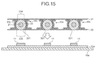
- FIG. 15 is a diagram to describe an assembly of the cable connection structure according to the modification of the fifth embodiment.
- the substrate 10a is connected to the cable 20c, as illustrated in FIG. 15 , the plurality of cables 20c which has been collectively held by the holding members 31 and 32 is placed on the substrate 10a, and each core wire 21 has contact with the first electrode 11.
- the first electrode 11 and the core wire 21 are fixed with the joining material and are electrically connected to each other.
- the joining member for example, a conductive joining member which is not illustrated such as solder, an ACF, and ACP is exemplified.
- the holding member 32 is fixed to the second electrode 12a via the joining material.
- the surface of the inner insulator 22 exposed through the exposed portion 234 has contact with the principal surface of the holding member 31, and the surface of the inner insulator 22 exposed through the exposed portion 235 is positioned in the hollow portion 321 (between divided parts of the holding member 32) and is connected to the substrate 10a in a state where the surface has contact with the second electrode 12a through the hollow portion 321. Accordingly, even when the holding members 31 and 32 are used, the attachment height of the cable 20c relative to the substrate 10a can be lower than that in a case where the exposed portions 234 and 235 are not formed in the shield 23c.
- the exposed portions 234 and 235 in which a part of the inner insulator 22 is exposed are formed by separating a part of the conductors, and the inner insulator 22 has contact with the holding member 31 through the exposed portion 234. Further, the inner insulator 22 has contact with the second electrode 12a through the exposed portion 235 and the hollow portion 321, and the conductors separated to form the exposed portions 234 and 235 respectively have contact with the holding members 31 and 32.
- the cable 20c is connected to the substrate 10a. Accordingly, the attachment height of the cable relative to the substrate can be lowered without microfabrication on the substrate.
- the plurality of cables 20c is attached to the substrate 10a in a state where the cables 20c are collectively held by the holding members 31 and 32. Therefore, it is easier to assemble the cable connection structure.
- the attachment height of the cable relative to the substrate can be further lower than that in the fifth embodiment.
- the holding member 31 may have contact with the second electrode 12a by turning the cable connection structure 1e upside down.
- the holding member 31 functions as the first holding member
- the holding member 32 functions as the second holding member.
- the attachment height of the cable relative to the substrate can be further lowered by using the holding member 32 instead of the holding member 31.
- the cable 20c is connected to the substrate 10a in a state where the surface of the inner insulator 22 in the exposed portion 235 has contact with the second electrode 12a.
- the above-mentioned effect can be obtained. Therefore, when at least a part of the surface of the inner insulator 22 in the exposed portion 235 is positioned in the hollow portion 321, a structure in which the surface of the inner insulator 22 does not have contact with the principal surface of the second electrode 12a can be applied.
- the exposed portion is formed by separating the conductors of the shield.
- the exposed portion may be formed by cutting off a part of the conductors.
- the cable connection structure according to the first to fifth embodiments is suitable for connecting a substrate of an imaging element of an endoscope and a coaxial cable, for example.
Landscapes
- Multi-Conductor Connections (AREA)
- Coupling Device And Connection With Printed Circuit (AREA)
- Cable Accessories (AREA)
Abstract
Description
- The present invention relates to a cable connection structure for connecting a cable to a substrate. Background
- A cable connection structure for connecting a substrate having an electronic component mounted thereon to a cable has been used in the related art according to a kind of a device such as a digital camera, a digital video camera, a portable telephone including an imaging function, and an endoscope device to observe inside of an organ of a subject.
- The endoscope device of the above devices has flexibility and includes a long and thin insertion tool which is inserted in a body of the subject and obtains an image signal regarding the inside of the organ and a signal processing unit which is connected to the insertion tool and performs signal processing to the image signal. In a distal end part of the insertion tool, an imaging unit which includes a substrate including an imaging element having a plurality of pixels mounted thereon is connected to a cable of which one end is connected to the signal processing unit. The image signal imaged by the imaging unit is transmitted to the signal processing unit via the cable.
- Regarding the endoscope device, the distal end part of the insertion tool has been required to be smaller in order to reduce a burden on the subject. According to this demand, the cable connection structure in the distal end part has been required to be small.
- In response to the above-mentioned demand, a technique has been known in which the attachment height of the cable relative to the substrate is lowered by forming a slit on an upper surface (surface to be connected) of the substrate and connecting the substrate to the cable by putting a part of the cable into the slit in a connection structure of a coaxial cable for connecting the cable to the substrate (See
Patent Literature 1, for example). - Patent Literature 1: Japanese Patent Application Laid-open No.
2001-68175 - However, the technique disclosed in
Patent Literature 1 requires advanced technique such as microfabrication of the substrate, it is difficult to form the slit. Therefore, there is a need to lower the attachment height of the cable without performing precision processing such as microfabrication on the substrate. - The present invention has been made in view of the foregoing, and an object of the invention is to provide a cable connection structure which can lower an attachment height of a cable relative to a substrate without microfabrication on the substrate.
- To solve the problem described above and to achieve the object, a cable connection structure according to the invention includes: one or a plurality of cables; and a substrate having an electrode thereon, the one or the plurality of cables being configured to be connected to the electrode. Each of the one or the plurality of cables includes: a core wire formed of a line-shaped conductive material; a tubular inner insulator which is formed of an insulator and covers an outer circumference of the core wire; a shield which extends along a longitudinal direction of the inner insulator and includes a plurality of conductors for covering an outer circumference of the inner insulator, and has an exposed portion for exposing the inner insulator; and an outer insulator formed of an insulator for covering an outer circumference of the shield. The shield including a region where the exposed portion is formed, the inner insulator, and the core wire are exposed in a stepped manner toward a distal end of each cable. The substrate includes: a first electrode configured to be electrically connected to the core wire; and a second electrode configured to be electrically connected to the shield.
- In the above-described cable connection structure according to the invention, the exposed portion is formed by separating a part of the exposed conductors of the shield.
- In the above-described cable connection structure according to the invention, the exposed portion is formed by cutting off a part of the exposed conductors of the shield.
- In the above-described cable connection structure according to the invention, the inner insulator has contact with the second electrode in a portion where the inner insulator is exposed through the exposed portion.
- In the above-described cable connection structure according to the invention, at least a part of a portion where the inner insulator is exposed through the exposed portion is positioned between divided parts of the second electrode.
- The cable connection structure according to the above-described invention further includes a substantially strip-shaped first holding member configured to collectively hold the plurality of cables and configured to be electrically connected to the second electrode. The shield is configured to be electrically connected to the second electrode via the first holding member.
- In the above-described cable connection structure according to the invention, the inner insulator has contact with a principal surface of the first holding member in a portion where the inner insulator is exposed through the exposed portion.
- In the above-described cable connection structure according to the invention, at least a part of a portion where the inner insulator is exposed through the exposed portion is positioned between divided parts of the first holding member.
- The cable connection structure according to the above-described invention further includes a substantially strip-shaped second holding member configured to collectively hold the plurality of cables. The plurality of cables is held and sandwiched by the first and second holding members.
- According to the present invention, it is possible to lower an attachment height of a cable relative to a substrate without microfabrication on the substrate. Brief Description of Drawings
-
FIG. 1 is a schematic diagram of an outline structure of a cable connection structure according to a first embodiment of the present invention. -
FIG. 2 is an A-A line sectional view of the cable connection structure illustrated inFIG. 1 . -
FIG. 3 is a schematic perspective view of a cable of the cable connection structure according to the first embodiment of the present invention. -
FIG. 4 is a B-B line sectional view of the cable connection structure illustrated inFIG. 1 . -
FIG. 5 is a schematic diagram of an outline structure of a cable connection structure according to a second embodiment of the present invention. -
FIG. 6 is a C-C line sectional view of the cable connection structure illustrated inFIG. 5 . -
FIG. 7 is a schematic diagram of an outline structure of a cable connection structure according to a third embodiment of the present invention. -
FIG. 8 is a D-D line sectional view of the cable connection structure illustrated inFIG. 7 . -
FIG. 9 is a schematic diagram of an outline structure of a cable connection structure according to a fourth embodiment of the present invention. -
FIG. 10 is an E-E line sectional view of the cable connection structure illustrated inFIG. 9 . -
FIG. 11 is a schematic diagram of an outline structure of a cable connection structure according to a fifth embodiment of the present invention. -
FIG. 12 is an F-F line sectional view of the cable connection structure illustrated inFIG. 11 . -
FIG. 13 is a diagram to describe an assembly of the cable connection structure according to the fifth embodiment of the present invention. -
FIG. 14 is a sectional view of an outline structure of a cable connection structure according to a modification of the fifth embodiment of the present invention. -
FIG. 15 is a diagram to describe an assembly of the cable connection structure according to the modification of the fifth embodiment of the present invention. - Embodiments of a cable connection structure according to the present invention will be described below with reference to the drawings. The present invention is not limited to the embodiments. The same reference signs are used to designate the same elements throughout the drawings.
-
FIG. 1 is a schematic diagram of an outline structure of a cable connection structure according to a first embodiment of the present invention.FIG. 2 is an A-A line sectional view of the cable connection structure illustrated inFIG. 1 .FIG. 3 is a schematic perspective view of a cable of the cable connection structure according to the first embodiment.FIG. 4 is a B-B line sectional view of the cable connection structure illustrated inFIG. 1 . Acable connection structure 1 according to the first embodiment includes asubstrate 10 having electronic components mounted thereon and acable 20 connected to thesubstrate 10. Thecable 20 will be described below while thecable 20 is assumed as a coaxial cable. - The
substrate 10 has a substantially plate shape, and an electric circuit, an electrode, and the like are formed on at least one principal surface. Also, on one principal surface of thesubstrate 10, afirst electrode 11 and asecond electrode 12 electrically connected to thecable 20 are formed. Here, thefirst electrode 11 is a connection electrode connected to thecable 20. Thesecond electrode 12 is a ground electrode having a substantially plate shape. - The
cable 20 includes: acore wire 21 formed of a line-shaped conductor (conductive material) made of copper and the like; a tubularinner insulator 22 which is formed of an insulator, covers the outer circumference of thecore wire 21, and exposes thecore wire 21 on a distal end side of theinner insulator 22; ashield 23 which extends along the longitudinal direction of theinner insulator 22 and includes a plurality of conductors for covering the outer circumference of theinner insulator 22; and anouter insulator 24 which is formed of an insulator for covering the outer circumference of theshield 23. Theinner insulator 22, theshield 23, and theouter insulator 24 are stripped in a stepped manner to form thecable 20 at the end part where thesubstrate 10 is connected. In thecable 20, by this stripping, theshield 23, theinner insulator 22, and thecore wire 21 are exposed in a stepped manner toward the distal end. The conductor of theshield 23 is made of the line-shaped conductive material. - Here, in a region of the
shield 23 exposed by the stripping, an exposedportion 231 is formed (refer toFIG. 3 ). The exposedportion 231 is formed by separating a part of the conductors to expose a part of theinner insulator 22. The conductors of theshield 23 are arranged while aligning the longitudinal directions with each other and arranged along the outer circumference of theinner insulator 22. A cross section of theshield 23 having a plane perpendicular to the longitudinal direction as a cut surface has a substantially annular shape. - In the
substrate 10 and thecable 20, thefirst electrode 11 and thecore wire 21 are fixed with a joining member and electrically connected to each other. As the joining member, a conductive joining member, which is not illustrated, such as solder, an anisotropic conductive film (ACF), and anisotropic conductive paste (ACP) is exemplified. - The
cable 20 is arranged such that the exposedportion 231 of theshield 23 faces to thesecond electrode 12. Thecable 20 is connected to thesubstrate 10 in a state where the surface of theinner insulator 22 in the exposedportion 231 has contact with thesecond electrode 12. The conductors separated to form the exposedportion 231 of theshield 23 are fixed on thesecond electrode 12 via the above-mentioned joining material. - Here, in the cross section illustrated in
FIG. 2 , a distance d1 between the principal surface of thesubstrate 10 and the end on the opposite side to the principal surface of thesubstrate 10 in theshield 23 is smaller than a value obtained by adding a diameter of a circle having contact with the outer edge of each conductor of theshield 23 to a board thickness of the second electrode 12 (distance perpendicular to the principal surface). The distance d1 corresponds to the length in the direction perpendicular to the principal surface of thesubstrate 10 and in the direction for passing through the center of the cable 20 (core wire 21). - In this way, the
substrate 10 is connected to thesecond electrode 12 in a state where the exposedportion 231 has been formed and theinner insulator 22 has had contact with thesecond electrode 12. Accordingly, the attachment height of thecable 20 relative to thesubstrate 10 can be lower than that in a case where the exposedportion 231 is not formed in theshield 23. Also, the attachment height of thecable 20 relative to thesubstrate 10 can be further lowered by reducing the thicknesses of thefirst electrode 11 and thesecond electrode 12. - According to the first embodiment, in the
shield 23, the exposedportion 231, in which a part of theinner insulator 22 is exposed, is formed by separating a part of the conductor, and theinner insulator 22 has contact with thesecond electrode 12 through the exposedportion 231. Also, thecable 20 is connected to thesubstrate 10 by contacting the conductor separated to form the exposedportion 231 with thesecond electrode 12. Therefore, the attachment height of the cable relative to the substrate can be lowered without microfabrication on the substrate. - Further, according to the first embodiment, a connecting position of the
core wire 21 to thefirst electrode 11 can be lowered by lowering the attachment height of the cable by contacting theinner insulator 22 with thesecond electrode 12 through the exposedportion 231. Accordingly, a connection state of thecore wire 21 to thefirst electrode 11 can be stabilized, and the reliability regarding the connection between thesubstrate 10 and thecable 20 can be improved. - Further, according to the first embodiment, by contacting the conductors separated to form the exposed
portion 231 with thesecond electrode 12, a shield function by theshield 23 can be secured, and the joining strength between thesubstrate 10 and thecable 20 can be improved. - Further, according to the first embodiment, in the
substrate 10, it is not necessary to form a slit where thecable 20 is put in, and manufacturing cost to form the slit can be made unnecessary. -
FIG. 5 is a schematic diagram of an outline structure of a cable connection structure according to a second embodiment of the present invention.FIG. 6 is a C-C line sectional view of the cable connection structure illustrated inFIG. 5 . The same reference signs are used to designate the same elements as the above-described elements. In acable connection structure 1a according to the second embodiment, a plurality ofcables 20 is connected to asubstrate 10a. - The
substrate 10a has a substantially plate shape, and an electric circuit, an electrode, and the like are formed on at least one principal surface. A plurality offirst electrodes 11 electrically connected to thecables 20 is formed on one principal surface of thesubstrate 10a. - On one principal surface of the
substrate 10a, asecond electrode 12a is formed which extends in an arrangement direction of the plurality ofcables 20 and is connected to theshields 23 of thecables 20. Thesecond electrode 12a is a shield connection electrode having a substantially plate shape and connected to eachshield 23. - As described above, the
cable 20 is arranged such that the exposedportions 231 of theshields 23 face to thesecond electrode 12a. Thecable 20 is connected to thesubstrate 10a in a state where the surfaces of theinner insulators 22 in the exposedportions 231 have contact with thesecond electrode 12a. The conductors separated to form the exposedportion 231 of theshield 23 are fixed on thesecond electrode 12a via the joining material. - Here, similarly to the first embodiment, a distance between the principal surface of the
substrate 10a and the end of theshield 23 becomes the distance d1 (refer toFIG. 2 ) smaller than a value obtained by adding a diameter of a circle having contact with the outer edge of each conductor of theshield 23 to a board thickness of thesecond electrode 12a. - In this way, the
substrate 10a is connected to thesecond electrode 12a in a state where the exposedportion 231 has been formed and theinner insulator 22 has had contact with thesecond electrode 12a. Accordingly, the attachment height of thecable 20 relative to thesubstrate 10a can be lower than that in a case where the exposedportion 231 is not formed in theshield 23. - According to the second embodiment, in the
shield 23, the exposedportion 231, in which a part of theinner insulator 22 is exposed, is formed by separating a part of the conductors, and theinner insulator 22 has contact with thesecond electrode 12a through the exposedportion 231. Also, the plurality ofcables 20 is connected to thesubstrate 10a by contacting the conductor separated to form the exposedportion 231 with thesecond electrode 12a. Therefore, the attachment height of the cable relative to the substrate can be lowered without microfabrication on the substrate. -
FIG. 7 is a schematic diagram of an outline structure of a cable connection structure according to a third embodiment of the present invention.FIG. 8 is a D-D line sectional view of the cable connection structure illustrated inFIG. 7 . The same reference signs are used to designate the same elements as the above-described elements. Acable connection structure 1b according to the third embodiment includes asubstrate 10b having an electronic component and the like mounted thereon and acable 20a connected to thesubstrate 10b. - The
substrate 10b has a substantially plate shape, and an electric circuit, an electrode, and the like are formed on at least one principal surface. On one principal surface of thesubstrate 10b, afirst electrode 11 electrically connected to thecable 20a and asecond electrode 12b connected to ashield 23a of thecable 20a are formed. Thesecond electrode 12b is a ground electrode. - The
cable 20a includes thecore wire 21, theinner insulator 22, theshield 23a which extends along the longitudinal direction of theinner insulator 22 and includes a plurality of conductors for covering the outer circumference of theinner insulator 22, anouter insulator 24 including an insulator for covering the outer circumference of theshield 23a. Theinner insulator 22, theshield 23a, and theouter insulator 24 are stripped in a stepped manner to form thecable 20a at the end part where thesubstrate 10b is connected. The cross section of theshield 23a perpendicular to the longitudinal direction of the conductor has a substantially annular shape. - In the
shield 23a, an exposedportion 232 which is formed by separating a part of the conductors is formed, and a part of theinner insulator 22 is exposed in the exposedportion 232. - The
cable 20a is fixed with the joining material at the distal end of thecore wire 21 and is electrically connected to thefirst electrode 11. - Here, the
second electrode 12b is divided in a direction substantially perpendicular to the arrangement direction of thefirst electrode 11 and thesecond electrode 12b (longitudinal direction ofsecond electrode 12b). By this division, ahollow portion 121 as a hollow space is formed in thesecond electrode 12b. The length (width) of thehollow portion 121 in the longitudinal direction is designed such that at least theinner insulator 22 of thecable 20a has contact with the principal surface of thesubstrate 10b so as to be housed in thehollow portion 121. Thesecond electrode 12b is electrically connected by wiring formed on the surface or in thesubstrate 10b. - The
cable 20a is arranged such that the exposedportion 232 of theshield 23a faces to the side of thesubstrate 10b. Thecable 20a is connected to thesubstrate 10b in a state where the surface of theinner insulator 22 in the exposedportion 232 has been positioned in the hollow portion 121 (between the divided parts of thesecond electrode 12b) and has had contact with the principal surface of thesubstrate 10b via thehollow portion 121. The conductors separated to form the exposedportion 232 of theshield 23a are fixed on thesecond electrode 12b via the joining material. - Here, as illustrated in
FIG. 8 , a distance d2 between the principal surface of thesubstrate 10b to the end of theshield 23a is smaller than a value obtained by adding a diameter of a circle having contact with the outer edge of each conductor of theshield 23a to a board thickness of thesecond electrode 12b (distance perpendicular to the principal surface). The distance d2 corresponds to the length in the direction perpendicular to the principal surface of thesubstrate 10b and in the direction for passing through the center of thecable 20a (core wire 21). - In this way, the
substrate 10b is connected to theinner insulator 22 in a state where the exposedportion 232 has been formed and theinner insulator 22 has had contact with the principal surface of thesubstrate 10b. Accordingly, the attachment height of thecable 20a relative to thesubstrate 10b can be lower than that in a case where the exposedportion 232 is not formed in theshield 23a. - According to the third embodiment, in the
shield 23a, the exposedportion 232 in which a part of theinner insulator 22 is exposed is formed by separating a part of the conductors, and theinner insulator 22 has contact with the principal surface of thesubstrate 10b through the exposedportion 232. Also, the plurality ofcables 20a is connected to thesubstrate 10b by contacting the conductors separated to form the exposedportion 232 with thesecond electrode 12b. Therefore, the attachment height of the cable relative to the substrate can be lowered without microfabrication on the substrate. - Further, in the third embodiment, since the
inner insulator 22 is put into a position contacting with the principal surface of thesubstrate 10b, the distance d2 is smaller than the distance d1. Accordingly, relative to the first and second embodiments, the attachment height of the cable relative to the substrate can be further lowered. -
FIG. 9 is a schematic diagram of an outline structure of a cable connection structure according to a fourth embodiment of the present invention.FIG. 10 is an E-E line sectional view of the cable connection structure illustrated inFIG. 9 . The same reference signs are used to designate the same elements as the above-described elements. In acable connection structure 1c according to the fourth embodiment, the plurality ofcables 20a is connected to asubstrate 10c. - The
substrate 10c has a substantially plate shape, and an electric circuit, an electrode, and the like are formed on at least one principal surface. A plurality offirst electrodes 11 electrically connected to thecables 20a is formed on one principal surface of thesubstrate 10c. On one of the principal surface of thesubstrate 10c, asecond electrode 12c is formed which extends in an arrangement direction of the plurality ofcables 20a and is connected to theshields 23a of thecables 20a. Thesecond electrode 12c is a ground electrode connected to eachshield 23a. - Here, the
second electrode 12c is divided in the longitudinal direction according to the number of the arrangedcables 20a. In thesecond electrode 12c, a plurality ofhollow portions 122 as a hollow space is formed (according to the number of the arrangedcables 20a) by this division. The length of thehollow portion 122 in the longitudinal direction is designed such that at least theinner insulator 22 of thecable 20a has contact with the principal surface of thesubstrate 10c so as to be housed in thehollow portion 122. Thesecond electrode 12c is electrically connected by wiring formed on the surface or in thesubstrate 10c. - The
cable 20a is arranged such that the exposedportion 232 of theshield 23a faces to the side of thesubstrate 10c. Thecable 20a is connected to thesubstrate 10c in a state where the surface of theinner insulator 22 in the exposedportion 232 has been positioned in the hollow portion 122 (between divided parts of thesecond electrode 12c) and has had contact with the principal surface of thesubstrate 10c via thehollow portion 122. The conductors separated to form the exposedportion 232 of theshield 23a are fixed on thesecond electrode 12c via the joining material. - Here, similarly to the third embodiment, a distance between the principal surface of the
substrate 10c and the end of theshield 23a becomes the distance d2 (refer toFIG. 8 ) smaller than a value obtained by adding a diameter of a circle having contact with the outer edge of each conductor of theshield 23a to a board thickness of thesecond electrode 12c. - In this way, the
substrate 10c is connected to theinner insulator 22 in a state where the exposedportion 232 has been formed and theinner insulator 22 has had contact with the principal surface of thesubstrate 10c. Accordingly, the attachment height of thecable 20a relative to thesubstrate 10c can be lower than that in a case where the exposedportion 232 is not formed in theshield 23a. - According to the fourth embodiment, in the
shield 23a, the exposedportion 232 in which a part of theinner insulator 22 is exposed is formed by separating a part of the conductors, and theinner insulator 22 has contact with the principal surface of thesubstrate 10c through the exposedportion 232. Also, the plurality ofcables 20a is connected to thesubstrate 10c by contacting the conductors separated to form the exposedportion 232 with thesecond electrode 12c. Therefore, the attachment height of the cable relative to the substrate can be lowered without microfabrication on the substrate. - In the third and fourth embodiments, the
inner insulator 22 is connected to thesubstrate 10c in a state where the surface of theinner insulator 22 in the exposedportion 232 has contact with the principal surface of thesubstrate hollow portion 121 or 122 (between divided parts of thesecond electrode inner insulator 22 in the exposedportion 232 is positioned in thehollow portions inner insulator 22 does not have contact with the principal surface of thesubstrates -
FIG. 11 is a schematic diagram of an outline structure of a cable connection structure according to a fifth embodiment of the present invention.FIG. 12 is an F-F line sectional view of the cable connection structure illustrated inFIG. 11 . Acable connection structure 1d according to the fifth embodiment includes thesubstrate 10a, a plurality ofcables 20b connected to thesubstrate 10a, and a holding member 30 (first holding member) and a holding member 31 (second holding member) for collectively holding the plurality ofcables 20b. - The
substrate 10a has a substantially plate shape, and an electric circuit, an electrode, and the like are formed on at least one principal surface. A plurality offirst electrodes 11 electrically connected to thecables 20b is formed on one principal surface of thesubstrate 10a. On one principal surface of thesubstrate 10a, asecond electrode 12a is formed which extends in the arrangement direction of the plurality ofcables 20b and is connected to the holdingmember 30. - The
cable 20b includes: thecore wire 21; theinner insulator 22; ashield 23b which extends along the longitudinal direction of theinner insulator 22 and includes a plurality of conductors for covering the outer circumference of theinner insulator 22; and anouter insulator 24 formed of an insulator for covering the outer circumference of theshield 23b. Theinner insulator 22, theshield 23b, and theouter insulator 24 are stripped in a stepped manner to form thecable 20b at the end part where thesubstrate 10a is connected. The cross section of theshield 23b perpendicular to the longitudinal direction of the conductor has a substantially annular shape. - The holding
members members cables 20b by being connected to a part of the conductors of eachshield 23b via a joining material and the like. The holdingmembers - Here, in the
shield 23b, exposedportions inner insulator 22 is exposed in the exposedportions portions core wire 21. - In the
cable 20b, the exposedportions shield 23b are respectively arranged opposite to the principal surfaces of the holdingmembers cable 20b is connected to thesubstrate 10a in a state where the surfaces of theinner insulator 22 in the exposedportions members portions shield 23 are respectively fixed to the holdingmembers -
FIG. 13 is a diagram to describe an assembly of the cable connection structure according to the fifth embodiment. When thesubstrate 10a is connected to thecable 20b, as illustrated inFIG. 13 , the plurality ofcables 20b which has been collectively held by the holdingmember substrate 10a, and eachcore wire 21 has contact with thefirst electrode 11. - After that, the
first electrode 11 and thecore wire 21 are fixed with the joining material and are electrically connected to each other. As the joining member, for example, a conductive joining member which is not illustrated such as solder, an ACF, and ACP is exemplified. Also, the holdingmember 30 is fixed to thesecond electrode 12a via the joining material. - In this way, the exposed
portions inner insulator 22 is contacted with the principal surfaces of the holdingmembers substrate 10a. Accordingly, even when the holdingmembers cable 20b relative to thesubstrate 10a can be lower than that in a case where the exposedportions shield 23b. - According to the fifth embodiment, in the
shield 23b, the exposedportions inner insulator 22 is exposed are formed by separating a part of the conductors, and theinner insulator 22 has contact with the holdingmembers portions cable 20b is connected to thesubstrate 10a by contacting the conductors separated to form the exposedportions members - Further, according to the fifth embodiment, the plurality of
cables 20b is attached to thesubstrate 10a in a state where thecables 20b are collectively held by the holdingmembers - In the fifth embodiment, the plurality of
cables 20b is collectively held by the holdingmembers cables 20b may be held by one of the holding members. For example, when only the holdingmember 30 is used, a part of theinner insulator 22 exposed to outside by the exposedportion 233 has contact with thesecond electrode 12a, and the conductors of theshield 23b are fixed to thesecond electrode 12a. -
FIG. 14 is a sectional view of an outline structure of a cable connection structure according to a modification of the fifth embodiment of the present invention. Acable connection structure 1e according to the modification of the fifth embodiment includes a holding member 32 (first holding member) and acable 20c instead of the holdingmember 30 and thecable 20b according to the fifth embodiment. The holdingmember 32 includes, for example, a plurality of strip-shapedmembers first electrodes 11. In the holdingmember 32, the strip-shapedmembers members member 31. - The strip-shaped
members 32a are arranged so as to be positioned on both sides of the holdingmember 32 in the longitudinal direction of the holdingmember 32. Also, the strip-shapedmember 32b is arranged between the strip-shapedmembers 32a and arranged according to the arrangement intervals of the plurality ofcables 20c. It is preferable that the interval between the strip-shapedmembers inner insulator 22 can be held in a state where the outer circumference of theinner insulator 22 is positioned on the plane for passing through the principal surfaces of the strip-shapedmembers - The
cable 20c includes thecore wire 21, theinner insulator 22, ashield 23c which extends along the longitudinal direction of theinner insulator 22 and includes a plurality of conductors for covering the outer circumference of theinner insulator 22, and anouter insulator 24 formed of an insulator for covering the outer circumference of theshield 23c. Theinner insulator 22, theshield 23c, and theouter insulator 24 are stripped in a stepped manner to form thecable 20c at the end part where thesubstrate 10a is connected. - In the
shield 23c, an exposedportions inner insulator 22 is exposed in the exposedportions - Here, in the holding
member 32,hollow portions 321 are formed by arranging a space between the strip-shapedmember 32a and the strip-shapedmember 32b and a space between the strip-shapedmembers 32b at predetermined intervals. The length of thehollow portion 321 in the longitudinal direction is designed as a width such that at least the outer surface of theinner insulator 22 of thecable 20c has contact with a plane for passing through the principal surfaces of the strip-shapedmembers inner insulator 22 can be housed in thehollow portion 321. - The
cable 20c is arranged such that the exposedportion 234 of theshield 23c faces to the side of the holdingmember 31 and the exposedportion 235 faces to thehollow portion 321. On the other hand, thecable 20c is connected to thesubstrate 10a in a state where the surface of theinner insulator 22 housed in thehollow portion 321 and the holdingmember 32 have contact with thesecond electrode 12a. The conductors separated to form the exposedportions shield 23c are fixed to the holding member 32 (strip-shapedmembers -
FIG. 15 is a diagram to describe an assembly of the cable connection structure according to the modification of the fifth embodiment. When thesubstrate 10a is connected to thecable 20c, as illustrated inFIG. 15 , the plurality ofcables 20c which has been collectively held by the holdingmembers substrate 10a, and eachcore wire 21 has contact with thefirst electrode 11. - After that, the
first electrode 11 and thecore wire 21 are fixed with the joining material and are electrically connected to each other. As the joining member, for example, a conductive joining member which is not illustrated such as solder, an ACF, and ACP is exemplified. Also, the holdingmember 32 is fixed to thesecond electrode 12a via the joining material. - In this way, the surface of the
inner insulator 22 exposed through the exposedportion 234 has contact with the principal surface of the holdingmember 31, and the surface of theinner insulator 22 exposed through the exposedportion 235 is positioned in the hollow portion 321 (between divided parts of the holding member 32) and is connected to thesubstrate 10a in a state where the surface has contact with thesecond electrode 12a through thehollow portion 321. Accordingly, even when the holdingmembers cable 20c relative to thesubstrate 10a can be lower than that in a case where the exposedportions shield 23c. - According to the modification of the fifth embodiment, in the
shield 23c, the exposedportions inner insulator 22 is exposed are formed by separating a part of the conductors, and theinner insulator 22 has contact with the holdingmember 31 through the exposedportion 234. Further, theinner insulator 22 has contact with thesecond electrode 12a through the exposedportion 235 and thehollow portion 321, and the conductors separated to form the exposedportions members cable 20c is connected to thesubstrate 10a. Accordingly, the attachment height of the cable relative to the substrate can be lowered without microfabrication on the substrate. - Further, according to the modification of the fifth embodiment, the plurality of
cables 20c is attached to thesubstrate 10a in a state where thecables 20c are collectively held by the holdingmembers - Further, in the modification of the fifth embodiment, since the
inner insulator 22 is put into a position contacting with the principal surface of thesecond electrode 12a, the attachment height of the cable relative to the substrate can be further lower than that in the fifth embodiment. - In the modification of the fifth embodiment, the holding
member 31 may have contact with thesecond electrode 12a by turning thecable connection structure 1e upside down. In this case, the holdingmember 31 functions as the first holding member, and the holdingmember 32 functions as the second holding member. Also, the attachment height of the cable relative to the substrate can be further lowered by using the holdingmember 32 instead of the holdingmember 31. - Further, in the modification of the fifth embodiment, the
cable 20c is connected to thesubstrate 10a in a state where the surface of theinner insulator 22 in the exposedportion 235 has contact with thesecond electrode 12a. However, when the surface is positioned in thehollow portion 321, the above-mentioned effect can be obtained. Therefore, when at least a part of the surface of theinner insulator 22 in the exposedportion 235 is positioned in thehollow portion 321, a structure in which the surface of theinner insulator 22 does not have contact with the principal surface of thesecond electrode 12a can be applied. - In the first to fifth embodiments, the exposed portion is formed by separating the conductors of the shield. However, the exposed portion may be formed by cutting off a part of the conductors.
- The cable connection structure according to the first to fifth embodiments is suitable for connecting a substrate of an imaging element of an endoscope and a coaxial cable, for example.
-
- 1, 1a, 1b, 1c, 1d, 1e Cable Connection Structure
- 10, 10a, 10b, 10c substrate
- 11 first electrode
- 12, 12a, 12b, 12c second electrode
- 20, 20a, 20b, 20c cable
- 21 core wire
- 22 inner insulator
- 23, 23a, 23b, 23c shield
- 24 outer insulator
- 30, 31, 32 holding member
- 121, 122, 321 hollow portion
- 231, 232, 233, 234, 235 exposed portion
Claims (9)
- A cable connection structure comprising:one or a plurality of cables; anda substrate having an electrode thereon, the one or the plurality of cables being configured to be connected to the electrode, whereineach of the one or the plurality of cables comprises:a core wire formed of a line-shaped conductive material;a tubular inner insulator which is formed of an insulator and covers an outer circumference of the core wire;a shield which extends along a longitudinal direction of the inner insulator and includes a plurality of conductors for covering an outer circumference of the inner insulator, and has an exposed portion for exposing the inner insulator; andan outer insulator formed of an insulator for covering an outer circumference of the shield, whereinthe shield including a region where the exposed portion is formed, the inner insulator, and the core wire are exposed in a stepped manner toward a distal end of each cable, andthe substrate comprises:a first electrode configured to be electrically connected to the core wire; anda second electrode configured to be electrically connected to the shield.
- The cable connection structure according to claim 1, wherein the exposed portion is formed by separating a part of the exposed conductors of the shield.
- The cable connection structure according to claim 1, wherein the exposed portion is formed by cutting off a part of the exposed conductors of the shield.
- The cable connection structure according to any one of claims 1 to 3, wherein
the inner insulator has contact with the second electrode in a portion where the inner insulator is exposed through the exposed portion. - The cable connection structure according to any one of claims 1 to 3, wherein
at least a part of a portion where the inner insulator is exposed through the exposed portion is positioned between divided parts of the second electrode. - The cable connection structure according to any one of claims 1 to 3, further comprising a substantially strip-shaped first holding member configured to collectively hold the plurality of cables and configured to be electrically connected to the second electrode, wherein
the shield is configured to be electrically connected to the second electrode via the first holding member. - The cable connection structure according to claim 6, wherein the inner insulator has contact with a principal surface of the first holding member in a portion where the inner insulator is exposed through the exposed portion.
- The cable connection structure according to claim 6, wherein at least a part of a portion where the inner insulator is exposed through the exposed portion is positioned between divided parts of the first holding member.
- The cable connection structure according to any one of claims 6 to 8, further comprising a substantially strip-shaped second holding member configured to collectively hold the plurality of cables, wherein
the plurality of cables is held and sandwiched by the first and second holding members.
Applications Claiming Priority (2)
| Application Number | Priority Date | Filing Date | Title |
|---|---|---|---|
| JP2013122004 | 2013-06-10 | ||
| PCT/JP2014/064964 WO2014199897A1 (en) | 2013-06-10 | 2014-06-05 | Cable connection structure |
Publications (3)
| Publication Number | Publication Date |
|---|---|
| EP3010089A1 true EP3010089A1 (en) | 2016-04-20 |
| EP3010089A4 EP3010089A4 (en) | 2017-03-22 |
| EP3010089B1 EP3010089B1 (en) | 2018-07-18 |
Family
ID=52022193
Family Applications (1)
| Application Number | Title | Priority Date | Filing Date |
|---|---|---|---|
| EP14810848.3A Active EP3010089B1 (en) | 2013-06-10 | 2014-06-05 | Cable connection structure |
Country Status (5)
| Country | Link |
|---|---|
| US (1) | US9774151B2 (en) |
| EP (1) | EP3010089B1 (en) |
| JP (1) | JP6257618B2 (en) |
| CN (1) | CN105284008B (en) |
| WO (1) | WO2014199897A1 (en) |
Families Citing this family (6)
| Publication number | Priority date | Publication date | Assignee | Title |
|---|---|---|---|---|
| JP6519462B2 (en) * | 2015-12-10 | 2019-05-29 | 住友電気工業株式会社 | Cable assembly |
| WO2017122335A1 (en) * | 2016-01-14 | 2017-07-20 | オリンパス株式会社 | Imaging device, endoscope, and method for producing imaging device |
| DE202016101128U1 (en) | 2016-03-02 | 2016-03-11 | Amphenol-Tuchel Electronics Gmbh | Screen connection element for a printed circuit board |
| US11217918B2 (en) * | 2016-07-28 | 2022-01-04 | 3M Innovative Properties Company | Electrical cable |
| JP6840579B2 (en) * | 2017-03-13 | 2021-03-10 | 日本航空電子工業株式会社 | connector |
| WO2020012566A1 (en) * | 2018-07-10 | 2020-01-16 | オリンパス株式会社 | Cable connection structure, endoscope and method for manufacturing cable connection structure |
Family Cites Families (15)
| Publication number | Priority date | Publication date | Assignee | Title |
|---|---|---|---|---|
| JPS63231887A (en) * | 1987-03-18 | 1988-09-27 | 株式会社東芝 | Attachment structure of coaxial cable |
| JP2544247Y2 (en) * | 1990-11-14 | 1997-08-13 | 株式会社潤工社 | Coaxial cable connection structure |
| JP3111655B2 (en) * | 1992-07-08 | 2000-11-27 | 富士通株式会社 | Connection method between multi-pole connector for coaxial cable and its coaxial cable |
| JP4151168B2 (en) | 1999-08-30 | 2008-09-17 | ミツミ電機株式会社 | Antenna device |
| JP3976473B2 (en) * | 2000-05-09 | 2007-09-19 | 日本電気株式会社 | High frequency circuit and module and communication device using the same |
| JP2003168499A (en) * | 2001-11-29 | 2003-06-13 | Hitachi Kokusai Electric Inc | Coaxial cable connection structure |
| US6734374B2 (en) * | 2002-05-30 | 2004-05-11 | Hon Hai Precision Ind. Co., Ltd. | Micro-coaxial cable assembly and method for making the same |
| US6857898B2 (en) * | 2002-07-25 | 2005-02-22 | Tektronix, Inc. | Apparatus and method for low-profile mounting of a multi-conductor coaxial cable launch to an electronic circuit board |
| JP4889243B2 (en) * | 2005-06-09 | 2012-03-07 | モレックス インコーポレイテド | Connector device |
| JP4935252B2 (en) * | 2005-12-21 | 2012-05-23 | 住友電気工業株式会社 | Multi-fiber cable connection structure, multi-core cable, and method for manufacturing multi-core cable connection structure |
| US7498523B2 (en) * | 2006-02-06 | 2009-03-03 | Efficere Inc. | Direct wire attach |
| JP4848878B2 (en) * | 2006-07-27 | 2011-12-28 | 住友電気工業株式会社 | Coaxial cable connection structure, coaxial cable, and method of manufacturing coaxial cable connection structure |
| JP4983687B2 (en) * | 2007-03-27 | 2012-07-25 | 住友電気工業株式会社 | Shield electrical connection method |
| JP5365389B2 (en) * | 2009-07-21 | 2013-12-11 | 住友電気工業株式会社 | Coaxial cable harness |
| JP5631618B2 (en) * | 2010-04-08 | 2014-11-26 | オリンパス株式会社 | Cable connection structure |
-
2014
- 2014-06-05 WO PCT/JP2014/064964 patent/WO2014199897A1/en not_active Ceased
- 2014-06-05 JP JP2015522741A patent/JP6257618B2/en active Active
- 2014-06-05 CN CN201480032879.6A patent/CN105284008B/en active Active
- 2014-06-05 EP EP14810848.3A patent/EP3010089B1/en active Active
-
2015
- 2015-12-09 US US14/963,403 patent/US9774151B2/en active Active
Non-Patent Citations (1)
| Title |
|---|
| See references of WO2014199897A1 * |
Also Published As
| Publication number | Publication date |
|---|---|
| JPWO2014199897A1 (en) | 2017-02-23 |
| JP6257618B2 (en) | 2018-01-10 |
| CN105284008A (en) | 2016-01-27 |
| EP3010089A4 (en) | 2017-03-22 |
| WO2014199897A1 (en) | 2014-12-18 |
| CN105284008B (en) | 2019-04-12 |
| EP3010089B1 (en) | 2018-07-18 |
| US9774151B2 (en) | 2017-09-26 |
| US20160093991A1 (en) | 2016-03-31 |
Similar Documents
| Publication | Publication Date | Title |
|---|---|---|
| EP3010089B1 (en) | Cable connection structure | |
| TWI650905B (en) | Cable connection structure and cable connector | |
| CN106171049B (en) | Electronic equipment | |
| JP5904107B2 (en) | Cable connector, cable assembly, and method of manufacturing cable assembly | |
| JP2009076375A (en) | Multi-core cable connector | |
| US9124026B2 (en) | Cable assembly, electronic circuit module, and imaging apparatus | |
| CN107112082A (en) | The manufacture method of installation cable and installation cable | |
| KR102733474B1 (en) | Flexible flat cable and method for manufacturing the same | |
| US10211551B2 (en) | Electronic circuit module | |
| TW201324548A (en) | Flexible flat cable | |
| JP4910721B2 (en) | Connection structure of multi-core cable, multi-core cable with connector and multi-core cable | |
| CN101329929A (en) | Cable harnesses and cable harnesses with connectors | |
| JP2005063878A (en) | Connection structure | |
| JP2014089902A (en) | Cable connection body and cable connection method | |
| JP4470935B2 (en) | Multi-core coaxial cable and manufacturing method thereof | |
| US10888217B2 (en) | Imaging module applicable to head-swing endoscope | |
| JP6638735B2 (en) | Multi-core cable with connector and method of manufacturing the same | |
| JP6615447B2 (en) | Electrical connector | |
| JP6083397B2 (en) | Method and apparatus for connecting differential signal transmission cable to substrate | |
| JP2002184485A (en) | Multi-core wiring member with connection body and method of manufacturing the same | |
| KR101749803B1 (en) | Wiring member | |
| EP3449801A1 (en) | Imaging module and imaging-module-attached catheter | |
| JP2018147609A (en) | Cable alignment tool | |
| JP2013143276A (en) | Small-diameter coaxial cable harness with connection member |
Legal Events
| Date | Code | Title | Description |
|---|---|---|---|
| PUAI | Public reference made under article 153(3) epc to a published international application that has entered the european phase |
Free format text: ORIGINAL CODE: 0009012 |
|
| 17P | Request for examination filed |
Effective date: 20151231 |
|
| AK | Designated contracting states |
Kind code of ref document: A1 Designated state(s): AL AT BE BG CH CY CZ DE DK EE ES FI FR GB GR HR HU IE IS IT LI LT LU LV MC MK MT NL NO PL PT RO RS SE SI SK SM TR |
|
| AX | Request for extension of the european patent |
Extension state: BA ME |
|
| DAX | Request for extension of the european patent (deleted) | ||
| RAP1 | Party data changed (applicant data changed or rights of an application transferred) |
Owner name: OLYMPUS CORPORATION |
|
| A4 | Supplementary search report drawn up and despatched |
Effective date: 20170221 |
|
| RIC1 | Information provided on ipc code assigned before grant |
Ipc: H01R 12/53 20110101ALI20170215BHEP Ipc: H01R 9/05 20060101AFI20170215BHEP Ipc: H01R 24/38 20110101ALI20170215BHEP |
|
| GRAP | Despatch of communication of intention to grant a patent |
Free format text: ORIGINAL CODE: EPIDOSNIGR1 |
|
| STAA | Information on the status of an ep patent application or granted ep patent |
Free format text: STATUS: GRANT OF PATENT IS INTENDED |
|
| INTG | Intention to grant announced |
Effective date: 20180118 |
|
| GRAS | Grant fee paid |
Free format text: ORIGINAL CODE: EPIDOSNIGR3 |
|
| GRAA | (expected) grant |
Free format text: ORIGINAL CODE: 0009210 |
|
| STAA | Information on the status of an ep patent application or granted ep patent |
Free format text: STATUS: THE PATENT HAS BEEN GRANTED |
|
| RIN1 | Information on inventor provided before grant (corrected) |
Inventor name: KOBAYASHI, KEIICHI Inventor name: YAMADA, JUNYA |
|
| AK | Designated contracting states |
Kind code of ref document: B1 Designated state(s): AL AT BE BG CH CY CZ DE DK EE ES FI FR GB GR HR HU IE IS IT LI LT LU LV MC MK MT NL NO PL PT RO RS SE SI SK SM TR |
|
| REG | Reference to a national code |
Ref country code: GB Ref legal event code: FG4D |
|
| REG | Reference to a national code |
Ref country code: CH Ref legal event code: EP |
|
| REG | Reference to a national code |
Ref country code: IE Ref legal event code: FG4D |
|
| REG | Reference to a national code |
Ref country code: AT Ref legal event code: REF Ref document number: 1020357 Country of ref document: AT Kind code of ref document: T Effective date: 20180815 |
|
| REG | Reference to a national code |
Ref country code: DE Ref legal event code: R096 Ref document number: 602014028828 Country of ref document: DE |
|
| REG | Reference to a national code |
Ref country code: NL Ref legal event code: MP Effective date: 20180718 |
|
| REG | Reference to a national code |
Ref country code: LT Ref legal event code: MG4D |
|
| REG | Reference to a national code |
Ref country code: AT Ref legal event code: MK05 Ref document number: 1020357 Country of ref document: AT Kind code of ref document: T Effective date: 20180718 |
|
| PG25 | Lapsed in a contracting state [announced via postgrant information from national office to epo] |
Ref country code: NL Free format text: LAPSE BECAUSE OF FAILURE TO SUBMIT A TRANSLATION OF THE DESCRIPTION OR TO PAY THE FEE WITHIN THE PRESCRIBED TIME-LIMIT Effective date: 20180718 |
|
| PG25 | Lapsed in a contracting state [announced via postgrant information from national office to epo] |
Ref country code: NO Free format text: LAPSE BECAUSE OF FAILURE TO SUBMIT A TRANSLATION OF THE DESCRIPTION OR TO PAY THE FEE WITHIN THE PRESCRIBED TIME-LIMIT Effective date: 20181018 Ref country code: SE Free format text: LAPSE BECAUSE OF FAILURE TO SUBMIT A TRANSLATION OF THE DESCRIPTION OR TO PAY THE FEE WITHIN THE PRESCRIBED TIME-LIMIT Effective date: 20180718 Ref country code: GR Free format text: LAPSE BECAUSE OF FAILURE TO SUBMIT A TRANSLATION OF THE DESCRIPTION OR TO PAY THE FEE WITHIN THE PRESCRIBED TIME-LIMIT Effective date: 20181019 Ref country code: RS Free format text: LAPSE BECAUSE OF FAILURE TO SUBMIT A TRANSLATION OF THE DESCRIPTION OR TO PAY THE FEE WITHIN THE PRESCRIBED TIME-LIMIT Effective date: 20180718 Ref country code: FI Free format text: LAPSE BECAUSE OF FAILURE TO SUBMIT A TRANSLATION OF THE DESCRIPTION OR TO PAY THE FEE WITHIN THE PRESCRIBED TIME-LIMIT Effective date: 20180718 Ref country code: PL Free format text: LAPSE BECAUSE OF FAILURE TO SUBMIT A TRANSLATION OF THE DESCRIPTION OR TO PAY THE FEE WITHIN THE PRESCRIBED TIME-LIMIT Effective date: 20180718 Ref country code: IS Free format text: LAPSE BECAUSE OF FAILURE TO SUBMIT A TRANSLATION OF THE DESCRIPTION OR TO PAY THE FEE WITHIN THE PRESCRIBED TIME-LIMIT Effective date: 20181118 Ref country code: AT Free format text: LAPSE BECAUSE OF FAILURE TO SUBMIT A TRANSLATION OF THE DESCRIPTION OR TO PAY THE FEE WITHIN THE PRESCRIBED TIME-LIMIT Effective date: 20180718 Ref country code: LT Free format text: LAPSE BECAUSE OF FAILURE TO SUBMIT A TRANSLATION OF THE DESCRIPTION OR TO PAY THE FEE WITHIN THE PRESCRIBED TIME-LIMIT Effective date: 20180718 Ref country code: BG Free format text: LAPSE BECAUSE OF FAILURE TO SUBMIT A TRANSLATION OF THE DESCRIPTION OR TO PAY THE FEE WITHIN THE PRESCRIBED TIME-LIMIT Effective date: 20181018 |
|
| PG25 | Lapsed in a contracting state [announced via postgrant information from national office to epo] |
Ref country code: AL Free format text: LAPSE BECAUSE OF FAILURE TO SUBMIT A TRANSLATION OF THE DESCRIPTION OR TO PAY THE FEE WITHIN THE PRESCRIBED TIME-LIMIT Effective date: 20180718 Ref country code: LV Free format text: LAPSE BECAUSE OF FAILURE TO SUBMIT A TRANSLATION OF THE DESCRIPTION OR TO PAY THE FEE WITHIN THE PRESCRIBED TIME-LIMIT Effective date: 20180718 Ref country code: HR Free format text: LAPSE BECAUSE OF FAILURE TO SUBMIT A TRANSLATION OF THE DESCRIPTION OR TO PAY THE FEE WITHIN THE PRESCRIBED TIME-LIMIT Effective date: 20180718 |
|
| REG | Reference to a national code |
Ref country code: DE Ref legal event code: R097 Ref document number: 602014028828 Country of ref document: DE |
|
| PG25 | Lapsed in a contracting state [announced via postgrant information from national office to epo] |
Ref country code: EE Free format text: LAPSE BECAUSE OF FAILURE TO SUBMIT A TRANSLATION OF THE DESCRIPTION OR TO PAY THE FEE WITHIN THE PRESCRIBED TIME-LIMIT Effective date: 20180718 Ref country code: RO Free format text: LAPSE BECAUSE OF FAILURE TO SUBMIT A TRANSLATION OF THE DESCRIPTION OR TO PAY THE FEE WITHIN THE PRESCRIBED TIME-LIMIT Effective date: 20180718 Ref country code: CZ Free format text: LAPSE BECAUSE OF FAILURE TO SUBMIT A TRANSLATION OF THE DESCRIPTION OR TO PAY THE FEE WITHIN THE PRESCRIBED TIME-LIMIT Effective date: 20180718 Ref country code: ES Free format text: LAPSE BECAUSE OF FAILURE TO SUBMIT A TRANSLATION OF THE DESCRIPTION OR TO PAY THE FEE WITHIN THE PRESCRIBED TIME-LIMIT Effective date: 20180718 Ref country code: IT Free format text: LAPSE BECAUSE OF FAILURE TO SUBMIT A TRANSLATION OF THE DESCRIPTION OR TO PAY THE FEE WITHIN THE PRESCRIBED TIME-LIMIT Effective date: 20180718 |
|
| PLBE | No opposition filed within time limit |
Free format text: ORIGINAL CODE: 0009261 |
|
| STAA | Information on the status of an ep patent application or granted ep patent |
Free format text: STATUS: NO OPPOSITION FILED WITHIN TIME LIMIT |
|
| PG25 | Lapsed in a contracting state [announced via postgrant information from national office to epo] |
Ref country code: SK Free format text: LAPSE BECAUSE OF FAILURE TO SUBMIT A TRANSLATION OF THE DESCRIPTION OR TO PAY THE FEE WITHIN THE PRESCRIBED TIME-LIMIT Effective date: 20180718 Ref country code: SM Free format text: LAPSE BECAUSE OF FAILURE TO SUBMIT A TRANSLATION OF THE DESCRIPTION OR TO PAY THE FEE WITHIN THE PRESCRIBED TIME-LIMIT Effective date: 20180718 Ref country code: DK Free format text: LAPSE BECAUSE OF FAILURE TO SUBMIT A TRANSLATION OF THE DESCRIPTION OR TO PAY THE FEE WITHIN THE PRESCRIBED TIME-LIMIT Effective date: 20180718 |
|
| 26N | No opposition filed |
Effective date: 20190423 |
|
| PG25 | Lapsed in a contracting state [announced via postgrant information from national office to epo] |
Ref country code: SI Free format text: LAPSE BECAUSE OF FAILURE TO SUBMIT A TRANSLATION OF THE DESCRIPTION OR TO PAY THE FEE WITHIN THE PRESCRIBED TIME-LIMIT Effective date: 20180718 |
|
| PG25 | Lapsed in a contracting state [announced via postgrant information from national office to epo] |
Ref country code: MC Free format text: LAPSE BECAUSE OF FAILURE TO SUBMIT A TRANSLATION OF THE DESCRIPTION OR TO PAY THE FEE WITHIN THE PRESCRIBED TIME-LIMIT Effective date: 20180718 |
|
| REG | Reference to a national code |
Ref country code: CH Ref legal event code: PL |
|
| GBPC | Gb: european patent ceased through non-payment of renewal fee |
Effective date: 20190605 |
|
| REG | Reference to a national code |
Ref country code: BE Ref legal event code: MM Effective date: 20190630 |
|
| PG25 | Lapsed in a contracting state [announced via postgrant information from national office to epo] |
Ref country code: TR Free format text: LAPSE BECAUSE OF FAILURE TO SUBMIT A TRANSLATION OF THE DESCRIPTION OR TO PAY THE FEE WITHIN THE PRESCRIBED TIME-LIMIT Effective date: 20180718 |
|
| PG25 | Lapsed in a contracting state [announced via postgrant information from national office to epo] |
Ref country code: GB Free format text: LAPSE BECAUSE OF NON-PAYMENT OF DUE FEES Effective date: 20190605 Ref country code: IE Free format text: LAPSE BECAUSE OF NON-PAYMENT OF DUE FEES Effective date: 20190605 |
|
| PG25 | Lapsed in a contracting state [announced via postgrant information from national office to epo] |
Ref country code: LU Free format text: LAPSE BECAUSE OF NON-PAYMENT OF DUE FEES Effective date: 20190605 Ref country code: CH Free format text: LAPSE BECAUSE OF NON-PAYMENT OF DUE FEES Effective date: 20190630 Ref country code: BE Free format text: LAPSE BECAUSE OF NON-PAYMENT OF DUE FEES Effective date: 20190630 Ref country code: LI Free format text: LAPSE BECAUSE OF NON-PAYMENT OF DUE FEES Effective date: 20190630 |
|
| PG25 | Lapsed in a contracting state [announced via postgrant information from national office to epo] |
Ref country code: FR Free format text: LAPSE BECAUSE OF NON-PAYMENT OF DUE FEES Effective date: 20190630 Ref country code: PT Free format text: LAPSE BECAUSE OF FAILURE TO SUBMIT A TRANSLATION OF THE DESCRIPTION OR TO PAY THE FEE WITHIN THE PRESCRIBED TIME-LIMIT Effective date: 20181118 |
|
| PG25 | Lapsed in a contracting state [announced via postgrant information from national office to epo] |
Ref country code: CY Free format text: LAPSE BECAUSE OF FAILURE TO SUBMIT A TRANSLATION OF THE DESCRIPTION OR TO PAY THE FEE WITHIN THE PRESCRIBED TIME-LIMIT Effective date: 20180718 |
|
| PG25 | Lapsed in a contracting state [announced via postgrant information from national office to epo] |
Ref country code: MT Free format text: LAPSE BECAUSE OF FAILURE TO SUBMIT A TRANSLATION OF THE DESCRIPTION OR TO PAY THE FEE WITHIN THE PRESCRIBED TIME-LIMIT Effective date: 20180718 Ref country code: HU Free format text: LAPSE BECAUSE OF FAILURE TO SUBMIT A TRANSLATION OF THE DESCRIPTION OR TO PAY THE FEE WITHIN THE PRESCRIBED TIME-LIMIT; INVALID AB INITIO Effective date: 20140605 |
|
| PG25 | Lapsed in a contracting state [announced via postgrant information from national office to epo] |
Ref country code: MK Free format text: LAPSE BECAUSE OF FAILURE TO SUBMIT A TRANSLATION OF THE DESCRIPTION OR TO PAY THE FEE WITHIN THE PRESCRIBED TIME-LIMIT Effective date: 20180718 |
|
| P01 | Opt-out of the competence of the unified patent court (upc) registered |
Effective date: 20230528 |
|
| PGFP | Annual fee paid to national office [announced via postgrant information from national office to epo] |
Ref country code: DE Payment date: 20250618 Year of fee payment: 12 |