EP3010038A2 - Power overlay structure having wirebonds and method of manufacturing same - Google Patents
Power overlay structure having wirebonds and method of manufacturing same Download PDFInfo
- Publication number
- EP3010038A2 EP3010038A2 EP15189400.3A EP15189400A EP3010038A2 EP 3010038 A2 EP3010038 A2 EP 3010038A2 EP 15189400 A EP15189400 A EP 15189400A EP 3010038 A2 EP3010038 A2 EP 3010038A2
- Authority
- EP
- European Patent Office
- Prior art keywords
- pol
- dielectric layer
- layer
- semiconductor device
- wirebond
- Prior art date
- Legal status (The legal status is an assumption and is not a legal conclusion. Google has not performed a legal analysis and makes no representation as to the accuracy of the status listed.)
- Pending
Links
Images





Classifications
-
- H—ELECTRICITY
- H10—SEMICONDUCTOR DEVICES; ELECTRIC SOLID-STATE DEVICES NOT OTHERWISE PROVIDED FOR
- H10W—GENERIC PACKAGES, INTERCONNECTIONS, CONNECTORS OR OTHER CONSTRUCTIONAL DETAILS OF DEVICES COVERED BY CLASS H10
- H10W72/00—Interconnections or connectors in packages
- H10W72/50—Bond wires
-
- H—ELECTRICITY
- H10—SEMICONDUCTOR DEVICES; ELECTRIC SOLID-STATE DEVICES NOT OTHERWISE PROVIDED FOR
- H10W—GENERIC PACKAGES, INTERCONNECTIONS, CONNECTORS OR OTHER CONSTRUCTIONAL DETAILS OF DEVICES COVERED BY CLASS H10
- H10W74/00—Encapsulations, e.g. protective coatings
- H10W74/10—Encapsulations, e.g. protective coatings characterised by their shape or disposition
- H10W74/131—Encapsulations, e.g. protective coatings characterised by their shape or disposition the semiconductor body being only partially enclosed
- H10W74/144—Encapsulations, e.g. protective coatings characterised by their shape or disposition the semiconductor body being only partially enclosed the encapsulations comprising foils
-
- H—ELECTRICITY
- H10—SEMICONDUCTOR DEVICES; ELECTRIC SOLID-STATE DEVICES NOT OTHERWISE PROVIDED FOR
- H10P—GENERIC PROCESSES OR APPARATUS FOR THE MANUFACTURE OR TREATMENT OF DEVICES COVERED BY CLASS H10
- H10P54/00—Cutting or separating of wafers, substrates or parts of devices
-
- H—ELECTRICITY
- H10—SEMICONDUCTOR DEVICES; ELECTRIC SOLID-STATE DEVICES NOT OTHERWISE PROVIDED FOR
- H10P—GENERIC PROCESSES OR APPARATUS FOR THE MANUFACTURE OR TREATMENT OF DEVICES COVERED BY CLASS H10
- H10P72/00—Handling or holding of wafers, substrates or devices during manufacture or treatment thereof
- H10P72/70—Handling or holding of wafers, substrates or devices during manufacture or treatment thereof for supporting or gripping
- H10P72/74—Handling or holding of wafers, substrates or devices during manufacture or treatment thereof for supporting or gripping using temporarily an auxiliary support
-
- H—ELECTRICITY
- H10—SEMICONDUCTOR DEVICES; ELECTRIC SOLID-STATE DEVICES NOT OTHERWISE PROVIDED FOR
- H10W—GENERIC PACKAGES, INTERCONNECTIONS, CONNECTORS OR OTHER CONSTRUCTIONAL DETAILS OF DEVICES COVERED BY CLASS H10
- H10W20/00—Interconnections in chips, wafers or substrates
- H10W20/01—Manufacture or treatment
- H10W20/031—Manufacture or treatment of conductive parts of the interconnections
- H10W20/056—Manufacture or treatment of conductive parts of the interconnections by filling conductive material into holes, grooves or trenches
- H10W20/057—Manufacture or treatment of conductive parts of the interconnections by filling conductive material into holes, grooves or trenches by selectively depositing, e.g. by using selective CVD or plating
-
- H—ELECTRICITY
- H10—SEMICONDUCTOR DEVICES; ELECTRIC SOLID-STATE DEVICES NOT OTHERWISE PROVIDED FOR
- H10W—GENERIC PACKAGES, INTERCONNECTIONS, CONNECTORS OR OTHER CONSTRUCTIONAL DETAILS OF DEVICES COVERED BY CLASS H10
- H10W20/00—Interconnections in chips, wafers or substrates
- H10W20/40—Interconnections external to wafers or substrates, e.g. back-end-of-line [BEOL] metallisations or vias connecting to gate electrodes
- H10W20/41—Interconnections external to wafers or substrates, e.g. back-end-of-line [BEOL] metallisations or vias connecting to gate electrodes characterised by their conductive parts
- H10W20/42—Vias, e.g. via plugs
-
- H—ELECTRICITY
- H10—SEMICONDUCTOR DEVICES; ELECTRIC SOLID-STATE DEVICES NOT OTHERWISE PROVIDED FOR
- H10W—GENERIC PACKAGES, INTERCONNECTIONS, CONNECTORS OR OTHER CONSTRUCTIONAL DETAILS OF DEVICES COVERED BY CLASS H10
- H10W20/00—Interconnections in chips, wafers or substrates
- H10W20/40—Interconnections external to wafers or substrates, e.g. back-end-of-line [BEOL] metallisations or vias connecting to gate electrodes
- H10W20/41—Interconnections external to wafers or substrates, e.g. back-end-of-line [BEOL] metallisations or vias connecting to gate electrodes characterised by their conductive parts
- H10W20/43—Layouts of interconnections
-
- H—ELECTRICITY
- H10—SEMICONDUCTOR DEVICES; ELECTRIC SOLID-STATE DEVICES NOT OTHERWISE PROVIDED FOR
- H10W—GENERIC PACKAGES, INTERCONNECTIONS, CONNECTORS OR OTHER CONSTRUCTIONAL DETAILS OF DEVICES COVERED BY CLASS H10
- H10W20/00—Interconnections in chips, wafers or substrates
- H10W20/40—Interconnections external to wafers or substrates, e.g. back-end-of-line [BEOL] metallisations or vias connecting to gate electrodes
- H10W20/41—Interconnections external to wafers or substrates, e.g. back-end-of-line [BEOL] metallisations or vias connecting to gate electrodes characterised by their conductive parts
- H10W20/435—Cross-sectional shapes or dispositions of interconnections
-
- H—ELECTRICITY
- H10—SEMICONDUCTOR DEVICES; ELECTRIC SOLID-STATE DEVICES NOT OTHERWISE PROVIDED FOR
- H10W—GENERIC PACKAGES, INTERCONNECTIONS, CONNECTORS OR OTHER CONSTRUCTIONAL DETAILS OF DEVICES COVERED BY CLASS H10
- H10W20/00—Interconnections in chips, wafers or substrates
- H10W20/40—Interconnections external to wafers or substrates, e.g. back-end-of-line [BEOL] metallisations or vias connecting to gate electrodes
- H10W20/49—Adaptable interconnections, e.g. fuses or antifuses
-
- H—ELECTRICITY
- H10—SEMICONDUCTOR DEVICES; ELECTRIC SOLID-STATE DEVICES NOT OTHERWISE PROVIDED FOR
- H10W—GENERIC PACKAGES, INTERCONNECTIONS, CONNECTORS OR OTHER CONSTRUCTIONAL DETAILS OF DEVICES COVERED BY CLASS H10
- H10W72/00—Interconnections or connectors in packages
- H10W72/071—Connecting or disconnecting
- H10W72/075—Connecting or disconnecting of bond wires
-
- H—ELECTRICITY
- H10—SEMICONDUCTOR DEVICES; ELECTRIC SOLID-STATE DEVICES NOT OTHERWISE PROVIDED FOR
- H10W—GENERIC PACKAGES, INTERCONNECTIONS, CONNECTORS OR OTHER CONSTRUCTIONAL DETAILS OF DEVICES COVERED BY CLASS H10
- H10W90/00—Package configurations
-
- H—ELECTRICITY
- H10—SEMICONDUCTOR DEVICES; ELECTRIC SOLID-STATE DEVICES NOT OTHERWISE PROVIDED FOR
- H10W—GENERIC PACKAGES, INTERCONNECTIONS, CONNECTORS OR OTHER CONSTRUCTIONAL DETAILS OF DEVICES COVERED BY CLASS H10
- H10W42/00—Arrangements for protection of devices
-
- H—ELECTRICITY
- H10—SEMICONDUCTOR DEVICES; ELECTRIC SOLID-STATE DEVICES NOT OTHERWISE PROVIDED FOR
- H10W—GENERIC PACKAGES, INTERCONNECTIONS, CONNECTORS OR OTHER CONSTRUCTIONAL DETAILS OF DEVICES COVERED BY CLASS H10
- H10W70/00—Package substrates; Interposers; Redistribution layers [RDL]
- H10W70/01—Manufacture or treatment
- H10W70/05—Manufacture or treatment of insulating or insulated package substrates, or of interposers, or of redistribution layers
- H10W70/093—Connecting or disconnecting other interconnections thereto or therefrom, e.g. connecting bond wires or bumps
-
- H—ELECTRICITY
- H10—SEMICONDUCTOR DEVICES; ELECTRIC SOLID-STATE DEVICES NOT OTHERWISE PROVIDED FOR
- H10W—GENERIC PACKAGES, INTERCONNECTIONS, CONNECTORS OR OTHER CONSTRUCTIONAL DETAILS OF DEVICES COVERED BY CLASS H10
- H10W72/00—Interconnections or connectors in packages
- H10W72/01—Manufacture or treatment
- H10W72/019—Manufacture or treatment of bond pads
- H10W72/01931—Manufacture or treatment of bond pads using blanket deposition
-
- H—ELECTRICITY
- H10—SEMICONDUCTOR DEVICES; ELECTRIC SOLID-STATE DEVICES NOT OTHERWISE PROVIDED FOR
- H10W—GENERIC PACKAGES, INTERCONNECTIONS, CONNECTORS OR OTHER CONSTRUCTIONAL DETAILS OF DEVICES COVERED BY CLASS H10
- H10W72/00—Interconnections or connectors in packages
- H10W72/071—Connecting or disconnecting
- H10W72/075—Connecting or disconnecting of bond wires
- H10W72/07551—Connecting or disconnecting of bond wires characterised by changes in properties of the bond wires during the connecting
- H10W72/07552—Connecting or disconnecting of bond wires characterised by changes in properties of the bond wires during the connecting changes in structures or sizes
-
- H—ELECTRICITY
- H10—SEMICONDUCTOR DEVICES; ELECTRIC SOLID-STATE DEVICES NOT OTHERWISE PROVIDED FOR
- H10W—GENERIC PACKAGES, INTERCONNECTIONS, CONNECTORS OR OTHER CONSTRUCTIONAL DETAILS OF DEVICES COVERED BY CLASS H10
- H10W72/00—Interconnections or connectors in packages
- H10W72/30—Die-attach connectors
- H10W72/351—Materials of die-attach connectors
- H10W72/352—Materials of die-attach connectors comprising metals or metalloids, e.g. solders
-
- H—ELECTRICITY
- H10—SEMICONDUCTOR DEVICES; ELECTRIC SOLID-STATE DEVICES NOT OTHERWISE PROVIDED FOR
- H10W—GENERIC PACKAGES, INTERCONNECTIONS, CONNECTORS OR OTHER CONSTRUCTIONAL DETAILS OF DEVICES COVERED BY CLASS H10
- H10W72/00—Interconnections or connectors in packages
- H10W72/50—Bond wires
- H10W72/521—Structures or relative sizes of bond wires
-
- H—ELECTRICITY
- H10—SEMICONDUCTOR DEVICES; ELECTRIC SOLID-STATE DEVICES NOT OTHERWISE PROVIDED FOR
- H10W—GENERIC PACKAGES, INTERCONNECTIONS, CONNECTORS OR OTHER CONSTRUCTIONAL DETAILS OF DEVICES COVERED BY CLASS H10
- H10W72/00—Interconnections or connectors in packages
- H10W72/50—Bond wires
- H10W72/521—Structures or relative sizes of bond wires
- H10W72/527—Multiple bond wires having different sizes
-
- H—ELECTRICITY
- H10—SEMICONDUCTOR DEVICES; ELECTRIC SOLID-STATE DEVICES NOT OTHERWISE PROVIDED FOR
- H10W—GENERIC PACKAGES, INTERCONNECTIONS, CONNECTORS OR OTHER CONSTRUCTIONAL DETAILS OF DEVICES COVERED BY CLASS H10
- H10W72/00—Interconnections or connectors in packages
- H10W72/50—Bond wires
- H10W72/531—Shapes of wire connectors
- H10W72/5363—Shapes of wire connectors the connected ends being wedge-shaped
-
- H—ELECTRICITY
- H10—SEMICONDUCTOR DEVICES; ELECTRIC SOLID-STATE DEVICES NOT OTHERWISE PROVIDED FOR
- H10W—GENERIC PACKAGES, INTERCONNECTIONS, CONNECTORS OR OTHER CONSTRUCTIONAL DETAILS OF DEVICES COVERED BY CLASS H10
- H10W72/00—Interconnections or connectors in packages
- H10W72/50—Bond wires
- H10W72/541—Dispositions of bond wires
- H10W72/5445—Dispositions of bond wires being orthogonal to a side surface of the chip, e.g. parallel arrangements
-
- H—ELECTRICITY
- H10—SEMICONDUCTOR DEVICES; ELECTRIC SOLID-STATE DEVICES NOT OTHERWISE PROVIDED FOR
- H10W—GENERIC PACKAGES, INTERCONNECTIONS, CONNECTORS OR OTHER CONSTRUCTIONAL DETAILS OF DEVICES COVERED BY CLASS H10
- H10W72/00—Interconnections or connectors in packages
- H10W72/50—Bond wires
- H10W72/541—Dispositions of bond wires
- H10W72/547—Dispositions of multiple bond wires
- H10W72/5473—Dispositions of multiple bond wires multiple bond wires connected to a common bond pad
-
- H—ELECTRICITY
- H10—SEMICONDUCTOR DEVICES; ELECTRIC SOLID-STATE DEVICES NOT OTHERWISE PROVIDED FOR
- H10W—GENERIC PACKAGES, INTERCONNECTIONS, CONNECTORS OR OTHER CONSTRUCTIONAL DETAILS OF DEVICES COVERED BY CLASS H10
- H10W72/00—Interconnections or connectors in packages
- H10W72/50—Bond wires
- H10W72/551—Materials of bond wires
- H10W72/552—Materials of bond wires comprising metals or metalloids, e.g. silver
- H10W72/5525—Materials of bond wires comprising metals or metalloids, e.g. silver comprising copper [Cu]
-
- H—ELECTRICITY
- H10—SEMICONDUCTOR DEVICES; ELECTRIC SOLID-STATE DEVICES NOT OTHERWISE PROVIDED FOR
- H10W—GENERIC PACKAGES, INTERCONNECTIONS, CONNECTORS OR OTHER CONSTRUCTIONAL DETAILS OF DEVICES COVERED BY CLASS H10
- H10W72/00—Interconnections or connectors in packages
- H10W72/50—Bond wires
- H10W72/59—Bond pads specially adapted therefor
-
- H—ELECTRICITY
- H10—SEMICONDUCTOR DEVICES; ELECTRIC SOLID-STATE DEVICES NOT OTHERWISE PROVIDED FOR
- H10W—GENERIC PACKAGES, INTERCONNECTIONS, CONNECTORS OR OTHER CONSTRUCTIONAL DETAILS OF DEVICES COVERED BY CLASS H10
- H10W72/00—Interconnections or connectors in packages
- H10W72/851—Dispositions of multiple connectors or interconnections
- H10W72/874—On different surfaces
- H10W72/884—Die-attach connectors and bond wires
-
- H—ELECTRICITY
- H10—SEMICONDUCTOR DEVICES; ELECTRIC SOLID-STATE DEVICES NOT OTHERWISE PROVIDED FOR
- H10W—GENERIC PACKAGES, INTERCONNECTIONS, CONNECTORS OR OTHER CONSTRUCTIONAL DETAILS OF DEVICES COVERED BY CLASS H10
- H10W72/00—Interconnections or connectors in packages
- H10W72/90—Bond pads, in general
- H10W72/921—Structures or relative sizes of bond pads
- H10W72/923—Bond pads having multiple stacked layers
-
- H—ELECTRICITY
- H10—SEMICONDUCTOR DEVICES; ELECTRIC SOLID-STATE DEVICES NOT OTHERWISE PROVIDED FOR
- H10W—GENERIC PACKAGES, INTERCONNECTIONS, CONNECTORS OR OTHER CONSTRUCTIONAL DETAILS OF DEVICES COVERED BY CLASS H10
- H10W72/00—Interconnections or connectors in packages
- H10W72/90—Bond pads, in general
- H10W72/921—Structures or relative sizes of bond pads
- H10W72/923—Bond pads having multiple stacked layers
- H10W72/9232—Bond pads having multiple stacked layers with additional elements interposed between layers
-
- H—ELECTRICITY
- H10—SEMICONDUCTOR DEVICES; ELECTRIC SOLID-STATE DEVICES NOT OTHERWISE PROVIDED FOR
- H10W—GENERIC PACKAGES, INTERCONNECTIONS, CONNECTORS OR OTHER CONSTRUCTIONAL DETAILS OF DEVICES COVERED BY CLASS H10
- H10W72/00—Interconnections or connectors in packages
- H10W72/90—Bond pads, in general
- H10W72/921—Structures or relative sizes of bond pads
- H10W72/926—Multiple bond pads having different sizes
-
- H—ELECTRICITY
- H10—SEMICONDUCTOR DEVICES; ELECTRIC SOLID-STATE DEVICES NOT OTHERWISE PROVIDED FOR
- H10W—GENERIC PACKAGES, INTERCONNECTIONS, CONNECTORS OR OTHER CONSTRUCTIONAL DETAILS OF DEVICES COVERED BY CLASS H10
- H10W72/00—Interconnections or connectors in packages
- H10W72/90—Bond pads, in general
- H10W72/931—Shapes of bond pads
- H10W72/932—Plan-view shape, i.e. in top view
-
- H—ELECTRICITY
- H10—SEMICONDUCTOR DEVICES; ELECTRIC SOLID-STATE DEVICES NOT OTHERWISE PROVIDED FOR
- H10W—GENERIC PACKAGES, INTERCONNECTIONS, CONNECTORS OR OTHER CONSTRUCTIONAL DETAILS OF DEVICES COVERED BY CLASS H10
- H10W72/00—Interconnections or connectors in packages
- H10W72/90—Bond pads, in general
- H10W72/931—Shapes of bond pads
- H10W72/934—Cross-sectional shape, i.e. in side view
-
- H—ELECTRICITY
- H10—SEMICONDUCTOR DEVICES; ELECTRIC SOLID-STATE DEVICES NOT OTHERWISE PROVIDED FOR
- H10W—GENERIC PACKAGES, INTERCONNECTIONS, CONNECTORS OR OTHER CONSTRUCTIONAL DETAILS OF DEVICES COVERED BY CLASS H10
- H10W72/00—Interconnections or connectors in packages
- H10W72/90—Bond pads, in general
- H10W72/941—Dispositions of bond pads
- H10W72/944—Dispositions of multiple bond pads
-
- H—ELECTRICITY
- H10—SEMICONDUCTOR DEVICES; ELECTRIC SOLID-STATE DEVICES NOT OTHERWISE PROVIDED FOR
- H10W—GENERIC PACKAGES, INTERCONNECTIONS, CONNECTORS OR OTHER CONSTRUCTIONAL DETAILS OF DEVICES COVERED BY CLASS H10
- H10W72/00—Interconnections or connectors in packages
- H10W72/90—Bond pads, in general
- H10W72/951—Materials of bond pads
- H10W72/952—Materials of bond pads comprising metals or metalloids, e.g. PbSn, Ag or Cu
-
- H—ELECTRICITY
- H10—SEMICONDUCTOR DEVICES; ELECTRIC SOLID-STATE DEVICES NOT OTHERWISE PROVIDED FOR
- H10W—GENERIC PACKAGES, INTERCONNECTIONS, CONNECTORS OR OTHER CONSTRUCTIONAL DETAILS OF DEVICES COVERED BY CLASS H10
- H10W90/00—Package configurations
- H10W90/10—Configurations of laterally-adjacent chips
-
- H—ELECTRICITY
- H10—SEMICONDUCTOR DEVICES; ELECTRIC SOLID-STATE DEVICES NOT OTHERWISE PROVIDED FOR
- H10W—GENERIC PACKAGES, INTERCONNECTIONS, CONNECTORS OR OTHER CONSTRUCTIONAL DETAILS OF DEVICES COVERED BY CLASS H10
- H10W90/00—Package configurations
- H10W90/701—Package configurations characterised by the relative positions of pads or connectors relative to package parts
- H10W90/731—Package configurations characterised by the relative positions of pads or connectors relative to package parts of die-attach connectors
- H10W90/734—Package configurations characterised by the relative positions of pads or connectors relative to package parts of die-attach connectors between a chip and a stacked insulating package substrate, interposer or RDL
-
- H—ELECTRICITY
- H10—SEMICONDUCTOR DEVICES; ELECTRIC SOLID-STATE DEVICES NOT OTHERWISE PROVIDED FOR
- H10W—GENERIC PACKAGES, INTERCONNECTIONS, CONNECTORS OR OTHER CONSTRUCTIONAL DETAILS OF DEVICES COVERED BY CLASS H10
- H10W90/00—Package configurations
- H10W90/701—Package configurations characterised by the relative positions of pads or connectors relative to package parts
- H10W90/731—Package configurations characterised by the relative positions of pads or connectors relative to package parts of die-attach connectors
- H10W90/736—Package configurations characterised by the relative positions of pads or connectors relative to package parts of die-attach connectors between a chip and a stacked lead frame, conducting package substrate or heat sink
-
- H—ELECTRICITY
- H10—SEMICONDUCTOR DEVICES; ELECTRIC SOLID-STATE DEVICES NOT OTHERWISE PROVIDED FOR
- H10W—GENERIC PACKAGES, INTERCONNECTIONS, CONNECTORS OR OTHER CONSTRUCTIONAL DETAILS OF DEVICES COVERED BY CLASS H10
- H10W90/00—Package configurations
- H10W90/701—Package configurations characterised by the relative positions of pads or connectors relative to package parts
- H10W90/751—Package configurations characterised by the relative positions of pads or connectors relative to package parts of bond wires
- H10W90/753—Package configurations characterised by the relative positions of pads or connectors relative to package parts of bond wires between laterally-adjacent chips
-
- H—ELECTRICITY
- H10—SEMICONDUCTOR DEVICES; ELECTRIC SOLID-STATE DEVICES NOT OTHERWISE PROVIDED FOR
- H10W—GENERIC PACKAGES, INTERCONNECTIONS, CONNECTORS OR OTHER CONSTRUCTIONAL DETAILS OF DEVICES COVERED BY CLASS H10
- H10W90/00—Package configurations
- H10W90/701—Package configurations characterised by the relative positions of pads or connectors relative to package parts
- H10W90/751—Package configurations characterised by the relative positions of pads or connectors relative to package parts of bond wires
- H10W90/754—Package configurations characterised by the relative positions of pads or connectors relative to package parts of bond wires between a chip and a stacked insulating package substrate, interposer or RDL
Definitions
- Embodiments of the invention relate generally to structures and methods for wirebonding of power devices and, more particularly, to a power overlay (POL) structure that enables copper wirebonding of power devices regardless of the material type of the contact pads of the power device.
- POL power overlay
- Power semiconductor devices are semiconductor devices used as switches or rectifiers in power electronic circuits, such as switched mode power supplies, for example.
- power semiconductor devices are typically mounted to an external circuit by way of a packaging structure, with the packaging structure providing an electrical connection to the external circuit and also providing a way to remove the heat generated by the devices and protect the devices from the external environment.
- Power semiconductor devices are provided with a number of input/output (I/O) interconnections to electrically connect the device to an external circuit. These I/O connections may be provided in the form of solder balls, plated bumps, or wirebond connections.
- wirebond packaging wirebonds are provided that connect bond pads or contact pads provided on the power semiconductor device to a corresponding pad or conductive element at the next level of packaging, which may be a circuit board or leadframe.
- Most existing power device packaging structures use a combination of wirebonds and a substrate (e.g., a direct bonded copper (DBC) substrate) to provide I/O interconnections to both sides of a respective semiconductor device.
- the packaging structures may be leaded (leadframe, etc.) or provided with bolted terminals for providing electrical connectivity to the packaging structure.
- the wirebonds form electrical connections from one surface of the packaging structure to package pins, which then interface to the external circuit, and the DBC substrate electrically couples the other surface of the packaging structure to the external circuit.
- FIG. 1 depicts a wirebonded power package structure 10, according to known prior art, having a semiconductor device 12 with a gate contact pad 14 and an emitter contact pad 16 coupled to an upper surface 18 of semiconductor device 12.
- wirebonds 20, 22, 24 are bonded directly to the contact pads 14, 16 of the semiconductor device 12.
- the material of the wirebonds 20, 22, 24 is typically selected to match the metallization of the upper contact pads 14, 16.
- a solder 30 or sintered silver die attach material is used to couple the semiconductor device 12 to a DBC or direct bond aluminum (DBA) substrate 32.
- the corresponding wirebonds are likewise formed of aluminum or an aluminum alloy in order to create a reliable electrical connection to the power device.
- copper wirebonds which provide lower electrical resistance, which leads to lower losses and higher efficiencies.
- copper wirebonds do not form reliable electrical connections to the aluminum metallization of the contact pads.
- a power overlay (POL) structure includes a power device having at least one upper contact pad disposed on an upper surface of the power device, and a POL interconnect layer having a dielectric layer coupled to the upper surface of the power device and a metallization layer having metal interconnects extending through vias formed through the dielectric layer and electrically coupled to the at least one upper contact pad of the power device.
- the POL structure also includes at least one copper wirebond directly coupled to the metallization layer.
- a method of manufacturing a POL structure includes providing a wafer comprising a plurality of semiconductor devices, coupling a dielectric layer to an upper surface of the each of the plurality of semiconductor devices, forming a plurality of vias through the dielectric layer to expose at least one contact pad of the plurality of semiconductor devices, and forming a metallization layer on an upper surface f the dielectric layer, the metallization layer having metal interconnects that extend through the plurality of vias and electrically couple with the at least one contact pad of the plurality of semiconductor devices.
- the method further includes coupling at least one wirebond to a top surface of the metallization layer.
- a POL assembly includes a first semiconductor device, a second semiconductor device, and a POL interconnect assembly having a polymide film adhesively coupled to upper contact pads of the first and second semiconductor devices and a metallization path formed on the polymide film, the metallization path comprising a plurality of metal interconnects extending through vias formed through the polymide film and electrically coupled to the upper contact pads of the first and second semiconductor devices.
- the POL assembly also includes a plurality of copper wirebonds directly coupled to the metallization path, wherein a first wirebond of the plurality of copper wirebonds is electrically coupled to an upper contact pad of the first semiconductor device, and wherein a second wirebond of the plurality of copper wirebonds is electrically coupled to an upper contact pad of the second semiconductor device.
- Embodiments of the present invention provide for a power overlay (POL) structure including a POL interconnect layer, as well as a method of forming such a POL structure.
- POL power overlay
- the term "POL” describes a structure that enables copper wirebonding of power devices regardless of the material type of the contact pads of the power device.
- the POL interconnect layer allows for the reliable connection of copper wirebonds to the POL structure regardless of the material of the gate and emitter pads.
- the POL interconnect layer is designed to function as a stress buffer that reduces damage to the power device during the process of attaching the wirebonds to the device contact pads.
- FIGS. 2-6 depict a technique for manufacturing a POL structure 34, according to an embodiment of the invention, with each of FIGS. 2-6 illustrating a cross-section of the POL structure 34 during the build-up process.
- a wafer 36 is shown.
- wafer 36 includes a plurality of semiconductor dies or semiconductor devices 38, 40, 42.
- Semiconductor devices 38, 40, 42 are power devices such as insulated gate bipolar transistors (IGBTs), metal oxide semiconductor field effect transistors (MOSFETs), bipolar junction transistors (BJTs), integrated gate-commutated thyristors (IGCTs), gate turn-off (GTO) thyristors, Silicon Controlled Rectifiers (SCRs), diodes or other devices or combinations of devices including materials such as Silicon (Si), Silicon Carbide (SiC), Gallium Nitride (GaN), Gallium Arsenide (GaAs), as non-limiting examples. While FIG. 2 shows wafer 36 having three semiconductor devices 38, 40, 42, it is contemplated that wafer 36 may include more or less than three semiconductor devices.
- IGBTs insulated gate bipolar transistors
- MOSFETs metal oxide semiconductor field effect transistors
- BJTs bipolar junction transistors
- IGCTs integrated gate-commutated thyristors
- GTO gate turn-off
- Each semiconductor device 38, 40, 42 may include one or more upper contact pads 44, 46, 48, 50, 52, 54 disposed on an upper surface 56, 58, 60 of its respective semiconductor device 38, 40, 42. These upper contact pads 44-54 provide conductive routes to internal contacts within each semiconductor device 38, 40, 42.
- each semiconductor device 38, 40, 42 includes a pair of upper contact pads coupled to corresponding emitter and/or gate or anode regions of the semiconductor device 38, 40, 42.
- semiconductor device 38, 40, 42 are IGBTs having contact pads 44-54 coupled to a respective emitter region and gate region of the respective semiconductor device 38, 40, 42.
- semiconductor device 38 includes gate pad 44 and emitter pad 46
- semiconductor device 40 includes gate pad 48 and emitter pad 50
- semiconductor device 42 includes gate pad 52 and emitter pad 54.
- semiconductor die 38, 40, 42 may be provided having a differing number of contact pads and/or differing combinations of contact pads than those described above.
- semiconductor die 38 may be provided having a pair of emitter pads.
- contact pads 44, 46, 48 comprise aluminum.
- contact pads 44, 46, 48 may be formed from other types of electrically conductive materials, such as, for example, copper.
- Each semiconductor device 38, 40, 42 also includes at least one lower contact pad or collector pad 62, 64, 66 that is disposed on a lower surface 68, 70, 72 of its respective semiconductor device 38, 40, 42.
- Dielectric layer 74 may be in the form of a stable, non-flowing lamination or a film, according to various embodiments, and may be formed of one of a plurality of dielectric materials, such as Kapton®, Ultem®, polytetrafluoroethylene (PTFE), Upilex®, polysulfone materials (e.g., Udel®, Radel®), or another polymer film, such as a liquid crystal polymer (LCP) or a polyimide material.
- PTFE polytetrafluoroethylene
- Upilex® polysulfone materials
- LCP liquid crystal polymer
- polyimide material e.g., a polyimide material
- dielectric layer 74 may be stretched on a frame (not shown) to control distortion during the fabrication process.
- the adhesive layer 76 may be applied to dielectric layer 74 using a spin coating technique after which wafer 36 is placed into adhesive layer 76 using conventional pick and place equipment and methods.
- FIG. 3 depicts POL structure 34 has having separate dielectric and adhesive layers 74, 76, it is contemplated that in an alternative embodiment, layers 74, 76 may be replaced by a single dielectric layer having adhesive properties.
- an adhesive dielectric layer include a spin-on dielectric such as a polymide or polybenzoxzaole (PBO).
- a plurality of vias 78 are formed through dielectric layer 74 and adhesive layer 76 to expose contact pads 44, 46, 48 of each semiconductor device 38, 40, 42.
- Vias 78 may be formed by, but not limited to, laser drilling or dry etching, for example.
- metallization path or metallization layer 80 is formed on an upper surface 82 of dielectric layer 74 in a next step of the fabrication process.
- Metallization layer 80 includes a first portion of metal interconnects 84 that extend through vias 78 and are electrically coupled to contact pads 44, 48, 52 of semiconductor devices 38, 40, 42, and a second portion of metal interconnects 86 that extend through vias 78 and are electrically coupled to contact pads 46, 50, 54 of semiconductor devices 38, 40, 42.
- metallization paths 80 comprise a layer of copper.
- the manufacturing technique may be extended to the use of other electrically conducting materials for metallization paths 80.
- metallization paths 80 may be formed using a sputtering and plating technique, followed by a lithography process. Together, metallization paths 80, vias 78, dielectric layer 74, and adhesive layer 76 form a POL interconnect layer 88.
- POL structure 34 is sawn or singulated into individual POL structures 90, 92, 94.
- Each POL structure 90, 92, 94 includes a respective semiconductor device 38, 40, 42 having a portion of POL interconnect layer 88 bonded thereto.
- wafer 36 may include more or less than three semiconductor devices 38, 40, 42, it is also contemplated that POL structure 34 may be separated into more or less than three POL structures 90, 92, 94.
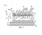
- wirebonds 96, 98 are coupled to metal interconnects 86 of metallization path 80 and wirebond 100 is bonded to metal interconnects 84 by a wirebonding process.
- wirebonds 96, 98, 100 are copper.
- wirebonds 96, 98 are provided having a heavier gauge or greater diameter than wirebond 100, thereby permitting wirebonds 96, 98 to handle a larger amount of electrical current passing through contact pad 46 with a lower electrical resistance.
- wirebonds 96, 98 may be provided as "heavy" copper wirebonds having a diameter of approximately 10-20 mils.
- wirebond 100 may be provided as a "thin" copper wirebond relative to wirebonds 96, 98, having a diameter ranging from approximately 3-10 mils, for example.
- the surface contact area 102 between heavy wirebonds 96, 98 and metallization path 80 may be approximately 50 mils by 80 mils.
- the surface contact area 104 between thin gauge wirebond 100 and metallization path 80 may be in the range of approximately 10-15 mils by 20 mils, for example.
- the width of surface contact areas 102, 104 is two to three times the diameter of the respective wirebond 96, 98, 100, and the length of surface contact areas 102, 104 is four to five times the diameter of the respective wirebond 96, 98, 100.
- embodiments of the invention are not limited to a particular wire gauge used for wirebonds 96, 98, 100 and that the diameter or gauge of wirebonds 96, 98, 100 may be varied as desired for a given application and the corresponding surface contact area will change accordingly.
- a multi-layer substrate 106 is thermally and electrically coupled to contact pad 62 of the semiconductor device 38 via a solder 108.
- multi-layer substrate 106 is a prefabricated direct bond copper (DBC) component that includes a non-organic ceramic substrate 110 such as, for example, alumina, aluminum nitride, silicon nitride, etc., with upper and lower sheets of copper 112, 114 bonded to both sides thereof via a direct bond copper interface or braze layer.
- DBA direct bond aluminum
- semiconductor device 38 is provided having a thickness 116 of approximately 50-500 microns.
- the thickness 118 of metallization path 80 may be in the range of approximately 5-150 microns, while the thickness 120 of dielectric layer 74 may be approximately 0.5-2 mils.
- each wirebond 96, 98, 100 is coupled to a respective portion 122, 124, 126 of POL interconnect layer 88 that includes at least one metal interconnect 84, 86 or a portion thereof.
- the portion 126 of POL interconnect layer 88 beneath the contact surface 128 of wirebond 100 includes one metal interconnect 84
- the portions 122, 124 of POL interconnect layer 88 beneath respective contact surfaces 130, 132 of wirebonds 96, 98 each include portions of at least two metal interconnects 86.
- Metal interconnects 86 thus form multiple parallel paths for current to travel from semiconductor device 38 into wirebonds 96, 98.
- FIGS. 8 and 9 illustrate the positioning of wirebond 96 within a POL structure 134 according to another embodiment of the invention. Elements and components common to POL structure 134 and POL structure 34 are referred to herein with similar part numbers as appropriate.
- wirebond 96 is positioned within a depression or well 136 formed within dielectric layer 74.
- the well 136 is formed by creating a large via 138 within adhesive layer 76 and dielectric layer 74 that exposes a portion of contact pad 46 having a surface area 140 greater than a surface area surface area 142 of the wirebond 96.
- metallization path 80 When metallization path 80 is created, the metallization path 80 extends into via 138 and forms a metal interconnect 144 having a relatively planar upper contact surface 146.
- a surface area 148 of the upper contact surface 146 is greater than a corresponding surface area 142 of wirebond 96.
- the contact surface 150 of wirebond 96 is positioned below the top surface 152 of metallization path 80.
- metallization path 80 is in direct contact with contact pad 46, without any portion of adhesive layer 76 or dielectric layer 74 positioned therebetween, as illustrated in FIG. 9 .
- a portion 154 of POL structure 134 beneath the contact surface 150 of wirebond 96 is substantially free of any portion of the dielectric layer 74 or the adhesive layer 76.
- the increased surface area of metallization path 80 and contact pad 46 decreases the resistance in the current path between contact pad 46 and wirebond 96.
- wirebond 96 is positioned at the same height as the top surface 152 of metallization path 80.
- portion 154 of POL structure 134 beneath contact surface 150 of wirebond 96 is still substantially free of any portion of the dielectric layer 74 or the adhesive layer 76.
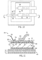
- a POL structure 156 is illustrated according to an alternative embodiment of the invention. Again, common elements to POL structure 156 and POL structure 34 are referred to with similar reference numbers as appropriate.
- wirebonds 96, 100 are coupled to metallization path 80 at in a portion of POL structure 156 that is free of vias 78.
- none of vias 78 are located within the portions 158, 160 of the dielectric layer 74 positioned directly underneath the respective contact locations 162, 164 of the wirebonds 96, 100.
- the thickness 120 of the dielectric layer 74 is substantially uniform in portion of POL structure 156 beneath wirebonds 96, 100 and acts as a stress buffer to reduce potential damage to semiconductor device 38 during the wirebonding process.
- wirebonds 96, 98, 100 and DBC substrate 106 are described above as being coupled to an individual semiconductor device 38 in FIGS. 7-11 , it is contemplated that DBC substrate 106 and/or wirebonds 96, 98, 100 may be applied to respective semiconductor devices 38, 40, 42 at the wafer level (i.e., prior to singulation).
- a POL interconnect layer 166 may be simultaneously formed on multiple individual semiconductor devices provided within a package or reconstituted wafer.
- a reconstituted wafer 168 is shown having a plurality of semiconductor devices 170, 172, coupled to a removable support structure 174.
- semiconductor devices 170, 172 include a plurality of upper contact pads 176, 178, 180, 182, and at least one lower contact pad or collector pad 184, 186.
- Upper contact pads 176-182 may comprise various combinations of emitter and/or gate pads. In a preferred embodiment upper contact pads 176-182 are aluminum or copper. However, it is contemplated that upper contact pads 176-182 may comprise alternative metallization materials.
- semiconductor devices 170, 172 are of varying thicknesses 188, 190, with the thickness 188 of semiconductor device 170 greater than the thickness 190 of semiconductor device 172.
- a shim 192 may be positioned between a thinner semiconductor device and the removable support structure 174 such that an upper surface 194 of the contact pads 176, 178 of semiconductor device 170 are substantially coplanar with an upper surface 196 of the contact pads 180, 182 of semiconductor device 172 within the wafer 168.
- POL interconnect layer 166 is formed atop semiconductor devices 170, 172 in a similar manner as described with respect to FIGS. 3-5 .
- dielectric layer 200 it is contemplated that a single adhesive layer may be spin coated onto dielectric layer 200 in a similar manner as described with respect to dielectric layer 74 ( FIG. 3 ), or individual layers of adhesive 202, 204 may be formed atop each semiconductor device 170, 172 as shown in FIG. 11 . In either case, dielectric layer 200 is positioned to span a gap 206 between the adjacent semiconductor devices 170, 172.
- Dielectric layer 200 may be in the form of a lamination or a film, according to various embodiments, and may be formed of one of a plurality of dielectric materials, similar to dielectric layer 74.
- the semiconductor devices 170, 172 are coupled to dielectric layer 200 via respective adhesive layers 202, 204 (or a single adhesive layer).
- the semiconductor devices 170, 172 are coupled to the dielectric layer 200 by placing them on the adhesive layers 202, 204, as opposed to applying the dielectric layer 200 to the semiconductor devices 170, 172.
- the removable support structure 174 may be omitted.
- a POL interconnect layer 208 may be formed having a dielectric layer 210 constructed to compensate for the differing thicknesses 188, 190 of semiconductor devices 170, 172.
- a first portion 212 of dielectric layer 210 that is aligned with semiconductor device 170 has a first thickness 214 and a second portion 216 of dielectric layer 210 that is aligned with semiconductor device 172 has a second thickness 218.
- a step 220 is positioned at the transition between first portion 212 and second portion 216.
- the differing heights of semiconductor devices 170, 172 may be compensated by varying thicknesses of adhesive layers 202, 204.
- each POL interconnect layer 166 a plurality of vias 222 are formed through dielectric layer 200 and adhesive layers 202, 204, to expose contact pads 176, 178, 180, 182.
- a metallization path 224 is formed on an upper surface 226 of dielectric layer 200.
- Metallization path 224 includes metal interconnects 228 that extend through vias 222 and electrically couple with contact pads 176, 180, and metal interconnects 230 that extend through vias 222 and electrically couple with contact pads 178, 182, 214.
- Metallization paths 224 may comprise a layer of copper, and may be formed using a sputtering and plating technique, followed by a lithography process.
- POL interconnect layer 166 or POL interconnect layer 208 support structure 174 and any shims 192 may be removed if desired.
- Each resulting POL assembly 232, 234 may then be sawn or singulated into individual POL structures having one or multiple semiconductor devices.
- the portion of the dielectric layer 200, 210 residing within gap 206 may be removed, such as by laser ablation, or retained to provide additional structural rigidity to the POL structure.
- Wirebonds may be coupled to metal interconnects 228, 230 in a similar manner as described with respect to any of FIGS. 7-11 either prior to singulation or after.
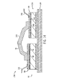
- each POL structure 90, 236 includes a respective POL interconnect layer 88 to which wirebonds 96, 100, 240, 242 of respective POL structures 90, 236 are coupled. Wirebonds 96, 240 electrically couple contact pad 46 of semiconductor device 38 with a contact pad 244 of semiconductor device 246. While FIG. 14 shows POL structures 90, 236 as having different heights, it is contemplated that POL structures 90, 236 may have the same height.
- POL structures 90, 236 are thermally coupled to the same multilayer substrate 106, as shown in FIG. 14 .
- POL structures 90, 236 may be thermally coupled to separate multilayer substrates 106.
- multilayer substrate 106 may be a DBC substrate or a DBA substrate in alternative embodiments.
- FIG. 15 shows an alternative embodiment of a POL assembly 238 in which the singulated POL structures 90, 236 described with respect to FIG. 14 are replaced with reconstituted wafer 232 having at least two semiconductor devices 170, 172.
- POL interconnect layer 166 is formed across the upward-facing surfaces of both semiconductor devices 170, 172 and spans the gap between semiconductor devices 170, 172. While FIG. 15 depicts semiconductor devices 170, 172 as being thermally coupled to the same multilayer substrate 106, it is contemplated that each semiconductor device 170, 172 may be coupled to its own separate multilayer substrate 106.
- Wirebonds 96, 100, 240, 242 are coupled to the POL interconnect layer 166.
- metallization path 224 electrically connects contact pads 176, 178, 180, 182 of semiconductor devices 170, 172 of POL assembly 238.
- semiconductor devices 170, 172 may be electrically coupled to one another without a direct connection between wirebonds 96, 240.
- Wirebonds 96, 240 may thus be used to electrically couple POL assembly 238 to other POL assemblies.
- embodiments of the present invention provide a POL structure that allows copper wirebonding regardless of the material of the contact pads of the semiconductor device.
- the POL interconnect layer provides a copper metallization path that is electrically connected to the contact pads of the semiconductor device and that forms a contact surface to which copper wirebonds may be reliably attached. This permits the use of copper wirebonds in POL modules that include different types of power devices that have different metallization layers, such as copper and aluminum contact pads, for example.
- the resulting POL structure also provides more efficient current distribution from the semiconductor power device to the wirebonds than prior art structures.
- the metalized interconnect structure provided within the POL interconnect layer provides parallel paths for the current to travel from the thin metallization of the contact pads of the power device before entering the wirebonds.
- the thickness of the POL interconnect layer forms a protective buffer layer between the wirebonds and the power device that protects the power device from the higher energies associated with copper-to-copper wirebonding as compared to aluminum-to-aluminum wirebonding. Because the POL interconnect layer acts as a stress buffer for the power device during the wirebonding process, wirebonds having a heavier gauge than those used for traditional copper-to-copper wirebonding may be electrically coupled to the power device without risk of damage to the device. These heavier gauge wirebonds further reduce the interconnect resistance, and hence the associated losses, between the power device and wirebonds.
- a power overlay (POL) structure includes a power device having at least one upper contact pad disposed on an upper surface of the power device, and a POL interconnect layer having a dielectric layer coupled to the upper surface of the power device and a metallization layer having metal interconnects extending through vias formed through the dielectric layer and electrically coupled to the at least one upper contact pad of the power device.
- the POL structure also includes at least one copper wirebond directly coupled to the metallization layer.
- a method of manufacturing a POL structure includes providing a wafer comprising a plurality of semiconductor devices, coupling a dielectric layer to an upper surface of the each of the plurality of semiconductor devices, forming a plurality of vias through the dielectric layer to expose at least one contact pad of the plurality of semiconductor devices, and forming a metallization layer on an upper surface f the dielectric layer, the metallization layer having metal interconnects that extend through the plurality of vias and electrically couple with the at least one contact pad of the plurality of semiconductor devices.
- the method further includes coupling at least one wirebond to a top surface of the metallization layer.
- a POL assembly includes a first semiconductor device, a second semiconductor device, and a POL interconnect assembly having a polymide film adhesively coupled to upper contact pads of the first and second semiconductor devices and a metallization path formed on the polymide film, the metallization path comprising a plurality of metal interconnects extending through vias formed through the polymide film and electrically coupled to the upper contact pads of the first and second semiconductor devices.
- the POL assembly also includes a plurality of copper wirebonds directly coupled to the metallization path, wherein a first wirebond of the plurality of copper wirebonds is electrically coupled to an upper contact pad of the first semiconductor device, and wherein a second wirebond of the plurality of copper wirebonds is electrically coupled to an upper contact pad of the second semiconductor device.
Landscapes
- Wire Bonding (AREA)
- Internal Circuitry In Semiconductor Integrated Circuit Devices (AREA)
- Engineering & Computer Science (AREA)
- Manufacturing & Machinery (AREA)
- Physics & Mathematics (AREA)
- Geometry (AREA)
Abstract
Description
- Embodiments of the invention relate generally to structures and methods for wirebonding of power devices and, more particularly, to a power overlay (POL) structure that enables copper wirebonding of power devices regardless of the material type of the contact pads of the power device.
- Power semiconductor devices are semiconductor devices used as switches or rectifiers in power electronic circuits, such as switched mode power supplies, for example. In use, power semiconductor devices are typically mounted to an external circuit by way of a packaging structure, with the packaging structure providing an electrical connection to the external circuit and also providing a way to remove the heat generated by the devices and protect the devices from the external environment. Power semiconductor devices are provided with a number of input/output (I/O) interconnections to electrically connect the device to an external circuit. These I/O connections may be provided in the form of solder balls, plated bumps, or wirebond connections. In the case of wirebond packaging, wirebonds are provided that connect bond pads or contact pads provided on the power semiconductor device to a corresponding pad or conductive element at the next level of packaging, which may be a circuit board or leadframe. Most existing power device packaging structures use a combination of wirebonds and a substrate (e.g., a direct bonded copper (DBC) substrate) to provide I/O interconnections to both sides of a respective semiconductor device. The packaging structures may be leaded (leadframe, etc.) or provided with bolted terminals for providing electrical connectivity to the packaging structure. The wirebonds form electrical connections from one surface of the packaging structure to package pins, which then interface to the external circuit, and the DBC substrate electrically couples the other surface of the packaging structure to the external circuit.
-
FIG. 1 depicts a wirebondedpower package structure 10, according to known prior art, having asemiconductor device 12 with agate contact pad 14 and anemitter contact pad 16 coupled to anupper surface 18 ofsemiconductor device 12. As shown,wirebonds contact pads semiconductor device 12. In order to form reliable connections between thewirebonds upper contact pads semiconductor device 12, the material of thewirebonds upper contact pads - A
collector pad 26, often in the form of a nickel-gold metallization or a nickel-silver metallization, is formed on alower surface 28 ofsemiconductor device 12. Asolder 30 or sintered silver die attach material is used to couple thesemiconductor device 12 to a DBC or direct bond aluminum (DBA)substrate 32. - Because power devices are typically manufactured with aluminum contact pads, the corresponding wirebonds are likewise formed of aluminum or an aluminum alloy in order to create a reliable electrical connection to the power device. Currently, there is a trend in the industry toward copper wirebonds, which provide lower electrical resistance, which leads to lower losses and higher efficiencies. However, copper wirebonds do not form reliable electrical connections to the aluminum metallization of the contact pads.
- While copper contact pads could be incorporated into the power device at the time of manufacture, incorporating copper into the power device fabrication process is non-trivial and adds significant development cost and time. Also, manufacturers typically provide a single type of metallization material on all of the power devices that they manufacture. Given that a power module may incorporate power devices from multiple manufacturers, forming reliable wirebonds on those power devices is difficult because the various power devices within the given module could include dissimilar metallization materials.
- Even where a power device is provided with copper metallization, coupling copper wirebonds to the copper metallization poses difficulties. For example, attaching a copper wirebond, especially a heavy gauge copper wirebond capable of withstanding high current transients, to a metallization or contact pad applies a greater amount of stress to the power device than a thinner gauge or aluminum wirebond. This is because copper to copper wirebonding requires higher energy for bonding due to its material properties compared to aluminum to aluminum wirebonding. Due to these higher energies, the wirebonding process can damage the power device.
- Another issue with copper-to-copper wirebonding is the constriction of current as it flows from the contact pads of the power device to the wirebonds. The metallization layer of a contact pad on the power device is thin (e.g., a few microns) and the current must travel through this thin metallization until it encounters a wirebond and then flows through it. Wirebonds can be placed only at certain intervals due to equipment constraints, hence each power device will have only a handful wirebonds distributed across the contact pad. While providing a number of wirebonds for each contact pad helps in distributing the current flow, the resistance in the interconnect structure still results in inherent losses.
- While prior attempts have been made to mitigate the above-described problems assocated with copper-to-copper wirebonding, such as by optimizing the copper material properties of the contact pads and adjusting the thickness of the copper pads, there is room for further improvement in the field.
- Therefore, it would be desirable to provide a POL structure that allows for the use of copper wirebonds without changing the metallization of the contact pads of the power device to copper. It would also be desirable to have a method for fabricating an I/O interconnection in the form of a wirebond that reduces device damage due to the applied stresses during the wirebonding process, thereby increasing process yield, and that provides for efficient current distribution from the power device to the wirebonds.
- In accordance with one aspect of the invention, a power overlay (POL) structure includes a power device having at least one upper contact pad disposed on an upper surface of the power device, and a POL interconnect layer having a dielectric layer coupled to the upper surface of the power device and a metallization layer having metal interconnects extending through vias formed through the dielectric layer and electrically coupled to the at least one upper contact pad of the power device. The POL structure also includes at least one copper wirebond directly coupled to the metallization layer.
- In accordance with another aspect of the invention, a method of manufacturing a POL structure includes providing a wafer comprising a plurality of semiconductor devices, coupling a dielectric layer to an upper surface of the each of the plurality of semiconductor devices, forming a plurality of vias through the dielectric layer to expose at least one contact pad of the plurality of semiconductor devices, and forming a metallization layer on an upper surface f the dielectric layer, the metallization layer having metal interconnects that extend through the plurality of vias and electrically couple with the at least one contact pad of the plurality of semiconductor devices. The method further includes coupling at least one wirebond to a top surface of the metallization layer.
- In accordance with yet another aspect of the invention, a POL assembly includes a first semiconductor device, a second semiconductor device, and a POL interconnect assembly having a polymide film adhesively coupled to upper contact pads of the first and second semiconductor devices and a metallization path formed on the polymide film, the metallization path comprising a plurality of metal interconnects extending through vias formed through the polymide film and electrically coupled to the upper contact pads of the first and second semiconductor devices. The POL assembly also includes a plurality of copper wirebonds directly coupled to the metallization path, wherein a first wirebond of the plurality of copper wirebonds is electrically coupled to an upper contact pad of the first semiconductor device, and wherein a second wirebond of the plurality of copper wirebonds is electrically coupled to an upper contact pad of the second semiconductor device.
- These and other advantages and features will be more readily understood from the following detailed description of preferred embodiments of the invention that is provided in connection with the accompanying drawings.
- The drawings illustrate embodiments presently contemplated for carrying out the invention.
- In the drawings:
-
FIG. 1 is a schematic cross-sectional side view of a wirebonded power package structure, according to known prior art. -
FIGS. 2-6 are schematic cross-sectional side views during various stages of manufacturing a power overlay (POL) structure in accordance with an embodiment of the invention. -
FIG. 7 is a schematic cross-sectional side view of one of the POL structures ofFIG. 6 incorporating wirebonds, according to another embodiment of the invention. -
FIGS. 8 and 9 are schematic top and cross-sectional side views of a POL structure with wirebonds, according to an alternative embodiment of the invention. -
FIGS. 10 and 11 are schematic top and cross-sectional side views of a POL structure with wirebonds, according to yet another embodiment of the invention. -
FIG. 12 is a schematic cross-sectional side view showing a reconstituted wafer incorporating POL structures, according to an embodiment of the invention. -
FIG. 13 is a schematic cross-sectional side view showing a reconstituted wafer incorporating POL structures, according to another embodiment of the invention. -
FIG. 14 is a schematic cross-sectional side view of a POL assembly, according to an embodiment of the invention. -
FIG. 15 is a schematic cross-sectional side view of a POL assembly, according to another embodiment of the invention. - Embodiments of the present invention provide for a power overlay (POL) structure including a POL interconnect layer, as well as a method of forming such a POL structure. As used herein, the term "POL" describes a structure that enables copper wirebonding of power devices regardless of the material type of the contact pads of the power device. The POL interconnect layer allows for the reliable connection of copper wirebonds to the POL structure regardless of the material of the gate and emitter pads. In addition, the POL interconnect layer is designed to function as a stress buffer that reduces damage to the power device during the process of attaching the wirebonds to the device contact pads. By providing parallel paths for the current to flow through the metallization of the power device before it enters the wirebonds, the POL structure disclosed herein has reduced interconnect resistance and losses as compared to prior art wirebonded power devices.
-
FIGS. 2-6 depict a technique for manufacturing aPOL structure 34, according to an embodiment of the invention, with each ofFIGS. 2-6 illustrating a cross-section of thePOL structure 34 during the build-up process. Referring first toFIG. 2 , awafer 36 is shown. According to one embodiment,wafer 36 includes a plurality of semiconductor dies orsemiconductor devices Semiconductor devices FIG. 2 shows wafer 36 having threesemiconductor devices wafer 36 may include more or less than three semiconductor devices. - Each
semiconductor device upper contact pads upper surface respective semiconductor device semiconductor device semiconductor device semiconductor device semiconductor device respective semiconductor device semiconductor device 38 includesgate pad 44 andemitter pad 46,semiconductor device 40 includesgate pad 48 andemitter pad 50, andsemiconductor device 42 includesgate pad 52 andemitter pad 54. It is contemplated that semiconductor die 38, 40, 42 may be provided having a differing number of contact pads and/or differing combinations of contact pads than those described above. As one non-limiting example, semiconductor die 38 may be provided having a pair of emitter pads. In oneembodiment contact pads contact pads semiconductor device collector pad lower surface respective semiconductor device - As shown in
FIG. 3 , fabrication ofPOL structure 34 begins with coupling adielectric layer 74 to theupper surfaces semiconductor devices adhesive layer 76.Dielectric layer 74 may be in the form of a stable, non-flowing lamination or a film, according to various embodiments, and may be formed of one of a plurality of dielectric materials, such as Kapton®, Ultem®, polytetrafluoroethylene (PTFE), Upilex®, polysulfone materials (e.g., Udel®, Radel®), or another polymer film, such as a liquid crystal polymer (LCP) or a polyimide material. In one embodiment,dielectric layer 74 may be stretched on a frame (not shown) to control distortion during the fabrication process. Theadhesive layer 76 may be applied todielectric layer 74 using a spin coating technique after whichwafer 36 is placed intoadhesive layer 76 using conventional pick and place equipment and methods. - While
FIG. 3 depictsPOL structure 34 has having separate dielectric andadhesive layers - Referring now to
FIG. 4 , a plurality ofvias 78 are formed throughdielectric layer 74 andadhesive layer 76 to exposecontact pads semiconductor device Vias 78 may be formed by, but not limited to, laser drilling or dry etching, for example. As shown inFIG. 5 , metallization path ormetallization layer 80 is formed on anupper surface 82 ofdielectric layer 74 in a next step of the fabrication process.Metallization layer 80 includes a first portion ofmetal interconnects 84 that extend throughvias 78 and are electrically coupled to contactpads semiconductor devices metal interconnects 86 that extend throughvias 78 and are electrically coupled to contactpads semiconductor devices metallization paths 80 comprise a layer of copper. However, it is contemplated that the manufacturing technique may be extended to the use of other electrically conducting materials formetallization paths 80. In one embodiment,metallization paths 80 may be formed using a sputtering and plating technique, followed by a lithography process. Together,metallization paths 80, vias 78,dielectric layer 74, andadhesive layer 76 form aPOL interconnect layer 88. - Referring now to
FIG. 6 ,POL structure 34 is sawn or singulated intoindividual POL structures POL structure respective semiconductor device POL interconnect layer 88 bonded thereto. Aswafer 36 may include more or less than threesemiconductor devices POL structure 34 may be separated into more or less than threePOL structures - Now referring to
FIG. 7 , afterPOL structure 34 has been sawn or singulated intoindividual POL structures metallization path 80 in a next step of the manufacturing technique. In the illustrated embodiment, wirebonds 96, 98 are coupled tometal interconnects 86 ofmetallization path 80 andwirebond 100 is bonded tometal interconnects 84 by a wirebonding process. However, it is contemplated that alternative embodiments may incorporate more or less than two wirebonds bonded to the second portion ofmetal interconnects 86 and/or more than onewirebond 100 bonded to the first portion of metal interconnects 84. According to an exemplary embodiment of the invention, wirebonds 96, 98, 100 are copper. - In one embodiment, wirebonds 96, 98 are provided having a heavier gauge or greater diameter than
wirebond 100, thereby permittingwirebonds contact pad 46 with a lower electrical resistance. As one non-limiting example, wirebonds 96, 98 may be provided as "heavy" copper wirebonds having a diameter of approximately 10-20 mils. Meanwhile, wirebond 100 may be provided as a "thin" copper wirebond relative to wirebonds 96, 98, having a diameter ranging from approximately 3-10 mils, for example. In such a non-limiting embodiment of the invention, thesurface contact area 102 betweenheavy wirebonds metallization path 80 may be approximately 50 mils by 80 mils. On the other hand, thesurface contact area 104 betweenthin gauge wirebond 100 andmetallization path 80 may be in the range of approximately 10-15 mils by 20 mils, for example. In an exemplary embodiment of the invention, the width ofsurface contact areas respective wirebond surface contact areas respective wirebond wirebonds - A
multi-layer substrate 106 is thermally and electrically coupled to contactpad 62 of thesemiconductor device 38 via asolder 108. In one embodiment,multi-layer substrate 106 is a prefabricated direct bond copper (DBC) component that includes a non-organicceramic substrate 110 such as, for example, alumina, aluminum nitride, silicon nitride, etc., with upper and lower sheets ofcopper multi-layer substrate 106 may be a direct bond aluminum (DBA) substrate having upper andlower aluminum sheets - While
FIG. 7 and subsequent figures depict amulti-layer substrate 106 thermally and electrically coupled to contactpad 62, it is contemplated that alternative embodiments may include a single layer substrate such as, for example, a leadframe instead ofmulti-layer substrate 106. - As shown in
FIG. 7 ,semiconductor device 38 is provided having athickness 116 of approximately 50-500 microns. In addition, thethickness 118 ofmetallization path 80 may be in the range of approximately 5-150 microns, while thethickness 120 ofdielectric layer 74 may be approximately 0.5-2 mils. - In the embodiment illustrated in
FIG. 7 , each wirebond 96, 98, 100 is coupled to arespective portion POL interconnect layer 88 that includes at least onemetal interconnect portion 126 ofPOL interconnect layer 88 beneath thecontact surface 128 ofwirebond 100 includes onemetal interconnect 84, and theportions POL interconnect layer 88 beneath respective contact surfaces 130, 132 ofwirebonds metal interconnects 86. Metal interconnects 86 thus form multiple parallel paths for current to travel fromsemiconductor device 38 intowirebonds -
FIGS. 8 and 9 illustrate the positioning ofwirebond 96 within aPOL structure 134 according to another embodiment of the invention. Elements and components common toPOL structure 134 andPOL structure 34 are referred to herein with similar part numbers as appropriate. As shown,wirebond 96 is positioned within a depression or well 136 formed withindielectric layer 74. The well 136 is formed by creating a large via 138 withinadhesive layer 76 anddielectric layer 74 that exposes a portion ofcontact pad 46 having asurface area 140 greater than a surfacearea surface area 142 of thewirebond 96. Whenmetallization path 80 is created, themetallization path 80 extends into via 138 and forms a metal interconnect 144 having a relatively planarupper contact surface 146. Asurface area 148 of theupper contact surface 146 is greater than acorresponding surface area 142 ofwirebond 96. Thus, thecontact surface 150 ofwirebond 96 is positioned below thetop surface 152 ofmetallization path 80. In this embodiment,metallization path 80 is in direct contact withcontact pad 46, without any portion ofadhesive layer 76 ordielectric layer 74 positioned therebetween, as illustrated inFIG. 9 . Thus, aportion 154 ofPOL structure 134 beneath thecontact surface 150 ofwirebond 96 is substantially free of any portion of thedielectric layer 74 or theadhesive layer 76. In this embodiment, the increased surface area ofmetallization path 80 andcontact pad 46 decreases the resistance in the current path betweencontact pad 46 andwirebond 96. - In another embodiment, it is contemplated that, when
metallization path 80 is created by extending into via 138 and forming metal interconnects 144, the planarupper contact surface 146 and thesurface 152 ofmetallization path 80 are coplanar. As such,wirebond 96 is positioned at the same height as thetop surface 152 ofmetallization path 80. In this embodiment,portion 154 ofPOL structure 134 beneathcontact surface 150 ofwirebond 96 is still substantially free of any portion of thedielectric layer 74 or theadhesive layer 76. - Referring now to
FIGS. 10 and 11 , aPOL structure 156 is illustrated according to an alternative embodiment of the invention. Again, common elements toPOL structure 156 andPOL structure 34 are referred to with similar reference numbers as appropriate. As shown, wirebonds 96, 100 are coupled tometallization path 80 at in a portion ofPOL structure 156 that is free ofvias 78. Thus, in this embodiment, none ofvias 78 are located within theportions dielectric layer 74 positioned directly underneath therespective contact locations wirebonds thickness 120 of thedielectric layer 74 is substantially uniform in portion ofPOL structure 156 beneathwirebonds semiconductor device 38 during the wirebonding process. - While wirebonds 96, 98, 100 and
DBC substrate 106 are described above as being coupled to anindividual semiconductor device 38 inFIGS. 7-11 , it is contemplated thatDBC substrate 106 and/orwirebonds respective semiconductor devices - In an alternative embodiment, a
POL interconnect layer 166 may be simultaneously formed on multiple individual semiconductor devices provided within a package or reconstituted wafer. Referring now toFIG. 12 , areconstituted wafer 168 is shown having a plurality ofsemiconductor devices removable support structure 174. One having ordinary skill in the art would recognize thatreconstituted wafer 168 may include more than twosemiconductor devices semiconductor devices FIGS. 2-6 ,semiconductor devices upper contact pads collector pad - As shown in
FIG. 12 semiconductor devices thicknesses thickness 188 ofsemiconductor device 170 greater than thethickness 190 ofsemiconductor device 172. To account for this variance in thickness, ashim 192 may be positioned between a thinner semiconductor device and theremovable support structure 174 such that anupper surface 194 of thecontact pads semiconductor device 170 are substantially coplanar with anupper surface 196 of thecontact pads semiconductor device 172 within thewafer 168. - Once upper surfaces 194-196 of
semiconductor devices POL interconnect layer 166 is formed atopsemiconductor devices FIGS. 3-5 . In applyingdielectric layer 200 tosemiconductor devices dielectric layer 200 in a similar manner as described with respect to dielectric layer 74 (FIG. 3 ), or individual layers of adhesive 202, 204 may be formed atop eachsemiconductor device FIG. 11 . In either case,dielectric layer 200 is positioned to span agap 206 between theadjacent semiconductor devices Dielectric layer 200 may be in the form of a lamination or a film, according to various embodiments, and may be formed of one of a plurality of dielectric materials, similar todielectric layer 74. - In an alternative embodiment of the invention, the
semiconductor devices dielectric layer 200 via respectiveadhesive layers 202, 204 (or a single adhesive layer). Here, thesemiconductor devices dielectric layer 200 by placing them on theadhesive layers dielectric layer 200 to thesemiconductor devices removable support structure 174 may be omitted. - In another embodiment of the invention, illustrated in
FIG. 13 , aPOL interconnect layer 208 may be formed having adielectric layer 210 constructed to compensate for thediffering thicknesses semiconductor devices first portion 212 ofdielectric layer 210 that is aligned withsemiconductor device 170 has afirst thickness 214 and asecond portion 216 ofdielectric layer 210 that is aligned withsemiconductor device 172 has asecond thickness 218. Astep 220 is positioned at the transition betweenfirst portion 212 andsecond portion 216. In yet another embodiment of the invention, the differing heights ofsemiconductor devices adhesive layers - Referring to
FIGS. 12 and 13 together, to complete eachPOL interconnect layer 166, a plurality ofvias 222 are formed throughdielectric layer 200 andadhesive layers contact pads metallization path 224 is formed on anupper surface 226 ofdielectric layer 200.Metallization path 224 includesmetal interconnects 228 that extend throughvias 222 and electrically couple withcontact pads metal interconnects 230 that extend throughvias 222 and electrically couple withcontact pads Metallization paths 224 may comprise a layer of copper, and may be formed using a sputtering and plating technique, followed by a lithography process. - Following formation of
POL interconnect layer 166 orPOL interconnect layer 208,support structure 174 and anyshims 192 may be removed if desired. Each resultingPOL assembly dielectric layer gap 206 may be removed, such as by laser ablation, or retained to provide additional structural rigidity to the POL structure. Wirebonds may be coupled tometal interconnects FIGS. 7-11 either prior to singulation or after. - Now referring to
FIG. 14 , asingulated POL structure 90 is shown electrically coupled with anotherPOL structure 236 within aPOL assembly 238, in accordance with another embodiment of the invention. As shown, eachPOL structure POL interconnect layer 88 to which wirebonds 96, 100, 240, 242 ofrespective POL structures Wirebonds couple contact pad 46 ofsemiconductor device 38 with acontact pad 244 ofsemiconductor device 246. WhileFIG. 14 showsPOL structures POL structures - In one
embodiment POL structures same multilayer substrate 106, as shown inFIG. 14 . However, one having ordinary skill in the art would recognize thatPOL structures separate multilayer substrates 106. In addition, it is contemplated thatmultilayer substrate 106 may be a DBC substrate or a DBA substrate in alternative embodiments. - Next,
FIG. 15 shows an alternative embodiment of aPOL assembly 238 in which thesingulated POL structures FIG. 14 are replaced with reconstitutedwafer 232 having at least twosemiconductor devices POL interconnect layer 166 is formed across the upward-facing surfaces of bothsemiconductor devices semiconductor devices FIG. 15 depictssemiconductor devices same multilayer substrate 106, it is contemplated that eachsemiconductor device separate multilayer substrate 106. -
Wirebonds POL interconnect layer 166. In this embodiment,metallization path 224 electrically connectscontact pads semiconductor devices POL assembly 238. As a result,semiconductor devices wirebonds Wirebonds POL assembly 238 to other POL assemblies. - Beneficially, embodiments of the present invention provide a POL structure that allows copper wirebonding regardless of the material of the contact pads of the semiconductor device. The POL interconnect layer provides a copper metallization path that is electrically connected to the contact pads of the semiconductor device and that forms a contact surface to which copper wirebonds may be reliably attached. This permits the use of copper wirebonds in POL modules that include different types of power devices that have different metallization layers, such as copper and aluminum contact pads, for example.
- The resulting POL structure also provides more efficient current distribution from the semiconductor power device to the wirebonds than prior art structures. The metalized interconnect structure provided within the POL interconnect layer provides parallel paths for the current to travel from the thin metallization of the contact pads of the power device before entering the wirebonds.
- Also, the thickness of the POL interconnect layer forms a protective buffer layer between the wirebonds and the power device that protects the power device from the higher energies associated with copper-to-copper wirebonding as compared to aluminum-to-aluminum wirebonding. Because the POL interconnect layer acts as a stress buffer for the power device during the wirebonding process, wirebonds having a heavier gauge than those used for traditional copper-to-copper wirebonding may be electrically coupled to the power device without risk of damage to the device. These heavier gauge wirebonds further reduce the interconnect resistance, and hence the associated losses, between the power device and wirebonds.
- Therefore, according to one embodiment of the invention, a power overlay (POL) structure includes a power device having at least one upper contact pad disposed on an upper surface of the power device, and a POL interconnect layer having a dielectric layer coupled to the upper surface of the power device and a metallization layer having metal interconnects extending through vias formed through the dielectric layer and electrically coupled to the at least one upper contact pad of the power device. The POL structure also includes at least one copper wirebond directly coupled to the metallization layer.
- According to another aspect of the invention, a method of manufacturing a POL structure includes providing a wafer comprising a plurality of semiconductor devices, coupling a dielectric layer to an upper surface of the each of the plurality of semiconductor devices, forming a plurality of vias through the dielectric layer to expose at least one contact pad of the plurality of semiconductor devices, and forming a metallization layer on an upper surface f the dielectric layer, the metallization layer having metal interconnects that extend through the plurality of vias and electrically couple with the at least one contact pad of the plurality of semiconductor devices. The method further includes coupling at least one wirebond to a top surface of the metallization layer.
- According to yet another aspect of the invention, a POL assembly includes a first semiconductor device, a second semiconductor device, and a POL interconnect assembly having a polymide film adhesively coupled to upper contact pads of the first and second semiconductor devices and a metallization path formed on the polymide film, the metallization path comprising a plurality of metal interconnects extending through vias formed through the polymide film and electrically coupled to the upper contact pads of the first and second semiconductor devices. The POL assembly also includes a plurality of copper wirebonds directly coupled to the metallization path, wherein a first wirebond of the plurality of copper wirebonds is electrically coupled to an upper contact pad of the first semiconductor device, and wherein a second wirebond of the plurality of copper wirebonds is electrically coupled to an upper contact pad of the second semiconductor device.
- While the invention has been described in detail in connection with only a limited number of embodiments, it should be readily understood that the invention is not limited to such disclosed embodiments. Rather, the invention can be modified to incorporate any number of variations, alterations, substitutions or equivalent arrangements not heretofore described, but which are commensurate with the spirit and scope of the invention. Additionally, while various embodiments of the invention have been described, it is to be understood that aspects of the invention may include only some of the described embodiments. Accordingly, the invention is not to be seen as limited by the foregoing description, but is only limited by the scope of the appended claims.
- Various aspects and embodiments of the present invention are defined by the following numbered clauses:
- 1. A power overlay (POL) structure comprising:
- a power device having at least one upper contact pad disposed on an upper surface of the power device;
a POL interconnect layer comprising:- a dielectric layer coupled to the upper surface of the power device; and
- a metallization layer having metal interconnects extending through vias formed through the dielectric layer and electrically coupled to the at least one upper contact pad of the power device; and
- at least one copper wirebond directly coupled to the metallization layer.
- a power device having at least one upper contact pad disposed on an upper surface of the power device;
- 2. The POL structure of clause 1, wherein the at least upper one contact pad comprises aluminum.
- 3. The POL structure of clause 1 or 2, further comprising a multilayer substrate thermally and electrically coupled to a lower contact pad of the power device with a solder layer, the multilayer substrate comprising one of a direct bond copper (DBC) and a direct bond aluminum (DBA) substrate.
- 4. The POL structure of any preceding clause, wherein the dielectric layer has a substantially uniform thickness beneath a contact location of the at least one copper wirebond.
- 5. The POL structure of any preceding clause, wherein the dielectric layer is coupled to the upper surface of the power device via an adhesive layer.
- 6. The POL structure of any preceding clause, wherein a portion of the POL interconnect layer disposed between a contact surface of the wirebond and the power device is absent the dielectric layer.
- 7. The POL structure of any preceding clause, further comprising:
- a metal interconnect having an upper contact surface positioned below a top surface of the metallization layer; and
- a copper wirebond coupled to the upper contact surface of the metal interconnect;
- wherein a surface area of a contact surface of the upper wirebond is smaller than a surface area of the upper contact surface of the metal interconnect.
- 8. The POL structure of any preceding clause, wherein a contact surface of the at least one wirebond is coupled to a portion of the POL interconnect layer having a metalized interconnect.
- 9. A method of manufacturing a power overlay (POL) structure comprising:
- providing a wafer comprising a plurality of semiconductor devices;
- coupling a dielectric layer to an upper surface of the each of the plurality of semiconductor devices;
- forming a plurality of vias through the dielectric layer to expose at least one contact pad of the plurality of semiconductor devices;
- forming a metallization layer on an upper surface of the dielectric layer, the metallization layer having metal interconnects that extend through the plurality of vias and electrically couple with the at least one contact pad of the plurality of semiconductor devices; and
- coupling at least one wirebond to a top surface of the metallization layer.
- 10. The method of any preceding clause, wherein coupling the dielectric layer to the upper surface of the each of the plurality of semiconductor devices includes disposing an adhesive layer therebetween.
- 11. The method of any preceding clause, further comprising singulating the wafer into a plurality of POL structures, each of the plurality of POL structures comprising at least one semiconductor device having a portion of the dielectric layer and a portion of the metallization layer formed thereon.
- 12. The method of any preceding clause, further comprising:
- forming a via to expose a surface area of a contact pad greater than a surface area of the at least one wirebond; and
- coupling the at least one wirebond to a metal interconnect formed within the via.
- 13. The method of any preceding clause, further comprising coupling the at least one wirebond to a portion of the metallization layer free of metal interconnects.
- 14. The method of any preceding clause, further comprising coupling a removable support structure to a lower surface of the plurality of semiconductor devices prior to coupling the dielectric layer to the upper surface of the plurality of semiconductor devices.
- 15. The method of any preceding clause, further comprising coupling the dielectric layer to a first semiconductor device and a second semiconductor device of the wafer, the first semiconductor device having a thickness greater than a thickness of the second semiconductor device.
- 16. The method of any preceding clause, further comprising positioning the first semiconductor device a distance from the second semiconductor device such that a gap is formed therebetween.
- 17. The method of any preceding clause, further comprising disposing a shim between the support structure and the lower surface of the second semiconductor device such that an upper surface of the first semiconductor device is substantially coplanar with an upper surface of the second semiconductor device.
- 18. The method of any preceding clause, further comprising:
- coupling a first portion of the dielectric layer to the first semiconductor device; and
- coupling a second portion of the dielectric layer to the second semiconductor device, wherein a thickness of the second portion of the dielectric layer is greater than a thickness of the first portion of the dielectric layer.
- 19. A power overlay (POL) assembly comprising:
- a first semiconductor device and a second semiconductor device;
- a POL interconnect assembly comprising:
- a polyimide film adhesively coupled to upper contact pads of the first and second semiconductor devices; and
- a metallization path formed on the polyimide film, the metallization path comprising a plurality of metal interconnects extending through vias formed through the polyimide film and electrically coupled to the upper contact pads of the first and second semiconductor devices; and
- a plurality of copper wirebonds directly coupled to the metallization path;
- wherein a first wirebond of the plurality of copper wirebonds is electrically coupled to an upper contact pad of the first semiconductor device; and
- wherein a second wirebond of the plurality of copper wirebonds is electrically coupled to an upper contact pad of the second semiconductor device.
- 20. The POL assembly of any preceding clause, the at least one copper wirebond of the first POL structure is electrically coupled to the at least one copper wirebond of the second POL structure.
- 21. The POL assembly of any preceding clause, wherein a thickness of the first semiconductor device differs from a thickness of the second semiconductor device; and
wherein the POL assembly comprises at least one of a polyimide film having a variable thickness and a shim coupled to a bottom surface one of the first and second semiconductor devices. - 22. The POL assembly of any preceding clause, wherein the first wirebond is coupled to a portion of the POL interconnect assembly substantially free of the polyimide film.
- 23. The POL assembly of any preceding clause, wherein the first wirebond is coupled to a portion of the POL interconnect assembly wherein the polyimide film has a substantially uniform thickness.
Claims (15)
- A power overlay (POL) structure (34) comprising:a power device (38,40,42) having at least one upper contact pad (44,46,48,50,52,54) disposed on an upper surface (56,58,60) of the power device (38,40,42);a POL interconnect layer (88) comprising:a dielectric layer (74) coupled to the upper surface (56,58,60) of the power device (38,40,42); anda metallization layer (80) having metal interconnects (86) extending through vias (78) formed through the dielectric layer (74) and electrically coupled to the at least one upper contact pad (44-54) of the power device (38,40,42); andat least one copper wirebond (96,98,100) directly coupled to the metallization layer.
- The POL structure of claim 1 or 2, further comprising a multilayer substrate (106) thermally and electrically coupled to a lower contact pad (62) of the power device (38,40,42) with a solder layer (108), the multilayer substrate (106) comprising one of a direct bond copper (DBC) and a direct bond aluminum (DBA) substrate (110).
- The POL structure of any claims 1 to 3, wherein the dielectric layer (74) has a substantially uniform thickness beneath a contact location of the at least one copper wirebond (96,98,100).
- The POL structure of any preceding claim, wherein the dielectric layer (76) is coupled to the upper surface (56,58,60) of the power device (38,40,42) via an adhesive layer (70).
- The POL structure of any preceding claim, further comprising:a metal interconnect (144) having an upper contact surface (146) positioned below a top surface (152) of the metallization layer (80); anda copper wirebond (96) coupled to the upper contact surface (146) of the metal interconnect (144);wherein a surface area (142) of a contact surface of the upper wirebond (96) is smaller than a surface area (148) of the upper contact surface (146) of the metal interconnect (144).
- A method of manufacturing a power overlay (POL) structure (34) comprising:providing a wafer (36) comprising a plurality of semiconductor devices (38,40,42);coupling a dielectric layer (74) to an upper surface (56,58,60) of the each of the plurality of semiconductor devices (38,40,42);forming a plurality of vias (78) through the dielectric layer (74) to expose at least one contact pad (44,46,48, 50, 52,54) of the plurality of semiconductor devices (38,40,42);forming a metallization layer (80) on an upper surface of the dielectric layer (74), the metallization layer (80) having metal interconnects that extend through the plurality of vias (78) and electrically couple with the at least one contact pad (44-54) of the plurality of semiconductor devices (38,40,42); andcoupling at least one wirebond (96,98,100) to a top surface of the metallization layer (80).
- The method of claim 6, wherein coupling the dielectric layer (74) to the upper surface (56,58,60) of the each of the plurality of semiconductor devices (38,40,42) includes disposing an adhesive layer (76) therebetween.
- The method of claim 6 or 7, further comprising singulating the wafer (34) into a plurality of POL structures (90,92,94), each of the plurality of POL structures (90,92,94) comprising at least one semiconductor (38,40,42) device having a portion of the dielectric layer (74) and a portion of the metallization layer (80) formed thereon.
- The method of any of claims 6 to 8, further comprising:forming a via (138) to expose a surface area (140) of a contact pad (46) greater than a surface area (142) of the at least one wirebond (96); andcoupling the at least one wirebond (96) to a metal interconnect (144) formed within the via (138).
- The method of any of claims 6 to 8, further comprising coupling the at least one wirebond (96) to a portion of the metallization layer (80) free of metal interconnects.
- The method of any of claims 6 to 10, further comprising coupling a removable support structure (174) to a lower surface of the plurality of semiconductor devices (170,172) prior to coupling the dielectric layer (200) to the upper surface (194,196) of the plurality of semiconductor devices (170,172).
- The method of any of claims 6 to 11, further comprising coupling the dielectric layer (200) to a first semiconductor device (170) and a second semiconductor device (172) of the wafer (168), the first semiconductor device (170) having a thickness (188) greater than a thickness (190) of the second semiconductor device (172).
- The method of claim 12, further comprising positioning the first semiconductor device (170) a distance from the second semiconductor device (172) such that a gap (206) is formed therebetween.
- The method of claim 11 or 13, further comprising disposing a shim (192) between the support structure (174) and the lower surface of the second semiconductor device (172) such that an upper surface (194) of the first semiconductor device (170) is substantially coplanar with an upper surface (196) of the second semiconductor device (172).
- The method of any of claims 12 to 14, further comprising:coupling a first portion (212) of the dielectric layer (200) to the first semiconductor device (170); andcoupling a second portion (216) of the dielectric layer (210) to the second semiconductor device (172), wherein a thickness (218) of the second portion (216) of the dielectric layer (210) is greater than a thickness (214) of the first portion (212) of the dielectric layer (210).
Applications Claiming Priority (1)
| Application Number | Priority Date | Filing Date | Title |
|---|---|---|---|
| US14/512,562 US9613843B2 (en) | 2014-10-13 | 2014-10-13 | Power overlay structure having wirebonds and method of manufacturing same |
Publications (2)
| Publication Number | Publication Date |
|---|---|
| EP3010038A2 true EP3010038A2 (en) | 2016-04-20 |
| EP3010038A3 EP3010038A3 (en) | 2016-07-20 |
Family
ID=54293117
Family Applications (1)
| Application Number | Title | Priority Date | Filing Date |
|---|---|---|---|
| EP15189400.3A Pending EP3010038A3 (en) | 2014-10-13 | 2015-10-12 | Power overlay structure having wirebonds and method of manufacturing same |
Country Status (6)
| Country | Link |
|---|---|
| US (2) | US9613843B2 (en) |
| EP (1) | EP3010038A3 (en) |
| JP (3) | JP2016082230A (en) |
| KR (1) | KR102419302B1 (en) |
| CN (3) | CN116544208A (en) |
| TW (1) | TWI713470B (en) |
Cited By (1)
| Publication number | Priority date | Publication date | Assignee | Title |
|---|---|---|---|---|
| WO2022122527A1 (en) * | 2020-12-08 | 2022-06-16 | Hitachi Energy Switzerland Ag | Semiconductor module and manufacturing method |
Families Citing this family (21)
| Publication number | Priority date | Publication date | Assignee | Title |
|---|---|---|---|---|
| US9613843B2 (en) * | 2014-10-13 | 2017-04-04 | General Electric Company | Power overlay structure having wirebonds and method of manufacturing same |
| DE102015102535B4 (en) * | 2015-02-23 | 2023-08-03 | Infineon Technologies Ag | Bonding system and method for bonding a hygroscopic material |
| US10056319B2 (en) * | 2016-04-29 | 2018-08-21 | Delta Electronics, Inc. | Power module package having patterned insulation metal substrate |
| JP6726112B2 (en) * | 2017-01-19 | 2020-07-22 | 株式会社 日立パワーデバイス | Semiconductor device and power converter |
| JP7163054B2 (en) * | 2017-04-20 | 2022-10-31 | ローム株式会社 | semiconductor equipment |
| US10541209B2 (en) | 2017-08-03 | 2020-01-21 | General Electric Company | Electronics package including integrated electromagnetic interference shield and method of manufacturing thereof |
| US10541153B2 (en) | 2017-08-03 | 2020-01-21 | General Electric Company | Electronics package with integrated interconnect structure and method of manufacturing thereof |
| US10804115B2 (en) | 2017-08-03 | 2020-10-13 | General Electric Company | Electronics package with integrated interconnect structure and method of manufacturing thereof |
| US10332832B2 (en) | 2017-08-07 | 2019-06-25 | General Electric Company | Method of manufacturing an electronics package using device-last or device-almost last placement |
| USD881189S1 (en) | 2018-02-26 | 2020-04-14 | Samsung Electronics Co., Ltd. | Head-mounted display device |
| US10957832B2 (en) | 2018-10-22 | 2021-03-23 | General Electric Company | Electronics package for light emitting semiconductor devices and method of manufacturing thereof |
| US11538769B2 (en) * | 2018-12-14 | 2022-12-27 | General Electric Company | High voltage semiconductor devices having improved electric field suppression |
| US10892237B2 (en) * | 2018-12-14 | 2021-01-12 | General Electric Company | Methods of fabricating high voltage semiconductor devices having improved electric field suppression |
| JP7472435B2 (en) | 2019-05-13 | 2024-04-23 | 富士電機株式会社 | Semiconductor module manufacturing method |
| CN111162015A (en) * | 2019-12-20 | 2020-05-15 | 珠海格力电器股份有限公司 | A kind of intelligent power module and packaging method |
| US11776870B2 (en) * | 2020-01-16 | 2023-10-03 | Semiconductor Components Industries, Llc | Direct bonded copper substrates fabricated using silver sintering |
| US11398445B2 (en) | 2020-05-29 | 2022-07-26 | General Electric Company | Mechanical punched via formation in electronics package and electronics package formed thereby |
| WO2022029828A1 (en) * | 2020-08-03 | 2022-02-10 | 三菱電機株式会社 | Semiconductor device, semiconductor device manufacturing method, and power conversion device |
| CN112910285B (en) * | 2021-01-05 | 2022-06-14 | 深圳市富鑫产业科技有限公司 | Inverter power system and manufacturing method thereof |
| US11848244B2 (en) * | 2021-09-30 | 2023-12-19 | Texas Instruments Incorporated | Leaded wafer chip scale packages |
| WO2026009326A1 (en) * | 2024-07-02 | 2026-01-08 | 三菱電機株式会社 | Semiconductor device and power conversion device |
Citations (2)
| Publication number | Priority date | Publication date | Assignee | Title |
|---|---|---|---|---|
| DE19612838A1 (en) * | 1995-11-13 | 1997-05-15 | Asea Brown Boveri | Power semiconductor component, e.g. thyristor, for high voltage direct current use |
| DE102007046021B4 (en) * | 2006-10-20 | 2012-09-13 | Infineon Technologies Ag | A semiconductor device, semiconductor module and method for connecting a semiconductor chip to a ceramic substrate |
Family Cites Families (63)
| Publication number | Priority date | Publication date | Assignee | Title |
|---|---|---|---|---|
| FR2599893B1 (en) * | 1986-05-23 | 1996-08-02 | Ricoh Kk | METHOD FOR MOUNTING AN ELECTRONIC MODULE ON A SUBSTRATE AND INTEGRATED CIRCUIT CARD |
| EP0646959B1 (en) * | 1993-09-30 | 2001-08-16 | Consorzio per la Ricerca sulla Microelettronica nel Mezzogiorno | Metallization and bonding process for manufacturing power semiconductor devices |
| US5637922A (en) * | 1994-02-07 | 1997-06-10 | General Electric Company | Wireless radio frequency power semiconductor devices using high density interconnect |
| JP3432284B2 (en) * | 1994-07-04 | 2003-08-04 | 三菱電機株式会社 | Semiconductor device |
| JPH08213420A (en) * | 1995-02-03 | 1996-08-20 | Hitachi Ltd | Semiconductor device |
| JPH0933940A (en) * | 1995-07-14 | 1997-02-07 | Citizen Watch Co Ltd | Mounting structure of semiconductor chip for driving display panel |
| JP3415981B2 (en) * | 1996-01-10 | 2003-06-09 | 株式会社日立製作所 | Semiconductor device, manufacturing method thereof, and surface protective film |
| US6057612A (en) * | 1998-07-02 | 2000-05-02 | Intersil Corporation | Flat power pack |
| US6440641B1 (en) * | 1998-07-31 | 2002-08-27 | Kulicke & Soffa Holdings, Inc. | Deposited thin film build-up layer dimensions as a method of relieving stress in high density interconnect printed wiring board substrates |
| US6232151B1 (en) * | 1999-11-01 | 2001-05-15 | General Electric Company | Power electronic module packaging |
| EP1139413B1 (en) | 2000-03-24 | 2005-03-16 | Texas Instruments Incorporated | Wire bonding process |
| FR2822591A1 (en) * | 2001-03-22 | 2002-09-27 | Commissariat Energie Atomique | ASSEMBLY OF COMPONENTS OF VARIOUS THICKNESSES |
| JP3719994B2 (en) * | 2001-12-28 | 2005-11-24 | 株式会社東芝 | Semiconductor device |
| JP2003347741A (en) * | 2002-05-30 | 2003-12-05 | Taiyo Yuden Co Ltd | Composite multilayer substrate and module using the same |
| US6979891B2 (en) * | 2003-09-08 | 2005-12-27 | Intel Corporation | Integrated circuit packaging architecture |
| US6995475B2 (en) * | 2003-09-18 | 2006-02-07 | International Business Machines Corporation | I/C chip suitable for wire bonding |
| FI117814B (en) * | 2004-06-15 | 2007-02-28 | Imbera Electronics Oy | Procedure for manufacturing an electronics module |
| DE102004043020B3 (en) | 2004-09-06 | 2006-04-27 | eupec Europäische Gesellschaft für Leistungshalbleiter mbH | Bonding wire and bond connection |
| JP4674522B2 (en) * | 2004-11-11 | 2011-04-20 | 株式会社デンソー | Semiconductor device |
| US7327024B2 (en) * | 2004-11-24 | 2008-02-05 | General Electric Company | Power module, and phase leg assembly |
| JP4710700B2 (en) * | 2005-05-09 | 2011-06-29 | 株式会社デンソー | Semiconductor device and manufacturing method thereof |
| JP2007073611A (en) * | 2005-09-05 | 2007-03-22 | Renesas Technology Corp | Electronic device and manufacturing method thereof |
| JP2007109932A (en) * | 2005-10-14 | 2007-04-26 | Toshiba Corp | Semiconductor device |
| US20080190748A1 (en) * | 2007-02-13 | 2008-08-14 | Stephen Daley Arthur | Power overlay structure for mems devices and method for making power overlay structure for mems devices |
| US7884452B2 (en) * | 2007-11-23 | 2011-02-08 | Alpha And Omega Semiconductor Incorporated | Semiconductor power device package having a lead frame-based integrated inductor |
| US8039302B2 (en) * | 2007-12-07 | 2011-10-18 | Stats Chippac, Ltd. | Semiconductor package and method of forming similar structure for top and bottom bonding pads |
| US7947592B2 (en) * | 2007-12-14 | 2011-05-24 | Semiconductor Components Industries, Llc | Thick metal interconnect with metal pad caps at selective sites and process for making the same |
| US7960845B2 (en) | 2008-01-03 | 2011-06-14 | Linear Technology Corporation | Flexible contactless wire bonding structure and methodology for semiconductor device |
| US7839642B2 (en) * | 2008-04-04 | 2010-11-23 | Liebert Corporation | Heat-sink brace for fault-force support |
| JP5331610B2 (en) * | 2008-12-03 | 2013-10-30 | ルネサスエレクトロニクス株式会社 | Semiconductor integrated circuit device |
| US9064936B2 (en) * | 2008-12-12 | 2015-06-23 | Stats Chippac, Ltd. | Semiconductor device and method of forming a vertical interconnect structure for 3-D FO-WLCSP |
| US8592992B2 (en) * | 2011-12-14 | 2013-11-26 | Stats Chippac, Ltd. | Semiconductor device and method of forming vertical interconnect structure with conductive micro via array for 3-D Fo-WLCSP |
| US7915741B2 (en) * | 2009-02-24 | 2011-03-29 | Unisem Advanced Technologies Sdn. Bhd. | Solder bump UBM structure |
| US8358000B2 (en) * | 2009-03-13 | 2013-01-22 | General Electric Company | Double side cooled power module with power overlay |
| TW201113993A (en) * | 2009-10-01 | 2011-04-16 | Anpec Electronics Corp | Pre-packaged structure |
| EP2328172B1 (en) | 2009-10-02 | 2019-06-26 | Abb Research Ltd. | A power-electronic arrangement |
| US8242013B2 (en) * | 2010-03-30 | 2012-08-14 | Alpha & Omega Semiconductor Inc. | Virtually substrate-less composite power semiconductor device and method |
| JP2011222555A (en) * | 2010-04-02 | 2011-11-04 | Denso Corp | Method for manufacturing wiring board with built-in semiconductor chip |
| JP5568357B2 (en) * | 2010-04-05 | 2014-08-06 | 株式会社フジクラ | Semiconductor device and manufacturing method thereof |
| US8531027B2 (en) * | 2010-04-30 | 2013-09-10 | General Electric Company | Press-pack module with power overlay interconnection |
| JP5607994B2 (en) * | 2010-06-15 | 2014-10-15 | ルネサスエレクトロニクス株式会社 | Semiconductor integrated circuit device and manufacturing method thereof |
| US8114712B1 (en) * | 2010-12-22 | 2012-02-14 | General Electric Company | Method for fabricating a semiconductor device package |
| US10204879B2 (en) * | 2011-01-21 | 2019-02-12 | STATS ChipPAC Pte. Ltd. | Semiconductor device and method of forming wafer-level interconnect structures with advanced dielectric characteristics |
| EP2482312A4 (en) * | 2011-04-29 | 2012-09-26 | Huawei Tech Co Ltd | POWER MODULE AND ITS METHOD OF ENCAPSULATION AND INTEGRATION |
| TWI489601B (en) * | 2011-05-03 | 2015-06-21 | 財團法人工業技術研究院 | Electronic component package structure |
| US8653635B2 (en) * | 2011-08-16 | 2014-02-18 | General Electric Company | Power overlay structure with leadframe connections |
| US9066443B2 (en) * | 2011-09-13 | 2015-06-23 | General Electric Company | Overlay circuit structure for interconnecting light emitting semiconductors |
| US9385009B2 (en) * | 2011-09-23 | 2016-07-05 | STATS ChipPAC Pte. Ltd. | Semiconductor device and method of forming stacked vias within interconnect structure for Fo-WLCSP |
| US20130154099A1 (en) | 2011-12-16 | 2013-06-20 | Semiconductor Components Industries, Llc | Pad over interconnect pad structure design |
| US8716870B2 (en) * | 2011-12-16 | 2014-05-06 | General Electric Company | Direct write interconnections and method of manufacturing thereof |
| US8907467B2 (en) * | 2012-03-28 | 2014-12-09 | Infineon Technologies Ag | PCB based RF-power package window frame |
| US9147628B2 (en) | 2012-06-27 | 2015-09-29 | Infineon Technoloiges Austria AG | Package-in-packages and methods of formation thereof |
| US9337163B2 (en) * | 2012-11-13 | 2016-05-10 | General Electric Company | Low profile surface mount package with isolated tab |
| US8872328B2 (en) * | 2012-12-19 | 2014-10-28 | General Electric Company | Integrated power module package |
| US8987876B2 (en) | 2013-03-14 | 2015-03-24 | General Electric Company | Power overlay structure and method of making same |
| US10418298B2 (en) * | 2013-09-24 | 2019-09-17 | STATS ChipPAC Pte. Ltd. | Semiconductor device and method of forming dual fan-out semiconductor package |
| US9806051B2 (en) * | 2014-03-04 | 2017-10-31 | General Electric Company | Ultra-thin embedded semiconductor device package and method of manufacturing thereof |
| US10804153B2 (en) * | 2014-06-16 | 2020-10-13 | STATS ChipPAC Pte. Ltd. | Semiconductor device and method to minimize stress on stack via |
| US9978700B2 (en) * | 2014-06-16 | 2018-05-22 | STATS ChipPAC Pte. Ltd. | Method for building up a fan-out RDL structure with fine pitch line-width and line-spacing |
| US20150364430A1 (en) * | 2014-06-16 | 2015-12-17 | Stats Chippac, Ltd. | Semiconductor Device and Method of Forming a Dampening Structure to Improve Board Level Reliability |
| US9613843B2 (en) * | 2014-10-13 | 2017-04-04 | General Electric Company | Power overlay structure having wirebonds and method of manufacturing same |
| US9941207B2 (en) * | 2014-10-24 | 2018-04-10 | STATS ChipPAC Pte. Ltd. | Semiconductor device and method of fabricating 3D package with short cycle time and high yield |
| US10453786B2 (en) * | 2016-01-19 | 2019-10-22 | General Electric Company | Power electronics package and method of manufacturing thereof |
-
2014
- 2014-10-13 US US14/512,562 patent/US9613843B2/en active Active
-
2015
- 2015-10-07 TW TW104133047A patent/TWI713470B/en active
- 2015-10-07 JP JP2015198983A patent/JP2016082230A/en active Pending
- 2015-10-12 EP EP15189400.3A patent/EP3010038A3/en active Pending
- 2015-10-13 CN CN202310295935.6A patent/CN116544208A/en active Pending
- 2015-10-13 CN CN202010112037.9A patent/CN111508856B/en active Active
- 2015-10-13 CN CN201510668963.3A patent/CN105514077B/en active Active
- 2015-10-13 KR KR1020150142769A patent/KR102419302B1/en active Active
-
2017
- 2017-03-29 US US15/472,912 patent/US10204881B2/en active Active
-
2021
- 2021-01-22 JP JP2021008342A patent/JP7254840B2/en active Active
-
2023
- 2023-03-28 JP JP2023052419A patent/JP7704383B2/en active Active
Patent Citations (2)
| Publication number | Priority date | Publication date | Assignee | Title |
|---|---|---|---|---|
| DE19612838A1 (en) * | 1995-11-13 | 1997-05-15 | Asea Brown Boveri | Power semiconductor component, e.g. thyristor, for high voltage direct current use |
| DE102007046021B4 (en) * | 2006-10-20 | 2012-09-13 | Infineon Technologies Ag | A semiconductor device, semiconductor module and method for connecting a semiconductor chip to a ceramic substrate |
Cited By (1)
| Publication number | Priority date | Publication date | Assignee | Title |
|---|---|---|---|---|
| WO2022122527A1 (en) * | 2020-12-08 | 2022-06-16 | Hitachi Energy Switzerland Ag | Semiconductor module and manufacturing method |
Also Published As
| Publication number | Publication date |
|---|---|
| KR20160043518A (en) | 2016-04-21 |
| JP7254840B2 (en) | 2023-04-10 |
| JP2021061453A (en) | 2021-04-15 |
| JP2023078435A (en) | 2023-06-06 |
| CN111508856B (en) | 2023-03-21 |
| US9613843B2 (en) | 2017-04-04 |
| TW201626468A (en) | 2016-07-16 |
| CN116544208A (en) | 2023-08-04 |
| US10204881B2 (en) | 2019-02-12 |
| CN105514077A (en) | 2016-04-20 |
| JP7704383B2 (en) | 2025-07-08 |
| CN105514077B (en) | 2020-03-31 |
| US20170200692A1 (en) | 2017-07-13 |
| US20160104666A1 (en) | 2016-04-14 |
| TWI713470B (en) | 2020-12-21 |
| JP2016082230A (en) | 2016-05-16 |
| EP3010038A3 (en) | 2016-07-20 |
| CN111508856A (en) | 2020-08-07 |
| KR102419302B1 (en) | 2022-07-12 |
Similar Documents
| Publication | Publication Date | Title |
|---|---|---|
| JP7704383B2 (en) | Power overlay structure with wire bonds and method of manufacture thereof - Patents.com | |
| KR101353927B1 (en) | Semiconductor die packages using thin dies and metal substrates | |
| US9337163B2 (en) | Low profile surface mount package with isolated tab | |
| US9704788B2 (en) | Power overlay structure and method of making same | |
| US10269688B2 (en) | Power overlay structure and method of making same | |
| US8441804B2 (en) | Semiconductor device and method of manufacturing a semiconductor device | |
| US10312194B2 (en) | Stacked electronics package and method of manufacturing thereof | |
| US12094807B2 (en) | Stacked transistor chip package with source coupling | |
| US10770444B2 (en) | Electronics package having a multi-thickness conductor layer and method of manufacturing thereof | |
| US10700035B2 (en) | Stacked electronics package and method of manufacturing thereof | |
| JP2009516369A (en) | Chip assembly and method of manufacturing the chip assembly | |
| US9362221B2 (en) | Surface mountable power components | |
| CN119050085A (en) | Power module package and method of manufacturing the same | |
| JP4318723B2 (en) | Semiconductor device |
Legal Events
| Date | Code | Title | Description |
|---|---|---|---|
| PUAI | Public reference made under article 153(3) epc to a published international application that has entered the european phase |
Free format text: ORIGINAL CODE: 0009012 |
|
| AK | Designated contracting states |
Kind code of ref document: A2 Designated state(s): AL AT BE BG CH CY CZ DE DK EE ES FI FR GB GR HR HU IE IS IT LI LT LU LV MC MK MT NL NO PL PT RO RS SE SI SK SM TR |
|
| AX | Request for extension of the european patent |
Extension state: BA ME |
|
| PUAL | Search report despatched |
Free format text: ORIGINAL CODE: 0009013 |
|
| AK | Designated contracting states |
Kind code of ref document: A3 Designated state(s): AL AT BE BG CH CY CZ DE DK EE ES FI FR GB GR HR HU IE IS IT LI LT LU LV MC MK MT NL NO PL PT RO RS SE SI SK SM TR |
|
| AX | Request for extension of the european patent |
Extension state: BA ME |
|
| RIC1 | Information provided on ipc code assigned before grant |
Ipc: H01L 21/78 20060101ALN20160613BHEP Ipc: H01L 21/48 20060101AFI20160613BHEP Ipc: H01L 23/49 20060101ALI20160613BHEP Ipc: H01L 23/498 20060101ALN20160613BHEP Ipc: H01L 23/485 20060101ALI20160613BHEP Ipc: H01L 23/373 20060101ALN20160613BHEP Ipc: H01L 25/07 20060101ALN20160613BHEP Ipc: H01L 21/683 20060101ALI20160613BHEP Ipc: H01L 23/31 20060101ALN20160613BHEP |
|
| STAA | Information on the status of an ep patent application or granted ep patent |
Free format text: STATUS: REQUEST FOR EXAMINATION WAS MADE |
|
| 17P | Request for examination filed |
Effective date: 20170120 |
|
| RBV | Designated contracting states (corrected) |
Designated state(s): AL AT BE BG CH CY CZ DE DK EE ES FI FR GB GR HR HU IE IS IT LI LT LU LV MC MK MT NL NO PL PT RO RS SE SI SK SM TR |
|
| STAA | Information on the status of an ep patent application or granted ep patent |
Free format text: STATUS: EXAMINATION IS IN PROGRESS |
|
| 17Q | First examination report despatched |
Effective date: 20200305 |