EP3007219A1 - Semiconductor module - Google Patents
Semiconductor module Download PDFInfo
- Publication number
- EP3007219A1 EP3007219A1 EP14879151.0A EP14879151A EP3007219A1 EP 3007219 A1 EP3007219 A1 EP 3007219A1 EP 14879151 A EP14879151 A EP 14879151A EP 3007219 A1 EP3007219 A1 EP 3007219A1
- Authority
- EP
- European Patent Office
- Prior art keywords
- insulating circuit
- circuit boards
- frame body
- resin frame
- crosspiece
- Prior art date
- Legal status (The legal status is an assumption and is not a legal conclusion. Google has not performed a legal analysis and makes no representation as to the accuracy of the status listed.)
- Granted
Links
Images


Classifications
-
- H—ELECTRICITY
- H10—SEMICONDUCTOR DEVICES; ELECTRIC SOLID-STATE DEVICES NOT OTHERWISE PROVIDED FOR
- H10W—GENERIC PACKAGES, INTERCONNECTIONS, CONNECTORS OR OTHER CONSTRUCTIONAL DETAILS OF DEVICES COVERED BY CLASS H10
- H10W76/00—Containers; Fillings or auxiliary members therefor; Seals
- H10W76/10—Containers or parts thereof
- H10W76/12—Containers or parts thereof characterised by their shape
- H10W76/15—Containers comprising an insulating or insulated base
-
- H—ELECTRICITY
- H05—ELECTRIC TECHNIQUES NOT OTHERWISE PROVIDED FOR
- H05K—PRINTED CIRCUITS; CASINGS OR CONSTRUCTIONAL DETAILS OF ELECTRIC APPARATUS; MANUFACTURE OF ASSEMBLAGES OF ELECTRICAL COMPONENTS
- H05K3/00—Apparatus or processes for manufacturing printed circuits
- H05K3/0011—Working of insulating substrates or insulating layers
-
- H—ELECTRICITY
- H05—ELECTRIC TECHNIQUES NOT OTHERWISE PROVIDED FOR
- H05K—PRINTED CIRCUITS; CASINGS OR CONSTRUCTIONAL DETAILS OF ELECTRIC APPARATUS; MANUFACTURE OF ASSEMBLAGES OF ELECTRICAL COMPONENTS
- H05K3/00—Apparatus or processes for manufacturing printed circuits
- H05K3/30—Assembling printed circuits with electric components, e.g. with resistors
- H05K3/303—Assembling printed circuits with electric components, e.g. with resistors with surface mounted components
-
- H—ELECTRICITY
- H05—ELECTRIC TECHNIQUES NOT OTHERWISE PROVIDED FOR
- H05K—PRINTED CIRCUITS; CASINGS OR CONSTRUCTIONAL DETAILS OF ELECTRIC APPARATUS; MANUFACTURE OF ASSEMBLAGES OF ELECTRICAL COMPONENTS
- H05K3/00—Apparatus or processes for manufacturing printed circuits
- H05K3/46—Manufacturing multilayer circuits
-
- H—ELECTRICITY
- H10—SEMICONDUCTOR DEVICES; ELECTRIC SOLID-STATE DEVICES NOT OTHERWISE PROVIDED FOR
- H10W—GENERIC PACKAGES, INTERCONNECTIONS, CONNECTORS OR OTHER CONSTRUCTIONAL DETAILS OF DEVICES COVERED BY CLASS H10
- H10W70/00—Package substrates; Interposers; Redistribution layers [RDL]
- H10W70/60—Insulating or insulated package substrates; Interposers; Redistribution layers
- H10W70/62—Insulating or insulated package substrates; Interposers; Redistribution layers characterised by their interconnections
- H10W70/65—Shapes or dispositions of interconnections
-
- H—ELECTRICITY
- H10—SEMICONDUCTOR DEVICES; ELECTRIC SOLID-STATE DEVICES NOT OTHERWISE PROVIDED FOR
- H10W—GENERIC PACKAGES, INTERCONNECTIONS, CONNECTORS OR OTHER CONSTRUCTIONAL DETAILS OF DEVICES COVERED BY CLASS H10
- H10W72/00—Interconnections or connectors in packages
- H10W72/071—Connecting or disconnecting
-
- H—ELECTRICITY
- H10—SEMICONDUCTOR DEVICES; ELECTRIC SOLID-STATE DEVICES NOT OTHERWISE PROVIDED FOR
- H10W—GENERIC PACKAGES, INTERCONNECTIONS, CONNECTORS OR OTHER CONSTRUCTIONAL DETAILS OF DEVICES COVERED BY CLASS H10
- H10W74/00—Encapsulations, e.g. protective coatings
-
- H—ELECTRICITY
- H10—SEMICONDUCTOR DEVICES; ELECTRIC SOLID-STATE DEVICES NOT OTHERWISE PROVIDED FOR
- H10W—GENERIC PACKAGES, INTERCONNECTIONS, CONNECTORS OR OTHER CONSTRUCTIONAL DETAILS OF DEVICES COVERED BY CLASS H10
- H10W76/00—Containers; Fillings or auxiliary members therefor; Seals
- H10W76/10—Containers or parts thereof
- H10W76/17—Containers or parts thereof characterised by their materials
- H10W76/18—Insulating materials, e.g. resins, glasses or ceramics
-
- H—ELECTRICITY
- H10—SEMICONDUCTOR DEVICES; ELECTRIC SOLID-STATE DEVICES NOT OTHERWISE PROVIDED FOR
- H10W—GENERIC PACKAGES, INTERCONNECTIONS, CONNECTORS OR OTHER CONSTRUCTIONAL DETAILS OF DEVICES COVERED BY CLASS H10
- H10W76/00—Containers; Fillings or auxiliary members therefor; Seals
- H10W76/40—Fillings or auxiliary members in containers, e.g. centering rings
- H10W76/42—Fillings
- H10W76/47—Solid or gel fillings
-
- H—ELECTRICITY
- H10—SEMICONDUCTOR DEVICES; ELECTRIC SOLID-STATE DEVICES NOT OTHERWISE PROVIDED FOR
- H10W—GENERIC PACKAGES, INTERCONNECTIONS, CONNECTORS OR OTHER CONSTRUCTIONAL DETAILS OF DEVICES COVERED BY CLASS H10
- H10W90/00—Package configurations
-
- H—ELECTRICITY
- H01—ELECTRIC ELEMENTS
- H01R—ELECTRICALLY-CONDUCTIVE CONNECTIONS; STRUCTURAL ASSOCIATIONS OF A PLURALITY OF MUTUALLY-INSULATED ELECTRICAL CONNECTING ELEMENTS; COUPLING DEVICES; CURRENT COLLECTORS
- H01R12/00—Structural associations of a plurality of mutually-insulated electrical connecting elements, specially adapted for printed circuits, e.g. printed circuit boards [PCB], flat or ribbon cables, or like generally planar structures, e.g. terminal strips, terminal blocks; Coupling devices specially adapted for printed circuits, flat or ribbon cables, or like generally planar structures; Terminals specially adapted for contact with, or insertion into, printed circuits, flat or ribbon cables, or like generally planar structures
- H01R12/50—Fixed connections
- H01R12/51—Fixed connections for rigid printed circuits or like structures
- H01R12/52—Fixed connections for rigid printed circuits or like structures connecting to other rigid printed circuits or like structures
- H01R12/523—Fixed connections for rigid printed circuits or like structures connecting to other rigid printed circuits or like structures by an interconnection through aligned holes in the boards or multilayer board
-
- H—ELECTRICITY
- H10—SEMICONDUCTOR DEVICES; ELECTRIC SOLID-STATE DEVICES NOT OTHERWISE PROVIDED FOR
- H10W—GENERIC PACKAGES, INTERCONNECTIONS, CONNECTORS OR OTHER CONSTRUCTIONAL DETAILS OF DEVICES COVERED BY CLASS H10
- H10W72/00—Interconnections or connectors in packages
- H10W72/30—Die-attach connectors
- H10W72/351—Materials of die-attach connectors
- H10W72/352—Materials of die-attach connectors comprising metals or metalloids, e.g. solders
-
- H—ELECTRICITY
- H10—SEMICONDUCTOR DEVICES; ELECTRIC SOLID-STATE DEVICES NOT OTHERWISE PROVIDED FOR
- H10W—GENERIC PACKAGES, INTERCONNECTIONS, CONNECTORS OR OTHER CONSTRUCTIONAL DETAILS OF DEVICES COVERED BY CLASS H10
- H10W72/00—Interconnections or connectors in packages
- H10W72/50—Bond wires
- H10W72/541—Dispositions of bond wires
- H10W72/5449—Dispositions of bond wires not being orthogonal to a side surface of the chip, e.g. fan-out arrangements
-
- H—ELECTRICITY
- H10—SEMICONDUCTOR DEVICES; ELECTRIC SOLID-STATE DEVICES NOT OTHERWISE PROVIDED FOR
- H10W—GENERIC PACKAGES, INTERCONNECTIONS, CONNECTORS OR OTHER CONSTRUCTIONAL DETAILS OF DEVICES COVERED BY CLASS H10
- H10W72/00—Interconnections or connectors in packages
- H10W72/50—Bond wires
- H10W72/541—Dispositions of bond wires
- H10W72/547—Dispositions of multiple bond wires
- H10W72/5473—Dispositions of multiple bond wires multiple bond wires connected to a common bond pad
-
- H—ELECTRICITY
- H10—SEMICONDUCTOR DEVICES; ELECTRIC SOLID-STATE DEVICES NOT OTHERWISE PROVIDED FOR
- H10W—GENERIC PACKAGES, INTERCONNECTIONS, CONNECTORS OR OTHER CONSTRUCTIONAL DETAILS OF DEVICES COVERED BY CLASS H10
- H10W72/00—Interconnections or connectors in packages
- H10W72/851—Dispositions of multiple connectors or interconnections
- H10W72/874—On different surfaces
- H10W72/884—Die-attach connectors and bond wires
-
- H—ELECTRICITY
- H10—SEMICONDUCTOR DEVICES; ELECTRIC SOLID-STATE DEVICES NOT OTHERWISE PROVIDED FOR
- H10W—GENERIC PACKAGES, INTERCONNECTIONS, CONNECTORS OR OTHER CONSTRUCTIONAL DETAILS OF DEVICES COVERED BY CLASS H10
- H10W90/00—Package configurations
- H10W90/701—Package configurations characterised by the relative positions of pads or connectors relative to package parts
- H10W90/731—Package configurations characterised by the relative positions of pads or connectors relative to package parts of die-attach connectors
- H10W90/734—Package configurations characterised by the relative positions of pads or connectors relative to package parts of die-attach connectors between a chip and a stacked insulating package substrate, interposer or RDL
-
- H—ELECTRICITY
- H10—SEMICONDUCTOR DEVICES; ELECTRIC SOLID-STATE DEVICES NOT OTHERWISE PROVIDED FOR
- H10W—GENERIC PACKAGES, INTERCONNECTIONS, CONNECTORS OR OTHER CONSTRUCTIONAL DETAILS OF DEVICES COVERED BY CLASS H10
- H10W90/00—Package configurations
- H10W90/701—Package configurations characterised by the relative positions of pads or connectors relative to package parts
- H10W90/751—Package configurations characterised by the relative positions of pads or connectors relative to package parts of bond wires
- H10W90/753—Package configurations characterised by the relative positions of pads or connectors relative to package parts of bond wires between laterally-adjacent chips
Definitions
- the invention relates to a semiconductor module that accommodates a circuit formed by using a plurality of insulating circuit boards in a case with a lid.
- Patent Literature 1 A structure that a shielding plate is disposed at the center portion of one board accommodated in a case is known in Patent Literature 1.
- the following descriptions are referred in Patent literature 1: an optical receiving IC and an amplifier IC are mounted on one board, which has right and left notches at the center section between the optical receiving IC and the amplifier IC; a notch is formed at the bottom face of the shielding plate in which the face will be opposed to a signal line in order to avoid abutting on the signal line provided on the board; and the shielding plate is inserted so as to be engaged with the board through the whole thickness at the notch parts.
- a lid is disposed on the case and the shielding plate.
- Patent literature 2 a protrusion is disposed on the back side of a lid plate to press a control circuit printed board from the upper side, and then this suppresses the printed board from shifting up and relaxes a stress generated in a solder joined part where a lead pin is connected to the printed board.
- a semiconductor module including a plurality of semiconductor chips, bonding wires, a resin case, and external lead-out metal terminals (hereinafter, metal terminals), which are insert-molded in the resin case, is described in Patent literature 3.
- the metal terminals are insert-molded at an outer peripheral frame of the resin case to enlarge an inside space of the case, and wiring is carried out by using only bonding wires between two parts such as an insulating circuit board, a semiconductor chip and a terminal. Then the metal terminal is not joined directly with solder on the insulating circuit board in the structure.
- the structure demands that the metal terminal is surely fixed with the resin case.
- connection failure may occur when wire bonding is performed to the metal terminal.
- immobility between the metal terminal and the resin case has been strengthened so that convex parts protruding outside are provided at the bottom part of the metal terminal bent in an L-shape, and the corresponding part of the resin case is formed in a step-wise in order to support the metal terminal surely at the bottom part where wire bonding is performed.
- an area necessary for the insulating circuit board increases when a semiconductor chip becomes bigger in size, and the number of chips increases further. If the insulating circuit board area increases excessively, warp and crack might occur in the insulating circuit board owing to stress caused by the difference in coefficients of thermal expansion. Then, in the case that the insulating circuit board becomes bigger further, it is available that the one sheet of insulating circuit board is divided into a plurality of insulating circuit boards, which are assembled to make another structure, for the sake of decreasing effect of warp coming from the insulating circuit boards to improve adhesion between the insulating circuit boards and a heat sink.
- a semiconductor module comprising a plurality of insulating circuit boards which include semiconductor chips; a resin frame body which has a crosspiece abutting on first outer edges of the insulating circuit boards in which a first outer edge among the outer edges thereof is opposed to the adjacent insulating circuit board and a frame element abutting on second outer edges which exclude the first outer edges from the outer edges of the insulating circuit boards; a conductive component which achieves connection between the insulating circuit boards electrically so that the conductive component strides over the crosspiece; and an upper lid which has a lid element covering an opening disposed at an upper part of the resin frame body and a partition protruding from the lid element whose face is opposed to the circuit boards and abutting on a part of the crosspiece.
- the conductive component can stride over the crosspiece to achieve the connection between the insulating circuit boards electrically.
- the partition disposed on the upper lid can press the crosspiece of the resin frame body, and then the crosspiece can press the first outer edges of the insulating circuit boards.
- this can suppress the insulating circuit board from warping.
- the upper lid preferably includes a columnar part which abuts on the insulating circuit board, wherein the columnar part protrudes from the lid element whose face is opposed to the insulating circuit boards.
- the columnar part of the upper lid can press the center portion of the insulating circuit board. Then this can suppress the insulating circuit board from warping.
- the upper lid may be glued to the resin frame body, so the upper lid can be easily attached to the resin frame body.
- another constitution may also have an engagement portion which can fix the upper lid to the resin frame body, so the upper lid can be easily attached to the resin frame body further.
- the resin frame body preferably includes a stepped section disposed along an inside wall of the resin frame body, and a metal terminal which has a shaft, a leg, and a hinge portion, which is bent, coupling the shaft to the leg with narrower width than the shaft or the leg, wherein the leg is preferably disposed on the upper face of the stepped section.
- the hinge portion is formed narrower in width than either at least one of the shaft and leg or both of them, being engaged to the resin frame body. Then the leg bent from the hinge portion can be fixed on the upper face of the stepped section. Then this can suppress displacement between the metal terminal and the resin frame body. Furthermore, the hinge portion of the metal terminal, which engages the resin frame body, has a shape narrower than the overall width of the metal terminal. Then when the metal terminals are manufactured by press working, a layout has been realized with a narrower pitch, and then timber offcuts decrease in quantity. Thus this can increase the production number of metal terminals per unit area.
- the metal terminal in a state where a part of the shaft and a part of the leg are exposed, is preferably buried in the frame element of the resin frame body.
- the shaft of the metal terminal can be buried in the resin frame body, and only the leg of the metal terminal, which become a point connecting a bonding wire, can be exposed. Then wire bonding operation can be performed easily. Then this can result in connection having high reliability.
- a method for manufacturing a semiconductor module wherein the semiconductor module comprises a plurality of insulating circuit boards which include semiconductor chips, a resin frame body which has a crosspiece abutting on first outer edges of the insulating circuit boards in which a first outer edge among outer edges thereof is opposed to the adjacent insulating circuit board and a frame element abutting on second outer edges which exclude the first outer edges from the outer edges of the insulating circuit boards, a conductive component which achieves connection between the insulating circuit boards electrically so that the conductive component strides over the crosspiece, and an upper lid which has a lid element covering an opening disposed at an upper part of the resin frame body and a partition protruding from the lid element whose face is opposed to the insulating circuit boards and abutting on a part of the crosspiece, comprising the steps of disposing the insulating circuit boards and the resin frame body so that the crosspiece abuts on the first outer edges, and the frame element abuts on
- the conductive component can stride over the crosspiece to achieve the connection between the insulating circuit boards electrically.
- a semiconductor module has a structure with a plurality of insulating circuit boards, it is possible to provide the semiconductor module which can achieve the connection electrically between the insulating circuit boards easily and suppress the insulating circuit boards from warpage deformation to radiate heat produced from semiconductor chips efficiently.
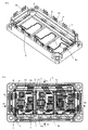
- FIG. 1 is a disassembled perspective view illustrating a part of the semiconductor module in which the semiconductor module is not assembled yet according to an embodiment of the present invention.
- FIG. 1a shows a perspective view of an upper lid 8.
- the upper lid 8 includes a partition 8b and a columnar part 8a.
- the partition 8b and the columnar part 8a are disposed to the upper lid 8 whose side faces to an insulating circuit board 9.
- the partition 8b presses a part of a crosspiece 5a of a resin frame body 5 shown in FIG. 1b .
- Each one of the columnar parts 8a presses each one of the insulating circuit boards 9 at respective center parts shown in FIG. 1c .
- FIG. 1b shows the resin frame body 5 in which metal terminals 4a and 4b are insert-molded in a frame element 5c.
- the resin frame body 5 includes the crosspiece 5a, the frame element 5c, and a stepped section 5e.
- An aperture 5b which is surrounded by the crosspiece 5a and the frame element 5c, has an open hole.
- the stepped section 5e is disposed along the inside wall of the resin frame body 5, and the upper face of the stepped section 5 forms a face on which the metal terminals 4a and 4b are disposed.
- the resin frame body 5 includes a through-hole 6 for fixing the semiconductor module to a heat sink not shown.
- a material for forming the resin frame body 5 and the upper lid 8 is preferably selected from a poly(phenylene sulfide) resin (PPS resin), a polyamide resin (PA resin), an acrylonitrile-butadiene-styrene resin (ABS resin), a poly(butylene terephthalate) resin, and the like.
- PPS resin poly(phenylene sulfide) resin
- PA resin polyamide resin
- ABS resin acrylonitrile-butadiene-styrene resin
- ABS resin poly(butylene terephthalate) resin
- FIG. 1c shows an insulating circuit board 9 in which semiconductor chips and bonding wires (conductive components) are omitted.
- Known insulating ceramics such as alumina, aluminum nitride, and silicon nitride can be employed for the insulating circuit board 9.
- a circuit pattern 9a having copper foil or the like is connected to each front surface of the insulating circuit boards 9, and the copper foil is connected to each entire back surface but periphery of the insulating circuit boards 9.
- semiconductor chips 2a and 2b such as an insulated gate bipolar transistor (IGBT) and a free-wheeling diode (FWD) are mounted so as to be joined with solder on the circuit pattern 9a.
- IGBT insulated gate bipolar transistor
- FWD free-wheeling diode
- FIG. 2 shows a perspective view in a state where the resin frame body 5 shown in FIG. 1b is mounted on the insulating circuit boards 9 shown in FIG. 1c .
- the metal terminals 4a and 4b are buried in the resin frame body 5.
- a leg 4c of the metal terminal is disposed on the upper face of the stepped section 5e so as to be extended from the resin frame body 5.
- the upper face of the stepped section 5e may be flat or may have recessed parts engaging the legs of the metal terminals 4a and 4b as shown in the figure. This can fix the metal terminals 4a and 4b surely and then prevent displacement.
- the size of the aperture 5b disposed at the center of the resin frame body 5 is formed slightly smaller than that of the insulating circuit board. Then the resin frame body 5 can press constantly to glue the periphery of the insulating circuit board 9.
- the crosspiece 5a of the resin frame body 5 presses to glue the insulating circuit boards 9 adjacent to each other in the vicinity of the outer edges.
- FIG. 3 show a top view illustrating a state where the resin frame body 5 has been mounted on the insulating circuit boards in which semiconductor chips have been mounted as shown in FIG. 2 , and then bonding wires (conductive components) 7 have been connected.
- the semiconductor chips 2a and 2b such as an IGBT and a FWD are connected to the circuit pattern 9a through solder.
- wire bonding lines 7a and 7b are applied for connection such as between the semiconductor chips 2a and 2b, between the insulating circuit boards, and between the insulating circuit board and the leg 4c of the metal terminal in order to constitute a desired inverter circuit and the like.
- the bonding wire 7, striding over the crosspiece 5a of the resin frame body 5, is applied on the faces between the circuit patterns 9a, so this achieves the connection electrically between the insulating circuit boards 9 being adjacent to each other.
- the conductive components are not limited to the bonding wire described above and then may be a flat plate-like material.
- FIG. 4 shows an outline cross section view adding a cross section view of the upper lid 8 to a cross section view cut along the line B1-B2 in FIG. 3 .
- the semiconductor chips and the bonding wires 7a and 7b, and the like are omitted to be recognized easily.
- Each one of the metal terminals 4a and 4b includes a shaft 4d, the leg 4c, and a hinge portion 4e, which is bent, coupling the shaft 4d to the leg 4c.
- the hinge portion 4e has a narrower width than the shaft 4d or the leg 4c and engages with the resin frame body.
- the leg 4c bent from the hinge portion 4e is fixed to the stepped section 5e. Then this can suppress displacement between the metal terminal 4a or 4b and the resin frame body 5.
- the metal terminals 4a and 4b according to the present invention have a shape narrower in width of the hinge portion 4e engaging with the resin frame body 5 than in that of the shaft 4d or the leg 4c. Then when the metal terminals are manufactured by press working, a layout has been realized with a narrower pitch, and then timber offcuts decrease in quantity. Thus this can increase the production number of metal terminals per unit area.
- the semiconductor module illustrated in the cross section view of FIG. 4 holds the metal terminals 4a and 4b which are molded integrally in a state where each part of the legs 4c of the metal terminals 4a and 4b is exposed on the flat upper face of the stepped section 5e which is located inside the resin frame body 5, and each part of the shafts 4d is led outside.
- the metal terminals 4a and 4b may not be necessarily molded integrally into the resin frame body 5.
- the metal terminals may be inserted integrally by engaging with a molded resin frame body.
- the metal terminals 4a and 4b are collected to the resin frame body 5 locating outside the area where wire bonding lines are formed, and then only the legs 4c which are bent in an L-shape at the hinge portion are exposed on the stepped section 5e inside the resin frame body 5. Then the shafts 4d of the metal terminals are buried in the resin frame body 5, and only the legs of the metal terminals which become points connecting bonding wires are exposed on the other hand. Then this can render wire bonding operation easier and achieve connection with higher reliability.
- FIG. 5 shows an outline cross section view cut along the line B1-B2 in a state where the upper lid 8 shown in FIG. 4 is set to a proper position.
- the semiconductor chips, the bonding wires 7a and 7b around the chips, and the like are omitted as similar to FIG.4 .
- the partition 8b and the columnar part 8a are provided on the lower side of the upper lid 8.
- the partition 8b is disposed so as to press the upper face of the crosspiece 5a provided in the resin frame body 5 when an opening disposed at an upper part of the resin frame body 5 is covered with the upper lid 8.
- the columnar part 8a is disposed so that the insulating circuit board 9 is pressed near the central part.
- the bonding wire 7 strides over the crosspiece 5a of the resin frame body 5 and achieves connection. Then if the bottom face of the partition 8b is set to the same dimension as the top face of the crosspiece 5a, the partition 8b shall interfere with the bonding wire 7. Then the present invention has a feature that the partition 8b disposed on the upper lid 8 has a figure avoiding interference with the bonding wire 7. As the bonding wires 7 are, for example, shown in FIG.
- the partition 8b is formed to have the figure that the partition 8b is in contact with the crosspiece 5a at only a part of the top face interposed between the bonding wires 7 so that the partition 8b avoids being in contact with the bonding wire 7.
- the partition 8b presses the insulating circuit board 9 through the crosspiece 5a.
- each peripheral edge of insulating circuit boards 9 will be equally in contact with the crosspiece 5a and the frame element 5c which are outer peripheries of the resin frame body 5. Then this can provide pressure force almost uniformly toward the insulating circuit boards 9.
- the plurality of insulating circuit boards 9 glues the frame element 5c and the crosspieces 5a on the lower faces with adhesion material in the resin frame body 5. As a result, this can suppress warpage deformation of the insulating circuit board 9 in a semiconductor module 1.
- the semiconductor module 1 comprises the plurality of insulating circuit boards 9 which are adjacent to each other and arranged in line, the resin frame body 5 glued on the periphery of the insulating circuit boards 9, and the upper lid 8 which closes the opening disposed at an upper side of the resin frame body 5.
- a method that the upper lid 8 covers the opening disposed at the upper part of the resin frame body 5 may be performed so that the resin frame body 5 is glued with adhesion material. Further, another method may be performed so as to provide an engagement portion where the upper lid 8 is fixed to the resin frame body 5.
- the engagement portion may have a structure such as interlocking, a screw stopper, or mesh. This can ensure that the pressure force is provided from the columnar part 8a and the partition 8b disposed on the upper lid 8 toward the insulating circuit board 9.
- a method for manufacturing the semiconductor module 1 comprises the steps of disposing the insulating circuit boards 9 and the resin frame body 5 so that the crosspiece 5a is disposed on first outer edges of the insulating circuit boards 9 which are opposed to each other, and the frame element 5c of the resin frame body 5 is disposed on second outer edges of the plurality of insulating circuit boards 9 in a first step, achieving the connection between the insulating circuit boards 9 electrically with the conductive components 7 so as to stride over the crosspiece 5a in a second step, and fixing the upper lid 8 to the resin frame body 5 so that the lid element 8c of the upper lid 8 covers the opening disposing at the upper part of the resin frame body, and the partition 8b disposed on the upper lid 8 abuts on a part of the crosspiece 5a in a third step.
- silicone gel or the like is injected to seal the inside empty space surrounded by the resin frame body
- the semiconductor module has the structure with the plurality of insulating circuit boards, there is provided the semiconductor module which enables to achieve easily the connection between the insulating circuit boards electrically and to radiate heat produced from the semiconductor chips efficiently under suppression of warpage deformation of the insulating circuit boards.
Landscapes
- Engineering & Computer Science (AREA)
- Manufacturing & Machinery (AREA)
- Microelectronics & Electronic Packaging (AREA)
- Structures Or Materials For Encapsulating Or Coating Semiconductor Devices Or Solid State Devices (AREA)
- Inverter Devices (AREA)
- Physics & Mathematics (AREA)
- Geometry (AREA)
- Chemical & Material Sciences (AREA)
- Dispersion Chemistry (AREA)
Abstract
Description
- The invention relates to a semiconductor module that accommodates a circuit formed by using a plurality of insulating circuit boards in a case with a lid.
- A structure that a shielding plate is disposed at the center portion of one board accommodated in a case is known in
Patent Literature 1. The following descriptions are referred in Patent literature 1: an optical receiving IC and an amplifier IC are mounted on one board, which has right and left notches at the center section between the optical receiving IC and the amplifier IC; a notch is formed at the bottom face of the shielding plate in which the face will be opposed to a signal line in order to avoid abutting on the signal line provided on the board; and the shielding plate is inserted so as to be engaged with the board through the whole thickness at the notch parts. A lid is disposed on the case and the shielding plate. - Further, a power semiconductor module is described in Patent literature 2: a protrusion is disposed on the back side of a lid plate to press a control circuit printed board from the upper side, and then this suppresses the printed board from shifting up and relaxes a stress generated in a solder joined part where a lead pin is connected to the printed board.
- Moreover, as a reference of a terminal, a semiconductor module including a plurality of semiconductor chips, bonding wires, a resin case, and external lead-out metal terminals (hereinafter, metal terminals), which are insert-molded in the resin case, is described in Patent literature 3. The metal terminals are insert-molded at an outer peripheral frame of the resin case to enlarge an inside space of the case, and wiring is carried out by using only bonding wires between two parts such as an insulating circuit board, a semiconductor chip and a terminal. Then the metal terminal is not joined directly with solder on the insulating circuit board in the structure. The structure demands that the metal terminal is surely fixed with the resin case. If the metal terminal hangs on the resin case, connection failure may occur when wire bonding is performed to the metal terminal. Then in conventional arts, immobility between the metal terminal and the resin case has been strengthened so that convex parts protruding outside are provided at the bottom part of the metal terminal bent in an L-shape, and the corresponding part of the resin case is formed in a step-wise in order to support the metal terminal surely at the bottom part where wire bonding is performed.
-
- Patent Literature 1: Japanese Patent Application Laid-open No.
2005-50974 - Patent Literature 2:
JP-A No. 2000-68446 - Patent Literature 3:
JP-A No. 2000-208655 - In a semiconductor module employing one sheet of insulating circuit board, an area necessary for the insulating circuit board increases when a semiconductor chip becomes bigger in size, and the number of chips increases further. If the insulating circuit board area increases excessively, warp and crack might occur in the insulating circuit board owing to stress caused by the difference in coefficients of thermal expansion. Then, in the case that the insulating circuit board becomes bigger further, it is available that the one sheet of insulating circuit board is divided into a plurality of insulating circuit boards, which are assembled to make another structure, for the sake of decreasing effect of warp coming from the insulating circuit boards to improve adhesion between the insulating circuit boards and a heat sink. However, there is no description in the above references about a semiconductor module that a plurality of insulating circuit boards, which form a circuit, are accommodated in a case with a lid, and each one of all peripheries of the plurality of insulating circuit boards is pressed and then fixed from the upper side. As shown in
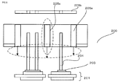
FIG. 6 , if a structure has not just an outer frame of aresin case 205a but also awall 205c, which is disposed around the center part, holding a periphery ofinsulating circuit boards 201, there is a problem that connection betweeninsulating circuit boards 201 cannot be performed by using bonding wires because thewall 205c becomes a barrier. - Furthermore, in the case that the metal terminal has convex parts outside as described above in Patent literature 3, there is a problem that the production number of metal terminals per unit area of a metal plate decreases when the metal terminals are manufactured from the metal plate being raw material.
- In view of the problems mentioned above, it is an object of the present invention to provide a semiconductor module that can readily achieve connection between insulating circuit boards electrically and suppress warpage deformation to radiate heat produced from semiconductor chips efficiently, even though the structure is formed so as to have the plurality of insulating circuit boards.
- In order to solve the problem described above and to attain the object of the invention, according to an aspect of the invention, there is provided a semiconductor module comprising a plurality of insulating circuit boards which include semiconductor chips; a resin frame body which has a crosspiece abutting on first outer edges of the insulating circuit boards in which a first outer edge among the outer edges thereof is opposed to the adjacent insulating circuit board and a frame element abutting on second outer edges which exclude the first outer edges from the outer edges of the insulating circuit boards; a conductive component which achieves connection between the insulating circuit boards electrically so that the conductive component strides over the crosspiece; and an upper lid which has a lid element covering an opening disposed at an upper part of the resin frame body and a partition protruding from the lid element whose face is opposed to the circuit boards and abutting on a part of the crosspiece.
- According to the above aspect of the invention, without being obstructed by the partition, the conductive component can stride over the crosspiece to achieve the connection between the insulating circuit boards electrically. Further, the partition disposed on the upper lid can press the crosspiece of the resin frame body, and then the crosspiece can press the first outer edges of the insulating circuit boards. Thus this can suppress the insulating circuit board from warping.
- In the semiconductor module according to the above aspect of the invention, the upper lid preferably includes a columnar part which abuts on the insulating circuit board, wherein the columnar part protrudes from the lid element whose face is opposed to the insulating circuit boards.
- According to the constitution described above, the columnar part of the upper lid can press the center portion of the insulating circuit board. Then this can suppress the insulating circuit board from warping. In addition, the upper lid may be glued to the resin frame body, so the upper lid can be easily attached to the resin frame body. Moreover, another constitution may also have an engagement portion which can fix the upper lid to the resin frame body, so the upper lid can be easily attached to the resin frame body further.
- In the semiconductor module according to the above aspect of the invention, the resin frame body preferably includes a stepped section disposed along an inside wall of the resin frame body, and a metal terminal which has a shaft, a leg, and a hinge portion, which is bent, coupling the shaft to the leg with narrower width than the shaft or the leg, wherein the leg is preferably disposed on the upper face of the stepped section.
- According to the constitution described above, the hinge portion is formed narrower in width than either at least one of the shaft and leg or both of them, being engaged to the resin frame body. Then the leg bent from the hinge portion can be fixed on the upper face of the stepped section. Then this can suppress displacement between the metal terminal and the resin frame body. Furthermore, the hinge portion of the metal terminal, which engages the resin frame body, has a shape narrower than the overall width of the metal terminal. Then when the metal terminals are manufactured by press working, a layout has been realized with a narrower pitch, and then timber offcuts decrease in quantity. Thus this can increase the production number of metal terminals per unit area.
- In the semiconductor module according to the above aspect of the present invention, in a state where a part of the shaft and a part of the leg are exposed, the metal terminal is preferably buried in the frame element of the resin frame body.
- According to the constitution described above, the shaft of the metal terminal can be buried in the resin frame body, and only the leg of the metal terminal, which become a point connecting a bonding wire, can be exposed. Then wire bonding operation can be performed easily. Then this can result in connection having high reliability.
- According to another aspect of the invention, there is provided a method for manufacturing a semiconductor module, wherein the semiconductor module comprises a plurality of insulating circuit boards which include semiconductor chips, a resin frame body which has a crosspiece abutting on first outer edges of the insulating circuit boards in which a first outer edge among outer edges thereof is opposed to the adjacent insulating circuit board and a frame element abutting on second outer edges which exclude the first outer edges from the outer edges of the insulating circuit boards, a conductive component which achieves connection between the insulating circuit boards electrically so that the conductive component strides over the crosspiece, and an upper lid which has a lid element covering an opening disposed at an upper part of the resin frame body and a partition protruding from the lid element whose face is opposed to the insulating circuit boards and abutting on a part of the crosspiece, comprising the steps of disposing the insulating circuit boards and the resin frame body so that the crosspiece abuts on the first outer edges, and the frame element abuts on the second outer edges in a first step, achieving the connection between the insulating circuit boards electrically with the conductive component so that the conductive component strides over the crosspiece in a second step, and fixing the upper lid to the resin frame body so that the lid element of the upper lid covers the opening disposed at the upper part of the resin frame body, and the partition disposed on the upper lid abuts on a part of the crosspiece in a third step.
- According to the above aspect of the invention, without being obstructed by the partition, the conductive component can stride over the crosspiece to achieve the connection between the insulating circuit boards electrically.
- According to the present invention, even though a semiconductor module has a structure with a plurality of insulating circuit boards, it is possible to provide the semiconductor module which can achieve the connection electrically between the insulating circuit boards easily and suppress the insulating circuit boards from warpage deformation to radiate heat produced from semiconductor chips efficiently.
-
-
FIG. 1 is a disassembled perspective view of a semiconductor module in which the semiconductor module is not assembled yet according to an embodiment of the present invention. -
FIG. 2 illustrates a disassembled perspective view in a state where aresin frame body 5 shown inFIG. 1b is mounted oninsulating circuit boards 9 shown inFIG. 1c . -
FIG. 3 is a top view illustrating a state where theresin frame body 5 has been mounted on the insulating circuit boards in which semiconductor chips have been mounted as shown inFIG. 2 , and then bonding wires (conductive components) 7 have been connected. -
FIG. 4 is an outline cross section view adding a cross section view of anupper lid 8 to a cross section view cut along the line B1-B2 inFIG. 3 . Semiconductor chips andbonding wires 7a and 7b around the chips, and the like are omitted to be recognized easily. -
FIG. 5 shows an outline cross section view cut along the line B1-B2 in a state where theupper lid 8 is set to a proper position. As similar toFIG.4 , the semiconductor chips and thebonding wires 7a and 7b around the chips, and the like are omitted. -
FIG.6 is a schematic cross section view illustrating an outline structure of a conventional semiconductor module employing a plurality of insulating circuit boards. - Hereinafter, preferred embodiments of a semiconductor module according to the invention will be described in detail with reference to the accompanying drawings. In addition, in the following description of the embodiments and accompanying drawings, the same constituent elements will be denoted by the same reference numerals, and redundant descriptions thereof will be omitted. Furthermore, the accompanying figures described in the embodiments are not drawn by using accurate scale and proportion for the sake of being easily recognized or surely understood. The invention is not limited to the details of the embodiments described hereinafter, provided that it does not exceed the gist thereof.
-
FIG. 1 is a disassembled perspective view illustrating a part of the semiconductor module in which the semiconductor module is not assembled yet according to an embodiment of the present invention. -
FIG. 1a shows a perspective view of anupper lid 8. Theupper lid 8 includes apartition 8b and acolumnar part 8a. Thepartition 8b and thecolumnar part 8a are disposed to theupper lid 8 whose side faces to an insulatingcircuit board 9. Thepartition 8b presses a part of acrosspiece 5a of aresin frame body 5 shown inFIG. 1b . Each one of thecolumnar parts 8a presses each one of the insulatingcircuit boards 9 at respective center parts shown inFIG. 1c . -
FIG. 1b shows theresin frame body 5 in whichmetal terminals frame element 5c. Theresin frame body 5 includes thecrosspiece 5a, theframe element 5c, and a steppedsection 5e. Anaperture 5b, which is surrounded by thecrosspiece 5a and theframe element 5c, has an open hole. The steppedsection 5e is disposed along the inside wall of theresin frame body 5, and the upper face of the steppedsection 5 forms a face on which themetal terminals resin frame body 5 includes a through-hole 6 for fixing the semiconductor module to a heat sink not shown. A material for forming theresin frame body 5 and theupper lid 8 is preferably selected from a poly(phenylene sulfide) resin (PPS resin), a polyamide resin (PA resin), an acrylonitrile-butadiene-styrene resin (ABS resin), a poly(butylene terephthalate) resin, and the like. -
FIG. 1c shows an insulatingcircuit board 9 in which semiconductor chips and bonding wires (conductive components) are omitted. Known insulating ceramics such as alumina, aluminum nitride, and silicon nitride can be employed for the insulatingcircuit board 9. Acircuit pattern 9a having copper foil or the like is connected to each front surface of the insulatingcircuit boards 9, and the copper foil is connected to each entire back surface but periphery of the insulatingcircuit boards 9. As shown inFIG. 3 described later, semiconductor chips 2a and 2b such as an insulated gate bipolar transistor (IGBT) and a free-wheeling diode (FWD) are mounted so as to be joined with solder on thecircuit pattern 9a. -
FIG. 2 shows a perspective view in a state where theresin frame body 5 shown inFIG. 1b is mounted on the insulatingcircuit boards 9 shown inFIG. 1c . Themetal terminals resin frame body 5. Aleg 4c of the metal terminal is disposed on the upper face of the steppedsection 5e so as to be extended from theresin frame body 5. The upper face of the steppedsection 5e may be flat or may have recessed parts engaging the legs of themetal terminals metal terminals aperture 5b disposed at the center of theresin frame body 5 is formed slightly smaller than that of the insulating circuit board. Then theresin frame body 5 can press constantly to glue the periphery of the insulatingcircuit board 9. Thecrosspiece 5a of theresin frame body 5 presses to glue the insulatingcircuit boards 9 adjacent to each other in the vicinity of the outer edges. -
FIG. 3 show a top view illustrating a state where theresin frame body 5 has been mounted on the insulating circuit boards in which semiconductor chips have been mounted as shown inFIG. 2 , and then bonding wires (conductive components) 7 have been connected. The semiconductor chips 2a and 2b such as an IGBT and a FWD are connected to thecircuit pattern 9a through solder. Then,wire bonding lines 7a and 7b are applied for connection such as between the semiconductor chips 2a and 2b, between the insulating circuit boards, and between the insulating circuit board and theleg 4c of the metal terminal in order to constitute a desired inverter circuit and the like. Further thebonding wire 7, striding over thecrosspiece 5a of theresin frame body 5, is applied on the faces between thecircuit patterns 9a, so this achieves the connection electrically between the insulatingcircuit boards 9 being adjacent to each other. In addition, the conductive components are not limited to the bonding wire described above and then may be a flat plate-like material. -
FIG. 4 shows an outline cross section view adding a cross section view of theupper lid 8 to a cross section view cut along the line B1-B2 inFIG. 3 . The semiconductor chips and thebonding wires 7a and 7b, and the like are omitted to be recognized easily. Each one of themetal terminals shaft 4d, theleg 4c, and a hinge portion 4e, which is bent, coupling theshaft 4d to theleg 4c. The hinge portion 4e has a narrower width than theshaft 4d or theleg 4c and engages with the resin frame body. Theleg 4c bent from the hinge portion 4e is fixed to the steppedsection 5e. Then this can suppress displacement between themetal terminal resin frame body 5. - In addition, the
metal terminals resin frame body 5 than in that of theshaft 4d or theleg 4c. Then when the metal terminals are manufactured by press working, a layout has been realized with a narrower pitch, and then timber offcuts decrease in quantity. Thus this can increase the production number of metal terminals per unit area. - The semiconductor module illustrated in the cross section view of
FIG. 4 holds themetal terminals legs 4c of themetal terminals section 5e which is located inside theresin frame body 5, and each part of theshafts 4d is led outside. However, themetal terminals resin frame body 5. The metal terminals may be inserted integrally by engaging with a molded resin frame body. As mentioned above, themetal terminals resin frame body 5 locating outside the area where wire bonding lines are formed, and then only thelegs 4c which are bent in an L-shape at the hinge portion are exposed on the steppedsection 5e inside theresin frame body 5. Then theshafts 4d of the metal terminals are buried in theresin frame body 5, and only the legs of the metal terminals which become points connecting bonding wires are exposed on the other hand. Then this can render wire bonding operation easier and achieve connection with higher reliability. -
FIG. 5 shows an outline cross section view cut along the line B1-B2 in a state where theupper lid 8 shown inFIG. 4 is set to a proper position. The semiconductor chips, thebonding wires 7a and 7b around the chips, and the like are omitted as similar toFIG.4 . As shown inFIG. 1a using a broken line, thepartition 8b and thecolumnar part 8a are provided on the lower side of theupper lid 8. As shown inFIGS. 4 and 5 , thepartition 8b is disposed so as to press the upper face of thecrosspiece 5a provided in theresin frame body 5 when an opening disposed at an upper part of theresin frame body 5 is covered with theupper lid 8. Thecolumnar part 8a is disposed so that the insulatingcircuit board 9 is pressed near the central part. - However, as described earlier, there is a place where the
bonding wire 7 strides over thecrosspiece 5a of theresin frame body 5 and achieves connection. Then if the bottom face of thepartition 8b is set to the same dimension as the top face of thecrosspiece 5a, thepartition 8b shall interfere with thebonding wire 7. Then the present invention has a feature that thepartition 8b disposed on theupper lid 8 has a figure avoiding interference with thebonding wire 7. As thebonding wires 7 are, for example, shown inFIG. 3 , if thebonding wires 7 are disposed at positions being in the vicinity of both edges of the insulatingcircuit boards 9, thepartition 8b is formed to have the figure that thepartition 8b is in contact with thecrosspiece 5a at only a part of the top face interposed between thebonding wires 7 so that thepartition 8b avoids being in contact with thebonding wire 7. As mentioned above, even though the dimension of thepartition 8b is formed to be shorter in shape than that of thecrosspiece 5a positioning at the lower side so as not to be in contact with thebonding wire 7, thepartition 8b presses the insulatingcircuit board 9 through thecrosspiece 5a. Then, with regard to the plurality of insulatingcircuit boards 9, each peripheral edge of insulatingcircuit boards 9 will be equally in contact with thecrosspiece 5a and theframe element 5c which are outer peripheries of theresin frame body 5. Then this can provide pressure force almost uniformly toward the insulatingcircuit boards 9. The plurality of insulatingcircuit boards 9 glues theframe element 5c and thecrosspieces 5a on the lower faces with adhesion material in theresin frame body 5. As a result, this can suppress warpage deformation of the insulatingcircuit board 9 in asemiconductor module 1. A heat sink, in which a face opposed to the back face of the insulatingcircuit board 9 is formed so as to have a flat surface, is in contact with each backside copper foil of the plurality of insulatingcircuit boards 9. Screw grooves are formed in the flat surface, and then theresin frame body 5 is fixed to the heat sink with screws threading through the through-hole 6. Therefore it is possible to radiate heat produced from the semiconductor chips 2a and 2b to the heat sink not shown. Further with regard to theupper lid 8, thepartition 8b presses the insulatingcircuit board 9 through thecrosspiece 5a. Then the length of thepartition 8b determined from theupper lid 8 will become shorter than that of thecolumnar part 8a determined from theupper lid 8. This also provides a feature in structure of one aspect of the embodiment described above. - As shown in the perspective views of
FIGS. 1 and2 and in the top view ofFIG. 3 , thesemiconductor module 1 according to the present invention comprises the plurality of insulatingcircuit boards 9 which are adjacent to each other and arranged in line, theresin frame body 5 glued on the periphery of the insulatingcircuit boards 9, and theupper lid 8 which closes the opening disposed at an upper side of theresin frame body 5. A method that theupper lid 8 covers the opening disposed at the upper part of theresin frame body 5 may be performed so that theresin frame body 5 is glued with adhesion material. Further, another method may be performed so as to provide an engagement portion where theupper lid 8 is fixed to theresin frame body 5. The engagement portion may have a structure such as interlocking, a screw stopper, or mesh. This can ensure that the pressure force is provided from thecolumnar part 8a and thepartition 8b disposed on theupper lid 8 toward the insulatingcircuit board 9. - A method for manufacturing the
semiconductor module 1 according to the present invention comprises the steps of disposing the insulatingcircuit boards 9 and theresin frame body 5 so that thecrosspiece 5a is disposed on first outer edges of the insulatingcircuit boards 9 which are opposed to each other, and theframe element 5c of theresin frame body 5 is disposed on second outer edges of the plurality of insulatingcircuit boards 9 in a first step, achieving the connection between the insulatingcircuit boards 9 electrically with theconductive components 7 so as to stride over thecrosspiece 5a in a second step, and fixing theupper lid 8 to theresin frame body 5 so that the lid element 8c of theupper lid 8 covers the opening disposing at the upper part of the resin frame body, and thepartition 8b disposed on theupper lid 8 abuts on a part of thecrosspiece 5a in a third step. Before theupper lid 8 has covered theresin frame body 5 in the third step, it is more preferable to include a fourth step that silicone gel or the like is injected to seal the inside empty space surrounded by theresin frame body 5 and the insulatingcircuit boards 9. - As mentioned above, according to the embodiment of the present invention, even though the semiconductor module has the structure with the plurality of insulating circuit boards, there is provided the semiconductor module which enables to achieve easily the connection between the insulating circuit boards electrically and to radiate heat produced from the semiconductor chips efficiently under suppression of warpage deformation of the insulating circuit boards.
-
- 1: semiconductor module
- 2a, 2b: semiconductor chip
- 4a, 4b: metal terminal
- 4c: leg of metal terminal
- 4d: shaft of metal terminal
- 4e: hinge portion of metal terminal
- 5: resin frame body
- 5a: crosspiece
- 5b: aperture
- 5c: frame element
- 5d: engagement portion located at resin frame body side
- 5e: stepped section
- 6: through-hole
- 7, 7a: bonding wire (conductive component)
- 8: upper lid
- 8a: columnar part
- 8b: partition
- 8c: lid element
- 8d: engagement portion located at upper lid side
- 9: insulating circuit board
- 9a: circuit pattern
- 200: semiconductor module
- 201: insulating circuit board
- 203: semiconductor chip
- 204: external lead-out metal terminal
- 205a: resin case
- 205b: upper lid
- 205c: wall
Claims (5)
- A semiconductor module comprising:a plurality of insulating circuit boards which include semiconductor chips;a resin frame body which has a crosspiece abutting on first outer edges of the insulating circuit boards in which a first outer edge among the outer edges thereof is opposed to the adjacent insulating circuit board and a frame element abutting on second outer edges which exclude the first outer edges from the outer edges of the insulating circuit boards;a conductive component which achieves connection between the insulating circuit boards electrically so that the conductive component strides over the crosspiece; andan upper lid which has a lid element covering an opening disposed at an upper part of the resin frame body and a partition protruding from the lid element whose face is opposed to the circuit boards and abutting on a part of the crosspiece.
- The semiconductor module according to claim 1, wherein the upper lid includes a columnar part which abuts on an insulating circuit board, wherein the columnar part protrudes from the lid element whose face is opposed to the insulating circuit boards.
- The semiconductor module according to claim 1 or 2,
wherein the resin frame body includes a stepped section disposed along an inside wall of the resin frame body, and
a metal terminal which has a shaft, a leg, and a hinge portion, which is bent, coupling the shaft to the leg with a narrower width than the shaft or the leg,
wherein the leg is disposed on the upper face of the stepped section. - The semiconductor module according to any one of claims 1 to 3, wherein in a state where a part of the shaft and a part of the leg are exposed, the metal terminal is buried in the frame element of the resin frame body.
- A method for manufacturing a semiconductor module, wherein the semiconductor module comprises a plurality of insulating circuit boards which include semiconductor chips, a resin frame body which has a crosspiece abutting on first outer edges of the insulating circuit boards in which a first outer edge among outer edges thereof is opposed to the adjacent insulating circuit board and a frame element abutting on second outer edges which exclude the first outer edges from the outer edges of the insulating circuit boards, a conductive component which achieves connection between the insulating circuit boards electrically so that the conductive component strides over the crosspiece, and an upper lid which has a lid element covering an opening disposed at an upper part of the resin frame body and a partition protruding from the lid element whose face is opposed to the insulating circuit boards and abutting on a part of the crosspiece, comprising the steps of:disposing the insulating circuit boards and the resin frame body so that the crosspiece abuts on the first outer edges, and the frame element abuts on the second outer edges in a first step;achieving the connection between the insulating circuit boards electrically with the conductive component so that the conductive component strides over the crosspiece in a second step; andfixing the upper lid to the resin frame body so that the lid element of the upper lid covers the opening disposed at the upper part of the resin frame body, and the partition disposed on the upper lid abuts on a part of the crosspiece in a third step.
Applications Claiming Priority (2)
| Application Number | Priority Date | Filing Date | Title |
|---|---|---|---|
| JP2014006436 | 2014-01-17 | ||
| PCT/JP2014/082632 WO2015107804A1 (en) | 2014-01-17 | 2014-12-10 | Semiconductor module |
Publications (3)
| Publication Number | Publication Date |
|---|---|
| EP3007219A1 true EP3007219A1 (en) | 2016-04-13 |
| EP3007219A4 EP3007219A4 (en) | 2017-02-22 |
| EP3007219B1 EP3007219B1 (en) | 2020-02-12 |
Family
ID=53542708
Family Applications (1)
| Application Number | Title | Priority Date | Filing Date |
|---|---|---|---|
| EP14879151.0A Active EP3007219B1 (en) | 2014-01-17 | 2014-12-10 | Semiconductor module |
Country Status (5)
| Country | Link |
|---|---|
| US (1) | US9673117B2 (en) |
| EP (1) | EP3007219B1 (en) |
| JP (1) | JP6132034B2 (en) |
| CN (1) | CN105940489B (en) |
| WO (1) | WO2015107804A1 (en) |
Families Citing this family (7)
| Publication number | Priority date | Publication date | Assignee | Title |
|---|---|---|---|---|
| JP6523976B2 (en) * | 2016-01-15 | 2019-06-05 | 京セラ株式会社 | Semiconductor device |
| JPWO2017163638A1 (en) * | 2016-03-22 | 2018-06-14 | 富士電機株式会社 | CASE, SEMICONDUCTOR DEVICE, AND CASE MANUFACTURING METHOD |
| JP6810601B2 (en) * | 2016-12-26 | 2021-01-06 | 新電元工業株式会社 | Manufacturing method of electronic device |
| EP3682475A1 (en) | 2017-09-15 | 2020-07-22 | Finar Module Sagl | Packaging method and joint technology for an electronic device |
| JP6848802B2 (en) * | 2017-10-11 | 2021-03-24 | 三菱電機株式会社 | Semiconductor device |
| JP6594556B1 (en) | 2018-01-17 | 2019-10-23 | 新電元工業株式会社 | Electronic module |
| CN110060986B (en) * | 2019-05-06 | 2021-09-14 | 如皋市大昌电子有限公司 | Axial array type rectifier bridge stack |
Family Cites Families (17)
| Publication number | Priority date | Publication date | Assignee | Title |
|---|---|---|---|---|
| US4908738A (en) * | 1986-12-19 | 1990-03-13 | Fanuc Ltd | Drive motor control unit |
| JPH1093016A (en) * | 1996-09-19 | 1998-04-10 | Hitachi Ltd | Power semiconductor device |
| JP2000068446A (en) | 1998-08-25 | 2000-03-03 | Hitachi Ltd | Power semiconductor module |
| JP3671712B2 (en) | 1999-01-11 | 2005-07-13 | 富士電機デバイステクノロジー株式会社 | Electronic component built-in module |
| JP3808050B2 (en) * | 2003-03-17 | 2006-08-09 | Tdk株式会社 | Surface mount package and electronic component using the same |
| JP2005050974A (en) | 2003-07-31 | 2005-02-24 | Toshiba Corp | Semiconductor package, optical communication module, and semiconductor device |
| JP2005123219A (en) * | 2003-10-14 | 2005-05-12 | Nissan Motor Co Ltd | Semiconductor device |
| JP4434879B2 (en) * | 2004-08-24 | 2010-03-17 | 三菱電機株式会社 | Power semiconductor device |
| KR100691629B1 (en) * | 2006-04-21 | 2007-03-12 | 삼성전기주식회사 | High frequency module using metal wall and manufacturing method thereof |
| JP5041798B2 (en) * | 2006-12-15 | 2012-10-03 | 三菱電機株式会社 | Semiconductor device |
| US7944042B2 (en) | 2007-03-08 | 2011-05-17 | Fuji Electric Device Technology Co., Ltd. | Semiconductor device and method of manufacturing same |
| JP4985116B2 (en) * | 2007-03-08 | 2012-07-25 | 富士電機株式会社 | Semiconductor device and manufacturing method thereof |
| US8237260B2 (en) * | 2008-11-26 | 2012-08-07 | Infineon Technologies Ag | Power semiconductor module with segmented base plate |
| JP2011199213A (en) * | 2010-03-24 | 2011-10-06 | Daikin Industries Ltd | Power module |
| KR101719644B1 (en) * | 2010-05-24 | 2017-04-04 | 서울반도체 주식회사 | Light emitting diode package |
| US9153512B2 (en) * | 2011-04-22 | 2015-10-06 | Mitsubishi Electric Corporation | Semiconductor device with an insulating terminal table |
| JP5466785B1 (en) * | 2013-08-12 | 2014-04-09 | 太陽誘電株式会社 | Circuit module and manufacturing method thereof |
-
2014
- 2014-12-10 EP EP14879151.0A patent/EP3007219B1/en active Active
- 2014-12-10 JP JP2015557735A patent/JP6132034B2/en active Active
- 2014-12-10 WO PCT/JP2014/082632 patent/WO2015107804A1/en not_active Ceased
- 2014-12-10 CN CN201480038707.XA patent/CN105940489B/en active Active
-
2016
- 2016-01-07 US US14/990,423 patent/US9673117B2/en active Active
Non-Patent Citations (1)
| Title |
|---|
| See references of WO2015107804A1 * |
Also Published As
| Publication number | Publication date |
|---|---|
| EP3007219B1 (en) | 2020-02-12 |
| CN105940489B (en) | 2019-04-05 |
| WO2015107804A1 (en) | 2015-07-23 |
| US20160118310A1 (en) | 2016-04-28 |
| JP6132034B2 (en) | 2017-05-24 |
| JPWO2015107804A1 (en) | 2017-03-23 |
| US9673117B2 (en) | 2017-06-06 |
| EP3007219A4 (en) | 2017-02-22 |
| CN105940489A (en) | 2016-09-14 |
Similar Documents
| Publication | Publication Date | Title |
|---|---|---|
| EP3007219B1 (en) | Semiconductor module | |
| EP3226292B1 (en) | Lead frame, semiconductor device, method for manufacturing lead frame, and method for manufacturing semiconductor device | |
| US9848518B2 (en) | Integrated power module packaging structure | |
| US9603291B2 (en) | Semiconductor device | |
| EP2858109B1 (en) | Semiconductor module and semiconductor module manufacturing method | |
| US20140167237A1 (en) | Power module package | |
| JP6119313B2 (en) | Semiconductor device | |
| US20140160691A1 (en) | Semiconductor module and method of manufacturing the same | |
| US9806010B2 (en) | Package module and method of fabricating the same | |
| US20140231975A1 (en) | Semiconductor device | |
| EP3098843A1 (en) | Package assembly | |
| US9620438B2 (en) | Electronic device with heat dissipater | |
| US20180310410A1 (en) | Circuit assembly | |
| CN104600051B (en) | Semiconductor module | |
| WO2013145532A1 (en) | Resin package | |
| JP2014103270A (en) | Semiconductor module | |
| JP2004153243A (en) | Power semiconductor device | |
| JP7548089B2 (en) | Circuit device | |
| JP6831624B2 (en) | LED light emitting device | |
| US20120146208A1 (en) | Semiconductor module and manufacturing method thereof | |
| KR102185064B1 (en) | Power module and manufacturing method thereof | |
| KR20160051513A (en) | Power module and manufacturing method thereof | |
| CN113013129A (en) | Power module | |
| JP2001077508A (en) | Printed wiring board for mounting semiconductor element and manufacture thereof |
Legal Events
| Date | Code | Title | Description |
|---|---|---|---|
| PUAI | Public reference made under article 153(3) epc to a published international application that has entered the european phase |
Free format text: ORIGINAL CODE: 0009012 |
|
| 17P | Request for examination filed |
Effective date: 20160107 |
|
| AK | Designated contracting states |
Kind code of ref document: A1 Designated state(s): AL AT BE BG CH CY CZ DE DK EE ES FI FR GB GR HR HU IE IS IT LI LT LU LV MC MK MT NL NO PL PT RO RS SE SI SK SM TR |
|
| AX | Request for extension of the european patent |
Extension state: BA ME |
|
| A4 | Supplementary search report drawn up and despatched |
Effective date: 20170124 |
|
| RIC1 | Information provided on ipc code assigned before grant |
Ipc: H01L 25/18 20060101ALI20170118BHEP Ipc: H01L 23/053 20060101ALI20170118BHEP Ipc: H01L 25/07 20060101AFI20170118BHEP |
|
| DAX | Request for extension of the european patent (deleted) | ||
| REG | Reference to a national code |
Ref country code: DE Ref legal event code: R079 Ref document number: 602014061072 Country of ref document: DE Free format text: PREVIOUS MAIN CLASS: H01L0023020000 Ipc: H01L0025070000 |
|
| RIC1 | Information provided on ipc code assigned before grant |
Ipc: H01L 25/07 20060101AFI20190508BHEP Ipc: H01L 25/18 20060101ALI20190508BHEP Ipc: H01L 23/053 20060101ALI20190508BHEP |
|
| GRAP | Despatch of communication of intention to grant a patent |
Free format text: ORIGINAL CODE: EPIDOSNIGR1 |
|
| STAA | Information on the status of an ep patent application or granted ep patent |
Free format text: STATUS: GRANT OF PATENT IS INTENDED |
|
| INTG | Intention to grant announced |
Effective date: 20190710 |
|
| RIN1 | Information on inventor provided before grant (corrected) |
Inventor name: HARADA TAKAHITO Inventor name: MARUYAMA RIKIHIRO |
|
| GRAS | Grant fee paid |
Free format text: ORIGINAL CODE: EPIDOSNIGR3 |
|
| GRAA | (expected) grant |
Free format text: ORIGINAL CODE: 0009210 |
|
| STAA | Information on the status of an ep patent application or granted ep patent |
Free format text: STATUS: THE PATENT HAS BEEN GRANTED |
|
| AK | Designated contracting states |
Kind code of ref document: B1 Designated state(s): AL AT BE BG CH CY CZ DE DK EE ES FI FR GB GR HR HU IE IS IT LI LT LU LV MC MK MT NL NO PL PT RO RS SE SI SK SM TR |
|
| REG | Reference to a national code |
Ref country code: GB Ref legal event code: FG4D |
|
| REG | Reference to a national code |
Ref country code: CH Ref legal event code: EP |
|
| REG | Reference to a national code |
Ref country code: AT Ref legal event code: REF Ref document number: 1233231 Country of ref document: AT Kind code of ref document: T Effective date: 20200215 |
|
| REG | Reference to a national code |
Ref country code: IE Ref legal event code: FG4D |
|
| REG | Reference to a national code |
Ref country code: DE Ref legal event code: R096 Ref document number: 602014061072 Country of ref document: DE |
|
| PG25 | Lapsed in a contracting state [announced via postgrant information from national office to epo] |
Ref country code: FI Free format text: LAPSE BECAUSE OF FAILURE TO SUBMIT A TRANSLATION OF THE DESCRIPTION OR TO PAY THE FEE WITHIN THE PRESCRIBED TIME-LIMIT Effective date: 20200212 Ref country code: RS Free format text: LAPSE BECAUSE OF FAILURE TO SUBMIT A TRANSLATION OF THE DESCRIPTION OR TO PAY THE FEE WITHIN THE PRESCRIBED TIME-LIMIT Effective date: 20200212 Ref country code: NO Free format text: LAPSE BECAUSE OF FAILURE TO SUBMIT A TRANSLATION OF THE DESCRIPTION OR TO PAY THE FEE WITHIN THE PRESCRIBED TIME-LIMIT Effective date: 20200512 |
|
| REG | Reference to a national code |
Ref country code: LT Ref legal event code: MG4D |
|
| REG | Reference to a national code |
Ref country code: NL Ref legal event code: MP Effective date: 20200212 |
|
| PG25 | Lapsed in a contracting state [announced via postgrant information from national office to epo] |
Ref country code: LV Free format text: LAPSE BECAUSE OF FAILURE TO SUBMIT A TRANSLATION OF THE DESCRIPTION OR TO PAY THE FEE WITHIN THE PRESCRIBED TIME-LIMIT Effective date: 20200212 Ref country code: SE Free format text: LAPSE BECAUSE OF FAILURE TO SUBMIT A TRANSLATION OF THE DESCRIPTION OR TO PAY THE FEE WITHIN THE PRESCRIBED TIME-LIMIT Effective date: 20200212 Ref country code: IS Free format text: LAPSE BECAUSE OF FAILURE TO SUBMIT A TRANSLATION OF THE DESCRIPTION OR TO PAY THE FEE WITHIN THE PRESCRIBED TIME-LIMIT Effective date: 20200612 Ref country code: HR Free format text: LAPSE BECAUSE OF FAILURE TO SUBMIT A TRANSLATION OF THE DESCRIPTION OR TO PAY THE FEE WITHIN THE PRESCRIBED TIME-LIMIT Effective date: 20200212 Ref country code: BG Free format text: LAPSE BECAUSE OF FAILURE TO SUBMIT A TRANSLATION OF THE DESCRIPTION OR TO PAY THE FEE WITHIN THE PRESCRIBED TIME-LIMIT Effective date: 20200512 Ref country code: GR Free format text: LAPSE BECAUSE OF FAILURE TO SUBMIT A TRANSLATION OF THE DESCRIPTION OR TO PAY THE FEE WITHIN THE PRESCRIBED TIME-LIMIT Effective date: 20200513 |
|
| PG25 | Lapsed in a contracting state [announced via postgrant information from national office to epo] |
Ref country code: NL Free format text: LAPSE BECAUSE OF FAILURE TO SUBMIT A TRANSLATION OF THE DESCRIPTION OR TO PAY THE FEE WITHIN THE PRESCRIBED TIME-LIMIT Effective date: 20200212 |
|
| PG25 | Lapsed in a contracting state [announced via postgrant information from national office to epo] |
Ref country code: SK Free format text: LAPSE BECAUSE OF FAILURE TO SUBMIT A TRANSLATION OF THE DESCRIPTION OR TO PAY THE FEE WITHIN THE PRESCRIBED TIME-LIMIT Effective date: 20200212 Ref country code: PT Free format text: LAPSE BECAUSE OF FAILURE TO SUBMIT A TRANSLATION OF THE DESCRIPTION OR TO PAY THE FEE WITHIN THE PRESCRIBED TIME-LIMIT Effective date: 20200705 Ref country code: LT Free format text: LAPSE BECAUSE OF FAILURE TO SUBMIT A TRANSLATION OF THE DESCRIPTION OR TO PAY THE FEE WITHIN THE PRESCRIBED TIME-LIMIT Effective date: 20200212 Ref country code: SM Free format text: LAPSE BECAUSE OF FAILURE TO SUBMIT A TRANSLATION OF THE DESCRIPTION OR TO PAY THE FEE WITHIN THE PRESCRIBED TIME-LIMIT Effective date: 20200212 Ref country code: EE Free format text: LAPSE BECAUSE OF FAILURE TO SUBMIT A TRANSLATION OF THE DESCRIPTION OR TO PAY THE FEE WITHIN THE PRESCRIBED TIME-LIMIT Effective date: 20200212 Ref country code: RO Free format text: LAPSE BECAUSE OF FAILURE TO SUBMIT A TRANSLATION OF THE DESCRIPTION OR TO PAY THE FEE WITHIN THE PRESCRIBED TIME-LIMIT Effective date: 20200212 Ref country code: CZ Free format text: LAPSE BECAUSE OF FAILURE TO SUBMIT A TRANSLATION OF THE DESCRIPTION OR TO PAY THE FEE WITHIN THE PRESCRIBED TIME-LIMIT Effective date: 20200212 Ref country code: DK Free format text: LAPSE BECAUSE OF FAILURE TO SUBMIT A TRANSLATION OF THE DESCRIPTION OR TO PAY THE FEE WITHIN THE PRESCRIBED TIME-LIMIT Effective date: 20200212 Ref country code: ES Free format text: LAPSE BECAUSE OF FAILURE TO SUBMIT A TRANSLATION OF THE DESCRIPTION OR TO PAY THE FEE WITHIN THE PRESCRIBED TIME-LIMIT Effective date: 20200212 |
|
| REG | Reference to a national code |
Ref country code: DE Ref legal event code: R097 Ref document number: 602014061072 Country of ref document: DE |
|
| REG | Reference to a national code |
Ref country code: AT Ref legal event code: MK05 Ref document number: 1233231 Country of ref document: AT Kind code of ref document: T Effective date: 20200212 |
|
| PLBE | No opposition filed within time limit |
Free format text: ORIGINAL CODE: 0009261 |
|
| STAA | Information on the status of an ep patent application or granted ep patent |
Free format text: STATUS: NO OPPOSITION FILED WITHIN TIME LIMIT |
|
| 26N | No opposition filed |
Effective date: 20201113 |
|
| PG25 | Lapsed in a contracting state [announced via postgrant information from national office to epo] |
Ref country code: IT Free format text: LAPSE BECAUSE OF FAILURE TO SUBMIT A TRANSLATION OF THE DESCRIPTION OR TO PAY THE FEE WITHIN THE PRESCRIBED TIME-LIMIT Effective date: 20200212 Ref country code: AT Free format text: LAPSE BECAUSE OF FAILURE TO SUBMIT A TRANSLATION OF THE DESCRIPTION OR TO PAY THE FEE WITHIN THE PRESCRIBED TIME-LIMIT Effective date: 20200212 |
|
| PG25 | Lapsed in a contracting state [announced via postgrant information from national office to epo] |
Ref country code: SI Free format text: LAPSE BECAUSE OF FAILURE TO SUBMIT A TRANSLATION OF THE DESCRIPTION OR TO PAY THE FEE WITHIN THE PRESCRIBED TIME-LIMIT Effective date: 20200212 Ref country code: PL Free format text: LAPSE BECAUSE OF FAILURE TO SUBMIT A TRANSLATION OF THE DESCRIPTION OR TO PAY THE FEE WITHIN THE PRESCRIBED TIME-LIMIT Effective date: 20200212 |
|
| REG | Reference to a national code |
Ref country code: CH Ref legal event code: PL |
|
| GBPC | Gb: european patent ceased through non-payment of renewal fee |
Effective date: 20201210 |
|
| PG25 | Lapsed in a contracting state [announced via postgrant information from national office to epo] |
Ref country code: MC Free format text: LAPSE BECAUSE OF FAILURE TO SUBMIT A TRANSLATION OF THE DESCRIPTION OR TO PAY THE FEE WITHIN THE PRESCRIBED TIME-LIMIT Effective date: 20200212 |
|
| REG | Reference to a national code |
Ref country code: BE Ref legal event code: MM Effective date: 20201231 |
|
| PG25 | Lapsed in a contracting state [announced via postgrant information from national office to epo] |
Ref country code: IE Free format text: LAPSE BECAUSE OF NON-PAYMENT OF DUE FEES Effective date: 20201210 Ref country code: LU Free format text: LAPSE BECAUSE OF NON-PAYMENT OF DUE FEES Effective date: 20201210 |
|
| PG25 | Lapsed in a contracting state [announced via postgrant information from national office to epo] |
Ref country code: LI Free format text: LAPSE BECAUSE OF NON-PAYMENT OF DUE FEES Effective date: 20201231 Ref country code: GB Free format text: LAPSE BECAUSE OF NON-PAYMENT OF DUE FEES Effective date: 20201210 Ref country code: CH Free format text: LAPSE BECAUSE OF NON-PAYMENT OF DUE FEES Effective date: 20201231 |
|
| PG25 | Lapsed in a contracting state [announced via postgrant information from national office to epo] |
Ref country code: TR Free format text: LAPSE BECAUSE OF FAILURE TO SUBMIT A TRANSLATION OF THE DESCRIPTION OR TO PAY THE FEE WITHIN THE PRESCRIBED TIME-LIMIT Effective date: 20200212 Ref country code: MT Free format text: LAPSE BECAUSE OF FAILURE TO SUBMIT A TRANSLATION OF THE DESCRIPTION OR TO PAY THE FEE WITHIN THE PRESCRIBED TIME-LIMIT Effective date: 20200212 Ref country code: CY Free format text: LAPSE BECAUSE OF FAILURE TO SUBMIT A TRANSLATION OF THE DESCRIPTION OR TO PAY THE FEE WITHIN THE PRESCRIBED TIME-LIMIT Effective date: 20200212 |
|
| PG25 | Lapsed in a contracting state [announced via postgrant information from national office to epo] |
Ref country code: MK Free format text: LAPSE BECAUSE OF FAILURE TO SUBMIT A TRANSLATION OF THE DESCRIPTION OR TO PAY THE FEE WITHIN THE PRESCRIBED TIME-LIMIT Effective date: 20200212 Ref country code: AL Free format text: LAPSE BECAUSE OF FAILURE TO SUBMIT A TRANSLATION OF THE DESCRIPTION OR TO PAY THE FEE WITHIN THE PRESCRIBED TIME-LIMIT Effective date: 20200212 |
|
| PG25 | Lapsed in a contracting state [announced via postgrant information from national office to epo] |
Ref country code: BE Free format text: LAPSE BECAUSE OF NON-PAYMENT OF DUE FEES Effective date: 20201231 |
|
| REG | Reference to a national code |
Ref country code: DE Ref legal event code: R079 Ref document number: 602014061072 Country of ref document: DE Free format text: PREVIOUS MAIN CLASS: H01L0025070000 Ipc: H10D0080200000 |
|
| PGFP | Annual fee paid to national office [announced via postgrant information from national office to epo] |
Ref country code: DE Payment date: 20251028 Year of fee payment: 12 |
|
| PGFP | Annual fee paid to national office [announced via postgrant information from national office to epo] |
Ref country code: FR Payment date: 20251110 Year of fee payment: 12 |