EP3007210A2 - Composition for forming n-type diffusion layer, method of producing n-type diffusion layer, and method of producing photovoltaic cell element - Google Patents
Composition for forming n-type diffusion layer, method of producing n-type diffusion layer, and method of producing photovoltaic cell element Download PDFInfo
- Publication number
- EP3007210A2 EP3007210A2 EP15196741.1A EP15196741A EP3007210A2 EP 3007210 A2 EP3007210 A2 EP 3007210A2 EP 15196741 A EP15196741 A EP 15196741A EP 3007210 A2 EP3007210 A2 EP 3007210A2
- Authority
- EP
- European Patent Office
- Prior art keywords
- diffusion layer
- type diffusion
- forming
- composition
- mol
- Prior art date
- Legal status (The legal status is an assumption and is not a legal conclusion. Google has not performed a legal analysis and makes no representation as to the accuracy of the status listed.)
- Withdrawn
Links
- 238000009792 diffusion process Methods 0.000 title claims abstract description 283
- 239000000203 mixture Substances 0.000 title claims abstract description 114
- 238000000034 method Methods 0.000 title claims description 99
- 239000011521 glass Substances 0.000 claims abstract description 83
- 239000000758 substrate Substances 0.000 claims abstract description 73
- 239000000843 powder Substances 0.000 claims abstract description 60
- VYPSYNLAJGMNEJ-UHFFFAOYSA-N Silicium dioxide Chemical compound O=[Si]=O VYPSYNLAJGMNEJ-UHFFFAOYSA-N 0.000 claims abstract description 45
- 239000004065 semiconductor Substances 0.000 claims abstract description 40
- 238000011282 treatment Methods 0.000 claims abstract description 39
- 229910052681 coesite Inorganic materials 0.000 claims abstract description 22
- 229910052906 cristobalite Inorganic materials 0.000 claims abstract description 22
- 239000000377 silicon dioxide Substances 0.000 claims abstract description 22
- 229910052682 stishovite Inorganic materials 0.000 claims abstract description 22
- 229910052905 tridymite Inorganic materials 0.000 claims abstract description 22
- 239000002612 dispersion medium Substances 0.000 claims abstract description 17
- DLYUQMMRRRQYAE-UHFFFAOYSA-N tetraphosphorus decaoxide Chemical compound O1P(O2)(=O)OP3(=O)OP1(=O)OP2(=O)O3 DLYUQMMRRRQYAE-UHFFFAOYSA-N 0.000 claims abstract description 8
- 230000008569 process Effects 0.000 claims description 26
- 239000002245 particle Substances 0.000 claims description 24
- 238000004519 manufacturing process Methods 0.000 claims description 22
- 238000005530 etching Methods 0.000 claims description 21
- KRHYYFGTRYWZRS-UHFFFAOYSA-N Fluorane Chemical compound F KRHYYFGTRYWZRS-UHFFFAOYSA-N 0.000 claims description 20
- 239000001856 Ethyl cellulose Substances 0.000 claims description 8
- ZZSNKZQZMQGXPY-UHFFFAOYSA-N Ethyl cellulose Chemical compound CCOCC1OC(OC)C(OCC)C(OCC)C1OC1C(O)C(O)C(OC)C(CO)O1 ZZSNKZQZMQGXPY-UHFFFAOYSA-N 0.000 claims description 8
- 229920001249 ethyl cellulose Polymers 0.000 claims description 8
- 235000019325 ethyl cellulose Nutrition 0.000 claims description 8
- VXQBJTKSVGFQOL-UHFFFAOYSA-N 2-(2-butoxyethoxy)ethyl acetate Chemical compound CCCCOCCOCCOC(C)=O VXQBJTKSVGFQOL-UHFFFAOYSA-N 0.000 claims description 7
- WUOACPNHFRMFPN-UHFFFAOYSA-N alpha-terpineol Chemical compound CC1=CCC(C(C)(C)O)CC1 WUOACPNHFRMFPN-UHFFFAOYSA-N 0.000 claims description 5
- SQIFACVGCPWBQZ-UHFFFAOYSA-N delta-terpineol Natural products CC(C)(O)C1CCC(=C)CC1 SQIFACVGCPWBQZ-UHFFFAOYSA-N 0.000 claims description 5
- 229940116411 terpineol Drugs 0.000 claims description 5
- 239000010410 layer Substances 0.000 description 227
- XUIMIQQOPSSXEZ-UHFFFAOYSA-N Silicon Chemical compound [Si] XUIMIQQOPSSXEZ-UHFFFAOYSA-N 0.000 description 25
- 229910052710 silicon Inorganic materials 0.000 description 24
- 239000010703 silicon Substances 0.000 description 24
- 239000000292 calcium oxide Substances 0.000 description 22
- 239000000463 material Substances 0.000 description 19
- 238000010438 heat treatment Methods 0.000 description 16
- 229910052782 aluminium Inorganic materials 0.000 description 14
- XAGFODPZIPBFFR-UHFFFAOYSA-N aluminium Chemical compound [Al] XAGFODPZIPBFFR-UHFFFAOYSA-N 0.000 description 14
- XLYOFNOQVPJJNP-UHFFFAOYSA-N water Substances O XLYOFNOQVPJJNP-UHFFFAOYSA-N 0.000 description 14
- -1 P2O5 Substances 0.000 description 13
- 229910052751 metal Inorganic materials 0.000 description 12
- 239000002184 metal Substances 0.000 description 12
- 239000011347 resin Substances 0.000 description 12
- 229920005989 resin Polymers 0.000 description 12
- 239000000243 solution Substances 0.000 description 12
- OAICVXFJPJFONN-UHFFFAOYSA-N Phosphorus Chemical compound [P] OAICVXFJPJFONN-UHFFFAOYSA-N 0.000 description 11
- 230000015572 biosynthetic process Effects 0.000 description 11
- 230000008018 melting Effects 0.000 description 11
- 238000002844 melting Methods 0.000 description 11
- 229910052698 phosphorus Inorganic materials 0.000 description 11
- 239000011574 phosphorus Substances 0.000 description 11
- LYCAIKOWRPUZTN-UHFFFAOYSA-N Ethylene glycol Chemical compound OCCO LYCAIKOWRPUZTN-UHFFFAOYSA-N 0.000 description 9
- HEMHJVSKTPXQMS-UHFFFAOYSA-M Sodium hydroxide Chemical compound [OH-].[Na+] HEMHJVSKTPXQMS-UHFFFAOYSA-M 0.000 description 9
- 239000007789 gas Substances 0.000 description 9
- MCMNRKCIXSYSNV-UHFFFAOYSA-N Zirconium dioxide Chemical compound O=[Zr]=O MCMNRKCIXSYSNV-UHFFFAOYSA-N 0.000 description 8
- 239000011230 binding agent Substances 0.000 description 8
- 239000011254 layer-forming composition Substances 0.000 description 8
- 239000002904 solvent Substances 0.000 description 8
- KFZMGEQAYNKOFK-UHFFFAOYSA-N Isopropanol Chemical compound CC(C)O KFZMGEQAYNKOFK-UHFFFAOYSA-N 0.000 description 7
- 238000001035 drying Methods 0.000 description 7
- 238000007650 screen-printing Methods 0.000 description 7
- 238000005245 sintering Methods 0.000 description 7
- LFVGISIMTYGQHF-UHFFFAOYSA-N ammonium dihydrogen phosphate Chemical compound [NH4+].OP(O)([O-])=O LFVGISIMTYGQHF-UHFFFAOYSA-N 0.000 description 6
- 238000006243 chemical reaction Methods 0.000 description 6
- 238000010574 gas phase reaction Methods 0.000 description 6
- 230000000737 periodic effect Effects 0.000 description 6
- XHXFXVLFKHQFAL-UHFFFAOYSA-N phosphoryl trichloride Chemical compound ClP(Cl)(Cl)=O XHXFXVLFKHQFAL-UHFFFAOYSA-N 0.000 description 6
- 239000000126 substance Substances 0.000 description 6
- BQCADISMDOOEFD-UHFFFAOYSA-N Silver Chemical compound [Ag] BQCADISMDOOEFD-UHFFFAOYSA-N 0.000 description 5
- 238000004140 cleaning Methods 0.000 description 5
- 150000001875 compounds Chemical class 0.000 description 5
- 238000009472 formulation Methods 0.000 description 5
- 238000004898 kneading Methods 0.000 description 5
- 238000005259 measurement Methods 0.000 description 5
- 239000004570 mortar (masonry) Substances 0.000 description 5
- 229910052709 silver Inorganic materials 0.000 description 5
- 239000004332 silver Substances 0.000 description 5
- IJGRMHOSHXDMSA-UHFFFAOYSA-N Atomic nitrogen Chemical compound N#N IJGRMHOSHXDMSA-UHFFFAOYSA-N 0.000 description 4
- 239000010949 copper Substances 0.000 description 4
- 238000004455 differential thermal analysis Methods 0.000 description 4
- 238000007598 dipping method Methods 0.000 description 4
- 230000005684 electric field Effects 0.000 description 4
- 239000000155 melt Substances 0.000 description 4
- ZWEHNKRNPOVVGH-UHFFFAOYSA-N 2-Butanone Chemical compound CCC(C)=O ZWEHNKRNPOVVGH-UHFFFAOYSA-N 0.000 description 3
- XLLIQLLCWZCATF-UHFFFAOYSA-N 2-methoxyethyl acetate Chemical compound COCCOC(C)=O XLLIQLLCWZCATF-UHFFFAOYSA-N 0.000 description 3
- CSCPPACGZOOCGX-UHFFFAOYSA-N Acetone Chemical compound CC(C)=O CSCPPACGZOOCGX-UHFFFAOYSA-N 0.000 description 3
- WEVYAHXRMPXWCK-UHFFFAOYSA-N Acetonitrile Chemical compound CC#N WEVYAHXRMPXWCK-UHFFFAOYSA-N 0.000 description 3
- ZOXJGFHDIHLPTG-UHFFFAOYSA-N Boron Chemical compound [B] ZOXJGFHDIHLPTG-UHFFFAOYSA-N 0.000 description 3
- RYGMFSIKBFXOCR-UHFFFAOYSA-N Copper Chemical compound [Cu] RYGMFSIKBFXOCR-UHFFFAOYSA-N 0.000 description 3
- RTZKZFJDLAIYFH-UHFFFAOYSA-N Diethyl ether Chemical compound CCOCC RTZKZFJDLAIYFH-UHFFFAOYSA-N 0.000 description 3
- LFQSCWFLJHTTHZ-UHFFFAOYSA-N Ethanol Chemical compound CCO LFQSCWFLJHTTHZ-UHFFFAOYSA-N 0.000 description 3
- XEKOWRVHYACXOJ-UHFFFAOYSA-N Ethyl acetate Chemical compound CCOC(C)=O XEKOWRVHYACXOJ-UHFFFAOYSA-N 0.000 description 3
- OKKJLVBELUTLKV-UHFFFAOYSA-N Methanol Chemical compound OC OKKJLVBELUTLKV-UHFFFAOYSA-N 0.000 description 3
- XOBKSJJDNFUZPF-UHFFFAOYSA-N Methoxyethane Chemical compound CCOC XOBKSJJDNFUZPF-UHFFFAOYSA-N 0.000 description 3
- ZMXDDKWLCZADIW-UHFFFAOYSA-N N,N-Dimethylformamide Chemical compound CN(C)C=O ZMXDDKWLCZADIW-UHFFFAOYSA-N 0.000 description 3
- 239000002253 acid Substances 0.000 description 3
- PNEYBMLMFCGWSK-UHFFFAOYSA-N aluminium oxide Inorganic materials [O-2].[O-2].[O-2].[Al+3].[Al+3] PNEYBMLMFCGWSK-UHFFFAOYSA-N 0.000 description 3
- 229910000387 ammonium dihydrogen phosphate Inorganic materials 0.000 description 3
- 229910052796 boron Inorganic materials 0.000 description 3
- 239000011248 coating agent Substances 0.000 description 3
- 238000000576 coating method Methods 0.000 description 3
- 238000007796 conventional method Methods 0.000 description 3
- 229910052802 copper Inorganic materials 0.000 description 3
- MTHSVFCYNBDYFN-UHFFFAOYSA-N diethylene glycol Chemical compound OCCOCCO MTHSVFCYNBDYFN-UHFFFAOYSA-N 0.000 description 3
- 230000000694 effects Effects 0.000 description 3
- 239000001257 hydrogen Substances 0.000 description 3
- 229910052739 hydrogen Inorganic materials 0.000 description 3
- WGCNASOHLSPBMP-UHFFFAOYSA-N hydroxyacetaldehyde Natural products OCC=O WGCNASOHLSPBMP-UHFFFAOYSA-N 0.000 description 3
- 239000007788 liquid Substances 0.000 description 3
- 235000019837 monoammonium phosphate Nutrition 0.000 description 3
- XNLICIUVMPYHGG-UHFFFAOYSA-N pentan-2-one Chemical compound CCCC(C)=O XNLICIUVMPYHGG-UHFFFAOYSA-N 0.000 description 3
- PGMYKACGEOXYJE-UHFFFAOYSA-N pentyl acetate Chemical compound CCCCCOC(C)=O PGMYKACGEOXYJE-UHFFFAOYSA-N 0.000 description 3
- 238000007639 printing Methods 0.000 description 3
- 239000002994 raw material Substances 0.000 description 3
- 239000000523 sample Substances 0.000 description 3
- 235000011121 sodium hydroxide Nutrition 0.000 description 3
- PUPZLCDOIYMWBV-UHFFFAOYSA-N (+/-)-1,3-Butanediol Chemical compound CC(O)CCO PUPZLCDOIYMWBV-UHFFFAOYSA-N 0.000 description 2
- GRWFGVWFFZKLTI-IUCAKERBSA-N (-)-α-pinene Chemical compound CC1=CC[C@@H]2C(C)(C)[C@H]1C2 GRWFGVWFFZKLTI-IUCAKERBSA-N 0.000 description 2
- KZVBBTZJMSWGTK-UHFFFAOYSA-N 1-[2-(2-butoxyethoxy)ethoxy]butane Chemical compound CCCCOCCOCCOCCCC KZVBBTZJMSWGTK-UHFFFAOYSA-N 0.000 description 2
- UOWSVNMPHMJCBZ-UHFFFAOYSA-N 1-[2-(2-butoxypropoxy)propoxy]butane Chemical compound CCCCOCC(C)OCC(C)OCCCC UOWSVNMPHMJCBZ-UHFFFAOYSA-N 0.000 description 2
- OJVAMHKKJGICOG-UHFFFAOYSA-N 2,5-hexanedione Chemical compound CC(=O)CCC(C)=O OJVAMHKKJGICOG-UHFFFAOYSA-N 0.000 description 2
- QQZOPKMRPOGIEB-UHFFFAOYSA-N 2-Oxohexane Chemical compound CCCCC(C)=O QQZOPKMRPOGIEB-UHFFFAOYSA-N 0.000 description 2
- FEBUJFMRSBAMES-UHFFFAOYSA-N 2-[(2-{[3,5-dihydroxy-2-(hydroxymethyl)-6-phosphanyloxan-4-yl]oxy}-3,5-dihydroxy-6-({[3,4,5-trihydroxy-6-(hydroxymethyl)oxan-2-yl]oxy}methyl)oxan-4-yl)oxy]-3,5-dihydroxy-6-(hydroxymethyl)oxan-4-yl phosphinite Chemical class OC1C(O)C(O)C(CO)OC1OCC1C(O)C(OC2C(C(OP)C(O)C(CO)O2)O)C(O)C(OC2C(C(CO)OC(P)C2O)O)O1 FEBUJFMRSBAMES-UHFFFAOYSA-N 0.000 description 2
- YIWUKEYIRIRTPP-UHFFFAOYSA-N 2-ethylhexan-1-ol Chemical compound CCCCC(CC)CO YIWUKEYIRIRTPP-UHFFFAOYSA-N 0.000 description 2
- QPRQEDXDYOZYLA-UHFFFAOYSA-N 2-methylbutan-1-ol Chemical compound CCC(C)CO QPRQEDXDYOZYLA-UHFFFAOYSA-N 0.000 description 2
- YEJRWHAVMIAJKC-UHFFFAOYSA-N 4-Butyrolactone Chemical compound O=C1CCCO1 YEJRWHAVMIAJKC-UHFFFAOYSA-N 0.000 description 2
- HCFAJYNVAYBARA-UHFFFAOYSA-N 4-heptanone Chemical compound CCCC(=O)CCC HCFAJYNVAYBARA-UHFFFAOYSA-N 0.000 description 2
- NIXOWILDQLNWCW-UHFFFAOYSA-M Acrylate Chemical compound [O-]C(=O)C=C NIXOWILDQLNWCW-UHFFFAOYSA-M 0.000 description 2
- 241000416162 Astragalus gummifer Species 0.000 description 2
- OKTJSMMVPCPJKN-UHFFFAOYSA-N Carbon Chemical compound [C] OKTJSMMVPCPJKN-UHFFFAOYSA-N 0.000 description 2
- 239000004375 Dextrin Substances 0.000 description 2
- 229920001353 Dextrin Polymers 0.000 description 2
- XTHFKEDIFFGKHM-UHFFFAOYSA-N Dimethoxyethane Chemical compound COCCOC XTHFKEDIFFGKHM-UHFFFAOYSA-N 0.000 description 2
- 229920002907 Guar gum Polymers 0.000 description 2
- CERQOIWHTDAKMF-UHFFFAOYSA-N Methacrylic acid Chemical compound CC(=C)C(O)=O CERQOIWHTDAKMF-UHFFFAOYSA-N 0.000 description 2
- LRHPLDYGYMQRHN-UHFFFAOYSA-N N-Butanol Chemical compound CCCCO LRHPLDYGYMQRHN-UHFFFAOYSA-N 0.000 description 2
- SECXISVLQFMRJM-UHFFFAOYSA-N N-Methylpyrrolidone Chemical compound CN1CCCC1=O SECXISVLQFMRJM-UHFFFAOYSA-N 0.000 description 2
- AMQJEAYHLZJPGS-UHFFFAOYSA-N N-Pentanol Chemical compound CCCCCO AMQJEAYHLZJPGS-UHFFFAOYSA-N 0.000 description 2
- 229910019142 PO4 Inorganic materials 0.000 description 2
- 239000004372 Polyvinyl alcohol Substances 0.000 description 2
- DNIAPMSPPWPWGF-UHFFFAOYSA-N Propylene glycol Chemical compound CC(O)CO DNIAPMSPPWPWGF-UHFFFAOYSA-N 0.000 description 2
- 229910052581 Si3N4 Inorganic materials 0.000 description 2
- BLRPTPMANUNPDV-UHFFFAOYSA-N Silane Chemical compound [SiH4] BLRPTPMANUNPDV-UHFFFAOYSA-N 0.000 description 2
- PPBRXRYQALVLMV-UHFFFAOYSA-N Styrene Chemical compound C=CC1=CC=CC=C1 PPBRXRYQALVLMV-UHFFFAOYSA-N 0.000 description 2
- DKGAVHZHDRPRBM-UHFFFAOYSA-N Tert-Butanol Chemical compound CC(C)(C)O DKGAVHZHDRPRBM-UHFFFAOYSA-N 0.000 description 2
- WYURNTSHIVDZCO-UHFFFAOYSA-N Tetrahydrofuran Chemical compound C1CCOC1 WYURNTSHIVDZCO-UHFFFAOYSA-N 0.000 description 2
- GWEVSGVZZGPLCZ-UHFFFAOYSA-N Titan oxide Chemical compound O=[Ti]=O GWEVSGVZZGPLCZ-UHFFFAOYSA-N 0.000 description 2
- 229920001615 Tragacanth Chemical class 0.000 description 2
- YRKCREAYFQTBPV-UHFFFAOYSA-N acetylacetone Chemical compound CC(=O)CC(C)=O YRKCREAYFQTBPV-UHFFFAOYSA-N 0.000 description 2
- 239000000654 additive Substances 0.000 description 2
- QVGXLLKOCUKJST-UHFFFAOYSA-N atomic oxygen Chemical compound [O] QVGXLLKOCUKJST-UHFFFAOYSA-N 0.000 description 2
- QUKGYYKBILRGFE-UHFFFAOYSA-N benzyl acetate Chemical compound CC(=O)OCC1=CC=CC=C1 QUKGYYKBILRGFE-UHFFFAOYSA-N 0.000 description 2
- UAHWPYUMFXYFJY-UHFFFAOYSA-N beta-myrcene Chemical compound CC(C)=CCCC(=C)C=C UAHWPYUMFXYFJY-UHFFFAOYSA-N 0.000 description 2
- DKPFZGUDAPQIHT-UHFFFAOYSA-N butyl acetate Chemical compound CCCCOC(C)=O DKPFZGUDAPQIHT-UHFFFAOYSA-N 0.000 description 2
- KBPLFHHGFOOTCA-UHFFFAOYSA-N caprylic alcohol Natural products CCCCCCCCO KBPLFHHGFOOTCA-UHFFFAOYSA-N 0.000 description 2
- 229910052799 carbon Inorganic materials 0.000 description 2
- ULDHMXUKGWMISQ-UHFFFAOYSA-N carvone Chemical compound CC(=C)C1CC=C(C)C(=O)C1 ULDHMXUKGWMISQ-UHFFFAOYSA-N 0.000 description 2
- 230000000052 comparative effect Effects 0.000 description 2
- 229910052593 corundum Inorganic materials 0.000 description 2
- 239000013078 crystal Substances 0.000 description 2
- JHIVVAPYMSGYDF-UHFFFAOYSA-N cyclohexanone Chemical compound O=C1CCCCC1 JHIVVAPYMSGYDF-UHFFFAOYSA-N 0.000 description 2
- BGTOWKSIORTVQH-UHFFFAOYSA-N cyclopentanone Chemical compound O=C1CCCC1 BGTOWKSIORTVQH-UHFFFAOYSA-N 0.000 description 2
- MWKFXSUHUHTGQN-UHFFFAOYSA-N decan-1-ol Chemical compound CCCCCCCCCCO MWKFXSUHUHTGQN-UHFFFAOYSA-N 0.000 description 2
- 235000019425 dextrin Nutrition 0.000 description 2
- GNTDGMZSJNCJKK-UHFFFAOYSA-N divanadium pentaoxide Chemical compound O=[V](=O)O[V](=O)=O GNTDGMZSJNCJKK-UHFFFAOYSA-N 0.000 description 2
- 239000007772 electrode material Substances 0.000 description 2
- LZCLXQDLBQLTDK-UHFFFAOYSA-N ethyl 2-hydroxypropanoate Chemical compound CCOC(=O)C(C)O LZCLXQDLBQLTDK-UHFFFAOYSA-N 0.000 description 2
- FKRCODPIKNYEAC-UHFFFAOYSA-N ethyl propionate Chemical compound CCOC(=O)CC FKRCODPIKNYEAC-UHFFFAOYSA-N 0.000 description 2
- GAEKPEKOJKCEMS-UHFFFAOYSA-N gamma-valerolactone Chemical compound CC1CCC(=O)O1 GAEKPEKOJKCEMS-UHFFFAOYSA-N 0.000 description 2
- YBMRDBCBODYGJE-UHFFFAOYSA-N germanium dioxide Chemical compound O=[Ge]=O YBMRDBCBODYGJE-UHFFFAOYSA-N 0.000 description 2
- 230000009477 glass transition Effects 0.000 description 2
- 239000000665 guar gum Substances 0.000 description 2
- 235000010417 guar gum Nutrition 0.000 description 2
- 229960002154 guar gum Drugs 0.000 description 2
- CATSNJVOTSVZJV-UHFFFAOYSA-N heptan-2-one Chemical compound CCCCCC(C)=O CATSNJVOTSVZJV-UHFFFAOYSA-N 0.000 description 2
- ZSIAUFGUXNUGDI-UHFFFAOYSA-N hexan-1-ol Chemical compound CCCCCCO ZSIAUFGUXNUGDI-UHFFFAOYSA-N 0.000 description 2
- 125000004435 hydrogen atom Chemical class [H]* 0.000 description 2
- GJRQTCIYDGXPES-UHFFFAOYSA-N isobutyl acetate Chemical compound CC(C)COC(C)=O GJRQTCIYDGXPES-UHFFFAOYSA-N 0.000 description 2
- JMMWKPVZQRWMSS-UHFFFAOYSA-N isopropyl acetate Chemical compound CC(C)OC(C)=O JMMWKPVZQRWMSS-UHFFFAOYSA-N 0.000 description 2
- XMGQYMWWDOXHJM-UHFFFAOYSA-N limonene Chemical compound CC(=C)C1CCC(C)=CC1 XMGQYMWWDOXHJM-UHFFFAOYSA-N 0.000 description 2
- 239000002923 metal particle Substances 0.000 description 2
- JKQOBWVOAYFWKG-UHFFFAOYSA-N molybdenum trioxide Chemical compound O=[Mo](=O)=O JKQOBWVOAYFWKG-UHFFFAOYSA-N 0.000 description 2
- ZKATWMILCYLAPD-UHFFFAOYSA-N niobium pentoxide Chemical compound O=[Nb](=O)O[Nb](=O)=O ZKATWMILCYLAPD-UHFFFAOYSA-N 0.000 description 2
- 229910052757 nitrogen Inorganic materials 0.000 description 2
- ZWRUINPWMLAQRD-UHFFFAOYSA-N nonan-1-ol Chemical compound CCCCCCCCCO ZWRUINPWMLAQRD-UHFFFAOYSA-N 0.000 description 2
- GJQIMXVRFNLMTB-UHFFFAOYSA-N nonyl acetate Chemical compound CCCCCCCCCOC(C)=O GJQIMXVRFNLMTB-UHFFFAOYSA-N 0.000 description 2
- 239000001301 oxygen Substances 0.000 description 2
- 229910052760 oxygen Inorganic materials 0.000 description 2
- FDPIMTJIUBPUKL-UHFFFAOYSA-N pentan-3-one Chemical compound CCC(=O)CC FDPIMTJIUBPUKL-UHFFFAOYSA-N 0.000 description 2
- NBIIXXVUZAFLBC-UHFFFAOYSA-K phosphate Chemical compound [O-]P([O-])([O-])=O NBIIXXVUZAFLBC-UHFFFAOYSA-K 0.000 description 2
- 239000010452 phosphate Substances 0.000 description 2
- 239000005365 phosphate glass Substances 0.000 description 2
- BASFCYQUMIYNBI-UHFFFAOYSA-N platinum Chemical compound [Pt] BASFCYQUMIYNBI-UHFFFAOYSA-N 0.000 description 2
- 229920002451 polyvinyl alcohol Polymers 0.000 description 2
- 238000004321 preservation Methods 0.000 description 2
- BDERNNFJNOPAEC-UHFFFAOYSA-N propan-1-ol Chemical compound CCCO BDERNNFJNOPAEC-UHFFFAOYSA-N 0.000 description 2
- YKYONYBAUNKHLG-UHFFFAOYSA-N propyl acetate Chemical compound CCCOC(C)=O YKYONYBAUNKHLG-UHFFFAOYSA-N 0.000 description 2
- HQVNEWCFYHHQES-UHFFFAOYSA-N silicon nitride Chemical compound N12[Si]34N5[Si]62N3[Si]51N64 HQVNEWCFYHHQES-UHFFFAOYSA-N 0.000 description 2
- ZUHZGEOKBKGPSW-UHFFFAOYSA-N tetraglyme Chemical compound COCCOCCOCCOCCOC ZUHZGEOKBKGPSW-UHFFFAOYSA-N 0.000 description 2
- 238000002411 thermogravimetry Methods 0.000 description 2
- 239000000196 tragacanth Chemical class 0.000 description 2
- 235000010487 tragacanth Nutrition 0.000 description 2
- 229940116362 tragacanth Drugs 0.000 description 2
- 229910001845 yogo sapphire Inorganic materials 0.000 description 2
- YHQGMYUVUMAZJR-UHFFFAOYSA-N α-terpinene Chemical compound CC(C)C1=CC=C(C)CC1 YHQGMYUVUMAZJR-UHFFFAOYSA-N 0.000 description 2
- WTARULDDTDQWMU-RKDXNWHRSA-N (+)-β-pinene Chemical compound C1[C@H]2C(C)(C)[C@@H]1CCC2=C WTARULDDTDQWMU-RKDXNWHRSA-N 0.000 description 1
- WTARULDDTDQWMU-IUCAKERBSA-N (-)-Nopinene Natural products C1[C@@H]2C(C)(C)[C@H]1CCC2=C WTARULDDTDQWMU-IUCAKERBSA-N 0.000 description 1
- GQVMHMFBVWSSPF-SOYUKNQTSA-N (4E,6E)-2,6-dimethylocta-2,4,6-triene Chemical compound C\C=C(/C)\C=C\C=C(C)C GQVMHMFBVWSSPF-SOYUKNQTSA-N 0.000 description 1
- LZDKZFUFMNSQCJ-UHFFFAOYSA-N 1,2-diethoxyethane Chemical compound CCOCCOCC LZDKZFUFMNSQCJ-UHFFFAOYSA-N 0.000 description 1
- VPBZZPOGZPKYKX-UHFFFAOYSA-N 1,2-diethoxypropane Chemical compound CCOCC(C)OCC VPBZZPOGZPKYKX-UHFFFAOYSA-N 0.000 description 1
- LEEANUDEDHYDTG-UHFFFAOYSA-N 1,2-dimethoxypropane Chemical compound COCC(C)OC LEEANUDEDHYDTG-UHFFFAOYSA-N 0.000 description 1
- PVMMVWNXKOSPRB-UHFFFAOYSA-N 1,2-dipropoxypropane Chemical compound CCCOCC(C)OCCC PVMMVWNXKOSPRB-UHFFFAOYSA-N 0.000 description 1
- 229940058015 1,3-butylene glycol Drugs 0.000 description 1
- RYHBNJHYFVUHQT-UHFFFAOYSA-N 1,4-Dioxane Chemical compound C1COCCO1 RYHBNJHYFVUHQT-UHFFFAOYSA-N 0.000 description 1
- LAVARTIQQDZFNT-UHFFFAOYSA-N 1-(1-methoxypropan-2-yloxy)propan-2-yl acetate Chemical compound COCC(C)OCC(C)OC(C)=O LAVARTIQQDZFNT-UHFFFAOYSA-N 0.000 description 1
- GDXHBFHOEYVPED-UHFFFAOYSA-N 1-(2-butoxyethoxy)butane Chemical compound CCCCOCCOCCCC GDXHBFHOEYVPED-UHFFFAOYSA-N 0.000 description 1
- QMGJMGFZLXYHCR-UHFFFAOYSA-N 1-(2-butoxypropoxy)butane Chemical compound CCCCOCC(C)OCCCC QMGJMGFZLXYHCR-UHFFFAOYSA-N 0.000 description 1
- QWOZZTWBWQMEPD-UHFFFAOYSA-N 1-(2-ethoxypropoxy)propan-2-ol Chemical compound CCOC(C)COCC(C)O QWOZZTWBWQMEPD-UHFFFAOYSA-N 0.000 description 1
- HQSLKNLISLWZQH-UHFFFAOYSA-N 1-(2-propoxyethoxy)propane Chemical compound CCCOCCOCCC HQSLKNLISLWZQH-UHFFFAOYSA-N 0.000 description 1
- ZFPGARUNNKGOBB-UHFFFAOYSA-N 1-Ethyl-2-pyrrolidinone Chemical compound CCN1CCCC1=O ZFPGARUNNKGOBB-UHFFFAOYSA-N 0.000 description 1
- JRRDISHSXWGFRF-UHFFFAOYSA-N 1-[2-(2-ethoxyethoxy)ethoxy]-2-methoxyethane Chemical compound CCOCCOCCOCCOC JRRDISHSXWGFRF-UHFFFAOYSA-N 0.000 description 1
- BOGFHOWTVGAYFK-UHFFFAOYSA-N 1-[2-(2-propoxyethoxy)ethoxy]propane Chemical compound CCCOCCOCCOCCC BOGFHOWTVGAYFK-UHFFFAOYSA-N 0.000 description 1
- KTSVVTQTKRGWGU-UHFFFAOYSA-N 1-[2-[2-(2-butoxyethoxy)ethoxy]ethoxy]butane Chemical compound CCCCOCCOCCOCCOCCCC KTSVVTQTKRGWGU-UHFFFAOYSA-N 0.000 description 1
- OHRSSDYDJRJIMN-UHFFFAOYSA-N 1-[2-[2-(2-butoxypropoxy)propoxy]propoxy]butane Chemical compound CCCCOCC(C)OCC(C)OCC(C)OCCCC OHRSSDYDJRJIMN-UHFFFAOYSA-N 0.000 description 1
- MQGIBEAIDUOVOH-UHFFFAOYSA-N 1-[2-[2-[2-(2-butoxyethoxy)ethoxy]ethoxy]ethoxy]butane Chemical compound CCCCOCCOCCOCCOCCOCCCC MQGIBEAIDUOVOH-UHFFFAOYSA-N 0.000 description 1
- JVMKCHOJVQIXQN-UHFFFAOYSA-N 1-[2-[2-[2-(2-butoxypropoxy)propoxy]propoxy]propoxy]butane Chemical compound CCCCOCC(C)OCC(C)OCC(C)OCC(C)OCCCC JVMKCHOJVQIXQN-UHFFFAOYSA-N 0.000 description 1
- BNXZHVUCNYMNOS-UHFFFAOYSA-N 1-butylpyrrolidin-2-one Chemical compound CCCCN1CCCC1=O BNXZHVUCNYMNOS-UHFFFAOYSA-N 0.000 description 1
- RRQYJINTUHWNHW-UHFFFAOYSA-N 1-ethoxy-2-(2-ethoxyethoxy)ethane Chemical compound CCOCCOCCOCC RRQYJINTUHWNHW-UHFFFAOYSA-N 0.000 description 1
- ZIKLJUUTSQYGQI-UHFFFAOYSA-N 1-ethoxy-2-(2-ethoxypropoxy)propane Chemical compound CCOCC(C)OCC(C)OCC ZIKLJUUTSQYGQI-UHFFFAOYSA-N 0.000 description 1
- CNJRPYFBORAQAU-UHFFFAOYSA-N 1-ethoxy-2-(2-methoxyethoxy)ethane Chemical compound CCOCCOCCOC CNJRPYFBORAQAU-UHFFFAOYSA-N 0.000 description 1
- JXFITNNCZLPZNX-UHFFFAOYSA-N 1-ethoxy-2-(2-methoxypropoxy)propane Chemical compound CCOCC(C)OCC(C)OC JXFITNNCZLPZNX-UHFFFAOYSA-N 0.000 description 1
- KIAMPLQEZAMORJ-UHFFFAOYSA-N 1-ethoxy-2-[2-(2-ethoxyethoxy)ethoxy]ethane Chemical compound CCOCCOCCOCCOCC KIAMPLQEZAMORJ-UHFFFAOYSA-N 0.000 description 1
- ORRRIJVZQZKAKQ-UHFFFAOYSA-N 1-ethoxy-2-[2-(2-ethoxypropoxy)propoxy]propane Chemical compound CCOCC(C)OCC(C)OCC(C)OCC ORRRIJVZQZKAKQ-UHFFFAOYSA-N 0.000 description 1
- SFXVPXODAPMPMQ-UHFFFAOYSA-N 1-ethoxy-2-[2-(2-methoxypropoxy)propoxy]propane Chemical compound CCOCC(C)OCC(C)OCC(C)OC SFXVPXODAPMPMQ-UHFFFAOYSA-N 0.000 description 1
- FXAFMVDJGZBDEP-UHFFFAOYSA-N 1-ethoxy-2-[2-[2-(2-ethoxypropoxy)propoxy]propoxy]propane Chemical compound CCOCC(C)OCC(C)OCC(C)OCC(C)OCC FXAFMVDJGZBDEP-UHFFFAOYSA-N 0.000 description 1
- LIPRQQHINVWJCH-UHFFFAOYSA-N 1-ethoxypropan-2-yl acetate Chemical compound CCOCC(C)OC(C)=O LIPRQQHINVWJCH-UHFFFAOYSA-N 0.000 description 1
- BAWUFGWWCWMUNU-UHFFFAOYSA-N 1-hexylpyrrolidin-2-one Chemical compound CCCCCCN1CCCC1=O BAWUFGWWCWMUNU-UHFFFAOYSA-N 0.000 description 1
- RERATEUBWLKDFE-UHFFFAOYSA-N 1-methoxy-2-[2-(2-methoxypropoxy)propoxy]propane Chemical compound COCC(C)OCC(C)OCC(C)OC RERATEUBWLKDFE-UHFFFAOYSA-N 0.000 description 1
- ROSYHLFNMZTEKZ-UHFFFAOYSA-N 1-methoxy-2-[2-[2-(2-methoxypropoxy)propoxy]propoxy]propane Chemical compound COCC(C)OCC(C)OCC(C)OCC(C)OC ROSYHLFNMZTEKZ-UHFFFAOYSA-N 0.000 description 1
- ARXJGSRGQADJSQ-UHFFFAOYSA-N 1-methoxypropan-2-ol Chemical compound COCC(C)O ARXJGSRGQADJSQ-UHFFFAOYSA-N 0.000 description 1
- IXPNQXFRVYWDDI-UHFFFAOYSA-N 1-methyl-2,4-dioxo-1,3-diazinane-5-carboximidamide Chemical class CN1CC(C(N)=N)C(=O)NC1=O IXPNQXFRVYWDDI-UHFFFAOYSA-N 0.000 description 1
- 239000001169 1-methyl-4-propan-2-ylcyclohexa-1,4-diene Substances 0.000 description 1
- JOERQAIRIDZWHX-UHFFFAOYSA-N 1-propoxy-2-(2-propoxypropoxy)propane Chemical compound CCCOCC(C)OCC(C)OCCC JOERQAIRIDZWHX-UHFFFAOYSA-N 0.000 description 1
- DMFAHCVITRDZQB-UHFFFAOYSA-N 1-propoxypropan-2-yl acetate Chemical compound CCCOCC(C)OC(C)=O DMFAHCVITRDZQB-UHFFFAOYSA-N 0.000 description 1
- DCALJVULAGICIX-UHFFFAOYSA-N 1-propylpyrrolidin-2-one Chemical compound CCCN1CCCC1=O DCALJVULAGICIX-UHFFFAOYSA-N 0.000 description 1
- AWBIJARKDOFDAN-UHFFFAOYSA-N 2,5-dimethyl-1,4-dioxane Chemical compound CC1COC(C)CO1 AWBIJARKDOFDAN-UHFFFAOYSA-N 0.000 description 1
- KKQVUWHSUOGDEI-UHFFFAOYSA-N 2-(2-butan-2-yloxyethoxy)ethanol Chemical compound CCC(C)OCCOCCO KKQVUWHSUOGDEI-UHFFFAOYSA-N 0.000 description 1
- OAYXUHPQHDHDDZ-UHFFFAOYSA-N 2-(2-butoxyethoxy)ethanol Chemical compound CCCCOCCOCCO OAYXUHPQHDHDDZ-UHFFFAOYSA-N 0.000 description 1
- FPZWZCWUIYYYBU-UHFFFAOYSA-N 2-(2-ethoxyethoxy)ethyl acetate Chemical compound CCOCCOCCOC(C)=O FPZWZCWUIYYYBU-UHFFFAOYSA-N 0.000 description 1
- CKCGJBFTCUCBAJ-UHFFFAOYSA-N 2-(2-ethoxypropoxy)propyl acetate Chemical compound CCOC(C)COC(C)COC(C)=O CKCGJBFTCUCBAJ-UHFFFAOYSA-N 0.000 description 1
- GHGDAJBKEFQCBH-UHFFFAOYSA-N 2-(2-heptan-2-yloxyethoxy)ethanol Chemical compound CCCCCC(C)OCCOCCO GHGDAJBKEFQCBH-UHFFFAOYSA-N 0.000 description 1
- CCGHAVKVTFDDJU-UHFFFAOYSA-N 2-(2-heptan-2-yloxypropoxy)propan-1-ol Chemical compound CC(CCCCC)OC(C)COC(C)CO CCGHAVKVTFDDJU-UHFFFAOYSA-N 0.000 description 1
- GZMAAYIALGURDQ-UHFFFAOYSA-N 2-(2-hexoxyethoxy)ethanol Chemical compound CCCCCCOCCOCCO GZMAAYIALGURDQ-UHFFFAOYSA-N 0.000 description 1
- SBASXUCJHJRPEV-UHFFFAOYSA-N 2-(2-methoxyethoxy)ethanol Chemical compound COCCOCCO SBASXUCJHJRPEV-UHFFFAOYSA-N 0.000 description 1
- FIIFPAUBZGVKCI-UHFFFAOYSA-N 2-(2-pentan-2-yloxyethoxy)ethanol Chemical compound CCCC(C)OCCOCCO FIIFPAUBZGVKCI-UHFFFAOYSA-N 0.000 description 1
- HQLKZWRSOHTERR-UHFFFAOYSA-N 2-Ethylbutyl acetate Chemical compound CCC(CC)COC(C)=O HQLKZWRSOHTERR-UHFFFAOYSA-N 0.000 description 1
- XNWFRZJHXBZDAG-UHFFFAOYSA-N 2-METHOXYETHANOL Chemical compound COCCO XNWFRZJHXBZDAG-UHFFFAOYSA-N 0.000 description 1
- GQKZRWSUJHVIPE-UHFFFAOYSA-N 2-Pentanol acetate Chemical compound CCCC(C)OC(C)=O GQKZRWSUJHVIPE-UHFFFAOYSA-N 0.000 description 1
- WFSMVVDJSNMRAR-UHFFFAOYSA-N 2-[2-(2-ethoxyethoxy)ethoxy]ethanol Chemical compound CCOCCOCCOCCO WFSMVVDJSNMRAR-UHFFFAOYSA-N 0.000 description 1
- KUPSGOIGWUBJGG-UHFFFAOYSA-N 2-[2-(2-heptan-2-yloxyethoxy)ethoxy]ethanol Chemical compound CCCCCC(C)OCCOCCOCCO KUPSGOIGWUBJGG-UHFFFAOYSA-N 0.000 description 1
- NNPUIIGTWSZCHE-UHFFFAOYSA-N 2-[2-(2-heptan-2-yloxypropoxy)propoxy]propan-1-ol Chemical compound CC(CCCCC)OC(C)COC(C)COC(C)CO NNPUIIGTWSZCHE-UHFFFAOYSA-N 0.000 description 1
- LCZVSXRMYJUNFX-UHFFFAOYSA-N 2-[2-(2-hydroxypropoxy)propoxy]propan-1-ol Chemical compound CC(O)COC(C)COC(C)CO LCZVSXRMYJUNFX-UHFFFAOYSA-N 0.000 description 1
- SDHQGBWMLCBNSM-UHFFFAOYSA-N 2-[2-(2-methoxyethoxy)ethoxy]ethyl acetate Chemical compound COCCOCCOCCOC(C)=O SDHQGBWMLCBNSM-UHFFFAOYSA-N 0.000 description 1
- WAEVWDZKMBQDEJ-UHFFFAOYSA-N 2-[2-(2-methoxypropoxy)propoxy]propan-1-ol Chemical compound COC(C)COC(C)COC(C)CO WAEVWDZKMBQDEJ-UHFFFAOYSA-N 0.000 description 1
- AYIVTHITSLAIOM-UHFFFAOYSA-N 2-[2-(2-pentan-2-yloxyethoxy)ethoxy]ethanol Chemical compound CCCC(C)OCCOCCOCCO AYIVTHITSLAIOM-UHFFFAOYSA-N 0.000 description 1
- YIXPMXHWOUQTBS-UHFFFAOYSA-N 2-[2-(2-pentan-2-yloxypropoxy)propoxy]propan-1-ol Chemical compound CC(CCC)OC(C)COC(C)COC(C)CO YIXPMXHWOUQTBS-UHFFFAOYSA-N 0.000 description 1
- MXVMODFDROLTFD-UHFFFAOYSA-N 2-[2-[2-(2-butoxyethoxy)ethoxy]ethoxy]ethanol Chemical compound CCCCOCCOCCOCCOCCO MXVMODFDROLTFD-UHFFFAOYSA-N 0.000 description 1
- LKAIVSMFSUHTGS-UHFFFAOYSA-N 2-[2-[2-(2-heptan-2-yloxyethoxy)ethoxy]ethoxy]ethanol Chemical compound CCCCCC(C)OCCOCCOCCOCCO LKAIVSMFSUHTGS-UHFFFAOYSA-N 0.000 description 1
- SHHZIUZGAHMEJB-UHFFFAOYSA-N 2-[2-[2-(2-heptan-2-yloxypropoxy)propoxy]propoxy]propan-1-ol Chemical compound CC(CCCCC)OC(C)COC(C)COC(C)COC(C)CO SHHZIUZGAHMEJB-UHFFFAOYSA-N 0.000 description 1
- JPKNIKSLAPWTRU-UHFFFAOYSA-N 2-[2-[2-(2-pentan-2-yloxyethoxy)ethoxy]ethoxy]ethanol Chemical compound CCCC(C)OCCOCCOCCOCCO JPKNIKSLAPWTRU-UHFFFAOYSA-N 0.000 description 1
- HSDVPOIMGHIBHF-UHFFFAOYSA-N 2-[2-[2-(2-pentan-2-yloxypropoxy)propoxy]propoxy]propan-1-ol Chemical compound CC(CCC)OC(C)COC(C)COC(C)COC(C)CO HSDVPOIMGHIBHF-UHFFFAOYSA-N 0.000 description 1
- JTXMVXSTHSMVQF-UHFFFAOYSA-N 2-acetyloxyethyl acetate Chemical compound CC(=O)OCCOC(C)=O JTXMVXSTHSMVQF-UHFFFAOYSA-N 0.000 description 1
- ZNQVEEAIQZEUHB-UHFFFAOYSA-N 2-ethoxyethanol Chemical compound CCOCCO ZNQVEEAIQZEUHB-UHFFFAOYSA-N 0.000 description 1
- SVONRAPFKPVNKG-UHFFFAOYSA-N 2-ethoxyethyl acetate Chemical compound CCOCCOC(C)=O SVONRAPFKPVNKG-UHFFFAOYSA-N 0.000 description 1
- BYVKCQBOHJQWIO-UHFFFAOYSA-N 2-ethoxyethyl propanoate Chemical compound CCOCCOC(=O)CC BYVKCQBOHJQWIO-UHFFFAOYSA-N 0.000 description 1
- TZYRSLHNPKPEFV-UHFFFAOYSA-N 2-ethyl-1-butanol Chemical compound CCC(CC)CO TZYRSLHNPKPEFV-UHFFFAOYSA-N 0.000 description 1
- WOYWLLHHWAMFCB-UHFFFAOYSA-N 2-ethylhexyl acetate Chemical compound CCCCC(CC)COC(C)=O WOYWLLHHWAMFCB-UHFFFAOYSA-N 0.000 description 1
- CETWDUZRCINIHU-UHFFFAOYSA-N 2-heptanol Chemical compound CCCCCC(C)O CETWDUZRCINIHU-UHFFFAOYSA-N 0.000 description 1
- VAHNPAMCADTGIO-UHFFFAOYSA-N 2-methoxyethyl propanoate Chemical compound CCC(=O)OCCOC VAHNPAMCADTGIO-UHFFFAOYSA-N 0.000 description 1
- PFNHSEQQEPMLNI-UHFFFAOYSA-N 2-methyl-1-pentanol Chemical compound CCCC(C)CO PFNHSEQQEPMLNI-UHFFFAOYSA-N 0.000 description 1
- MSXVEPNJUHWQHW-UHFFFAOYSA-N 2-methylbutan-2-ol Chemical compound CCC(C)(C)O MSXVEPNJUHWQHW-UHFFFAOYSA-N 0.000 description 1
- JWUJQDFVADABEY-UHFFFAOYSA-N 2-methyltetrahydrofuran Chemical compound CC1CCCO1 JWUJQDFVADABEY-UHFFFAOYSA-N 0.000 description 1
- ZPVFWPFBNIEHGJ-UHFFFAOYSA-N 2-octanone Chemical compound CCCCCCC(C)=O ZPVFWPFBNIEHGJ-UHFFFAOYSA-N 0.000 description 1
- QCDWFXQBSFUVSP-UHFFFAOYSA-N 2-phenoxyethanol Chemical compound OCCOC1=CC=CC=C1 QCDWFXQBSFUVSP-UHFFFAOYSA-N 0.000 description 1
- PKNKULBDCRZSBT-UHFFFAOYSA-N 3,4,5-trimethylnonan-2-one Chemical compound CCCCC(C)C(C)C(C)C(C)=O PKNKULBDCRZSBT-UHFFFAOYSA-N 0.000 description 1
- HYDWALOBQJFOMS-UHFFFAOYSA-N 3,6,9,12,15-pentaoxaheptadecane Chemical compound CCOCCOCCOCCOCCOCC HYDWALOBQJFOMS-UHFFFAOYSA-N 0.000 description 1
- QCAHUFWKIQLBNB-UHFFFAOYSA-N 3-(3-methoxypropoxy)propan-1-ol Chemical compound COCCCOCCCO QCAHUFWKIQLBNB-UHFFFAOYSA-N 0.000 description 1
- JSGVZVOGOQILFM-UHFFFAOYSA-N 3-methoxy-1-butanol Chemical compound COC(C)CCO JSGVZVOGOQILFM-UHFFFAOYSA-N 0.000 description 1
- QMYGFTJCQFEDST-UHFFFAOYSA-N 3-methoxybutyl acetate Chemical compound COC(C)CCOC(C)=O QMYGFTJCQFEDST-UHFFFAOYSA-N 0.000 description 1
- VATRWWPJWVCZTA-UHFFFAOYSA-N 3-oxo-n-[2-(trifluoromethyl)phenyl]butanamide Chemical compound CC(=O)CC(=O)NC1=CC=CC=C1C(F)(F)F VATRWWPJWVCZTA-UHFFFAOYSA-N 0.000 description 1
- MQWCXKGKQLNYQG-UHFFFAOYSA-N 4-methylcyclohexan-1-ol Chemical compound CC1CCC(O)CC1 MQWCXKGKQLNYQG-UHFFFAOYSA-N 0.000 description 1
- VGVHNLRUAMRIEW-UHFFFAOYSA-N 4-methylcyclohexan-1-one Chemical compound CC1CCC(=O)CC1 VGVHNLRUAMRIEW-UHFFFAOYSA-N 0.000 description 1
- LPEKGGXMPWTOCB-UHFFFAOYSA-N 8beta-(2,3-epoxy-2-methylbutyryloxy)-14-acetoxytithifolin Natural products COC(=O)C(C)O LPEKGGXMPWTOCB-UHFFFAOYSA-N 0.000 description 1
- HRPVXLWXLXDGHG-UHFFFAOYSA-N Acrylamide Chemical compound NC(=O)C=C HRPVXLWXLXDGHG-UHFFFAOYSA-N 0.000 description 1
- 229910011255 B2O3 Inorganic materials 0.000 description 1
- 229910052580 B4C Inorganic materials 0.000 description 1
- 229910052582 BN Inorganic materials 0.000 description 1
- PZNSFCLAULLKQX-UHFFFAOYSA-N Boron nitride Chemical compound N#B PZNSFCLAULLKQX-UHFFFAOYSA-N 0.000 description 1
- MRABAEUHTLLEML-UHFFFAOYSA-N Butyl lactate Chemical compound CCCCOC(=O)C(C)O MRABAEUHTLLEML-UHFFFAOYSA-N 0.000 description 1
- CIURCIMZEPBPPG-UHFFFAOYSA-N CC(CCC)OC(C)COC(C)CO Chemical compound CC(CCC)OC(C)COC(C)CO CIURCIMZEPBPPG-UHFFFAOYSA-N 0.000 description 1
- 229920002134 Carboxymethyl cellulose Polymers 0.000 description 1
- 239000005973 Carvone Substances 0.000 description 1
- YYLLIJHXUHJATK-UHFFFAOYSA-N Cyclohexyl acetate Chemical compound CC(=O)OC1CCCCC1 YYLLIJHXUHJATK-UHFFFAOYSA-N 0.000 description 1
- GYHNNYVSQQEPJS-UHFFFAOYSA-N Gallium Chemical compound [Ga] GYHNNYVSQQEPJS-UHFFFAOYSA-N 0.000 description 1
- 108010010803 Gelatin Proteins 0.000 description 1
- UFHFLCQGNIYNRP-UHFFFAOYSA-N Hydrogen Chemical compound [H][H] UFHFLCQGNIYNRP-UHFFFAOYSA-N 0.000 description 1
- 239000004354 Hydroxyethyl cellulose Substances 0.000 description 1
- 229920000663 Hydroxyethyl cellulose Polymers 0.000 description 1
- FUJCRWPEOMXPAD-UHFFFAOYSA-N Li2O Inorganic materials [Li+].[Li+].[O-2] FUJCRWPEOMXPAD-UHFFFAOYSA-N 0.000 description 1
- WSTYNZDAOAEEKG-UHFFFAOYSA-N Mayol Natural products CC1=C(O)C(=O)C=C2C(CCC3(C4CC(C(CC4(CCC33C)C)=O)C)C)(C)C3=CC=C21 WSTYNZDAOAEEKG-UHFFFAOYSA-N 0.000 description 1
- NTIZESTWPVYFNL-UHFFFAOYSA-N Methyl isobutyl ketone Chemical compound CC(C)CC(C)=O NTIZESTWPVYFNL-UHFFFAOYSA-N 0.000 description 1
- WRQNANDWMGAFTP-UHFFFAOYSA-N Methylacetoacetic acid Chemical compound COC(=O)CC(C)=O WRQNANDWMGAFTP-UHFFFAOYSA-N 0.000 description 1
- 229920000881 Modified starch Polymers 0.000 description 1
- FXHOOIRPVKKKFG-UHFFFAOYSA-N N,N-Dimethylacetamide Chemical compound CN(C)C(C)=O FXHOOIRPVKKKFG-UHFFFAOYSA-N 0.000 description 1
- KKCBUQHMOMHUOY-UHFFFAOYSA-N Na2O Inorganic materials [O-2].[Na+].[Na+] KKCBUQHMOMHUOY-UHFFFAOYSA-N 0.000 description 1
- JKRZOJADNVOXPM-UHFFFAOYSA-N Oxalic acid dibutyl ester Chemical compound CCCCOC(=O)C(=O)OCCCC JKRZOJADNVOXPM-UHFFFAOYSA-N 0.000 description 1
- ISWSIDIOOBJBQZ-UHFFFAOYSA-N Phenol Chemical compound OC1=CC=CC=C1 ISWSIDIOOBJBQZ-UHFFFAOYSA-N 0.000 description 1
- 229920003171 Poly (ethylene oxide) Polymers 0.000 description 1
- XBDQKXXYIPTUBI-UHFFFAOYSA-M Propionate Chemical compound CCC([O-])=O XBDQKXXYIPTUBI-UHFFFAOYSA-M 0.000 description 1
- WTARULDDTDQWMU-UHFFFAOYSA-N Pseudopinene Natural products C1C2C(C)(C)C1CCC2=C WTARULDDTDQWMU-UHFFFAOYSA-N 0.000 description 1
- 229920002305 Schizophyllan Polymers 0.000 description 1
- 229920002472 Starch Polymers 0.000 description 1
- 229910003069 TeO2 Inorganic materials 0.000 description 1
- DCKVNWZUADLDEH-RXMQYKEDSA-N [(2r)-butan-2-yl] acetate Chemical compound CC[C@@H](C)OC(C)=O DCKVNWZUADLDEH-RXMQYKEDSA-N 0.000 description 1
- 238000010521 absorption reaction Methods 0.000 description 1
- KXKVLQRXCPHEJC-UHFFFAOYSA-N acetic acid trimethyl ester Natural products COC(C)=O KXKVLQRXCPHEJC-UHFFFAOYSA-N 0.000 description 1
- FUECIDVNGAUMGJ-UHFFFAOYSA-N acetic acid;2-(2-butoxyethoxy)ethanol Chemical compound CC(O)=O.CCCCOCCOCCO FUECIDVNGAUMGJ-UHFFFAOYSA-N 0.000 description 1
- 239000003570 air Substances 0.000 description 1
- 239000005456 alcohol based solvent Substances 0.000 description 1
- 239000003513 alkali Substances 0.000 description 1
- 239000012670 alkaline solution Substances 0.000 description 1
- 125000000217 alkyl group Chemical group 0.000 description 1
- XCPQUQHBVVXMRQ-UHFFFAOYSA-N alpha-Fenchene Natural products C1CC2C(=C)CC1C2(C)C XCPQUQHBVVXMRQ-UHFFFAOYSA-N 0.000 description 1
- VYBREYKSZAROCT-UHFFFAOYSA-N alpha-myrcene Natural products CC(=C)CCCC(=C)C=C VYBREYKSZAROCT-UHFFFAOYSA-N 0.000 description 1
- MVNCAPSFBDBCGF-UHFFFAOYSA-N alpha-pinene Natural products CC1=CCC23C1CC2C3(C)C MVNCAPSFBDBCGF-UHFFFAOYSA-N 0.000 description 1
- 150000001408 amides Chemical class 0.000 description 1
- QVQLCTNNEUAWMS-UHFFFAOYSA-N barium oxide Inorganic materials [Ba]=O QVQLCTNNEUAWMS-UHFFFAOYSA-N 0.000 description 1
- 239000011324 bead Substances 0.000 description 1
- 229940007550 benzyl acetate Drugs 0.000 description 1
- LTPBRCUWZOMYOC-UHFFFAOYSA-N beryllium oxide Inorganic materials O=[Be] LTPBRCUWZOMYOC-UHFFFAOYSA-N 0.000 description 1
- 229930006722 beta-pinene Natural products 0.000 description 1
- INAHAJYZKVIDIZ-UHFFFAOYSA-N boron carbide Chemical compound B12B3B4C32B41 INAHAJYZKVIDIZ-UHFFFAOYSA-N 0.000 description 1
- BTANRVKWQNVYAZ-UHFFFAOYSA-N butan-2-ol Chemical compound CCC(C)O BTANRVKWQNVYAZ-UHFFFAOYSA-N 0.000 description 1
- 235000019437 butane-1,3-diol Nutrition 0.000 description 1
- BTMVHUNTONAYDX-UHFFFAOYSA-N butyl propionate Chemical compound CCCCOC(=O)CC BTMVHUNTONAYDX-UHFFFAOYSA-N 0.000 description 1
- CXKCTMHTOKXKQT-UHFFFAOYSA-N cadmium oxide Inorganic materials [Cd]=O CXKCTMHTOKXKQT-UHFFFAOYSA-N 0.000 description 1
- 239000001768 carboxy methyl cellulose Substances 0.000 description 1
- 235000010948 carboxy methyl cellulose Nutrition 0.000 description 1
- 239000008112 carboxymethyl-cellulose Substances 0.000 description 1
- 229920002678 cellulose Polymers 0.000 description 1
- 239000001913 cellulose Substances 0.000 description 1
- 235000010980 cellulose Nutrition 0.000 description 1
- 229920003086 cellulose ether Polymers 0.000 description 1
- 239000003153 chemical reaction reagent Substances 0.000 description 1
- GQVMHMFBVWSSPF-UHFFFAOYSA-N cis-alloocimene Natural products CC=C(C)C=CC=C(C)C GQVMHMFBVWSSPF-UHFFFAOYSA-N 0.000 description 1
- 239000000470 constituent Substances 0.000 description 1
- 238000001816 cooling Methods 0.000 description 1
- 229920001577 copolymer Polymers 0.000 description 1
- HPXRVTGHNJAIIH-UHFFFAOYSA-N cyclohexanol Chemical compound OC1CCCCC1 HPXRVTGHNJAIIH-UHFFFAOYSA-N 0.000 description 1
- 230000007547 defect Effects 0.000 description 1
- 238000000151 deposition Methods 0.000 description 1
- 230000008021 deposition Effects 0.000 description 1
- WYACBZDAHNBPPB-UHFFFAOYSA-N diethyl oxalate Chemical compound CCOC(=O)C(=O)OCC WYACBZDAHNBPPB-UHFFFAOYSA-N 0.000 description 1
- 229940019778 diethylene glycol diethyl ether Drugs 0.000 description 1
- XXJWXESWEXIICW-UHFFFAOYSA-N diethylene glycol monoethyl ether Chemical compound CCOCCOCCO XXJWXESWEXIICW-UHFFFAOYSA-N 0.000 description 1
- 229940075557 diethylene glycol monoethyl ether Drugs 0.000 description 1
- SBZXBUIDTXKZTM-UHFFFAOYSA-N diglyme Chemical compound COCCOCCOC SBZXBUIDTXKZTM-UHFFFAOYSA-N 0.000 description 1
- XUCJHNOBJLKZNU-UHFFFAOYSA-M dilithium;hydroxide Chemical compound [Li+].[Li+].[OH-] XUCJHNOBJLKZNU-UHFFFAOYSA-M 0.000 description 1
- POLCUAVZOMRGSN-UHFFFAOYSA-N dipropyl ether Chemical compound CCCOCCC POLCUAVZOMRGSN-UHFFFAOYSA-N 0.000 description 1
- SZXQTJUDPRGNJN-UHFFFAOYSA-N dipropylene glycol Chemical compound OCCCOCCCO SZXQTJUDPRGNJN-UHFFFAOYSA-N 0.000 description 1
- KPUWHANPEXNPJT-UHFFFAOYSA-N disiloxane Chemical class [SiH3]O[SiH3] KPUWHANPEXNPJT-UHFFFAOYSA-N 0.000 description 1
- 239000006185 dispersion Substances 0.000 description 1
- 238000007606 doctor blade method Methods 0.000 description 1
- 239000002019 doping agent Substances 0.000 description 1
- ODQWQRRAPPTVAG-GZTJUZNOSA-N doxepin Chemical compound C1OC2=CC=CC=C2C(=C/CCN(C)C)/C2=CC=CC=C21 ODQWQRRAPPTVAG-GZTJUZNOSA-N 0.000 description 1
- 239000002003 electrode paste Substances 0.000 description 1
- 238000010894 electron beam technology Methods 0.000 description 1
- 238000005516 engineering process Methods 0.000 description 1
- 239000003759 ester based solvent Substances 0.000 description 1
- 239000004210 ether based solvent Substances 0.000 description 1
- XYIBRDXRRQCHLP-UHFFFAOYSA-N ethyl acetoacetate Chemical compound CCOC(=O)CC(C)=O XYIBRDXRRQCHLP-UHFFFAOYSA-N 0.000 description 1
- 229940116333 ethyl lactate Drugs 0.000 description 1
- 229910052733 gallium Inorganic materials 0.000 description 1
- QZQVBEXLDFYHSR-UHFFFAOYSA-N gallium(III) oxide Inorganic materials O=[Ga]O[Ga]=O QZQVBEXLDFYHSR-UHFFFAOYSA-N 0.000 description 1
- LCWMKIHBLJLORW-UHFFFAOYSA-N gamma-carene Natural products C1CC(=C)CC2C(C)(C)C21 LCWMKIHBLJLORW-UHFFFAOYSA-N 0.000 description 1
- 229920000159 gelatin Polymers 0.000 description 1
- 239000008273 gelatin Substances 0.000 description 1
- 235000019322 gelatine Nutrition 0.000 description 1
- 235000011852 gelatine desserts Nutrition 0.000 description 1
- 238000007429 general method Methods 0.000 description 1
- PCHJSUWPFVWCPO-UHFFFAOYSA-N gold Chemical compound [Au] PCHJSUWPFVWCPO-UHFFFAOYSA-N 0.000 description 1
- 229910052737 gold Inorganic materials 0.000 description 1
- 239000010931 gold Substances 0.000 description 1
- QNVRIHYSUZMSGM-UHFFFAOYSA-N hexan-2-ol Chemical compound CCCCC(C)O QNVRIHYSUZMSGM-UHFFFAOYSA-N 0.000 description 1
- 235000019447 hydroxyethyl cellulose Nutrition 0.000 description 1
- 229910052741 iridium Inorganic materials 0.000 description 1
- GKOZUEZYRPOHIO-UHFFFAOYSA-N iridium atom Chemical compound [Ir] GKOZUEZYRPOHIO-UHFFFAOYSA-N 0.000 description 1
- ZXEKIIBDNHEJCQ-UHFFFAOYSA-N isobutanol Chemical compound CC(C)CO ZXEKIIBDNHEJCQ-UHFFFAOYSA-N 0.000 description 1
- 239000005453 ketone based solvent Substances 0.000 description 1
- MRELNEQAGSRDBK-UHFFFAOYSA-N lanthanum oxide Inorganic materials [O-2].[O-2].[O-2].[La+3].[La+3] MRELNEQAGSRDBK-UHFFFAOYSA-N 0.000 description 1
- YEXPOXQUZXUXJW-UHFFFAOYSA-N lead(II) oxide Inorganic materials [Pb]=O YEXPOXQUZXUXJW-UHFFFAOYSA-N 0.000 description 1
- 230000007774 longterm Effects 0.000 description 1
- 229910003443 lutetium oxide Inorganic materials 0.000 description 1
- CPLXHLVBOLITMK-UHFFFAOYSA-N magnesium oxide Inorganic materials [Mg]=O CPLXHLVBOLITMK-UHFFFAOYSA-N 0.000 description 1
- 239000002609 medium Substances 0.000 description 1
- VNKYTQGIUYNRMY-UHFFFAOYSA-N methoxypropane Chemical compound CCCOC VNKYTQGIUYNRMY-UHFFFAOYSA-N 0.000 description 1
- IMXBRVLCKXGWSS-UHFFFAOYSA-N methyl 2-cyclohexylacetate Chemical compound COC(=O)CC1CCCCC1 IMXBRVLCKXGWSS-UHFFFAOYSA-N 0.000 description 1
- SYBYTAAJFKOIEJ-UHFFFAOYSA-N methyl iso-propyl ketone Natural products CC(C)C(C)=O SYBYTAAJFKOIEJ-UHFFFAOYSA-N 0.000 description 1
- 229940057867 methyl lactate Drugs 0.000 description 1
- 235000019426 modified starch Nutrition 0.000 description 1
- TVMXDCGIABBOFY-UHFFFAOYSA-N n-Octanol Natural products CCCCCCCC TVMXDCGIABBOFY-UHFFFAOYSA-N 0.000 description 1
- 229940017144 n-butyl lactate Drugs 0.000 description 1
- PZYDAVFRVJXFHS-UHFFFAOYSA-N n-cyclohexyl-2-pyrrolidone Chemical compound O=C1CCCN1C1CCCCC1 PZYDAVFRVJXFHS-UHFFFAOYSA-N 0.000 description 1
- WSGCRAOTEDLMFQ-UHFFFAOYSA-N nonan-5-one Chemical compound CCCCC(=O)CCCC WSGCRAOTEDLMFQ-UHFFFAOYSA-N 0.000 description 1
- 150000007823 ocimene derivatives Chemical class 0.000 description 1
- SJWFXCIHNDVPSH-UHFFFAOYSA-N octan-2-ol Chemical compound CCCCCCC(C)O SJWFXCIHNDVPSH-UHFFFAOYSA-N 0.000 description 1
- KTUFCUMIWABKDW-UHFFFAOYSA-N oxo(oxolanthaniooxy)lanthanum Chemical compound O=[La]O[La]=O KTUFCUMIWABKDW-UHFFFAOYSA-N 0.000 description 1
- 238000002161 passivation Methods 0.000 description 1
- JYVLIDXNZAXMDK-UHFFFAOYSA-N pentan-2-ol Chemical compound CCCC(C)O JYVLIDXNZAXMDK-UHFFFAOYSA-N 0.000 description 1
- GXOHBWLPQHTYPF-UHFFFAOYSA-N pentyl 2-hydroxypropanoate Chemical compound CCCCCOC(=O)C(C)O GXOHBWLPQHTYPF-UHFFFAOYSA-N 0.000 description 1
- 150000007875 phellandrene derivatives Chemical class 0.000 description 1
- 229960005323 phenoxyethanol Drugs 0.000 description 1
- WVDDGKGOMKODPV-ZQBYOMGUSA-N phenyl(114C)methanol Chemical compound O[14CH2]C1=CC=CC=C1 WVDDGKGOMKODPV-ZQBYOMGUSA-N 0.000 description 1
- 150000003016 phosphoric acids Chemical class 0.000 description 1
- 238000005268 plasma chemical vapour deposition Methods 0.000 description 1
- 238000007747 plating Methods 0.000 description 1
- 229910052697 platinum Inorganic materials 0.000 description 1
- PXXKQOPKNFECSZ-UHFFFAOYSA-N platinum rhodium Chemical compound [Rh].[Pt] PXXKQOPKNFECSZ-UHFFFAOYSA-N 0.000 description 1
- 239000002798 polar solvent Substances 0.000 description 1
- 229920002401 polyacrylamide Polymers 0.000 description 1
- 229920002857 polybutadiene Polymers 0.000 description 1
- 229920000036 polyvinylpyrrolidone Polymers 0.000 description 1
- 239000001267 polyvinylpyrrolidone Substances 0.000 description 1
- 235000013855 polyvinylpyrrolidone Nutrition 0.000 description 1
- NOTVAPJNGZMVSD-UHFFFAOYSA-N potassium monoxide Inorganic materials [K]O[K] NOTVAPJNGZMVSD-UHFFFAOYSA-N 0.000 description 1
- 238000012545 processing Methods 0.000 description 1
- 230000001737 promoting effect Effects 0.000 description 1
- LLHKCFNBLRBOGN-UHFFFAOYSA-N propylene glycol methyl ether acetate Chemical compound COCC(C)OC(C)=O LLHKCFNBLRBOGN-UHFFFAOYSA-N 0.000 description 1
- 238000010298 pulverizing process Methods 0.000 description 1
- 239000010453 quartz Substances 0.000 description 1
- GRWFGVWFFZKLTI-UHFFFAOYSA-N rac-alpha-Pinene Natural products CC1=CCC2C(C)(C)C1C2 GRWFGVWFFZKLTI-UHFFFAOYSA-N 0.000 description 1
- 230000009257 reactivity Effects 0.000 description 1
- 230000009467 reduction Effects 0.000 description 1
- 230000000717 retained effect Effects 0.000 description 1
- 235000010413 sodium alginate Nutrition 0.000 description 1
- 238000007711 solidification Methods 0.000 description 1
- 230000008023 solidification Effects 0.000 description 1
- 239000007921 spray Substances 0.000 description 1
- 239000008107 starch Substances 0.000 description 1
- 235000019698 starch Nutrition 0.000 description 1
- 238000003756 stirring Methods 0.000 description 1
- IATRAKWUXMZMIY-UHFFFAOYSA-N strontium oxide Inorganic materials [O-2].[Sr+2] IATRAKWUXMZMIY-UHFFFAOYSA-N 0.000 description 1
- PBCFLUZVCVVTBY-UHFFFAOYSA-N tantalum pentoxide Inorganic materials O=[Ta](=O)O[Ta](=O)=O PBCFLUZVCVVTBY-UHFFFAOYSA-N 0.000 description 1
- LAJZODKXOMJMPK-UHFFFAOYSA-N tellurium dioxide Chemical compound O=[Te]=O LAJZODKXOMJMPK-UHFFFAOYSA-N 0.000 description 1
- 150000003505 terpenes Chemical class 0.000 description 1
- 235000007586 terpenes Nutrition 0.000 description 1
- YLQBMQCUIZJEEH-UHFFFAOYSA-N tetrahydrofuran Natural products C=1C=COC=1 YLQBMQCUIZJEEH-UHFFFAOYSA-N 0.000 description 1
- QHGNHLZPVBIIPX-UHFFFAOYSA-N tin(II) oxide Inorganic materials [Sn]=O QHGNHLZPVBIIPX-UHFFFAOYSA-N 0.000 description 1
- XJPBRODHZKDRCB-UHFFFAOYSA-N trans-alpha-ocimene Natural products CC(=C)CCC=C(C)C=C XJPBRODHZKDRCB-UHFFFAOYSA-N 0.000 description 1
- ZIBGPFATKBEMQZ-UHFFFAOYSA-N triethylene glycol Chemical compound OCCOCCOCCO ZIBGPFATKBEMQZ-UHFFFAOYSA-N 0.000 description 1
- YFNKIDBQEZZDLK-UHFFFAOYSA-N triglyme Chemical compound COCCOCCOCCOC YFNKIDBQEZZDLK-UHFFFAOYSA-N 0.000 description 1
- 229940057402 undecyl alcohol Drugs 0.000 description 1
- 229920002554 vinyl polymer Polymers 0.000 description 1
- 238000004017 vitrification Methods 0.000 description 1
- RUDFQVOCFDJEEF-UHFFFAOYSA-N yttrium(III) oxide Inorganic materials [O-2].[O-2].[O-2].[Y+3].[Y+3] RUDFQVOCFDJEEF-UHFFFAOYSA-N 0.000 description 1
- XLOMVQKBTHCTTD-UHFFFAOYSA-N zinc oxide Inorganic materials [Zn]=O XLOMVQKBTHCTTD-UHFFFAOYSA-N 0.000 description 1
- IHPKGUQCSIINRJ-UHFFFAOYSA-N β-ocimene Natural products CC(C)=CCC=C(C)C=C IHPKGUQCSIINRJ-UHFFFAOYSA-N 0.000 description 1
Images

Classifications
-
- H—ELECTRICITY
- H01—ELECTRIC ELEMENTS
- H01L—SEMICONDUCTOR DEVICES NOT COVERED BY CLASS H10
- H01L21/00—Processes or apparatus adapted for the manufacture or treatment of semiconductor or solid state devices or of parts thereof
- H01L21/02—Manufacture or treatment of semiconductor devices or of parts thereof
- H01L21/04—Manufacture or treatment of semiconductor devices or of parts thereof the devices having potential barriers, e.g. a PN junction, depletion layer or carrier concentration layer
- H01L21/18—Manufacture or treatment of semiconductor devices or of parts thereof the devices having potential barriers, e.g. a PN junction, depletion layer or carrier concentration layer the devices having semiconductor bodies comprising elements of Group IV of the Periodic Table or AIIIBV compounds with or without impurities, e.g. doping materials
- H01L21/22—Diffusion of impurity materials, e.g. doping materials, electrode materials, into or out of a semiconductor body, or between semiconductor regions; Interactions between two or more impurities; Redistribution of impurities
- H01L21/2225—Diffusion sources
-
- H—ELECTRICITY
- H01—ELECTRIC ELEMENTS
- H01L—SEMICONDUCTOR DEVICES NOT COVERED BY CLASS H10
- H01L21/00—Processes or apparatus adapted for the manufacture or treatment of semiconductor or solid state devices or of parts thereof
- H01L21/02—Manufacture or treatment of semiconductor devices or of parts thereof
- H01L21/04—Manufacture or treatment of semiconductor devices or of parts thereof the devices having potential barriers, e.g. a PN junction, depletion layer or carrier concentration layer
- H01L21/18—Manufacture or treatment of semiconductor devices or of parts thereof the devices having potential barriers, e.g. a PN junction, depletion layer or carrier concentration layer the devices having semiconductor bodies comprising elements of Group IV of the Periodic Table or AIIIBV compounds with or without impurities, e.g. doping materials
- H01L21/22—Diffusion of impurity materials, e.g. doping materials, electrode materials, into or out of a semiconductor body, or between semiconductor regions; Interactions between two or more impurities; Redistribution of impurities
- H01L21/225—Diffusion of impurity materials, e.g. doping materials, electrode materials, into or out of a semiconductor body, or between semiconductor regions; Interactions between two or more impurities; Redistribution of impurities using diffusion into or out of a solid from or into a solid phase, e.g. a doped oxide layer
- H01L21/2251—Diffusion into or out of group IV semiconductors
- H01L21/2254—Diffusion into or out of group IV semiconductors from or through or into an applied layer, e.g. photoresist, nitrides
- H01L21/2255—Diffusion into or out of group IV semiconductors from or through or into an applied layer, e.g. photoresist, nitrides the applied layer comprising oxides only, e.g. P2O5, PSG, H3BO3, doped oxides
-
- H—ELECTRICITY
- H01—ELECTRIC ELEMENTS
- H01L—SEMICONDUCTOR DEVICES NOT COVERED BY CLASS H10
- H01L31/00—Semiconductor devices sensitive to infrared radiation, light, electromagnetic radiation of shorter wavelength or corpuscular radiation and specially adapted either for the conversion of the energy of such radiation into electrical energy or for the control of electrical energy by such radiation; Processes or apparatus specially adapted for the manufacture or treatment thereof or of parts thereof; Details thereof
- H01L31/02—Details
- H01L31/0224—Electrodes
- H01L31/022408—Electrodes for devices characterised by at least one potential jump barrier or surface barrier
- H01L31/022425—Electrodes for devices characterised by at least one potential jump barrier or surface barrier for solar cells
-
- H—ELECTRICITY
- H01—ELECTRIC ELEMENTS
- H01L—SEMICONDUCTOR DEVICES NOT COVERED BY CLASS H10
- H01L31/00—Semiconductor devices sensitive to infrared radiation, light, electromagnetic radiation of shorter wavelength or corpuscular radiation and specially adapted either for the conversion of the energy of such radiation into electrical energy or for the control of electrical energy by such radiation; Processes or apparatus specially adapted for the manufacture or treatment thereof or of parts thereof; Details thereof
- H01L31/18—Processes or apparatus specially adapted for the manufacture or treatment of these devices or of parts thereof
- H01L31/1804—Processes or apparatus specially adapted for the manufacture or treatment of these devices or of parts thereof comprising only elements of Group IV of the Periodic Table
-
- H—ELECTRICITY
- H01—ELECTRIC ELEMENTS
- H01L—SEMICONDUCTOR DEVICES NOT COVERED BY CLASS H10
- H01L31/00—Semiconductor devices sensitive to infrared radiation, light, electromagnetic radiation of shorter wavelength or corpuscular radiation and specially adapted either for the conversion of the energy of such radiation into electrical energy or for the control of electrical energy by such radiation; Processes or apparatus specially adapted for the manufacture or treatment thereof or of parts thereof; Details thereof
- H01L31/18—Processes or apparatus specially adapted for the manufacture or treatment of these devices or of parts thereof
- H01L31/186—Particular post-treatment for the devices, e.g. annealing, impurity gettering, short-circuit elimination, recrystallisation
- H01L31/1864—Annealing
-
- Y—GENERAL TAGGING OF NEW TECHNOLOGICAL DEVELOPMENTS; GENERAL TAGGING OF CROSS-SECTIONAL TECHNOLOGIES SPANNING OVER SEVERAL SECTIONS OF THE IPC; TECHNICAL SUBJECTS COVERED BY FORMER USPC CROSS-REFERENCE ART COLLECTIONS [XRACs] AND DIGESTS
- Y02—TECHNOLOGIES OR APPLICATIONS FOR MITIGATION OR ADAPTATION AGAINST CLIMATE CHANGE
- Y02E—REDUCTION OF GREENHOUSE GAS [GHG] EMISSIONS, RELATED TO ENERGY GENERATION, TRANSMISSION OR DISTRIBUTION
- Y02E10/00—Energy generation through renewable energy sources
- Y02E10/50—Photovoltaic [PV] energy
- Y02E10/547—Monocrystalline silicon PV cells
-
- Y—GENERAL TAGGING OF NEW TECHNOLOGICAL DEVELOPMENTS; GENERAL TAGGING OF CROSS-SECTIONAL TECHNOLOGIES SPANNING OVER SEVERAL SECTIONS OF THE IPC; TECHNICAL SUBJECTS COVERED BY FORMER USPC CROSS-REFERENCE ART COLLECTIONS [XRACs] AND DIGESTS
- Y02—TECHNOLOGIES OR APPLICATIONS FOR MITIGATION OR ADAPTATION AGAINST CLIMATE CHANGE
- Y02P—CLIMATE CHANGE MITIGATION TECHNOLOGIES IN THE PRODUCTION OR PROCESSING OF GOODS
- Y02P70/00—Climate change mitigation technologies in the production process for final industrial or consumer products
- Y02P70/50—Manufacturing or production processes characterised by the final manufactured product
Definitions
- the present invention relates to a composition for forming an n-type diffusion layer for a photovoltaic cell element, a method of producing an n-type diffusion layer for a photovoltaic cell element, and a method of producing a photovoltaic cell element. More specifically, the present invention relates to a technique that enables the formation of an n-type diffusion layer on a specific portion of a silicon semiconductor substrate.
- a p-type silicon substrate is prepared wherein a texture structure is formed on a light receiving surface of the p-type silicon substrate, and subsequently, the silicon substrate is subjected to a treatment under an atmosphere of a mixed gas of phosphorus oxychloride (POCl 3 ), which is a donor element-containing compound, nitrogen, and oxygen for several tens of minutes at from 800°C to 900°C to form an n-type diffusion layer uniformly. Since the diffusion of phosphorus is carried out using a mixed gas in the conventional method, an n-type diffusion layer is formed not only on a front surface but also on a side surface and a back surface.
- a mixed gas of phosphorus oxychloride POCl 3
- n-type diffusion layer on the back surface needs to be converted to a p + -type diffusion layer, and the n-type diffusion layer has been converted to a p + -type diffusion layer by means of aluminum diffusion by providing an aluminum paste on the n-type diffusion layer of the back surface.
- a method in which an n-type diffusion layer is formed by applying a solution containing, as a donor element-containing compound, a phosphoric acid salt such as phosphorus pentaoxide (P 2 O 5 ) or ammonium dihydrogen phosphate (NH 4 H 2 PO 4 ), is proposed (see, for example, Japanese Patent Application Laid-Open ( JP-A) No. 2002-75894 ).
- a technique for forming a diffusion layer in which a paste containing phosphorus as a donor element is applied, as a diffusion source, on a front surface of a silicon substrate and a diffusion layer is formed by thermal diffusion is also known (see, for example, Japanese Patent No. 4073968 ).
- a donor element or a compound containing a donor element scatters from a solution or paste, which is a diffusion source, and thus, phosphorus diffuses on a side surface and a back surface during the formation of a diffusion layer, similarly to in the above gas phase reaction method in which the mixed gas is used.
- an n-type diffusion layer is formed not only on one surface (usually a light receiving surface, or a front surface), which originally needs an n-type diffusion layer, but also on the other surface (non-light receiving surface, or a back surface) or on a side surface. Further, in a method in which a solution or paste including a compound containing phosphorus is applied and thermally diffused, an n-type diffusion layer is formed on a surface other than the front surface.
- etching is needed on the side surface, and the n-type diffusion layer needs to be converted into a p-type diffusion layer on the back surface.
- a paste of aluminum which is an element of Group 13 of the periodic table, is applied on a back surface, and sintering is performed to convert an n-type diffusion layer to a p-type diffusion layer.
- the present invention has been made in view of the above problems of the related art, and aims to provide: a composition for forming an n-type diffusion layer, which can be applied to the production of a photovoltaic cell element using a semiconductor substrate, and which enables the formation of an n-type diffusion layer in a specific region without forming an n-type diffusion layer in a region in which the formation thereof is not needed; a method of producing an n-type diffusion layer; and a method of producing a photovoltaic cell element.
- a composition for forming an n-type diffusion layer which is applicable to the production of a photovoltaic cell element using a semiconductor substrate, and which enables the formation of an n-type diffusion layer in a specific region without forming an n-type diffusion layer in a region in which the formation thereof is not needed; a method of producing an n-type diffusion layer; and a method of producing a photovoltaic cell element, are provided.
- composition for forming an n-type diffusion layer of the invention will be described, and then, a method of producing an n-type diffusion layer using the composition for forming an n-type diffusion layer and a method of producing a photovoltaic cell element will be described.
- the term "process” includes an independent process as well as a process which cannot be clearly separated from other processes provided the intended actions of such a process is achieved.
- a numerical range expressed by "A to B” refers to a range including A and B as the minimum value and the maximum value, respectively.
- the amount of the component in the composition means the total amount of the plural substances contained in the composition, unless otherwise specified.
- a composition for forming an n-type diffusion layer of the invention contains a glass powder (hereafter, also simply referred to as "glass powder") at least including P 2 O 5 , SiO 2 and CaO, and a dispersion medium, and may further contain other additives as needed in consideration of the application capacity (coating property) of the composition.
- a composition for forming an n-type diffusion layer refers to a material which contains a glass powder containing a donor element, and which is capable of forming an n-type diffusion layer by application of the composition onto a semiconductor substrate, followed by thermal diffusion of the donor element.
- a side etching process which is indispensable in the widely adopted gas phase reaction method, is not needed, and the process becomes simple. Also, the process of converting an n-type diffusion layer formed on the back surface into a p + -type diffusion layer is not needed. Therefore, the method of forming a p + -type diffusion layer on the back surface, and the material, shape and thickness of the back electrode are not limited, and there is a wider choice in the production method, material and shape to be employed. As will be described in detail below, the occurrence of internal stress in the semiconductor substrate due to the thickness of the back electrode is suppressed, and warpage of a semiconductor substrate is also suppressed. Further, it is also possible to form a selective emitter structure in which the concentration of a donor element immediately under the electrode is higher than that of other portions.
- a glass powder contained in the composition for forming an n-type diffusion layer of the invention melts by sintering to form a glass layer on the n-type diffusion layer.
- a glass layer is also formed on an n-type diffusion layer in a conventional gas phase reaction method or a method in which a solution or paste containing phosphate is applied. Therefore, the glass layer formed in the present invention may be removed by etching in a similar manner to that in conventional methods. Accordingly, the composition for forming an n-type diffusion layer of the invention does not generate an unnecessary product and does not increase the number of processes, as compared with conventional methods.
- a donor element in a glass powder is hard to vaporize even during sintering, the formation of an n-type diffusion layer not only on a front surface but also on a back surface or a side surface due to generation of a vaporized gas is suppressed. This is thought to be because the donor element is hard to vaporize since the donor element is bonded to other elements in the glass powder or incorporated into the glass.
- n-type diffusion layer having a desired concentration in a desired region since it is possible to form an n-type diffusion layer having a desired concentration in a desired region by using the composition for forming an n-type diffusion layer of the invention, it is possible to form a selective region in which the concentration of the n-type donor element (dopant) is high. In contrast, it is generally difficult to form a selective region in which the concentration of the n-type donor element is high by a gas phase reaction method, which is a general method for an n-type diffusion layer, or a method in which a phosphate-containing solution is used.
- a glass powder according to the invention includes a donor element.
- the donor element is an element which is capable of forming an n-type diffusion layer by diffusing (doping) the element in a semiconductor substrate.
- P phosphorus
- P 2 O 5 is used as a donor element-containing material used for introducing a donor element in a glass powder.
- the glass powder at least includes SiO 2 and CaO as glass component materials.
- a glass powder according to the invention has low moisture-absorption characteristics and an excellent preservation stability since it contains a combination of P 2 O 5 which is a donor element-containing material and SiO 2 and CaO which are glass component materials. Therefore, since, even after a long-term preservation, a donor component in a glass powder is hard to vaporize during sintering, the formation of an n-type diffusion layer not only on a front surface but on a back surface or a side surface due to generation of a vaporized gas is suppressed.
- the content ratio of the donor element-containing material and the glass component material in the glass powder is appropriately set in consideration of the melting temperature, the softening temperature, the glass transition temperature, the chemical durability, the etching characteristics, or the like.
- the mole fraction of P 2 0 5 contained in the glass powder is preferably from 20 mol% to 50 mol%, and more preferably from 25 mol% to 45 mol%.
- the mole fraction of SiO 2 is preferably from 30 mol% to 70 mol%, and more preferably from 35 mol% to 65 mol%.
- the melting temperature, the etching characteristics, and the mole fraction of CaO is preferably from 2 mol% to 30 mol%, and more preferably from 5 mol% to 25 mol%.
- the glass powder may further include the following glass component materials other than P 2 O 5 and SiO 2 , and CaO.
- the glass component material which can be added thereto include K 2 O, Na 2 O, Li 2 O, BaO, SrO, MgO, BeO, ZnO, PbO, CdO, V 2 O 5 , SnO, ZrO 2 , MoO 3 , La 2 O 3 , Nb 2 O 5 , Ta 2 O 5 , Y 2 O 3 , TiO 2 , ZrO 2 , GeO 2 , Al 2 O 3 , TeO 2 and Lu 2 O 3 .
- the melting temperature, the softening temperature, the glass transition temperature, the chemical durability, or the like of the other glass component materials other than SiO 2 and CaO may be controlled by adjusting the component ratios thereof as needed.
- the mole fraction of the glass component material other than SiO 2 and CaO in the glass powder may be from 0.01 mol% to 10 mol%, and more preferably from 0.1 mol% to 5 mol%.
- the softening temperature of the glass powder is preferably from 300°C to 1000°C, and more preferably from 400°C to 900°C.
- the softening temperature is 300°C or higher, the viscosity of the glass does not become too low during the diffusion treatment, and occurrence of liquid dripping is suppressed, whereby the formation of an n-type diffusion layer on a portion other than a specific portion tends to be suppressed.
- the softening temperature is 1000°C or lower, a phenomenon in which the glass powder does not melt sufficiently, and a uniform n-type diffusion layer is thus not formed, tends to be readily suppressed.
- an n-type diffusion layer tends to be readily formed on a specific region in a desired shape after a diffusion treatment.
- a linear pattern having a width of "a" ⁇ m a linear pattern having a line width "b" in a range of b ⁇ 1.5a ⁇ m is retained after the diffusion treatment.
- the softening temperature of the glass powder may be determined from a differential thermal analysis (DTA) curve or the like obtained using DTG-60H Simultaneous Thermogravimetry/Differential Thermal Analyzer (available from Shimadzu Scientific Instruments).
- DTA differential thermal analysis
- the shape of the glass powder may be a substantially spherical shape, a flat shape, a block shape, a plate shape, a scale-like shape, or the like.
- the glass powder has a substantially spherical shape, a flat shape, or a plate shape.
- the glass powder preferably has a volume average particle diameter of 10 ⁇ m or less.
- a glass powder having a volume average particle diameter of 10 ⁇ m or less is used, a smooth coated film may be readily obtained.
- the volume average particle diameter of the glass powder is more preferably 5 ⁇ m or less, further more preferably 2 ⁇ m or less, and particularly preferably 1 ⁇ m or less.
- the lower limit of the volume average particle diameter of the glass powder is not particularly limited, and preferably 0.01 ⁇ m or larger, and more preferably 0.05 ⁇ m or larger.
- the volume average particle diameter of the glass powder may be measured by a laser diffraction particle size analyzer or the like.
- a glass powder including P 2 O 5 , SiO 2 and CaO is prepared by the following procedure.
- raw materials are weighed and placed in a crucible.
- the material for the crucible include platinum, platinum-rhodium, gold, iridium, alumina, zirconia, quartz, carbon, boron carbide, boron nitride, and silicon nitride.
- the material of the crucible is appropriately selected taking into consideration the melting temperature, atmosphere, reactivity with melted materials, and the like.
- the raw materials are heated in an electric furnace to a temperature depending on the glass formulation, thereby preparing a melt solution.
- stirring is preferably applied such that the melt solution becomes homogenous.
- melt solution is allowed to flow on a zirconia substrate, a carbon substrate or the like to result in vitrification of the melt solution.
- the glass is pulverized into a powder.
- the pulverization may be carried out by a known method such as using a stamp mill, a jet mill, bead mill or ball mill.
- the content ratio of the glass powder in the composition for forming an n-type diffusion layer is determined taking into consideration the application capacity, diffusing properties of donor elements, and the like.
- the content ratio of the glass powder in the composition for forming an n-type diffusion layer is preferably from 1% by mass to 30% by mass, more preferably from 5% by mass to 25% by mass, and further more preferably from 8% by mass to 20% by mass.
- the glass powder in terms of the water resistance, the melting temperature, the etching characteristic, and the diffusing capacity, may include P 2 O 5 in a mole fraction of from 20 mol% to 50 mol%, SiO 2 in a mole fraction of from 30% to 70%, and CaO in a mole fraction of from 5 mol% to 25 mol%, and have a volume average particle diameter of from 0.01 ⁇ m to 2 ⁇ m; or alternatively, the glass powder may include P 2 O 5 in a mole fraction of from 20 mol% to 50 mol%, SiO 2 in a mole fraction of from 35% to 65%, and CaO in a mole fraction of from 2 mol% to 30 mol%, and have a volume average particle diameter of from 0.01 ⁇ m to 2 ⁇ m.
- the glass powder may include P 2 O 5 in a mole fraction of from 25 mol% to 45 mol%, SiO 2 in a mole fraction of from 30% to 70%, and CaO in a mole fraction of from 2 mol% to 30 mol%, and have a volume average particle diameter of from 0.01 ⁇ m to 2 ⁇ m.
- the glass powder in terms of the water resistance, the melting temperature, the etching characteristic, and the diffusing capacity, it is more preferable that the glass powder include P 2 O 5 in a mole fraction of from 25 mol% to 45 mol%, SiO 2 in a mole fraction of from 35% to 65%, and CaO in a mole fraction of from 5 mol% to 25 mol%, and have a volume average particle diameter of from 0.01 ⁇ m to 2 ⁇ m.
- the dispersion medium is a medium which disperses the glass powder in the composition. Specifically, at least one selected from the group consisting of a binder and a solvent is employed as the dispersion medium.
- binder examples include a polyvinyl alcohol, polyacrylamide resins, polyvinyl amide resins, polyvinyl pyrrolidone, polyethylene oxide resins, polysulfonic acid, acrylamide alkylsulfonic acid, cellulose ether resins, cellulose derivatives, carboxymethylcellulose, hydroxyethylcellulose, ethyl cellulose, gelatin, starch and starch derivatives, sodium alginates and sodium alginate derivatives, xanthane and xanthane derivatives, guar gum and guar gum derivatives, scleroglucan and scleroglucan derivatives, tragacanth and tragacanth derivatives, dextrin and dextrin derivatives, (meth)acrylic acid resins, (meth)acrylic acid ester resins (for example, alkyl(meth)acrylate resins, dimethylaminoethyl (meth)acrylate resins, or the like), buta
- siloxane resins or the like may be appropriately selected.
- These binders may be used singly or in a combination of two or more thereof.
- ethyl cellulose is suitable as the binder in terms of viscosity property.
- the molecular weight of the binder is not particularly restricted, and desirably is appropriately adjusted in view of a desired viscosity of the composition.
- the content ratio of the binder in the composition may be an amount by which the following viscosity is attained.
- the viscosity of the composition for forming an n-type diffusion layer is preferably in a range of from 1 Pa ⁇ s to 500 Pa ⁇ s, and more preferably in a range of from 10 Pa ⁇ s to 100 Pa ⁇ s.
- the measurement of the viscosity is carried out using E-TYPE VISCOMETER TYPE-EHD (manufactured by TOKYO KEIKI, Inc.) under conditions that the amount of a sample is 0.4 ml and the number of revolutions is 5 rpm.
- the solvent examples include ketone solvents such as acetone, methyl ethyl ketone, methyl-n-propylketone, methyl-i-propylketone, methyl-n-butylketone, methyl-i-butylketone, methyl-n-pentylketone, methyl-n-hexylketone, diethylketone, dipropylketone, di-i-butylketone, trimethylnonanone, cyclohexanone, cyclopentanone, methylcyclohexanone, 2,4-pentanedione, or acetonylacetone; ether solvents such as diethyl ether, methyl ethyl ether, methyl-n-propyl ether, di-i-propyl ether, tetrahydrofuran, methyl tetrahydrofuran, dioxane, dimethyl dioxane, ethylene glycol dimethyl
- the solvent is preferably at least one selected from terpineol or butyl carbitol acetate (diethylene glycol mono-n-butyl ether acetic acid).
- the content ratio of dispersion medium in the composition for forming an n-type diffusion layer is determined in consideration of the application capacity and the donor concentration.
- the method of producing an n-type diffusion layer of the invention includes processes of: applying the above-mentioned composition for forming an n-type diffusion layer onto a semiconductor substrate; and subjecting the semiconductor substrate, on which the composition for forming an n-type diffusion layer has been applied, to a thermal diffusion treatment to form an n-type diffusion layer.
- the method of producing a photovoltaic cell element of the invention includes processes of: applying the above-mentioned composition for forming an n-type diffusion layer onto a semiconductor substrate; subjecting the semiconductor substrate, on which the composition for forming an n-type diffusion layer has been applied, to a thermal diffusion treatment to form an n-type diffusion layer; and forming an electrode on the formed n-type diffusion layer.
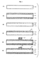
- Fig. 1 is a schematic cross-sectional view conceptually showing an example of the production processes of a photovoltaic cell of the present invention.
- numerical symbol 10 indicates a p-type semiconductor substrate
- numerical symbol 12 indicates an n-type diffusion layer
- numerical symbol 14 indicates a p + -type diffusion layer
- numerical symbol 16 indicates an anti-reflection film
- numerical symbol 18 indicates a surface electrode
- numerical symbol 20 indicates a back electrode (electrode layer), respectively.
- like numerals refer to like components, and the description thereof is omitted.
- a silicon substrate is used as a p-type semiconductor substrate will be described, but a semiconductor substrate in the invention in not limited to a silicon substrate.
- Fig. 1(1) an alkaline solution is applied onto a silicon substrate which is a p-type semiconductor substrate 10 to remove a damaged layer, and a texture structure is obtained by etching.
- the damaged layer of the silicon surface which is caused when being sliced from an ingot, is removed using 20%-by-mass caustic soda. Then, a texture structure is formed by etching with a mixture of 1% by mass of caustic soda and 10% by mass of isopropyl alcohol (in the drawing, the texture structure is omitted).
- a texture structure is formed by etching with a mixture of 1% by mass of caustic soda and 10% by mass of isopropyl alcohol (in the drawing, the texture structure is omitted).
- the composition for forming an n-type diffusion layer is applied on a front surface (that is, a surface to be a light-receiving surface) of the p-type semiconductor substrate 10, thereby forming an n-type diffusion layer-forming composition layer 11.
- the application method is not particularly restricted, and examples thereof include a printing method, a spin-coat method, brush application, a spray method, a doctor blade method, a roll coater method, and an inkjet method.
- a printing method in particular, a screen printing method is suitable.
- the amount of the composition for forming an n-type diffusion layer to be applied is not particularly restricted, and for example, may be an amount such that the amount of glass powder is from 0.01g/m 2 to 100g/m 2 , and preferably from 0.1g/m 2 to 10g/m 2 .
- a process of heat treating a substrate, on which the composition for forming an n-type diffusion layer has been applied may be needed in order to remove at least a part of the solvent contained in the composition.
- the heat treatment may be carried out under conditions such as a temperature of from 80°C to 300°C, and for about 1 minute to 10 minutes when a hot plate is used, or for about 10 minutes to 30 minutes when a dryer or the like is used.
- the heat treatment conditions depend on the solvent formulation of the composition for forming an n-type diffusion layer, but the invention is not limited thereto.
- a process of heat treating a substrate, on which the composition for forming an n-type diffusion layer has been applied may be needed in order to volatilize and remove at least a part of the dispersion medium, in particular, a binder (resin component) contained in the composition.
- the heat treatment may be carried out under conditions of a temperature of higher than 300°C and 800°C or less for 1 minute to 10 minutes.
- a known continuous furnace, batch furnace, or the like may be applied.
- both of a heat treatment at the above-mentioned temperature of from 80°C to 300°C and a heat treatment at a temperature of higher than 300°C and 800°C or less may be performed (in other words, two heat treatments are performed under different temperature conditions), or only one heat treatment under either temperature may be performed.
- the method of producing a p + -type diffusion layer (high concentration electric field layer) 14 on the back surface is not limited to a method of converting an n-type diffusion layer into a p-type diffusion layer using aluminum, and any conventionally known method may be employed, leading to increase in choices of the production methods. Accordingly, for example, a composition containing an element of Group 13 of the periodic table such as B (boron) may be applied to form a composition layer 13, thereby forming a p + -type diffusion layer 14.
- B boron
- composition containing an element of Group 13 of the periodic table such as B (boron)
- B (boron) examples include a p-type diffusion layer-forming composition which is produced in a similar manner to the composition for forming an n-type diffusion layer, except that a glass powder containing an acceptor element is used in place of the glass powder containing a donor element.
- the acceptor element may be any element as long as it is an element of Group 13 of the periodic table, and examples thereof include B (boron), A1 (aluminum) and Ga (gallium).
- the glass powder containing an acceptor element preferably includes at least one selected from the group consisting of B 2 O 3 , Al 2 O 3 , and Ga 2 O 3 .
- the method of applying the p-type diffusion layer-forming composition on the back surface of a silicon substrate is similar to the above-mentioned method of applying the composition for forming an n-type diffusion layer on a silicon substrate.
- a p + -type diffusion layer 14 may be formed on the back surface.
- the thermal diffusion treatment of the p-type diffusion layer-forming composition is preferably performed simultaneously with a thermal diffusion treatment of the composition for forming an n-type diffusion layer.
- the p-type semiconductor substrate 10, on which the n-type diffusion layer-forming composition layer 11 has been formed is subjected to a thermal diffusion treatment.
- the treatment temperature is preferably from 800°C to 1000°C, and more preferably from 850°C to 980°C.
- the treatment time is preferably from 5 minutes to 60 minutes.
- a donor element is diffused into a semiconductor substrate as illustrated in Fig. 1(3) to form an n-type diffusion layer 12.
- a known continuous furnace, batch furnace, or the like may be applied.
- the furnace atmosphere may be appropriately adjusted with air, oxygen, nitrogen, or the like.
- the phosphate glass is removed by etching.
- the etching may be carried out by a known method, including a method of dipping a subject in an acid, such as hydrofluoric acid, a method of dipping a subject in an alkali, such as caustic soda, or the like. In terms of etching capability, an etching treatment with hydrofluoric acid is preferred.
- the time of dipping is not particularly limited, and generally is from 0.5 minutes to 30 minutes, and preferably from 1 minute to 10 minutes.
- an n-type diffusion layer 12 is formed in a desired region, while no unnecessary n-type diffusion layer is formed neither on a back surface nor on a side surface.
- a side etching process for the removal of an unnecessary n-type diffusion layer formed on the side surface is essential for a method of forming an n-type diffusion layer by the conventionally widely used gas-phase reaction method, while the side etching process is unnecessary, and the process is simplified in the production method of the present invention,.
- a uniform n-type diffusion layer having a desired shape is formed in a desired region in a short time.
- the conventional production method needs the conversion of an unnecessary n-type diffusion layer formed on the back surface into a p-type diffusion layer
- the conversion method employs a method involving coating the n-type diffusion layer of the back surface with a paste of aluminum, which is an element of Group 13 of the periodic table, followed by sintering to diffuse aluminum into the n-type diffusion layer and convert the n-type diffusion layer into a p-type diffusion layer. Since an amount of aluminum higher than a certain level is required to achieve sufficient conversion into a p-type diffusion layer and to form a high concentration electric field layer of the p-type diffusion layer in this method, it is needed to form a thick aluminum layer.
- the method of producing a p + -type diffusion layer (high concentration electric field layer) 14 on the back surface may employ any method without being limited to the method involving conversion of an n-type diffusion layer into a p-type diffusion layer using aluminum, thereby increasing choices for the production method.
- the p-type diffusion layer forming composition which is configured similarly to a composition for forming an n-type diffusion layer except that a glass powder containing an acceptor element is used in place of the glass powder containing a donor element on a back surface of a silicon substrate (the opposite surface to the surface to which the n-type diffusion layer forming composition is provided), followed by a thermal diffusion treatment, whereby the p + -type diffusion layer (high concentration electric field layer) 14 is formed on the back surface.
- the material used for a back electrode 20 is not limited to aluminum of Group 13 of the periodic table.
- Ag silver
- Cu copper
- the thickness of the surface electrode 20 of the back surface may be further reduced as compared to the conventional one.
- an anti-reflection film 16 is formed over the n-type diffusion layer 12.
- the anti-reflection film 16 is formed by a known technique.
- the anti-reflection film 16 is a silicon nitride film
- the anti-reflection film 16 is formed by a plasma CVD method using a mixed gas of SiH 4 and NH 3 as a raw material.
- hydrogen diffuses into crystals, and an orbit which does not contribute to bonding of silicon atoms, that is, a dangling bond binds to hydrogen, which inactivates a defect (hydrogen passivation).
- the anti-reflection film 16 is formed under the conditions of a mixed gas flow ratio (NH 3 /SiH 4 ) of from 0.05 to 1.0, a reaction chamber pressure of from 13.3 Pa (0.1 Torr) to 266.6 Pa (2 Torr), a film-forming temperature of from 300°C to 550°C, and a plasma discharge frequency of 100 kHz or higher.
- a mixed gas flow ratio (NH 3 /SiH 4 ) of from 0.05 to 1.0
- a reaction chamber pressure of from 13.3 Pa (0.1 Torr) to 266.6 Pa (2 Torr)
- a film-forming temperature of from 300°C to 550°C
- a plasma discharge frequency 100 kHz or higher.
- a metal paste for a surface electrode is printed and applied on the anti-reflection film 16 of the front surface (light-receiving side) by a screen printing method, followed by drying, thereby forming a metal paste layer 17 for a surface electrode.
- the metal paste for a surface electrode contains (1) a metal particle and (2) a glass particle as essential components, and optionally (3) a resin binder, (4) other additives, or the like.
- a metal paste layer 19 for a back electrode is also formed on the p + -type diffusion layer 14 of the back surface.
- the constituent material and forming method of the metal paste layer 19 for a back electrode are not particularly limited in the present invention.
- the metal paste layer 19 for a back electrode may also be formed by applying a back surface electrode paste containing a metal such as aluminum, silver or copper, followed by drying.
- a portion of the back surface may also be provided with a silver paste for forming a silver electrode, for connection between photovoltaic cell elements in the module process.
- metal paste layer 17 for an electrode is sintered to complete a photovoltaic cell element.
- the front surface side undergoes melting of the anti-reflection film 16 which is an insulating film, owing to the glass particles contained in the electrode-forming metal paste, and the surface of the p-type semiconductor substrate 10 is also partially melted, by which metal particles (for example, silver particles) in the paste form a contact with the p-type semiconductor substrate 10, followed by solidification.
- metal particles for example, silver particles
- electrical conduction is made between the formed surface electrode 18 and the p-type semiconductor substrate 10. This process is called fire-through.
- the metal paste for a back electrode of the metal paste layer 19 for a back electrode is sintered to form a back electrode 20.
- Fig. 2 the shape of the surface electrode 18 is described by referring to Fig 2 .
- numerical symbol 30 indicates a bus bar electrode and numerical symbol 32 indicates a finger electrode.
- the surface electrode 18 is constituted by a bus bar electrode 30 and a finger electrode 32 intersecting the bus bar electrode 30.
- Fig. 2A is a plan view of a photovoltaic cell element, as seen from the front surface thereof, provided with the surface electrode 18 which is constituted by the bus bar electrodes 30 and the finger electrodes 32 intersecting the bus bar electrodes 30, and
- Fig. 2B is a partially enlarged perspective view of Fig. 2A .
- the surface electrode 18 may be formed, for example, by the above-mentioned screen printing of a metal paste, or plating of an electrode material, deposition of an electrode material by electron beam heating under high vacuum, or the like. It is well known that the surface electrode 18 formed from the bus bar electrode 30 and the finger electrode 32 is typically used as an electrode for the light-receiving surface side, and a known method for the formation of the bus bar electrode and the finger electrode of the light-receiving surface side may be applied.
- a photovoltaic cell having an n-type diffusion layer formed on the front surface, a p + -type diffusion layer formed on the back surface, and a front surface electrode and a back electrode disposed on the respective layers is described above, the use of the composition for forming an n-type diffusion layer enables the production of a back contact photovoltaic cell element.
- the back contact photovoltaic cell element is a photovoltaic cell element in which all electrodes are arranged on the back surface to make the area of the light receiving surface large.
- the back contact photovoltaic cell element needs to have a pn junction structure by forming both of an n-type diffusion region and a p + -type diffusion region on the back surface.
- the composition for forming an n-type diffusion layer of the invention is capable of forming an n-type diffusion region on a specific region, and thus is suitably applied to the production of a back contact photovoltaic cell element.
- the present invention also includes use of the composition for forming an n-type diffusion layer in the production of an n-type diffusion layer, and use of the composition for forming an n-type diffusion layer in the production of a photovoltaic cell element including a semiconductor substrate, n-type diffusion layer, and electrode.
- the composition for forming an n-type diffusion layer according to the invention it is possible to obtain a uniform n-type diffusion layer in a specific region in a desired shape in a short time without forming an unnecessary n-type diffusion layer.
- a photovoltaic cell element having such an n-type diffusion layer is obtained without forming an unnecessary n-type diffusion layer.
- the particle shape of the glass was observed and judged using a scanning electron microscope TYPE TM-1000 (manufactured by Hitachi High-Technologies Corporation).
- the average particle diameter of the glass was calculated using LS 13 320 LASER DIFFRACTION PARTICLE SIZE ANALYZER (measurement wavelength: 632 nm; manufactured by Beckman Coulter, Inc.).
- the viscosity of the composition for forming an n-type diffusion layer was measured using an E-type viscometer TYPE-EHD (manufactured by TOKYO KEIKI Inc.) under conditions that the amount of a sample was 0.4 ml and the number of revolutions was rpm.
- the softening temperature of the glass was determined from a differential thermal analysis (DTA) curve or the like obtained using DTG-60H SIMULTANEOUS THERMOGRAVIMETRY/DIFFERENTIAL THERMAL ANALYZER (manufactured by Shimadzu Scientific Instruments), and the temperature was estimated to be about 800°C.
- DTA differential thermal analysis
- the prepared paste was applied by screen printing, and dried at 150°C for 5 minutes on a hot plate, thereby forming a layer.
- the layer was subjected to a heat treatment in an electric furnace whose temperature was set to 500°C for 5 minutes, and then subjected to a thermal diffusion treatment in another electric furnace for diffusion whose temperature was set to 950°C for 10 minutes.
- the substrate was dipped in hydrofluoric acid for 5 minutes, followed by cleaning with flowing water and drying.
- the sheet resistance of the surface on the side on which the composition for forming an n-type diffusion layer was applied was 45 ⁇ / ⁇ .
- P phosphorus
- an n-type diffusion layer was formed on the surface of the n-type diffusion layer.
- the sheet resistance of the back surface exceeded the measurement upper limit and was thus not able to be measured, and no n-type diffusion layer was formed.
- the sheet resistance was measured by a four-probe method at 25° using a low resistivity meter LORESTA-EP MCP-T360 (manufactured by Mitsubishi Chemical Corporation).
- the prepared paste was applied by screen printing, and dried at 150°C for 5 minutes on a hot plate, thereby forming a layer.
- the layer was subjected to a heat treatment in an electric furnace whose temperature was set to 500°C for 5 minutes, and then subjected to a thermal diffusion treatment in another electric furnace for diffusion whose temperature was set to 950°C for 10 minutes.
- the substrate was dipped in hydrofluoric acid for 5 minutes, followed by cleaning with flowing water and drying.
- the sheet resistance of the surface on the side on which the composition for forming an n-type diffusion layer was applied was 38 ⁇ / ⁇ .
- P phosphorus
- an n-type diffusion layer was formed on the surface of the n-type diffusion layer.
- the sheet resistance of the back surface exceeded the measurement upper limit and was thus not able to be measured, and no n-type diffusion layer was formed.
- the prepared paste was applied by screen printing, and dried at 150°C for 5 minutes on a hot plate, thereby forming a layer.
- the layer was subjected to a heat treatment in an electric furnace whose temperature was set to 500°C for 5 minutes, and then subjected to a thermal diffusion treatment in another electric furnace for diffusion whose temperature was set to 950°C for 10 minutes.
- the substrate was dipped in hydrofluoric acid for five minutes, followed by cleaning with flowing water and drying.
- the sheet resistance of the surface on the side on which the composition for forming an n-type diffusion layer was applied was 35 ⁇ / ⁇ .
- P phosphorus
- an n-type diffusion layer was formed on the surface of the n-type diffusion layer.
- the sheet resistance of the back surface exceeded the measurement upper limit and was not able to be measured, and no n-type diffusion layer was formed.
- the prepared paste was applied by screen printing, and dried at 150°C for 5 minutes on a hot plate, thereby forming a layer.
- the layer was subjected to a heat treatment in an electric furnace whose temperature was set to 500°C for 5 minutes, and then subjected to a thermal diffusion treatment in another electric furnace for diffusion whose temperature was set to 950°C for 10 minutes.
- the substrate was dipped in hydrofluoric acid for 5 minutes, followed by cleaning with flowing water and drying.
- the sheet resistance of the surface on the side on which the composition for forming an n-type diffusion layer was applied was 51 ⁇ / ⁇ .
- P phosphorus
- the sheet resistance of the back surface was 60 ⁇ / ⁇ , and an n-type diffusion layer was formed also on the back surface.
- ammonium dihydrogen phosphate (NH 4 H 2 PO 4 ) powder 7 g of pure water, 0.7 g of polyvinyl alcohol, and 1.5 g of isopropyl alcohol were mixed using an automatic mortar kneading machine to prepare a solution, thereby preparing a composition for an n-type diffusion layer.
- the prepared solution was applied using a spin coater (2000 rpm, 30 sec), and dried at 150°C for 5 minutes on a hot plate, thereby forming a layer.
- the layer was subjected to a heat treatment in an electric furnace whose temperature was set to 500°C for 5 minutes, and then subjected to a thermal diffusion treatment in another electric furnace for diffusion whose temperature was set to 950°C for 10 minutes.
- the substrate was dipped in hydrofluoric acid for 5 minutes, followed by cleaning with flowing water and drying.
- the sheet resistance of the surface on the side on which the composition for forming an n-type diffusion layer was applied was 43 ⁇ / ⁇ .
- P phosphorus
- the sheet resistance of the back surface was 55 ⁇ / ⁇ , and an-type diffusion layer was formed also on the back surface.
Landscapes
- Engineering & Computer Science (AREA)
- Computer Hardware Design (AREA)
- Physics & Mathematics (AREA)
- Condensed Matter Physics & Semiconductors (AREA)
- General Physics & Mathematics (AREA)
- Microelectronics & Electronic Packaging (AREA)
- Power Engineering (AREA)
- Manufacturing & Machinery (AREA)
- Electromagnetism (AREA)
- Life Sciences & Earth Sciences (AREA)
- Sustainable Development (AREA)
- Sustainable Energy (AREA)
- Photovoltaic Devices (AREA)
Abstract


Description
- the present invention relates to a composition for forming an n-type diffusion layer for a photovoltaic cell element, a method of producing an n-type diffusion layer for a photovoltaic cell element, and a method of producing a photovoltaic cell element. More specifically, the present invention relates to a technique that enables the formation of an n-type diffusion layer on a specific portion of a silicon semiconductor substrate.
- The production process of a conventional silicon photovoltaic cell element will be described.
- In order to obtain a high efficiency by promoting a light confinement effect, a p-type silicon substrate is prepared wherein a texture structure is formed on a light receiving surface of the p-type silicon substrate, and subsequently, the silicon substrate is subjected to a treatment under an atmosphere of a mixed gas of phosphorus oxychloride (POCl3), which is a donor element-containing compound, nitrogen, and oxygen for several tens of minutes at from 800°C to 900°C to form an n-type diffusion layer uniformly. Since the diffusion of phosphorus is carried out using a mixed gas in the conventional method, an n-type diffusion layer is formed not only on a front surface but also on a side surface and a back surface. For this reason, a side etching process is needed for removing the n-type diffusion layer on the side surface. The n-type diffusion layer on the back surface needs to be converted to a p+-type diffusion layer, and the n-type diffusion layer has been converted to a p+-type diffusion layer by means of aluminum diffusion by providing an aluminum paste on the n-type diffusion layer of the back surface.
- On the other hand, in the field of semiconductor manufacturing, a method in which an n-type diffusion layer is formed by applying a solution containing, as a donor element-containing compound, a phosphoric acid salt such as phosphorus pentaoxide (P2O5) or ammonium dihydrogen phosphate (NH4H2PO4), is proposed (see, for example, Japanese Patent Application Laid-Open (
JP-A) No. 2002-75894 Japanese Patent No. 4073968 - However, in the methods above, a donor element or a compound containing a donor element scatters from a solution or paste, which is a diffusion source, and thus, phosphorus diffuses on a side surface and a back surface during the formation of a diffusion layer, similarly to in the above gas phase reaction method in which the mixed gas is used.
- As mentioned above, in the case of forming an n-type diffusion layer in a gas phase reaction using phosphorus oxychloride, an n-type diffusion layer is formed not only on one surface (usually a light receiving surface, or a front surface), which originally needs an n-type diffusion layer, but also on the other surface (non-light receiving surface, or a back surface) or on a side surface. Further, in a method in which a solution or paste including a compound containing phosphorus is applied and thermally diffused, an n-type diffusion layer is formed on a surface other than the front surface. For this reason, in order for a photovoltaic cell element to have a pn junction structure, etching is needed on the side surface, and the n-type diffusion layer needs to be converted into a p-type diffusion layer on the back surface. In general, a paste of aluminum, which is an element of
Group 13 of the periodic table, is applied on a back surface, and sintering is performed to convert an n-type diffusion layer to a p-type diffusion layer. Further, in a conventionally known method in which a paste containing a donor element such as phosphorus is applied as a diffusion source, it is difficult to form a diffusion layer selectively in a specific region since a donor element-containing compound becomes a vaporized gas, and the gas diffuses towards a region other than a region in which diffusion is needed. - The present invention has been made in view of the above problems of the related art, and aims to provide: a composition for forming an n-type diffusion layer, which can be applied to the production of a photovoltaic cell element using a semiconductor substrate, and which enables the formation of an n-type diffusion layer in a specific region without forming an n-type diffusion layer in a region in which the formation thereof is not needed; a method of producing an n-type diffusion layer; and a method of producing a photovoltaic cell element. Solution to Problem
- Means for solving the problems are as follows.
- <1> A composition for forming an n-type diffusion layer, the composition comprising: a glass powder comprising P2O5, SiO2 and CaO; and a dispersion medium.
- <2> The composition for forming an n-type diffusion layer according to above <1>, wherein the glass powder comprises P2O5 in an amount of from 20 mol% to 50 mol%, SiO2 in an amount of from 30 mol% to 70 mol%, and CaO in an amount of from 2 mol% to 30 mol%.
- <3> The composition for forming an n-type diffusion layer according to above <1> or <2>, wherein the glass powder has a volume average particle diameter of 10 µm or less.
- <4> The composition for forming an n-type diffusion layer according to any one of above <1> to <3>, wherein the glass powder is present in an amount of from 1% by mass to 30% by mass with respect to a total mass.
- <5> The composition for forming an n-type diffusion layer according to any one of above <1> to <4>, having a viscosity of from 1 Pa·s to 500 Pa·s.
- <6> The composition for forming an n-type diffusion layer according to any one of above <1> to <5>, wherein the dispersion medium comprises at least one selected from terpineol or butyl carbitol acetate.
- <7> The composition for forming an n-type diffusion layer according to any one of above <1> to <6>, wherein the dispersion medium comprises ethyl cellulose.
- <8> A method of producing an n-type diffusion layer, the method comprising the processes of:
- applying the composition for forming an n-type diffusion layer according to any one of above <1> to <7> onto a semiconductor substrate; and
- subjecting the semiconductor substrate, on which the composition for forming an n-type diffusion layer has been applied, to a thermal diffusion treatment to form an n-type diffusion layer.
- <9> The method of producing an n-type diffusion layer according to above <8>, wherein a temperature of the thermal diffusion treatment is from 800°C to 1000°C.
- <10> The method of producing an n-type diffusion layer according to above <8> or 9, further comprising, prior to the thermal diffusion treatment, heat treating the semiconductor substrate, on which the composition for forming an n-type diffusion layer has been applied, at a temperature of from 80°C to 300°C to remove at least a part of the dispersion medium comprised in the composition for forming an n-type diffusion layer.
- <11> The method of producing an n-type diffusion layer according to any one of above <8> to <10>, further comprising, prior to the thermal diffusion treatment, heat treating the semiconductor substrate, on which the composition for forming an n-type diffusion layer has been applied, at a temperature from higher than 300°C to 800°C to remove at least a part of the dispersion medium comprised in the composition for forming an n-type diffusion layer.
- <12> The method of producing an n-type diffusion layer according to any one of above <8> to <11>, further comprising, after the thermal diffusion treatment, etching a surface of the n-type diffusion layer formed on the semiconductor substrate using hydrofluoric acid.
- <13> A method of producing a photovoltaic cell element, the method comprising the processes of:
- applying the composition for forming an n-type diffusion layer according to any one of above <1> to <7> onto a semiconductor substrate;
- subjecting the semiconductor substrate, on which the composition for forming an n-type diffusion layer has been applied, to a thermal diffusion treatment to form an n-type diffusion layer; and
- forming an electrode on the formed n-type diffusion layer.
- <14> Use of the composition for forming an n-type diffusion layer according to any one of above <1> to <7> in the production of the n-type diffusion layer.
- <15> Use of the composition for forming an n-type diffusion layer according to any one of above <1> to <7> in the production of a photovoltaic cell element comprising a semiconductor substrate, an n-type diffusion layer, and an electrode.
- According to the invention, a composition for forming an n-type diffusion layer which is applicable to the production of a photovoltaic cell element using a semiconductor substrate, and which enables the formation of an n-type diffusion layer in a specific region without forming an n-type diffusion layer in a region in which the formation thereof is not needed; a method of producing an n-type diffusion layer; and a method of producing a photovoltaic cell element, are provided.
-
-
Fig. 1 is a schematic cross-sectional view conceptually showing an example of the method of producing a photovoltaic cell according to the present invention. -
Fig. 2A is a plan view of the photovoltaic cell element seen from a front surface. -
Fig. 2B is a partially enlarged perspective view ofFig. 2A . - First, a composition for forming an n-type diffusion layer of the invention will be described, and then, a method of producing an n-type diffusion layer using the composition for forming an n-type diffusion layer and a method of producing a photovoltaic cell element will be described.
- As used herein, the term "process" includes an independent process as well as a process which cannot be clearly separated from other processes provided the intended actions of such a process is achieved. Further, as used herein, a numerical range expressed by "A to B" refers to a range including A and B as the minimum value and the maximum value, respectively. Furthermore, when a composition has plural substances corresponding to one component, the amount of the component in the composition means the total amount of the plural substances contained in the composition, unless otherwise specified.
- A composition for forming an n-type diffusion layer of the invention contains a glass powder (hereafter, also simply referred to as "glass powder") at least including P2O5, SiO2 and CaO, and a dispersion medium, and may further contain other additives as needed in consideration of the application capacity (coating property) of the composition.
- Here, a composition for forming an n-type diffusion layer refers to a material which contains a glass powder containing a donor element, and which is capable of forming an n-type diffusion layer by application of the composition onto a semiconductor substrate, followed by thermal diffusion of the donor element. By using a composition for forming an n-type diffusion layer containing a donor element-containing glass powder, an n-type diffusion layer is formed in a desired region, while an unnecessary n-type diffusion layer is not formed on a back surface or a side surface.
- Thus, when a composition for forming an n-type diffusion layer of the invention is employed, a side etching process, which is indispensable in the widely adopted gas phase reaction method, is not needed, and the process becomes simple. Also, the process of converting an n-type diffusion layer formed on the back surface into a p+-type diffusion layer is not needed. Therefore, the method of forming a p+-type diffusion layer on the back surface, and the material, shape and thickness of the back electrode are not limited, and there is a wider choice in the production method, material and shape to be employed. As will be described in detail below, the occurrence of internal stress in the semiconductor substrate due to the thickness of the back electrode is suppressed, and warpage of a semiconductor substrate is also suppressed. Further, it is also possible to form a selective emitter structure in which the concentration of a donor element immediately under the electrode is higher than that of other portions.
- A glass powder contained in the composition for forming an n-type diffusion layer of the invention melts by sintering to form a glass layer on the n-type diffusion layer. On the other hand, a glass layer is also formed on an n-type diffusion layer in a conventional gas phase reaction method or a method in which a solution or paste containing phosphate is applied. Therefore, the glass layer formed in the present invention may be removed by etching in a similar manner to that in conventional methods. Accordingly, the composition for forming an n-type diffusion layer of the invention does not generate an unnecessary product and does not increase the number of processes, as compared with conventional methods.
- Since a donor element in a glass powder is hard to vaporize even during sintering, the formation of an n-type diffusion layer not only on a front surface but also on a back surface or a side surface due to generation of a vaporized gas is suppressed. This is thought to be because the donor element is hard to vaporize since the donor element is bonded to other elements in the glass powder or incorporated into the glass.
- As mentioned above, since it is possible to form an n-type diffusion layer having a desired concentration in a desired region by using the composition for forming an n-type diffusion layer of the invention, it is possible to form a selective region in which the concentration of the n-type donor element (dopant) is high. In contrast, it is generally difficult to form a selective region in which the concentration of the n-type donor element is high by a gas phase reaction method, which is a general method for an n-type diffusion layer, or a method in which a phosphate-containing solution is used.
- A glass powder according to the invention will be described in detail.
- A glass powder according to the invention includes a donor element. The donor element is an element which is capable of forming an n-type diffusion layer by diffusing (doping) the element in a semiconductor substrate. In the present invention, P (phosphorus) is used for a donor element. As a donor element-containing material used for introducing a donor element in a glass powder, P2O5 is used.
- The glass powder at least includes SiO2 and CaO as glass component materials.
- A glass powder according to the invention has low moisture-absorption characteristics and an excellent preservation stability since it contains a combination of P2O5 which is a donor element-containing material and SiO2 and CaO which are glass component materials. Therefore, since, even after a long-term preservation, a donor component in a glass powder is hard to vaporize during sintering, the formation of an n-type diffusion layer not only on a front surface but on a back surface or a side surface due to generation of a vaporized gas is suppressed.
- It is desirable that the content ratio of the donor element-containing material and the glass component material in the glass powder is appropriately set in consideration of the melting temperature, the softening temperature, the glass transition temperature, the chemical durability, the etching characteristics, or the like. Specifically, in terms of the water resistance, the melting temperature, and the diffusing capacity, the mole fraction of P205 contained in the glass powder is preferably from 20 mol% to 50 mol%, and more preferably from 25 mol% to 45 mol%. In terms of the water resistance, the melting temperature, and the etching characteristics, the mole fraction of SiO2 is preferably from 30 mol% to 70 mol%, and more preferably from 35 mol% to 65 mol%. In terms of the water resistance, the melting temperature, the etching characteristics, and the mole fraction of CaO is preferably from 2 mol% to 30 mol%, and more preferably from 5 mol% to 25 mol%.
- Although the total mole fraction of P2O5, SiO2, and CaO in the glass powder may be 100%, the glass powder may further include the following glass component materials other than P2O5 and SiO2, and CaO. Examples of the glass component material which can be added thereto include K2O, Na2O, Li2O, BaO, SrO, MgO, BeO, ZnO, PbO, CdO, V2O5, SnO, ZrO2, MoO3, La2O3, Nb2O5, Ta2O5, Y2O3, TiO2, ZrO2, GeO2, Al2O3, TeO2 and Lu2O3. The melting temperature, the softening temperature, the glass transition temperature, the chemical durability, or the like of the other glass component materials other than SiO2 and CaO may be controlled by adjusting the component ratios thereof as needed. When the glass powder includes a glass component material other than SiO2 and CaO, in terms of the water resistance, the melting temperature, the etching characteristics, and the diffusing capacity, the mole fraction of the glass component material other than SiO2 and CaO in the glass powder may be from 0.01 mol% to 10 mol%, and more preferably from 0.1 mol% to 5 mol%.
- In terms of the diffusing properties during a diffusion treatment and the liquid dripping, the softening temperature of the glass powder is preferably from 300°C to 1000°C, and more preferably from 400°C to 900°C. When the softening temperature is 300°C or higher, the viscosity of the glass does not become too low during the diffusion treatment, and occurrence of liquid dripping is suppressed, whereby the formation of an n-type diffusion layer on a portion other than a specific portion tends to be suppressed. When the softening temperature is 1000°C or lower, a phenomenon in which the glass powder does not melt sufficiently, and a uniform n-type diffusion layer is thus not formed, tends to be readily suppressed.
- Since, as mentioned above, the occurrence of liquid dripping is readily suppressed by setting the softening temperature of the glass powder in a range of from 300°C to 1000°C, an n-type diffusion layer tends to be readily formed on a specific region in a desired shape after a diffusion treatment. For example, when the composition for forming an n-type diffusion layer is applied in a linear pattern having a width of "a" µm, a linear pattern having a line width "b" in a range of b < 1.5a µm is retained after the diffusion treatment.
- The softening temperature of the glass powder may be determined from a differential thermal analysis (DTA) curve or the like obtained using DTG-60H Simultaneous Thermogravimetry/Differential Thermal Analyzer (available from Shimadzu Scientific Instruments).
- The shape of the glass powder may be a substantially spherical shape, a flat shape, a block shape, a plate shape, a scale-like shape, or the like. In terms of the application capacity (coating property) onto a substrate and uniform dispersion property of the composition for forming an n-type diffusion layer containing the glass powder, it is preferable that the glass powder has a substantially spherical shape, a flat shape, or a plate shape.
- The glass powder preferably has a volume average particle diameter of 10 µm or less. When a glass powder having a volume average particle diameter of 10 µm or less is used, a smooth coated film may be readily obtained. Further, the volume average particle diameter of the glass powder is more preferably 5 µm or less, further more preferably 2 µm or less, and particularly preferably 1 µm or less. The lower limit of the volume average particle diameter of the glass powder is not particularly limited, and preferably 0.01 µm or larger, and more preferably 0.05 µm or larger.
- The volume average particle diameter of the glass powder may be measured by a laser diffraction particle size analyzer or the like.
- A glass powder including P2O5, SiO2 and CaO is prepared by the following procedure.
- First, raw materials are weighed and placed in a crucible. Examples of the material for the crucible include platinum, platinum-rhodium, gold, iridium, alumina, zirconia, quartz, carbon, boron carbide, boron nitride, and silicon nitride. The material of the crucible is appropriately selected taking into consideration the melting temperature, atmosphere, reactivity with melted materials, and the like.
- Next, the raw materials are heated in an electric furnace to a temperature depending on the glass formulation, thereby preparing a melt solution. At this time, stirring is preferably applied such that the melt solution becomes homogenous.
- Subsequently, the obtained melt solution is allowed to flow on a zirconia substrate, a carbon substrate or the like to result in vitrification of the melt solution.
- Finally, the glass is pulverized into a powder. The pulverization may be carried out by a known method such as using a stamp mill, a jet mill, bead mill or ball mill.
- The content ratio of the glass powder in the composition for forming an n-type diffusion layer is determined taking into consideration the application capacity, diffusing properties of donor elements, and the like. In general, the content ratio of the glass powder in the composition for forming an n-type diffusion layer is preferably from 1% by mass to 30% by mass, more preferably from 5% by mass to 25% by mass, and further more preferably from 8% by mass to 20% by mass.
- In the invention, in terms of the water resistance, the melting temperature, the etching characteristic, and the diffusing capacity, the glass powder may include P2O5 in a mole fraction of from 20 mol% to 50 mol%, SiO2 in a mole fraction of from 30% to 70%, and CaO in a mole fraction of from 5 mol% to 25 mol%, and have a volume average particle diameter of from 0.01 µm to 2 µm; or alternatively, the glass powder may include P2O5 in a mole fraction of from 20 mol% to 50 mol%, SiO2 in a mole fraction of from 35% to 65%, and CaO in a mole fraction of from 2 mol% to 30 mol%, and have a volume average particle diameter of from 0.01 µm to 2 µm. In terms of the water resistance, the melting temperature, the etching characteristic, and the diffusing capacity, the glass powder may include P2O5 in a mole fraction of from 25 mol% to 45 mol%, SiO2 in a mole fraction of from 30% to 70%, and CaO in a mole fraction of from 2 mol% to 30 mol%, and have a volume average particle diameter of from 0.01 µm to 2 µm.
- In the invention, in terms of the water resistance, the melting temperature, the etching characteristic, and the diffusing capacity, it is more preferable that the glass powder include P2O5 in a mole fraction of from 25 mol% to 45 mol%, SiO2 in a mole fraction of from 35% to 65%, and CaO in a mole fraction of from 5 mol% to 25 mol%, and have a volume average particle diameter of from 0.01 µm to 2 µm.
- Hereinafter, a dispersion medium will be described.
- The dispersion medium is a medium which disperses the glass powder in the composition. Specifically, at least one selected from the group consisting of a binder and a solvent is employed as the dispersion medium.
- Examples of the binder which may be appropriately selected include a polyvinyl alcohol, polyacrylamide resins, polyvinyl amide resins, polyvinyl pyrrolidone, polyethylene oxide resins, polysulfonic acid, acrylamide alkylsulfonic acid, cellulose ether resins, cellulose derivatives, carboxymethylcellulose, hydroxyethylcellulose, ethyl cellulose, gelatin, starch and starch derivatives, sodium alginates and sodium alginate derivatives, xanthane and xanthane derivatives, guar gum and guar gum derivatives, scleroglucan and scleroglucan derivatives, tragacanth and tragacanth derivatives, dextrin and dextrin derivatives, (meth)acrylic acid resins, (meth)acrylic acid ester resins (for example, alkyl(meth)acrylate resins, dimethylaminoethyl (meth)acrylate resins, or the like), butadiene resins, styrene resins, and copolymers thereof. Other than these, siloxane resins or the like may be appropriately selected. These binders may be used singly or in a combination of two or more thereof. Among these, ethyl cellulose is suitable as the binder in terms of viscosity property.
- The molecular weight of the binder is not particularly restricted, and desirably is appropriately adjusted in view of a desired viscosity of the composition. For example, the content ratio of the binder in the composition may be an amount by which the following viscosity is attained.
- In view of the application property during printing, the viscosity of the composition for forming an n-type diffusion layer is preferably in a range of from 1 Pa·s to 500 Pa·s, and more preferably in a range of from 10 Pa·s to 100 Pa·s.
- The measurement of the viscosity is carried out using E-TYPE VISCOMETER TYPE-EHD (manufactured by TOKYO KEIKI, Inc.) under conditions that the amount of a sample is 0.4 ml and the number of revolutions is 5 rpm.
- Examples of the solvent include ketone solvents such as acetone, methyl ethyl ketone, methyl-n-propylketone, methyl-i-propylketone, methyl-n-butylketone, methyl-i-butylketone, methyl-n-pentylketone, methyl-n-hexylketone, diethylketone, dipropylketone, di-i-butylketone, trimethylnonanone, cyclohexanone, cyclopentanone, methylcyclohexanone, 2,4-pentanedione, or acetonylacetone; ether solvents such as diethyl ether, methyl ethyl ether, methyl-n-propyl ether, di-i-propyl ether, tetrahydrofuran, methyl tetrahydrofuran, dioxane, dimethyl dioxane, ethylene glycol dimethyl ether, ethylene glycol diethyl ether, ethylene glycol di-n-propyl ether, ethylene glycol dibutyl ether, diethylene glycol dimethyl ether, diethylene glycol diethyl ether, diethylene glycol methyl ethyl ether, diethylene glycol methyl-n-propyl ether, diethylene glycol methyl-n-butyl ether, diethylene glycol di-n-propyl ether, diethylene glycol di-n-butyl ether, diethylene glycol methyl-n-hexyl ether, triethylene glycol dimethyl ether, triethylene glycol diethyl ether, triethylene glycol methyl ethyl ether, triethylene glycol methyl-n-butyl ether, triethylene glycol di-n-butyl ether, triethylene glycol methyl-n-hexyl ether, tetraethylene glycol dimethyl ether, tetraethylene glycol diethyl ether, tetradiethylene glycol methyl ethyl ether, tetraethylene glycol methyl-n-butyl ether, diethylene glycol di-n-butyl ether, tetraethylene glycol methyl-n-hexyl ether, tetraethylene glycol di-n-butyl ether, propylene glycol dimethyl ether, propylene glycol diethyl ether, propylene glycol di-n-propyl ether, propylene glycol dibutyl ether, dipropylene glycol dimethyl ether, dipropylene glycol diethyl ether, dipropylene glycol methyl ethyl ether, dipropylene glycol methyl-n-butyl ether, dipropylene glycol di-n-propyl ether, dipropylene glycol di-n-butyl ether, dipropylene glycol methyl-n-hexyl ether, tripropylene glycol dimethyl ether, tripropylene glycol diethyl ether, tripropylene glycol methyl ethyl ether, tripropylene glycol methyl-n-butyl ether, tripropylene glycol di-n-butyl ether, tripropylene glycol methyl-n-hexyl ether, tetrapropylene glycol dimethyl ether, tetrapropylene glycol diethyl ether, tetradipropylene glycol methyl ethyl ether, tetrapropylene glycol methyl-n-butyl ether, dipropylene glycol di-n-butyl ether, tetrapropylene glycol methyl-n-hexyl ether, or tetrapropylene glycol di-n-butyl ether; ester solvents such as methyl acetate, ethyl acetate, n-propyl acetate, i-propyl acetate, n-butyl acetate, i-butyl acetate, s-butyl acetate, n-pentyl acetate, s-pentyl acetate, 3-methoxybutyl acetate, methyl pentyl acetate, 2-ethyl butyl acetate, 2-ethyl hexyl acetate, 2-(2-butoxyethoxy)ethyl acetate, benzyl acetate, cyclohexyl acetate, methyl cyclohexyl acetate, nonyl acetate, methyl acetoacetate, ethyl acetoacetate, diethylene glycol methyl ether acetate, diethylene glycol monoethyl ether acetate, diethylene glycol monobutyl ether acetate, dipropylene glycol methyl ether acetate, dipropylene glycol ethyl ether acetate, glycol diacetate, methoxy triglycol acetate, ethyl propionate, n-butyl propionate, i-amyl propionate, diethyl oxalate, di-n-butyl oxalate, methyl lactate, ethyl lactate, n-butyl lactate, n-amyl lactate, ethylene glycol methyl ether propionate, ethylene glycol ethyl ether propionate, ethylene glycol methyl ether acetate, ethylene glycol ethyl ether acetate, propylene glycol methyl ether acetate, propylene glycol ethyl ether acetate, propylene glycol propyl ether acetate, γ-butyrolactone, or γ-valerolactone; aprotic polar solvents such as acetonitrile, N-methyl pyrrolidinone, N-ethyl pyrrolidinone, N-propyl pyrrolidinone, N-butyl pyrrolidinone, N-hexyl pyrrolidinone, N-cyclohexyl pyrrolidinone, N,N-dimethyl formamide, N,N-dimethyl acetamide, or N,N-dimethyl sulfoxide; alcohol solvents such as methanol, ethanol, n-propanol, i-propanol, n-butanol, i-butanol, s-butanol, t-butanol, n-pentanol, i-pentanol, 2-methylbutanol, s-pentanol, t-pentanol, 3-methoxy butanol, n-hexanol, 2-methylpentanol, s-hexanol, 2-ethylbutanol, sec-heptanol, n-octanol, 2-ethylhexanol, s-octanol, n-nonyl alcohol, n-decanol, s-undecyl alcohol, trimethylnonyl alcohol, s-tetradecyl alcohol, s-heptadecyl alcohol, phenol, cyclohexanol, methylcyclohexanol, benzyl alcohol, ethylene glycol, 1,2-propylene glycol, 1,3-butylene glycol, diethylene glycol, dipropylene glycol, triethylene glycol, or tripropylene glycol; glycol monoether solvents such as ethylene glycol monomethyl ether, ethylene glycol monoethyl ether, ethylene glycol monophenyl ether, diethylene glycol monomethyl ether, diethylene glycol monoethyl ether, diethylene glycol mono-n-butyl ether, diethylene glycol mono-n-hexyl ether, ethoxy triglycol, tetraethylene glycol mono-n-butyl ether, propylene glycol monomethyl ether, dipropylene glycol monomethyl ether, dipropylene glycol monoethyl ether, or tripropylene glycol monomethyl ether; terpene solvents such as α-terpinene, terpinenol, myrcene, allo-ocimene, imonene, dipentene, α-pinene, β-pinene, terpinenol, carvone, ocimene or phellandrene; and water. These solvents may be used singly or in a combination of two or more thereof.
- In the composition for forming an n-type diffusion layer, in terms of the application capacity onto a substrate, the solvent is preferably at least one selected from terpineol or butyl carbitol acetate (diethylene glycol mono-n-butyl ether acetic acid). The content ratio of dispersion medium in the composition for forming an n-type diffusion layer is determined in consideration of the application capacity and the donor concentration.
- Next, a method of producing an n-type diffusion layer and method of producing a photovoltaic cell element of the invention will be described.
- The method of producing an n-type diffusion layer of the invention includes processes of: applying the above-mentioned composition for forming an n-type diffusion layer onto a semiconductor substrate; and subjecting the semiconductor substrate, on which the composition for forming an n-type diffusion layer has been applied, to a thermal diffusion treatment to form an n-type diffusion layer.
- The method of producing a photovoltaic cell element of the invention includes processes of: applying the above-mentioned composition for forming an n-type diffusion layer onto a semiconductor substrate; subjecting the semiconductor substrate, on which the composition for forming an n-type diffusion layer has been applied, to a thermal diffusion treatment to form an n-type diffusion layer; and forming an electrode on the formed n-type diffusion layer.
- Hereinafter, a description will be made with reference to
Fig. 1. Fig. 1 is a schematic cross-sectional view conceptually showing an example of the production processes of a photovoltaic cell of the present invention. InFig. 1 ,numerical symbol 10 indicates a p-type semiconductor substrate;numerical symbol 12 indicates an n-type diffusion layer;numerical symbol 14 indicates a p+-type diffusion layer;numerical symbol 16 indicates an anti-reflection film;numerical symbol 18 indicates a surface electrode; andnumerical symbol 20 indicates a back electrode (electrode layer), respectively. In the following drawings, like numerals refer to like components, and the description thereof is omitted. In the following, an example in which a silicon substrate is used as a p-type semiconductor substrate will be described, but a semiconductor substrate in the invention in not limited to a silicon substrate. - In
Fig. 1(1) , an alkaline solution is applied onto a silicon substrate which is a p-type semiconductor substrate 10 to remove a damaged layer, and a texture structure is obtained by etching. - Specifically, the damaged layer of the silicon surface, which is caused when being sliced from an ingot, is removed using 20%-by-mass caustic soda. Then, a texture structure is formed by etching with a mixture of 1% by mass of caustic soda and 10% by mass of isopropyl alcohol (in the drawing, the texture structure is omitted). Through the formation of a texture structure on the light-receiving side (front surface) of the silicon substrate, light confinement effect is promoted, and high efficiency of the photovoltaic cell element is achieved.
- In
Fig. 1(2) , the composition for forming an n-type diffusion layer is applied on a front surface (that is, a surface to be a light-receiving surface) of the p-type semiconductor substrate 10, thereby forming an n-type diffusion layer-formingcomposition layer 11. In the invention, the application method is not particularly restricted, and examples thereof include a printing method, a spin-coat method, brush application, a spray method, a doctor blade method, a roll coater method, and an inkjet method. Among these, a printing method, in particular, a screen printing method is suitable. - The amount of the composition for forming an n-type diffusion layer to be applied is not particularly restricted, and for example, may be an amount such that the amount of glass powder is from 0.01g/m2 to 100g/m2, and preferably from 0.1g/m2 to 10g/m2.
- Depending on the formulation of the composition for forming an n-type diffusion layer, prior to a thermal diffusion treatment, a process of heat treating a substrate, on which the composition for forming an n-type diffusion layer has been applied, may be needed in order to remove at least a part of the solvent contained in the composition. In this case, the heat treatment may be carried out under conditions such as a temperature of from 80°C to 300°C, and for about 1 minute to 10 minutes when a hot plate is used, or for about 10 minutes to 30 minutes when a dryer or the like is used. The heat treatment conditions depend on the solvent formulation of the composition for forming an n-type diffusion layer, but the invention is not limited thereto. By the heat treatment process, the composition for forming an n-type diffusion layer applied on the substrate is dried.
- Depending on the formulation of the composition for forming an n-type diffusion layer, prior to a thermal diffusion treatment, a process of heat treating a substrate, on which the composition for forming an n-type diffusion layer has been applied, may be needed in order to volatilize and remove at least a part of the dispersion medium, in particular, a binder (resin component) contained in the composition. In this case, the heat treatment may be carried out under conditions of a temperature of higher than 300°C and 800°C or less for 1 minute to 10 minutes. For the heat treatment, a known continuous furnace, batch furnace, or the like may be applied.
- When the heat treatment is performed, depending on the formulation of the composition for forming an n-type diffusion layer, both of a heat treatment at the above-mentioned temperature of from 80°C to 300°C and a heat treatment at a temperature of higher than 300°C and 800°C or less may be performed (in other words, two heat treatments are performed under different temperature conditions), or only one heat treatment under either temperature may be performed.
- When the production method of the invention is used, the method of producing a p+-type diffusion layer (high concentration electric field layer) 14 on the back surface is not limited to a method of converting an n-type diffusion layer into a p-type diffusion layer using aluminum, and any conventionally known method may be employed, leading to increase in choices of the production methods. Accordingly, for example, a composition containing an element of
Group 13 of the periodic table such as B (boron) may be applied to form acomposition layer 13, thereby forming a p+-type diffusion layer 14. - Examples of the composition containing an element of
Group 13 of the periodic table such as B (boron) include a p-type diffusion layer-forming composition which is produced in a similar manner to the composition for forming an n-type diffusion layer, except that a glass powder containing an acceptor element is used in place of the glass powder containing a donor element. The acceptor element may be any element as long as it is an element ofGroup 13 of the periodic table, and examples thereof include B (boron), A1 (aluminum) and Ga (gallium). The glass powder containing an acceptor element preferably includes at least one selected from the group consisting of B2O3, Al2O3, and Ga2O3. - The method of applying the p-type diffusion layer-forming composition on the back surface of a silicon substrate is similar to the above-mentioned method of applying the composition for forming an n-type diffusion layer on a silicon substrate.
- By subjecting the p-type diffusion layer-forming composition applied on the back surface to a thermal diffusion treatment similarly to the thermal diffusion treatment described below of the composition for forming an n-type diffusion layer, a p+-
type diffusion layer 14 may be formed on the back surface. The thermal diffusion treatment of the p-type diffusion layer-forming composition is preferably performed simultaneously with a thermal diffusion treatment of the composition for forming an n-type diffusion layer. - Subsequently, the p-
type semiconductor substrate 10, on which the n-type diffusion layer-formingcomposition layer 11 has been formed, is subjected to a thermal diffusion treatment. The treatment temperature is preferably from 800°C to 1000°C, and more preferably from 850°C to 980°C. The treatment time is preferably from 5 minutes to 60 minutes. By the thermal diffusion treatment, a donor element is diffused into a semiconductor substrate as illustrated inFig. 1(3) to form an n-type diffusion layer 12. For the thermal diffusion treatment, a known continuous furnace, batch furnace, or the like may be applied. When performing the thermal diffusion treatment, the furnace atmosphere may be appropriately adjusted with air, oxygen, nitrogen, or the like. - Since a glass layer (not shown) made of phosphate glass or the like is formed on the surface of the formed n-
type diffusion layer 12, the phosphate glass is removed by etching. The etching may be carried out by a known method, including a method of dipping a subject in an acid, such as hydrofluoric acid, a method of dipping a subject in an alkali, such as caustic soda, or the like. In terms of etching capability, an etching treatment with hydrofluoric acid is preferred. When a method of dipping a subject in a hydrofluoric acid is used, the time of dipping is not particularly limited, and generally is from 0.5 minutes to 30 minutes, and preferably from 1 minute to 10 minutes. - As shown in
Fig. 1(2) and 1(3) , in the n-type diffusion layer-forming method of the invention, an n-type diffusion layer 12 is formed in a desired region, while no unnecessary n-type diffusion layer is formed neither on a back surface nor on a side surface. - Accordingly, a side etching process for the removal of an unnecessary n-type diffusion layer formed on the side surface is essential for a method of forming an n-type diffusion layer by the conventionally widely used gas-phase reaction method, while the side etching process is unnecessary, and the process is simplified in the production method of the present invention,. Thus, by the production method of the invention, a uniform n-type diffusion layer having a desired shape is formed in a desired region in a short time.
- Further, the conventional production method needs the conversion of an unnecessary n-type diffusion layer formed on the back surface into a p-type diffusion layer, and the conversion method employs a method involving coating the n-type diffusion layer of the back surface with a paste of aluminum, which is an element of
Group 13 of the periodic table, followed by sintering to diffuse aluminum into the n-type diffusion layer and convert the n-type diffusion layer into a p-type diffusion layer. Since an amount of aluminum higher than a certain level is required to achieve sufficient conversion into a p-type diffusion layer and to form a high concentration electric field layer of the p-type diffusion layer in this method, it is needed to form a thick aluminum layer. However, since the coefficient of the thermal expansion of aluminum is considerably different from the coefficient of the thermal expansion of the silicon which is used as a substrate, such a difference results in generation of heavy internal stress in the silicon substrate during the sintering and cooling processes, which contributes to warpage of the silicon substrate. - Such internal stress damages the grain boundary of crystals, resulting in the problem of an increase in power loss. Warpage readily leads to damage of a photovoltaic cell element in the conveyance of the photovoltaic cell element or in the connection with a copper wiring referred to as a tab wiring (wiring member), during a module process. In recent years, advancement in slice processing techniques has led to the reduction in thickness of a silicon substrate, which results in a tendency for the photovoltaic cell element to be more readily cracked.
- In contrast, since, by the production method of the invention, no unnecessary n-type diffusion layer is formed on the back surface, there is no need for the conversion of an n-type diffusion layer into a p-type diffusion layer, which consequently abolishes the necessity of making the aluminum layer thicker. As a result, it is possible to suppress the generation of internal stress in the silicon substrate or warpage. Accordingly, it is possible to suppress an increase in power loss, or damage to a photovoltaic cell element.
- Further, in the production method of the invention, the method of producing a p+-type diffusion layer (high concentration electric field layer) 14 on the back surface may employ any method without being limited to the method involving conversion of an n-type diffusion layer into a p-type diffusion layer using aluminum, thereby increasing choices for the production method.
- For example, it is preferable to apply the p-type diffusion layer forming composition which is configured similarly to a composition for forming an n-type diffusion layer except that a glass powder containing an acceptor element is used in place of the glass powder containing a donor element on a back surface of a silicon substrate (the opposite surface to the surface to which the n-type diffusion layer forming composition is provided), followed by a thermal diffusion treatment, whereby the p+-type diffusion layer (high concentration electric field layer) 14 is formed on the back surface.
- As will be described later, the material used for a
back electrode 20 is not limited to aluminum ofGroup 13 of the periodic table. For example, Ag (silver), Cu (copper) or the like may also be used, and the thickness of thesurface electrode 20 of the back surface may be further reduced as compared to the conventional one. - In
Fig. 1(4) , ananti-reflection film 16 is formed over the n-type diffusion layer 12. Theanti-reflection film 16 is formed by a known technique. For example, when theanti-reflection film 16 is a silicon nitride film, theanti-reflection film 16 is formed by a plasma CVD method using a mixed gas of SiH4 and NH3 as a raw material. At this time, hydrogen diffuses into crystals, and an orbit which does not contribute to bonding of silicon atoms, that is, a dangling bond binds to hydrogen, which inactivates a defect (hydrogen passivation). - More specifically, the
anti-reflection film 16 is formed under the conditions of a mixed gas flow ratio (NH3/SiH4) of from 0.05 to 1.0, a reaction chamber pressure of from 13.3 Pa (0.1 Torr) to 266.6 Pa (2 Torr), a film-forming temperature of from 300°C to 550°C, and a plasma discharge frequency of 100 kHz or higher. - In
Fig. 1(5) , a metal paste for a surface electrode is printed and applied on theanti-reflection film 16 of the front surface (light-receiving side) by a screen printing method, followed by drying, thereby forming a metal paste layer 17 for a surface electrode. The metal paste for a surface electrode contains (1) a metal particle and (2) a glass particle as essential components, and optionally (3) a resin binder, (4) other additives, or the like. - Then, a
metal paste layer 19 for a back electrode is also formed on the p+-type diffusion layer 14 of the back surface. As mentioned above, the constituent material and forming method of themetal paste layer 19 for a back electrode are not particularly limited in the present invention. For example, themetal paste layer 19 for a back electrode may also be formed by applying a back surface electrode paste containing a metal such as aluminum, silver or copper, followed by drying. In this case, a portion of the back surface may also be provided with a silver paste for forming a silver electrode, for connection between photovoltaic cell elements in the module process. - In
Fig. 1(6) , metal paste layer 17 for an electrode is sintered to complete a photovoltaic cell element. When the sintering is carried out at a temperature in the range of from 600°C to 900°C for several seconds to several minutes, the front surface side undergoes melting of theanti-reflection film 16 which is an insulating film, owing to the glass particles contained in the electrode-forming metal paste, and the surface of the p-type semiconductor substrate 10 is also partially melted, by which metal particles (for example, silver particles) in the paste form a contact with the p-type semiconductor substrate 10, followed by solidification. In this manner, electrical conduction is made between the formedsurface electrode 18 and the p-type semiconductor substrate 10. This process is called fire-through. Also on the back surface side, the metal paste for a back electrode of themetal paste layer 19 for a back electrode is sintered to form aback electrode 20. - Hereinafter, the shape of the
surface electrode 18 is described by referring toFig 2 . InFig. 2 ,numerical symbol 30 indicates a bus bar electrode andnumerical symbol 32 indicates a finger electrode. Thesurface electrode 18 is constituted by abus bar electrode 30 and afinger electrode 32 intersecting thebus bar electrode 30.Fig. 2A is a plan view of a photovoltaic cell element, as seen from the front surface thereof, provided with thesurface electrode 18 which is constituted by thebus bar electrodes 30 and thefinger electrodes 32 intersecting thebus bar electrodes 30, andFig. 2B is a partially enlarged perspective view ofFig. 2A . - The
surface electrode 18 may be formed, for example, by the above-mentioned screen printing of a metal paste, or plating of an electrode material, deposition of an electrode material by electron beam heating under high vacuum, or the like. It is well known that thesurface electrode 18 formed from thebus bar electrode 30 and thefinger electrode 32 is typically used as an electrode for the light-receiving surface side, and a known method for the formation of the bus bar electrode and the finger electrode of the light-receiving surface side may be applied. - Although a photovoltaic cell having an n-type diffusion layer formed on the front surface, a p+-type diffusion layer formed on the back surface, and a front surface electrode and a back electrode disposed on the respective layers is described above, the use of the composition for forming an n-type diffusion layer enables the production of a back contact photovoltaic cell element.
- The back contact photovoltaic cell element is a photovoltaic cell element in which all electrodes are arranged on the back surface to make the area of the light receiving surface large. In other words, the back contact photovoltaic cell element needs to have a pn junction structure by forming both of an n-type diffusion region and a p+-type diffusion region on the back surface. The composition for forming an n-type diffusion layer of the invention is capable of forming an n-type diffusion region on a specific region, and thus is suitably applied to the production of a back contact photovoltaic cell element.
- The present invention also includes use of the composition for forming an n-type diffusion layer in the production of an n-type diffusion layer, and use of the composition for
forming an n-type diffusion layer in the production of a photovoltaic cell element including a semiconductor substrate, n-type diffusion layer, and electrode. As mentioned above, by using the composition for forming an n-type diffusion layer according to the invention, it is possible to obtain a uniform n-type diffusion layer in a specific region in a desired shape in a short time without forming an unnecessary n-type diffusion layer. In addition, a photovoltaic cell element having such an n-type diffusion layer is obtained without forming an unnecessary n-type diffusion layer. - Hereinbelow, examples of the invention will be described in more detail, but the invention is not limited to these Examples. Unless otherwise specified, for all chemicals, reagents are used. Further, "%" means "% by mass" unless otherwise noted.
- Ten grams of P2O5-SiO2-CaO glass (P2O5: 30 mol%, SiO2: 60 mol%, CaO: 10 mol%) powder whose particle shape was a block shape and which had a volume average particle diameter of 0.89 µm, 5 g of ethyl cellulose, and 85 g of terpineol were mixed using an automatic mortar kneading machine to obtain a paste, thereby preparing a composition for forming an n-type diffusion layer. The viscosity of the obtained composition for forming an n-type diffusion layer was 61 Pa·s.
- The particle shape of the glass was observed and judged using a scanning electron microscope TYPE TM-1000 (manufactured by Hitachi High-Technologies Corporation). The average particle diameter of the glass was calculated using
LS 13 320 LASER DIFFRACTION PARTICLE SIZE ANALYZER (measurement wavelength: 632 nm; manufactured by Beckman Coulter, Inc.). - The viscosity of the composition for forming an n-type diffusion layer was measured using an E-type viscometer TYPE-EHD (manufactured by TOKYO KEIKI Inc.) under conditions that the amount of a sample was 0.4 ml and the number of revolutions was rpm.
- The softening temperature of the glass was determined from a differential thermal analysis (DTA) curve or the like obtained using DTG-60H SIMULTANEOUS THERMOGRAVIMETRY/DIFFERENTIAL THERMAL ANALYZER (manufactured by Shimadzu Scientific Instruments), and the temperature was estimated to be about 800°C.
- Next, on a surface of a p-type silicon substrate, the prepared paste was applied by screen printing, and dried at 150°C for 5 minutes on a hot plate, thereby forming a layer. Subsequently, the layer was subjected to a heat treatment in an electric furnace whose temperature was set to 500°C for 5 minutes, and then subjected to a thermal diffusion treatment in another electric furnace for diffusion whose temperature was set to 950°C for 10 minutes. After that, in order to remove a glass layer, the substrate was dipped in hydrofluoric acid for 5 minutes, followed by cleaning with flowing water and drying.
- The sheet resistance of the surface on the side on which the composition for forming an n-type diffusion layer was applied was 45 Ω/□. On the surface of the n-type diffusion layer, P (phosphorus) was diffused and an n-type diffusion layer was formed. The sheet resistance of the back surface exceeded the measurement upper limit and was thus not able to be measured, and no n-type diffusion layer was formed.
- The sheet resistance was measured by a four-probe method at 25° using a low resistivity meter LORESTA-EP MCP-T360 (manufactured by Mitsubishi Chemical Corporation).
- Ten grams of P2O5-SiO2-CaO glass (P2O5: 30 mol%, SiO2: 50 mol%, CaO: 20 mol%) powder whose particle shape was a block shape and which had a volume average particle diameter of 0.95 µm, 5 g of ethyl cellulose, and 85 g of butyl carbitol acetate were mixed using an automatic mortar kneading machine to obtain a paste, thereby preparing a composition for forming an n-type diffusion layer. The viscosity of the obtained composition for forming an n-type diffusion layer was 67 Pa·s.
- Next, on a surface of a p-type silicon substrate, the prepared paste was applied by screen printing, and dried at 150°C for 5 minutes on a hot plate, thereby forming a layer. Subsequently, the layer was subjected to a heat treatment in an electric furnace whose temperature was set to 500°C for 5 minutes, and then subjected to a thermal diffusion treatment in another electric furnace for diffusion whose temperature was set to 950°C for 10 minutes. After that, in order to remove a glass layer, the substrate was dipped in hydrofluoric acid for 5 minutes, followed by cleaning with flowing water and drying.
- The sheet resistance of the surface on the side on which the composition for forming an n-type diffusion layer was applied was 38 Ω/□. On the surface of the n-type diffusion layer, P (phosphorus) was diffused and an n-type diffusion layer was formed. The sheet resistance of the back surface exceeded the measurement upper limit and was thus not able to be measured, and no n-type diffusion layer was formed.
- Ten grams of P2O5-SiO2-CaO glass (P2O5: 40 mol%, SiO2: 40 mol%, CaO: 20 mol%) powder whose particle shape was a substantially spherical shape and which had a volume average particle diameter of 1.02 µm, 5 g of ethyl cellulose, and 85 g of butyl carbitol acetate were mixed using an automatic mortar kneading machine to obtain a paste, thereby preparing a composition for forming an n-type diffusion layer. The viscosity of the obtained composition for forming an n-type diffusion layer was 65 Pa·s.
- Next, on a surface of a p-type silicon substrate, the prepared paste was applied by screen printing, and dried at 150°C for 5 minutes on a hot plate, thereby forming a layer. Subsequently, the layer was subjected to a heat treatment in an electric furnace whose temperature was set to 500°C for 5 minutes, and then subjected to a thermal diffusion treatment in another electric furnace for diffusion whose temperature was set to 950°C for 10 minutes. After that, in order to remove a glass layer, the substrate was dipped in hydrofluoric acid for five minutes, followed by cleaning with flowing water and drying.
- The sheet resistance of the surface on the side on which the composition for forming an n-type diffusion layer was applied was 35 Ω/□. On the surface of the n-type diffusion layer, P (phosphorus) was diffused and an n-type diffusion layer was formed. The sheet resistance of the back surface exceeded the measurement upper limit and was not able to be measured, and no n-type diffusion layer was formed.
- Ten grams of ammonium dihydrogen phosphate (NH4H2PO4) powder, 5 g of ethyl cellulose, and 85 g of terpineol were mixed using an automatic mortar kneading machine to obtain a paste, thereby preparing a composition for an n-type diffusion layer.
- Next, on a surface of a p-type silicon substrate, the prepared paste was applied by screen printing, and dried at 150°C for 5 minutes on a hot plate, thereby forming a layer. Subsequently, the layer was subjected to a heat treatment in an electric furnace whose temperature was set to 500°C for 5 minutes, and then subjected to a thermal diffusion treatment in another electric furnace for diffusion whose temperature was set to 950°C for 10 minutes. After that, in order to remove a glass layer, the substrate was dipped in hydrofluoric acid for 5 minutes, followed by cleaning with flowing water and drying.
- The sheet resistance of the surface on the side on which the composition for forming an n-type diffusion layer was applied was 51 Ω/□. On the surface of the n-type diffusion layer, P (phosphorus) was diffused and an n-type diffusion layer was formed. The sheet resistance of the back surface, however, was 60 Ω/□, and an n-type diffusion layer was formed also on the back surface.
- One gram of ammonium dihydrogen phosphate (NH4H2PO4) powder, 7 g of pure water, 0.7 g of polyvinyl alcohol, and 1.5 g of isopropyl alcohol were mixed using an automatic mortar kneading machine to prepare a solution, thereby preparing a composition for an n-type diffusion layer.
- Next, on a surface of a p-type silicon substrate, the prepared solution was applied using a spin coater (2000 rpm, 30 sec), and dried at 150°C for 5 minutes on a hot plate, thereby forming a layer. Subsequently, the layer was subjected to a heat treatment in an electric furnace whose temperature was set to 500°C for 5 minutes, and then subjected to a thermal diffusion treatment in another electric furnace for diffusion whose temperature was set to 950°C for 10 minutes. After that, in order to remove a glass layer, the substrate was dipped in hydrofluoric acid for 5 minutes, followed by cleaning with flowing water and drying.
- The sheet resistance of the surface on the side on which the composition for forming an n-type diffusion layer was applied was 43 Ω/□. On the surface of the n-type diffusion layer, P (phosphorus) was diffused and an n-type diffusion layer was formed. The sheet resistance of the back surface, however, was 55 Ω/□, and an-type diffusion layer was formed also on the back surface.
- The disclosure of
Japanese Patent Application No. 2011-158489 filed on July 19, 2011 - All literatures, patent applications, and technical standards described herein are herein incorporated by reference to the same extent as if each individual literature, patent application, or technical standard was specifically and individually indicated as being incorporated by reference.
Claims (15)
- A composition for forming an n-type diffusion layer, the composition comprising:a glass powder comprising P2O5, SiO2 and CaO; anda dispersion medium.
- The composition for forming an n-type diffusion layer according to claim 1, wherein the glass powder comprises P2O5 in an amount of from 20 mol% to 50 mol%, SiO2 in an amount of from 30 mol% to 70 mol%, and CaO in an amount of from 2 mol% to 30 mol%.
- The composition for forming an n-type diffusion layer according to claim 1 or 2, wherein the glass powder has a volume average particle diameter of 10 µm or less.
- The composition for forming an n-type diffusion layer according to any one of claims 1 to 3, wherein the glass powder is present in an amount of from 1% by mass to 30% by mass with respect to a total mass.
- The composition for forming an n-type diffusion layer according to any one of claims 1 to 4, having a viscosity of from 1 Pa·s to 500 Pa·s.
- The composition for forming an n-type diffusion layer according to any one of claims 1 to 5, wherein the dispersion medium comprises at least one selected from terpineol or butyl carbitol acetate.
- The composition for forming an n-type diffusion layer according to any one of claims 1 to 6, wherein the dispersion medium comprises ethyl cellulose.
- A method of producing an n-type diffusion layer, the method comprising the processes of:applying the composition for forming an n-type diffusion layer according to any one of claims 1 to 7 onto a semiconductor substrate; andsubjecting the semiconductor substrate, on which the composition for forming an n-type diffusion layer has been applied, to a thermal diffusion treatment to form an n-type diffusion layer.
- The method of producing an n-type diffusion layer according to claim 8, wherein a temperature of the thermal diffusion treatment is from 800°C to 1000°C.
- The method of producing an n-type diffusion layer according to claim 8 or 9, further comprising, prior to the thermal diffusion treatment, heat treating the semiconductor substrate, on which the composition for forming an n-type diffusion layer has been applied, at a temperature of from 80°C to 300°C to remove at least a part of the dispersion medium comprised in the composition for forming an n-type diffusion layer.
- The method of producing an n-type diffusion layer according to any one of claims 8 to 10, further comprising, prior to the thermal diffusion treatment, heat treating the semiconductor substrate, on which the composition for forming an n-type diffusion layer has been applied, at a temperature from higher than 300°C to 800°C to remove at least a part of the dispersion medium comprised in the composition for forming an n-type diffusion layer.
- The method of producing an n-type diffusion layer according to any one of claims 8 to 11, further comprising, after the thermal diffusion treatment, etching a surface of the n-type diffusion layer formed on the semiconductor substrate using hydrofluoric acid.
- A method of producing a photovoltaic cell element, the method comprising the processes of:applying the composition for forming an n-type diffusion layer according to any one of claims 1 to 7 onto a semiconductor substrate;subjecting the semiconductor substrate, on which the composition for forming an n-type diffusion layer has been applied, to a thermal diffusion treatment to form an n-type diffusion layer; andforming an electrode on the formed n-type diffusion layer.
- Use of the composition for forming an n-type diffusion layer according to any one of claims 1 to 7 in the production of the n-type diffusion layer.
- Use of the composition for forming an n-type diffusion layer according to any one of claims 1 to 7 in the production of a photovoltaic cell element comprising a semiconductor substrate, an n-type diffusion layer, and an electrode.
Applications Claiming Priority (2)
| Application Number | Priority Date | Filing Date | Title |
|---|---|---|---|
| JP2011158489 | 2011-07-19 | ||
| EP12814632.1A EP2743967A4 (en) | 2011-07-19 | 2012-07-17 | Composition that forms n-type diffusion layer, n-type diffusion layer manufacturing method and solar cell element manufacturing method |
Related Parent Applications (1)
| Application Number | Title | Priority Date | Filing Date |
|---|---|---|---|
| EP12814632.1A Division EP2743967A4 (en) | 2011-07-19 | 2012-07-17 | Composition that forms n-type diffusion layer, n-type diffusion layer manufacturing method and solar cell element manufacturing method |
Publications (2)
| Publication Number | Publication Date |
|---|---|
| EP3007210A2 true EP3007210A2 (en) | 2016-04-13 |
| EP3007210A3 EP3007210A3 (en) | 2016-04-20 |
Family
ID=47558163
Family Applications (2)
| Application Number | Title | Priority Date | Filing Date |
|---|---|---|---|
| EP12814632.1A Withdrawn EP2743967A4 (en) | 2011-07-19 | 2012-07-17 | Composition that forms n-type diffusion layer, n-type diffusion layer manufacturing method and solar cell element manufacturing method |
| EP15196741.1A Withdrawn EP3007210A3 (en) | 2011-07-19 | 2012-07-17 | Composition for forming n-type diffusion layer, method of producing n-type diffusion layer, and method of producing photovoltaic cell element |
Family Applications Before (1)
| Application Number | Title | Priority Date | Filing Date |
|---|---|---|---|
| EP12814632.1A Withdrawn EP2743967A4 (en) | 2011-07-19 | 2012-07-17 | Composition that forms n-type diffusion layer, n-type diffusion layer manufacturing method and solar cell element manufacturing method |
Country Status (7)
| Country | Link |
|---|---|
| US (1) | US20150099352A1 (en) |
| EP (2) | EP2743967A4 (en) |
| JP (1) | JP5176159B1 (en) |
| KR (2) | KR101541660B1 (en) |
| CN (3) | CN103688341B (en) |
| TW (2) | TWI462157B (en) |
| WO (1) | WO2013011986A1 (en) |
Families Citing this family (5)
| Publication number | Priority date | Publication date | Assignee | Title |
|---|---|---|---|---|
| CN103688341B (en) * | 2011-07-19 | 2016-09-28 | 日立化成株式会社 | N-type diffusion layer is formed by compositions, the manufacture method of n-type diffusion layer and the manufacture method of solar cell device |
| JP2014179360A (en) * | 2013-03-13 | 2014-09-25 | Hitachi Chemical Co Ltd | Composition for n-type diffusion layer formation, method for manufacturing semiconductor substrate having n-type diffusion layer, and method for manufacturing solar battery device |
| DE102013113123B4 (en) * | 2013-11-27 | 2021-11-18 | Hanwha Q Cells Gmbh | Solar cell manufacturing process |
| DE102013113108B4 (en) * | 2013-11-27 | 2024-08-29 | Hanwha Q Cells Gmbh | Solar cell manufacturing process |
| JP6582747B2 (en) * | 2015-08-28 | 2019-10-02 | 日立化成株式会社 | Composition for forming n-type diffusion layer, method for producing semiconductor substrate having n-type diffusion layer, and method for producing solar cell |
Citations (2)
| Publication number | Priority date | Publication date | Assignee | Title |
|---|---|---|---|---|
| JP2002075894A (en) | 2000-09-01 | 2002-03-15 | Sanken Electric Co Ltd | Liquid impurity source material, and semiconductor device |
| JP4073968B2 (en) | 1997-05-30 | 2008-04-09 | アンテルユニヴェルシテール・ミクロ−エレクトロニカ・サントリュム・ヴェー・ゼッド・ドゥブルヴェ | Solar cell and manufacturing method thereof |
Family Cites Families (52)
| Publication number | Priority date | Publication date | Assignee | Title |
|---|---|---|---|---|
| NL99619C (en) * | 1955-06-28 | |||
| US6225392B1 (en) * | 1996-05-15 | 2001-05-01 | Asahi Glass Company Ltd. | Conductive paste |
| US6849334B2 (en) * | 2001-08-17 | 2005-02-01 | Neophotonics Corporation | Optical materials and optical devices |
| US6171987B1 (en) * | 1997-12-29 | 2001-01-09 | Ben-Gurion University Of The Negev | Cadmium-free and lead-free glass compositions, thick film formulations containing them and uses thereof |
| DE19910816A1 (en) * | 1999-03-11 | 2000-10-05 | Merck Patent Gmbh | Doping pastes for producing p, p + and n, n + regions in semiconductors |
| US6611372B1 (en) * | 2000-06-09 | 2003-08-26 | The Arizona Board Of Regents On Behalf Of The University Of Arizona | Erbium and ytterbium co-doped phosphate glass optical fiber amplifiers using short active fiber length |
| DE10141117A1 (en) * | 2001-08-22 | 2003-03-13 | Schott Glas | Antimicrobial silicate glass and its use |
| EP1361199B1 (en) * | 2002-04-24 | 2008-01-09 | Central Glass Company, Limited | Lead-free low-melting glass |
| US7176152B2 (en) * | 2004-06-09 | 2007-02-13 | Ferro Corporation | Lead-free and cadmium-free conductive copper thick film pastes |
| US7339780B2 (en) * | 2004-06-09 | 2008-03-04 | Ferro Corporation | Copper termination inks containing lead free and cadmium free glasses for capacitors |
| US20060102228A1 (en) * | 2004-11-12 | 2006-05-18 | Ferro Corporation | Method of making solar cell contacts |
| WO2006080557A1 (en) * | 2005-01-31 | 2006-08-03 | Kabushiki Kaisha Ohara | Glass-ceramics and method for manufacturing the same |
| JP2006294579A (en) * | 2005-03-17 | 2006-10-26 | Fujitsu Ltd | Manufacturing method of protruding body |
| US7326367B2 (en) * | 2005-04-25 | 2008-02-05 | E.I. Du Pont De Nemours And Company | Thick film conductor paste compositions for LTCC tape in microwave applications |
| JP4481869B2 (en) * | 2005-04-26 | 2010-06-16 | 信越半導体株式会社 | SOLAR CELL MANUFACTURING METHOD, SOLAR CELL, AND SEMICONDUCTOR DEVICE MANUFACTURING METHOD |
| US7771623B2 (en) * | 2005-06-07 | 2010-08-10 | E.I. du Pont de Nemours and Company Dupont (UK) Limited | Aluminum thick film composition(s), electrode(s), semiconductor device(s) and methods of making thereof |
| US7718092B2 (en) * | 2005-10-11 | 2010-05-18 | E.I. Du Pont De Nemours And Company | Aluminum thick film composition(s), electrode(s), semiconductor device(s) and methods of making thereof |
| FR2906405B1 (en) * | 2006-09-22 | 2008-12-19 | Commissariat Energie Atomique | METHOD OF MAKING DOPED REGIONS IN A SUBSTRATE AND PHOTOVOLTAIC CELL |
| JP5166745B2 (en) * | 2007-03-07 | 2013-03-21 | 信越化学工業株式会社 | Method for producing single crystal silicon solar cell |
| CN102270669A (en) * | 2007-05-09 | 2011-12-07 | 日立化成工业株式会社 | Conductor connection member, connection structure, and solar cell module |
| KR101248636B1 (en) * | 2007-05-09 | 2013-04-01 | 히타치가세이가부시끼가이샤 | Method for connecting conductor, member for connecting conductor, connecting structure and solar cell module |
| US8309844B2 (en) * | 2007-08-29 | 2012-11-13 | Ferro Corporation | Thick film pastes for fire through applications in solar cells |
| US8236598B2 (en) * | 2007-08-31 | 2012-08-07 | Ferro Corporation | Layered contact structure for solar cells |
| JP5236914B2 (en) * | 2007-09-19 | 2013-07-17 | シャープ株式会社 | Manufacturing method of solar cell |
| US20090092745A1 (en) * | 2007-10-05 | 2009-04-09 | Luca Pavani | Dopant material for manufacturing solar cells |
| NL2000999C2 (en) * | 2007-11-13 | 2009-05-14 | Stichting Energie | Process for the production of crystalline silicon solar cells using co-diffusion of boron and phosphorus. |
| KR20090080756A (en) * | 2008-01-22 | 2009-07-27 | 삼성에스디아이 주식회사 | A photosensitive paste composition, a barrier rib prepared using the composition and a plasma display panel comprising the barrier rib |
| JP5522900B2 (en) * | 2008-02-22 | 2014-06-18 | 東京応化工業株式会社 | Electrode forming conductive composition and method for forming solar cell |
| KR101631711B1 (en) * | 2008-03-21 | 2016-06-17 | 신에쓰 가가꾸 고교 가부시끼가이샤 | Phosphorus paste for diffusion and method for preparing solar cell by using the same |
| US8158504B2 (en) * | 2008-05-30 | 2012-04-17 | E. I. Du Pont De Nemours And Company | Conductive compositions and processes for use in the manufacture of semiconductor devices—organic medium components |
| TW201007773A (en) * | 2008-06-06 | 2010-02-16 | Du Pont | Glass compositions used in conductors for photovoltaic cells |
| KR101225909B1 (en) * | 2008-08-07 | 2013-01-24 | 교토 에렉스 가부시키가이샤 | Conductive paste for formation of a solar cell element electrode, solar cell element, and manufacturing method for said solar cell element |
| US8053867B2 (en) * | 2008-08-20 | 2011-11-08 | Honeywell International Inc. | Phosphorous-comprising dopants and methods for forming phosphorous-doped regions in semiconductor substrates using phosphorous-comprising dopants |
| CN102369168A (en) * | 2009-04-09 | 2012-03-07 | E.I.内穆尔杜邦公司 | Glass compositions used in conductors for photovoltaic cells |
| JP5649290B2 (en) * | 2009-07-30 | 2015-01-07 | 株式会社ノリタケカンパニーリミテド | Lead-free conductive composition for solar cell electrode |
| JP5815215B2 (en) * | 2009-08-27 | 2015-11-17 | 東京応化工業株式会社 | Diffusion agent composition and method for forming impurity diffusion layer |
| US20110315210A1 (en) * | 2009-12-18 | 2011-12-29 | E. I. Du Pont De Nemours And Company | Glass compositions used in conductors for photovoltaic cells |
| JP4868079B1 (en) * | 2010-01-25 | 2012-02-01 | 日立化成工業株式会社 | N-type diffusion layer forming composition, n-type diffusion layer manufacturing method, and solar cell manufacturing method |
| US20110195541A1 (en) * | 2010-02-05 | 2011-08-11 | Hitachi Chemical Company, Ltd. | Composition for forming n-type diffusion layer, method for forming n-type diffusion layer, and method for producing photovoltaic cell |
| EP2566823B1 (en) * | 2010-05-04 | 2016-10-05 | E. I. du Pont de Nemours and Company | Thick-film pastes containing lead-tellurium-boron-oxides, and their use in the manufacture of semiconductor devices |
| JP4978759B1 (en) * | 2010-11-17 | 2012-07-18 | 日立化成工業株式会社 | Manufacturing method of solar cell |
| US8404599B2 (en) * | 2010-11-17 | 2013-03-26 | Hitachi Chemical Company, Ltd. | Method for producing photovoltaic cell |
| KR20140009984A (en) * | 2010-11-17 | 2014-01-23 | 히타치가세이가부시끼가이샤 | Method for producing solar cell |
| US20120122265A1 (en) * | 2010-11-17 | 2012-05-17 | Hitachi Chemical Company, Ltd. | Method for producing photovoltaic cell |
| US20120325307A1 (en) * | 2010-12-16 | 2012-12-27 | E. I. Du Pont De Nemours And Company | Low bow aluminum paste with an alkaline earth metal salt additive for solar cells |
| WO2012127468A2 (en) * | 2011-03-24 | 2012-09-27 | Ben-Gurion University Of The Negev Research And Development Authority | Coatings for solar applications |
| CN103688341B (en) * | 2011-07-19 | 2016-09-28 | 日立化成株式会社 | N-type diffusion layer is formed by compositions, the manufacture method of n-type diffusion layer and the manufacture method of solar cell device |
| US20130025670A1 (en) * | 2011-07-25 | 2013-01-31 | Hitachi Chemical Company, Ltd. | Semiconductor substrate and method for producing the same, photovoltaic cell element, and photovoltaic cell |
| KR20140090607A (en) * | 2011-09-29 | 2014-07-17 | 가부시키가이샤 노리타케 캄파니 리미티드 | Lead-free conductive paste composition for solar cells |
| WO2013125253A1 (en) * | 2012-02-23 | 2013-08-29 | 日立化成株式会社 | Composition for forming n-type diffusion layer, method for producing semiconductor substrate having n-type diffusion layer, and method for producing solar cell element |
| JP2015528178A (en) * | 2012-06-12 | 2015-09-24 | ヘレウス プレシャス メタルズ ノース アメリカ コンショホーケン エルエルシー | Conductive paste with adhesion promoter |
| KR101999795B1 (en) * | 2012-06-27 | 2019-07-12 | 삼성전자주식회사 | Conductive paste and electronic device and solar cell including an electrode formed using the conductive paste |
-
2012
- 2012-07-17 CN CN201280035500.8A patent/CN103688341B/en not_active Expired - Fee Related
- 2012-07-17 JP JP2012547355A patent/JP5176159B1/en active Active
- 2012-07-17 US US14/233,704 patent/US20150099352A1/en not_active Abandoned
- 2012-07-17 WO PCT/JP2012/068122 patent/WO2013011986A1/en active Application Filing
- 2012-07-17 EP EP12814632.1A patent/EP2743967A4/en not_active Withdrawn
- 2012-07-17 KR KR1020147003094A patent/KR101541660B1/en active IP Right Grant
- 2012-07-17 CN CN201410050927.6A patent/CN103794478B/en active Active
- 2012-07-17 EP EP15196741.1A patent/EP3007210A3/en not_active Withdrawn
- 2012-07-17 KR KR1020147004451A patent/KR20140041865A/en not_active Application Discontinuation
- 2012-07-17 CN CN201510849338.9A patent/CN105489662A/en active Pending
- 2012-07-18 TW TW101125858A patent/TWI462157B/en active
- 2012-07-18 TW TW103116984A patent/TWI575762B/en not_active IP Right Cessation
Patent Citations (2)
| Publication number | Priority date | Publication date | Assignee | Title |
|---|---|---|---|---|
| JP4073968B2 (en) | 1997-05-30 | 2008-04-09 | アンテルユニヴェルシテール・ミクロ−エレクトロニカ・サントリュム・ヴェー・ゼッド・ドゥブルヴェ | Solar cell and manufacturing method thereof |
| JP2002075894A (en) | 2000-09-01 | 2002-03-15 | Sanken Electric Co Ltd | Liquid impurity source material, and semiconductor device |
Also Published As
| Publication number | Publication date |
|---|---|
| CN103794478A (en) | 2014-05-14 |
| KR20140032492A (en) | 2014-03-14 |
| KR101541660B1 (en) | 2015-08-03 |
| CN103794478B (en) | 2016-01-20 |
| CN103688341B (en) | 2016-09-28 |
| EP3007210A3 (en) | 2016-04-20 |
| JP5176159B1 (en) | 2013-04-03 |
| US20150099352A1 (en) | 2015-04-09 |
| TW201306095A (en) | 2013-02-01 |
| TW201432919A (en) | 2014-08-16 |
| WO2013011986A1 (en) | 2013-01-24 |
| EP2743967A1 (en) | 2014-06-18 |
| TWI462157B (en) | 2014-11-21 |
| CN103688341A (en) | 2014-03-26 |
| CN105489662A (en) | 2016-04-13 |
| TWI575762B (en) | 2017-03-21 |
| JPWO2013011986A1 (en) | 2015-02-23 |
| EP2743967A4 (en) | 2015-06-03 |
| KR20140041865A (en) | 2014-04-04 |
Similar Documents
| Publication | Publication Date | Title |
|---|---|---|
| EP2348546A2 (en) | Composition for forming n-type diffusion layer, method for forming n-type diffusion layer, and method for producing photovoltaic cell | |
| US9608143B2 (en) | Composition for forming N-type diffusion layer, method of forming N-type diffusion layer, and method of producing photovoltaic cell | |
| US20120184062A1 (en) | Composition for forming n-type diffusion layer, method for forming n-type diffusion layer, and method for producing photovoltaic cell | |
| EP2355137B1 (en) | Use of a composition for forming p-type diffusion layer and method for forming p-type diffusion layer | |
| JP5958485B2 (en) | N-type diffusion layer forming composition, n-type diffusion layer manufacturing method, and solar cell element manufacturing method | |
| EP3007210A2 (en) | Composition for forming n-type diffusion layer, method of producing n-type diffusion layer, and method of producing photovoltaic cell element | |
| US9520529B2 (en) | Composition for forming P-type diffusion layer, method of forming P-type diffusion layer, and method of producing photovoltaic cell | |
| KR101384874B1 (en) | COMPOSITION FOR FORMING n-TYPE DIFFUSION LAYER, METHOD FOR PRODUCING n-TYPE DIFFUSION LAYER, AND METHOD FOR PRODUCING SOLAR CELL ELEMENT | |
| US10312402B2 (en) | P-type diffusion layer forming composition | |
| KR20130066613A (en) | N-type diffusion layer forming composition, method of producing n-type diffusion layer, and method of producing solar cell element | |
| KR20140041423A (en) | Composition for forming n-type diffusion layer, process for producing n-type diffusion layer, and process for producing solar cell | |
| JP2017139420A (en) | P-type diffusion layer forming composition, method for manufacturing semiconductor substrate with p-type diffusion layer, manufacturing method for solar cell element, and solar cell element |
Legal Events
| Date | Code | Title | Description |
|---|---|---|---|
| PUAL | Search report despatched |
Free format text: ORIGINAL CODE: 0009013 |
|
| PUAI | Public reference made under article 153(3) epc to a published international application that has entered the european phase |
Free format text: ORIGINAL CODE: 0009012 |
|
| AC | Divisional application: reference to earlier application |
Ref document number: 2743967 Country of ref document: EP Kind code of ref document: P |
|
| AK | Designated contracting states |
Kind code of ref document: A2 Designated state(s): AL AT BE BG CH CY CZ DE DK EE ES FI FR GB GR HR HU IE IS IT LI LT LU LV MC MK MT NL NO PL PT RO RS SE SI SK SM TR |
|
| AK | Designated contracting states |
Kind code of ref document: A3 Designated state(s): AL AT BE BG CH CY CZ DE DK EE ES FI FR GB GR HR HU IE IS IT LI LT LU LV MC MK MT NL NO PL PT RO RS SE SI SK SM TR |
|
| RIC1 | Information provided on ipc code assigned before grant |
Ipc: H01L 31/18 20060101ALI20160317BHEP Ipc: H01L 21/225 20060101AFI20160317BHEP |
|
| STAA | Information on the status of an ep patent application or granted ep patent |
Free format text: STATUS: THE APPLICATION IS DEEMED TO BE WITHDRAWN |
|
| 18D | Application deemed to be withdrawn |
Effective date: 20161021 |