EP3002781A1 - Manufacturing method for reverse conducting insulated gate bipolar transistor - Google Patents
Manufacturing method for reverse conducting insulated gate bipolar transistor Download PDFInfo
- Publication number
- EP3002781A1 EP3002781A1 EP14838639.4A EP14838639A EP3002781A1 EP 3002781 A1 EP3002781 A1 EP 3002781A1 EP 14838639 A EP14838639 A EP 14838639A EP 3002781 A1 EP3002781 A1 EP 3002781A1
- Authority
- EP
- European Patent Office
- Prior art keywords
- type substrate
- back side
- reverse conducting
- manufacturing
- bipolar transistor
- Prior art date
- Legal status (The legal status is an assumption and is not a legal conclusion. Google has not performed a legal analysis and makes no representation as to the accuracy of the status listed.)
- Granted
Links
Images


Classifications
-
- H—ELECTRICITY
- H10—SEMICONDUCTOR DEVICES; ELECTRIC SOLID-STATE DEVICES NOT OTHERWISE PROVIDED FOR
- H10D—INORGANIC ELECTRIC SEMICONDUCTOR DEVICES
- H10D84/00—Integrated devices formed in or on semiconductor substrates that comprise only semiconducting layers, e.g. on Si wafers or on GaAs-on-Si wafers
- H10D84/60—Integrated devices formed in or on semiconductor substrates that comprise only semiconducting layers, e.g. on Si wafers or on GaAs-on-Si wafers characterised by the integration of at least one component covered by groups H10D10/00 or H10D18/00, e.g. integration of BJTs
- H10D84/611—Combinations of BJTs and one or more of diodes, resistors or capacitors
- H10D84/613—Combinations of vertical BJTs and one or more of diodes, resistors or capacitors
- H10D84/617—Combinations of vertical BJTs and only diodes
-
- H—ELECTRICITY
- H10—SEMICONDUCTOR DEVICES; ELECTRIC SOLID-STATE DEVICES NOT OTHERWISE PROVIDED FOR
- H10D—INORGANIC ELECTRIC SEMICONDUCTOR DEVICES
- H10D12/00—Bipolar devices controlled by the field effect, e.g. insulated-gate bipolar transistors [IGBT]
- H10D12/01—Manufacture or treatment
- H10D12/031—Manufacture or treatment of IGBTs
- H10D12/032—Manufacture or treatment of IGBTs of vertical IGBTs
-
- H—ELECTRICITY
- H10—SEMICONDUCTOR DEVICES; ELECTRIC SOLID-STATE DEVICES NOT OTHERWISE PROVIDED FOR
- H10D—INORGANIC ELECTRIC SEMICONDUCTOR DEVICES
- H10D12/00—Bipolar devices controlled by the field effect, e.g. insulated-gate bipolar transistors [IGBT]
- H10D12/411—Insulated-gate bipolar transistors [IGBT]
- H10D12/441—Vertical IGBTs
-
- H—ELECTRICITY
- H10—SEMICONDUCTOR DEVICES; ELECTRIC SOLID-STATE DEVICES NOT OTHERWISE PROVIDED FOR
- H10D—INORGANIC ELECTRIC SEMICONDUCTOR DEVICES
- H10D62/00—Semiconductor bodies, or regions thereof, of devices having potential barriers
- H10D62/10—Shapes, relative sizes or dispositions of the regions of the semiconductor bodies; Shapes of the semiconductor bodies
- H10D62/102—Constructional design considerations for preventing surface leakage or controlling electric field concentration
- H10D62/112—Constructional design considerations for preventing surface leakage or controlling electric field concentration for preventing surface leakage due to surface inversion layers, e.g. by using channel stoppers
-
- H—ELECTRICITY
- H10—SEMICONDUCTOR DEVICES; ELECTRIC SOLID-STATE DEVICES NOT OTHERWISE PROVIDED FOR
- H10D—INORGANIC ELECTRIC SEMICONDUCTOR DEVICES
- H10D62/00—Semiconductor bodies, or regions thereof, of devices having potential barriers
- H10D62/10—Shapes, relative sizes or dispositions of the regions of the semiconductor bodies; Shapes of the semiconductor bodies
- H10D62/13—Semiconductor regions connected to electrodes carrying current to be rectified, amplified or switched, e.g. source or drain regions
- H10D62/141—Anode or cathode regions of thyristors; Collector or emitter regions of gated bipolar-mode devices, e.g. of IGBTs
- H10D62/142—Anode regions of thyristors or collector regions of gated bipolar-mode devices
-
- H—ELECTRICITY
- H10—SEMICONDUCTOR DEVICES; ELECTRIC SOLID-STATE DEVICES NOT OTHERWISE PROVIDED FOR
- H10D—INORGANIC ELECTRIC SEMICONDUCTOR DEVICES
- H10D62/00—Semiconductor bodies, or regions thereof, of devices having potential barriers
- H10D62/10—Shapes, relative sizes or dispositions of the regions of the semiconductor bodies; Shapes of the semiconductor bodies
- H10D62/17—Semiconductor regions connected to electrodes not carrying current to be rectified, amplified or switched, e.g. channel regions
- H10D62/393—Body regions of DMOS transistors or IGBTs
-
- H—ELECTRICITY
- H10—SEMICONDUCTOR DEVICES; ELECTRIC SOLID-STATE DEVICES NOT OTHERWISE PROVIDED FOR
- H10P—GENERIC PROCESSES OR APPARATUS FOR THE MANUFACTURE OR TREATMENT OF DEVICES COVERED BY CLASS H10
- H10P30/00—Ion implantation into wafers, substrates or parts of devices
- H10P30/20—Ion implantation into wafers, substrates or parts of devices into semiconductor materials, e.g. for doping
- H10P30/202—Ion implantation into wafers, substrates or parts of devices into semiconductor materials, e.g. for doping characterised by the semiconductor materials
- H10P30/204—Ion implantation into wafers, substrates or parts of devices into semiconductor materials, e.g. for doping characterised by the semiconductor materials into Group IV semiconductors
-
- H—ELECTRICITY
- H10—SEMICONDUCTOR DEVICES; ELECTRIC SOLID-STATE DEVICES NOT OTHERWISE PROVIDED FOR
- H10P—GENERIC PROCESSES OR APPARATUS FOR THE MANUFACTURE OR TREATMENT OF DEVICES COVERED BY CLASS H10
- H10P30/00—Ion implantation into wafers, substrates or parts of devices
- H10P30/20—Ion implantation into wafers, substrates or parts of devices into semiconductor materials, e.g. for doping
- H10P30/21—Ion implantation into wafers, substrates or parts of devices into semiconductor materials, e.g. for doping of electrically active species
-
- H—ELECTRICITY
- H10—SEMICONDUCTOR DEVICES; ELECTRIC SOLID-STATE DEVICES NOT OTHERWISE PROVIDED FOR
- H10P—GENERIC PROCESSES OR APPARATUS FOR THE MANUFACTURE OR TREATMENT OF DEVICES COVERED BY CLASS H10
- H10P50/00—Etching of wafers, substrates or parts of devices
- H10P50/20—Dry etching; Plasma etching; Reactive-ion etching
- H10P50/24—Dry etching; Plasma etching; Reactive-ion etching of semiconductor materials
- H10P50/242—Dry etching; Plasma etching; Reactive-ion etching of semiconductor materials of Group IV materials
-
- H—ELECTRICITY
- H10—SEMICONDUCTOR DEVICES; ELECTRIC SOLID-STATE DEVICES NOT OTHERWISE PROVIDED FOR
- H10P—GENERIC PROCESSES OR APPARATUS FOR THE MANUFACTURE OR TREATMENT OF DEVICES COVERED BY CLASS H10
- H10P52/00—Grinding, lapping or polishing of wafers, substrates or parts of devices
-
- H—ELECTRICITY
- H10—SEMICONDUCTOR DEVICES; ELECTRIC SOLID-STATE DEVICES NOT OTHERWISE PROVIDED FOR
- H10P—GENERIC PROCESSES OR APPARATUS FOR THE MANUFACTURE OR TREATMENT OF DEVICES COVERED BY CLASS H10
- H10P34/00—Irradiation with electromagnetic or particle radiation of wafers, substrates or parts of devices
- H10P34/40—Irradiation with electromagnetic or particle radiation of wafers, substrates or parts of devices with high-energy radiation
Definitions
- the present invention relates to a method of manufacturing a semiconductor device, and particularly relates to a method of manufacturing the reverse conducting insulated gate bipolar transistor.
- the insulated gate bipolar transistor generally is a common power switching device controlled by a voltage. It has the features of a large input capacitance, a high input resistance, high voltage resistance, a high work temperature, a simple control circuit and the like, and becomes a main device of the power electronics apparatus at the present stage.
- the reverse conducting insulated gate bipolar transistor is a new IGBT device, and it integrates an IGBT structure and a reverse conducting diode structure on a same chip, which can improve the passage of non-balanced carriers and optimizing the tail current.
- the reverse conducting IGBT device has many advantages of a small size, a high power density, a low cost, a high reliability and the like.
- the method of manufacturing the reverse conducting diode structure at the back side of the device in the method of manufacturing the common reverse conducting IGBT has two main manners.
- a method of manufacturing the reverse conducting diode structure of the reverse conducting IGBT is implemented by using two back side photoetching processes. Particularly, a P+ type area is formed by firstly performing selective implantation and diffusion processes, and then an N+ type area is formed by performing selective implantation and diffusion processes again. As a result, the N+ and P+ areas can be formed at intervals on the back side of the reverse conducting IGBT. The interval N+ and P+ areas are the reverse conducting diode structure.
- the back side N+ area of the reverse conducting IGBT formed by using this manufacturing method is shallower, and has a higher requirement for controlling the process. Once the doping concentration of the N+ area becomes higher, when the formed reverse conducting IGBT is forward conducted, a large implantation effect can be formed, resulting in losing the function of the reverse conducting IGBT.
- the reverse conducting diode structure of the reverse conducting IGBT mainly use the means of digging of the trench and filling of the back side metal to form he reverse conducting diode structure.
- the parameters of the reverse conducting diode can be adjusted only by adjusting the width and depth of the dug trench, resulting in troubling of the adjusting process and a high requirement of controlling the process. Therefore, from the above process methods, it can be understood that the common method of manufacturing the reverse conducting diode structure at the back side of the reverse conducting IGBT device has a higher requirement of controlling the manufacturing process, and a larger difficulty of manufacturing.
- a method of manufacturing a reverse conducting insulated gate bipolar transistor includes: preparing an N-type substrate; growing a gate oxide layer at a front side of the N-type substrate; depositing a polysilicon gate on the gate oxide layer; forming a P well on the N-type substrate by photoetching, etching and ion-implanting processes; forming an N+ region and a front side P+ region in the P well by photoetching and ion-implanting processes; depositing a dielectric layer at the front side of the N-type substrate; depositing a protecting layer on the dielectric layer; grinding the N-type substrate by a back side grinding process; forming a back side P+ region by implanting a P-type impurity to a back side of the N-type substrate; forming a trench at the back side of the N-type substrate by photoetching and etching processes; filling the trench by depositing polysilicon at the back side of the N-type substrate, and etching polysilicon at an area outside of the trench
- the method further comprises controlling a carrier lifetime at a partial area in the N-type substrate by a local radiation technique.
- the local radiation technique radiates the N-type substrate by using electron or proton.
- the trench formed at the back side of the N-type substrate is of a rectangle shape.
- a depth of the trench formed at the back side of the N-type substrate is from 1 to 20 ⁇ m, a width thereof is from 1 to 30 ⁇ m, and a distance between two adjacent trenches is 50 to 300 ⁇ m.
- the polysilicon deposited in the trench formed at the back side of the N-type substrate is N-type polysilicon.
- a doping concentration of the polysilicon deposited in the trench formed at the back side of the N-type substrate is from 1E17 to 1E21cm -3 .
- the back side metal layer comprises aluminum, titanium, nickel and silver, which are laminated in that order.
- the dielectric layer is made of silicon dioxide and boro-phospho-silicate glass.
- the protecting layer is made of silicon nitride.
- the method of manufacturing the reverse conducting insulated gate bipolar transistor described above uses polysilicon to fill the trench at the back side of the reverse conducting insulated gate bipolar transistor.
- the parameters of the reverse conducting diode at the back side of the reverse conducting insulated gate bipolar transistor can be controlled by only precisely controlling the doping concentration of polysilicon, resulting in a lower requirement of controlling the process.
- the method of manufacturing the reverse conducting insulated gate bipolar transistor has a lower requirement of controlling the manufacturing process, and a less difficulty of manufacturing.
- the method of manufacturing the reverse conducting insulated gate bipolar transistor includes the following steps.
- step S111 an N-type substrate 110 is prepared.
- the N-type substrate 110 is an N-type silicon substrate.
- a gate oxide layer 121 is grown at a front side of the N-type substrate 110. As shown in Fig. 3 , the thickness of the gate oxide layer 121 is from 600 angstroms to 1500 angstroms.
- step S 113 a poly silicon gate 122 is deposited on the gate oxide layer 121, as shown in Fig. 3 .
- a P well 123 is formed on the N-type substrate 110 by photoetching, etching and ion-implanting processes (referring to Fig. 5 ).
- an implantation window of the P well 123 is formed by selectively etching the polysilicon gate 122 and the gate oxide layer 121 by the photoetching process.
- a P-type impurity is implanted to the implantation window of the P well 123 by the self-aligned implantation process, and the P well 123 is formed by a drive-in process.
- an N+ region 124 and a front side P+ region 125 are formed in the P well 123 by photoetching and ion-implanting processes (referring to Fig. 7 ).
- ions are selectively implanted to the P well 123 by the photoetching process, and the N+ region 124 is formed by the drive-in process.
- ions are selectively implanted to the P well 123 by the photoetching process, and the front side P+ region 125 is formed by the drive-in process.
- the N+ region 124 is mainly configured as an emitter of the reverse conducting insulated gate bipolar transistor.
- a dielectric layer 126 is deposited at the front side of the N-type substrate 110. As shown in Fig. 8 , the dielectric layer 126 is made of silicon dioxide and boro-phospho-silicate glass.
- step S 117 a protecting layer 127 is deposited on the dielectric layer 126.
- the protecting layer is made of silicon nitride.
- step S118 the N-type substrate 110 is ground by a back side grinding process.
- step 118 the N-type substrate 110 is ground to the required thickness.
- a back side P+ region 131 is formed by implanting a P-type impurity to a back side of the N-type substrate 110, as shown in Fig. 10 .
- a trench 132 is formed at the back side of the N-type substrate 110 by photoetching and etching processes.
- the trench 132 formed at the back side of the N-type substrate 110 is of a rectangle shape.
- the trench 132 formed at the back side of the N-type substrate 110 is of a circle, an oval, a trapezium and other appropriate shapes.
- a depth of the trench 132 is from 1 to 20 ⁇ m
- a width thereof is from 1 to 30 ⁇ m
- a distance between two adjacent trenches 132 is from 50 to 300 ⁇ m.
- step S123 the trench 132 is filled by depositing poly silicon at the back side of the N-type substrate 110, and the polysilicon at an area outside of the trench 132 is etched.
- the reverse conducting diode is formed by filling polysilicon in the trench 132.
- the parameters of the reverse conducting diode at the back side of the manufactured reverse conducting insulated gate bipolar transistor can be adjusted by adjusting the doping concentration of polysilicon in the trench 132, so that the difficulty of the adjusting process is low and it is easy to control the process. Therefore, the manufacturing difficulty of the reverse conducting insulated gate bipolar transistor can be reduced.
- the parameters of the reverse conducting diode at the back side of the reverse conducting insulated gate bipolar transistor can be also adjusted by adjusting a width and a depth of the trench 132, or by adjusting the doping concentration of polysilicon in the trench 132 and the width and the depth of the trench 132 at the same time. Therefore, the difficulty of the adjusting process of the reverse conducting insulated gate bipolar transistor can be reduced, and then the manufacturing difficulty thereof is reduced.
- the polysilicon deposited in the trench 132 formed at the back side of the N-type substrate 110 is N-type polysilicon.
- the doping concentration of the polysilicon deposited in the trench 132 is 1E17 to 1E21cm -3 .
- step S124 the protecting layer 127 at the front side of the N-type substrate is removed, as shown in Fig. 13 .
- step S125 a contact hole for shorting the N+ region 124 and the front side P+ region 125 is formed by selectively etching the dielectric layer 126, and a front side metal layer 128 is formed.
- step S122 and step S123 are performed after performing step S116.
- forming the trench 132 at the back side of the N-type substrate 110 and depositing the poly silicon in the trench 132 are performed after performing depositing the dielectric layer 126 at the front side of the N-type substrate 110 rather than after performing the whole front side process of the reverse conducting insulated gate bipolar transistor.
- Such a manufacturing method has the following advantages.
- the following front side thermal processes such as the hole reflow process (the hole reflow process is in forming the contact hole for shorting the N+ region 124 and the front side P+ region 125 by selectively etching the dielectric layer 126 and forming a front side metal layer 128 of step S125, and the temperature of the step S125 is about 850 degrees centigrade) and so on are performed.
- the activity of the P-type impurity at the back side of the N-type substrate 110 is very high without performing the annealing process individually.
- the step of the thermal annealing of the P-type impurity at the back side of the N-type substrate 110 can be omitted. Further, the polysilicon in the trench 123 at the back side of the N-type substrate 110 and the polysilicon of the front side are processed separately, thus easily controlling the doping concentration of the polysilicon.
- a passivation layer 129 is deposited at the front side of the N-type substrate 110. As shown in Fig. 15 , here, a pad area is formed by performing the etching process.
- a back side metal layer 133 is formed by performing a back side metalized process at the back side of the N-type substrate 110.
- the back side metal layer 133 at the back side of the N-type substrate 110 comprises aluminum, titanium, nickel and silver, which are laminated in that order.
- the outermost layer is metal silver.
- a carrier lifetime at a partial area 111 in the N-type substrate 110 is controlled by a local radiation technique.
- the local radiation technique radiates the N-type substrate 110 by using electron or proton to control the life of the carrier at a partial area 111 in the N-type substrate 110. Therefore, manufacturing of the reverse conducting insulated gate bipolar transistor is completed.
- the method of manufacturing the reverse conducting insulated gate bipolar transistor described above uses polysilicon for filling the trench at the back side of the reverse conducting insulated gate bipolar transistor.
- the parameters of the reverse conducting diode at the back side of the reverse conducting insulated gate bipolar transistor can be controlled by only precisely controlling the doping concentration of polysilicon, resulting in a lower requirement of controlling the process. Therefore, the method of manufacturing the reverse conducting insulated gate bipolar transistor has a lower requirement of controlling the manufacturing process, and a less difficulty of manufacturing.
Landscapes
- Metal-Oxide And Bipolar Metal-Oxide Semiconductor Integrated Circuits (AREA)
- Electrodes Of Semiconductors (AREA)
- Physics & Mathematics (AREA)
- Engineering & Computer Science (AREA)
- Plasma & Fusion (AREA)
- Thyristors (AREA)
Abstract
Description
- The present invention relates to a method of manufacturing a semiconductor device, and particularly relates to a method of manufacturing the reverse conducting insulated gate bipolar transistor.
- The insulated gate bipolar transistor (IGBT) generally is a common power switching device controlled by a voltage. It has the features of a large input capacitance, a high input resistance, high voltage resistance, a high work temperature, a simple control circuit and the like, and becomes a main device of the power electronics apparatus at the present stage. The reverse conducting insulated gate bipolar transistor is a new IGBT device, and it integrates an IGBT structure and a reverse conducting diode structure on a same chip, which can improve the passage of non-balanced carriers and optimizing the tail current. The reverse conducting IGBT device has many advantages of a small size, a high power density, a low cost, a high reliability and the like.
- The method of manufacturing the reverse conducting diode structure at the back side of the device in the method of manufacturing the common reverse conducting IGBT has two main manners. A method of manufacturing the reverse conducting diode structure of the reverse conducting IGBT is implemented by using two back side photoetching processes. Particularly, a P+ type area is formed by firstly performing selective implantation and diffusion processes, and then an N+ type area is formed by performing selective implantation and diffusion processes again. As a result, the N+ and P+ areas can be formed at intervals on the back side of the reverse conducting IGBT. The interval N+ and P+ areas are the reverse conducting diode structure. The back side N+ area of the reverse conducting IGBT formed by using this manufacturing method is shallower, and has a higher requirement for controlling the process. Once the doping concentration of the N+ area becomes higher, when the formed reverse conducting IGBT is forward conducted, a large implantation effect can be formed, resulting in losing the function of the reverse conducting IGBT.
- Another method of manufacturing the reverse conducting diode structure of the reverse conducting IGBT is described as follows. After the front side process is performed and the back side P+ layer is formed, digging of the trench is performed, and then the reverse conducting diode structure of the reverse conducting IGBT is finally formed by filling back side metal in the trench. The method of manufacturing the reverse conducting diode structure of the reverse conducting IGBT mainly use the means of digging of the trench and filling of the back side metal to form he reverse conducting diode structure. However, because the metal in the trench at the back side of the reverse conducting IGBT is limited by requirement of collector metal of the reverse conducting IGBT, the parameters of the reverse conducting diode can be adjusted only by adjusting the width and depth of the dug trench, resulting in troubling of the adjusting process and a high requirement of controlling the process. Therefore, from the above process methods, it can be understood that the common method of manufacturing the reverse conducting diode structure at the back side of the reverse conducting IGBT device has a higher requirement of controlling the manufacturing process, and a larger difficulty of manufacturing.
- On the basis of this, it is necessary to provide a method of manufacturing a reverse conducting insulated gate bipolar transistor, which can reduce the requirement of controlling the process, and reduce the difficulty of manufacturing.
- A method of manufacturing a reverse conducting insulated gate bipolar transistor includes: preparing an N-type substrate; growing a gate oxide layer at a front side of the N-type substrate; depositing a polysilicon gate on the gate oxide layer; forming a P well on the N-type substrate by photoetching, etching and ion-implanting processes; forming an N+ region and a front side P+ region in the P well by photoetching and ion-implanting processes; depositing a dielectric layer at the front side of the N-type substrate; depositing a protecting layer on the dielectric layer; grinding the N-type substrate by a back side grinding process; forming a back side P+ region by implanting a P-type impurity to a back side of the N-type substrate; forming a trench at the back side of the N-type substrate by photoetching and etching processes; filling the trench by depositing polysilicon at the back side of the N-type substrate, and etching polysilicon at an area outside of the trench; removing the protecting layer at the front side of the N-type substrate; selectively etching the dielectric layer, and forming a front side metal layer to form a contact hole for shorting the N+ region and the front side P+ region; depositing a passivation layer at the front side of the N-type substrate; and performing a back side metalized process at the back side of the N-type substrate and forming a back side metal layer.
- In one of embodiments, after forming the back side metal layer by performing the back side metalized process at the back side of the N-type substrate, the method further comprises controlling a carrier lifetime at a partial area in the N-type substrate by a local radiation technique.
- In one of embodiments, the local radiation technique radiates the N-type substrate by using electron or proton.
- In one of embodiments, the trench formed at the back side of the N-type substrate is of a rectangle shape.
- In one of embodiments, a depth of the trench formed at the back side of the N-type substrate is from 1 to 20µm, a width thereof is from 1 to 30µm, and a distance between two adjacent trenches is 50 to 300µm.
- In one of embodiments, the polysilicon deposited in the trench formed at the back side of the N-type substrate is N-type polysilicon.
- In one of embodiments, a doping concentration of the polysilicon deposited in the trench formed at the back side of the N-type substrate is from 1E17 to 1E21cm-3.
- In one of embodiments, from the N-type substrate to an external, the back side metal layer comprises aluminum, titanium, nickel and silver, which are laminated in that order.
- In one of embodiments, the dielectric layer is made of silicon dioxide and boro-phospho-silicate glass.
- In one of embodiments, the protecting layer is made of silicon nitride.
- The method of manufacturing the reverse conducting insulated gate bipolar transistor described above uses polysilicon to fill the trench at the back side of the reverse conducting insulated gate bipolar transistor. The parameters of the reverse conducting diode at the back side of the reverse conducting insulated gate bipolar transistor can be controlled by only precisely controlling the doping concentration of polysilicon, resulting in a lower requirement of controlling the process. The method of manufacturing the reverse conducting insulated gate bipolar transistor has a lower requirement of controlling the manufacturing process, and a less difficulty of manufacturing.
-
-
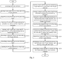
Fig. 1 shows a flow chart of a method of manufacturing the reverse conducting insulated gate bipolar transistor in an embodiment; -
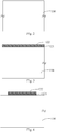
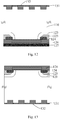
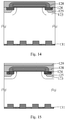
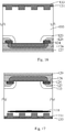
Figs. 2 to 17 are schematic diagrams of corresponding reverse conducting insulated gate bipolar transistor in the manufacturing method of the field stop insulated gate bipolar transistor shown inFig. 1 . - Referring to
Fig. 1 , in an embodiment, the method of manufacturing the reverse conducting insulated gate bipolar transistor is provided, which includes the following steps. - In step S111, an N-
type substrate 110 is prepared. As shown inFig. 2 , the N-type substrate 110 is an N-type silicon substrate. - In step S112, a
gate oxide layer 121 is grown at a front side of the N-type substrate 110. As shown inFig. 3 , the thickness of thegate oxide layer 121 is from 600 angstroms to 1500 angstroms. - In step S 113, a
poly silicon gate 122 is deposited on thegate oxide layer 121, as shown inFig. 3 . - In step S114, a
P well 123 is formed on the N-type substrate 110 by photoetching, etching and ion-implanting processes (referring toFig. 5 ). Referring toFig. 4 , an implantation window of theP well 123 is formed by selectively etching thepolysilicon gate 122 and thegate oxide layer 121 by the photoetching process. Referring toFig. 5 , a P-type impurity is implanted to the implantation window of theP well 123 by the self-aligned implantation process, and theP well 123 is formed by a drive-in process. - In step S115, an
N+ region 124 and a frontside P+ region 125 are formed in theP well 123 by photoetching and ion-implanting processes (referring toFig. 7 ). Referring toFig. 6 , ions are selectively implanted to theP well 123 by the photoetching process, and theN+ region 124 is formed by the drive-in process. Referring toFig. 7 , ions are selectively implanted to theP well 123 by the photoetching process, and the frontside P+ region 125 is formed by the drive-in process. The N+region 124 is mainly configured as an emitter of the reverse conducting insulated gate bipolar transistor. - In step S116, a
dielectric layer 126 is deposited at the front side of the N-type substrate 110. As shown inFig. 8 , thedielectric layer 126 is made of silicon dioxide and boro-phospho-silicate glass. - In step S 117, a protecting
layer 127 is deposited on thedielectric layer 126. As shown inFig. 9 , the protecting layer is made of silicon nitride. - In step S118, the N-
type substrate 110 is ground by a back side grinding process. In step 118, the N-type substrate 110 is ground to the required thickness. - In step S121, a back
side P+ region 131 is formed by implanting a P-type impurity to a back side of the N-type substrate 110, as shown inFig. 10 . - In step S122, a
trench 132 is formed at the back side of the N-type substrate 110 by photoetching and etching processes. As shown inFig. 11 , in the embodiment, thetrench 132 formed at the back side of the N-type substrate 110 is of a rectangle shape. Of course, thetrench 132 formed at the back side of the N-type substrate 110 is of a circle, an oval, a trapezium and other appropriate shapes. When thetrench 132 formed at the back side of the N-type substrate 110 is of a rectangle shape, a depth of thetrench 132 is from 1 to 20µm, a width thereof is from 1 to 30µm, and a distance between twoadjacent trenches 132 is from 50 to 300µm. - In step S123, the
trench 132 is filled by depositing poly silicon at the back side of the N-type substrate 110, and the polysilicon at an area outside of thetrench 132 is etched. As shown inFig. 12 , in step S123, the reverse conducting diode is formed by filling polysilicon in thetrench 132. The parameters of the reverse conducting diode at the back side of the manufactured reverse conducting insulated gate bipolar transistor can be adjusted by adjusting the doping concentration of polysilicon in thetrench 132, so that the difficulty of the adjusting process is low and it is easy to control the process. Therefore, the manufacturing difficulty of the reverse conducting insulated gate bipolar transistor can be reduced. Of course, the parameters of the reverse conducting diode at the back side of the reverse conducting insulated gate bipolar transistor can be also adjusted by adjusting a width and a depth of thetrench 132, or by adjusting the doping concentration of polysilicon in thetrench 132 and the width and the depth of thetrench 132 at the same time. Therefore, the difficulty of the adjusting process of the reverse conducting insulated gate bipolar transistor can be reduced, and then the manufacturing difficulty thereof is reduced. In the embodiment, the polysilicon deposited in thetrench 132 formed at the back side of the N-type substrate 110 is N-type polysilicon. The doping concentration of the polysilicon deposited in thetrench 132 is 1E17 to 1E21cm-3. - In step S124, the protecting
layer 127 at the front side of the N-type substrate is removed, as shown inFig. 13 . - In step S125, a contact hole for shorting the
N+ region 124 and the frontside P+ region 125 is formed by selectively etching thedielectric layer 126, and a frontside metal layer 128 is formed. As shown inFig. 14 , from the manufacturing flow of the reverse conducting insulated gate bipolar transistor described above, it can be understood that step S122 and step S123 are performed after performing step S116. In other words, forming thetrench 132 at the back side of the N-type substrate 110 and depositing the poly silicon in thetrench 132 are performed after performing depositing thedielectric layer 126 at the front side of the N-type substrate 110 rather than after performing the whole front side process of the reverse conducting insulated gate bipolar transistor. Such a manufacturing method has the following advantages. Firstly, after the P-type impurity is implanted at the back side of the N-type substrate 110 in step S121, the following front side thermal processes such as the hole reflow process (the hole reflow process is in forming the contact hole for shorting theN+ region 124 and the frontside P+ region 125 by selectively etching thedielectric layer 126 and forming a frontside metal layer 128 of step S125, and the temperature of the step S125 is about 850 degrees centigrade) and so on are performed. The activity of the P-type impurity at the back side of the N-type substrate 110 is very high without performing the annealing process individually. Therefore, the step of the thermal annealing of the P-type impurity at the back side of the N-type substrate 110 can be omitted. Further, the polysilicon in thetrench 123 at the back side of the N-type substrate 110 and the polysilicon of the front side are processed separately, thus easily controlling the doping concentration of the polysilicon. - In step S126, a
passivation layer 129 is deposited at the front side of the N-type substrate 110. As shown inFig. 15 , here, a pad area is formed by performing the etching process. - In step S127, a back
side metal layer 133 is formed by performing a back side metalized process at the back side of the N-type substrate 110. In the embodiment, from the N-type substrate to an external, the backside metal layer 133 at the back side of the N-type substrate 110 comprises aluminum, titanium, nickel and silver, which are laminated in that order. In other words, the outermost layer is metal silver. - In step S128, a carrier lifetime at a
partial area 111 in the N-type substrate 110 is controlled by a local radiation technique. As shown inFig. 17 , in the embodiment, the local radiation technique radiates the N-type substrate 110 by using electron or proton to control the life of the carrier at apartial area 111 in the N-type substrate 110. Therefore, manufacturing of the reverse conducting insulated gate bipolar transistor is completed. - The method of manufacturing the reverse conducting insulated gate bipolar transistor described above uses polysilicon for filling the trench at the back side of the reverse conducting insulated gate bipolar transistor. Thus, the parameters of the reverse conducting diode at the back side of the reverse conducting insulated gate bipolar transistor can be controlled by only precisely controlling the doping concentration of polysilicon, resulting in a lower requirement of controlling the process. Therefore, the method of manufacturing the reverse conducting insulated gate bipolar transistor has a lower requirement of controlling the manufacturing process, and a less difficulty of manufacturing.
- Although the invention is illustrated and described herein with reference to specific embodiments, the invention is not intended to be limited to the details shown. Rather, various modifications may be made in the details within the scope and range of equivalents of the claims and without departing from the invention.
Claims (10)
- A method of manufacturing a reverse conducting insulated gate bipolar transistor, comprising the following steps:preparing an N-type substrate;growing a gate oxide layer at a front side of the N-type substrate;depositing a polysilicon gate on the gate oxide layer;forming a P well on the N-type substrate by photoetching, etching and ion-implanting processes;forming an N+ region and a front side P+ region in the P well by photoetching and ion-implanting processes;depositing a dielectric layer at the front side of the N-type substrate;depositing a protecting layer on the dielectric layer;grinding the N-type substrate by a back side grinding process;forming a back side P+ region by implanting a P-type impurity to a back side of the N-type substrate;forming a trench at the back side of the N-type substrate by photoetching and etching processes;filling the trench by depositing polysilicon at the back side of the N-type substrate, and etching the polysilicon positioned at an area outside of the trench;removing the protecting layer at the front side of the N-type substrate;selectively etching the dielectric layer to form a contact hole for shorting the N+ region and the front side P+ region, and forming a front side metal layer;depositing a passivation layer at the front side of the N-type substrate; andperforming a back side metallization process at the back side of the N-type substrate, and forming a back side metal layer.
- The method of manufacturing the reverse conducting insulated gate bipolar transistor of claim 1, characterized in that, after forming the back side metal layer by performing the back side metalized process at the back side of the N-type substrate, the method further comprises controlling a carrier lifetime at a partial area in the N-type substrate by a local radiation technique.
- The method of manufacturing the reverse conducting insulated gate bipolar transistor of claim 2, characterized in that, the local radiation technique radiates the N-type substrate by using electron or proton.
- The method of manufacturing the reverse conducting insulated gate bipolar transistor of claim 1, characterized in that, the trench formed at the back side of the N-type substrate is of a rectangle shape.
- The method of manufacturing the reverse conducting insulated gate bipolar transistor of claim 4, characterized in that, a depth of the trench formed at the back side of the N-type substrate is from 1 to 20µm, a width thereof is from 1 to 30µm, and a distance between two adjacent trenches is from 50 to 300µm.
- The method of manufacturing the reverse conducting insulated gate bipolar transistor of claim 1, characterized in that, the polysilicon deposited in the trench formed at the back side of the N-type substrate is N-type polysilicon.
- The method of manufacturing the reverse conducting insulated gate bipolar transistor of claim 6, characterized in that, a doping concentration of the polysilicon deposited in the trench formed at the back side of the N-type substrate is 1E17 to 1E21cm-3.
- The method of manufacturing the reverse conducting insulated gate bipolar transistor of any one of claims 1 to 7, characterized in that, from the N-type substrate to an external, the back side metal layer comprises aluminum, titanium, nickel and silver, which are laminated in that order.
- The method of manufacturing the reverse conducting insulated gate bipolar transistor of any one of claims 1 to 7, characterized in that, the dielectric layer is made of silicon dioxide and boro-phospho-silicate glass.
- The method of manufacturing the reverse conducting insulated gate bipolar transistor of any one of claims 1 to 7, characterized in that, the protecting layer is made of silicon nitride.
Applications Claiming Priority (2)
| Application Number | Priority Date | Filing Date | Title |
|---|---|---|---|
| CN201310374240.3A CN104425245B (en) | 2013-08-23 | 2013-08-23 | Reverse-conducting insulated gate bipolar transistor npn npn manufacture method |
| PCT/CN2014/084720 WO2015024502A1 (en) | 2013-08-23 | 2014-08-19 | Manufacturing method for reverse conducting insulated gate bipolar transistor |
Publications (3)
| Publication Number | Publication Date |
|---|---|
| EP3002781A1 true EP3002781A1 (en) | 2016-04-06 |
| EP3002781A4 EP3002781A4 (en) | 2017-01-25 |
| EP3002781B1 EP3002781B1 (en) | 2019-10-09 |
Family
ID=52483081
Family Applications (1)
| Application Number | Title | Priority Date | Filing Date |
|---|---|---|---|
| EP14838639.4A Active EP3002781B1 (en) | 2013-08-23 | 2014-08-19 | Manufacturing method for reverse conducting insulated gate bipolar transistor |
Country Status (4)
| Country | Link |
|---|---|
| US (1) | US9673193B2 (en) |
| EP (1) | EP3002781B1 (en) |
| CN (1) | CN104425245B (en) |
| WO (1) | WO2015024502A1 (en) |
Families Citing this family (14)
| Publication number | Priority date | Publication date | Assignee | Title |
|---|---|---|---|---|
| CN104332494B (en) | 2013-07-22 | 2018-09-21 | 无锡华润上华科技有限公司 | A kind of igbt and its manufacturing method |
| CN104347401B (en) | 2013-07-29 | 2017-05-10 | 无锡华润上华半导体有限公司 | Manufacturing method of insulated gate bipolar transistor |
| CN104425246B (en) | 2013-08-27 | 2018-01-23 | 无锡华润上华科技有限公司 | Insulated gate bipolar transistor and preparation method thereof |
| CN104425259B (en) | 2013-09-02 | 2017-09-15 | 无锡华润上华半导体有限公司 | Reverse-conducting insulated gate bipolar transistor npn npn manufacture method |
| CN104701356B (en) | 2013-12-06 | 2018-01-12 | 无锡华润上华科技有限公司 | Semiconductor devices and preparation method thereof |
| CN104760925B (en) | 2014-01-07 | 2016-05-25 | 无锡华润上华半导体有限公司 | A kind of preparation method of film support beam |
| CN106298693A (en) * | 2015-05-13 | 2017-01-04 | 国网智能电网研究院 | A kind of manufacture method of high-voltage chip passivation layer |
| CN106483758B (en) | 2015-09-02 | 2019-08-20 | 无锡华润上华科技有限公司 | Optical proximity effect modification method and system |
| CN106653842B (en) | 2015-10-28 | 2019-05-17 | 无锡华润上华科技有限公司 | A semiconductor device with electrostatic discharge protection structure |
| CN106816468B (en) | 2015-11-30 | 2020-07-10 | 无锡华润上华科技有限公司 | Lateral diffusion metal oxide semiconductor field effect transistor with RESURF structure |
| CN107465983B (en) | 2016-06-03 | 2021-06-04 | 无锡华润上华科技有限公司 | MEMS microphone and preparation method thereof |
| CN116666210A (en) * | 2022-02-21 | 2023-08-29 | 珠海零边界集成电路有限公司 | Insulated gate bipolar transistor, manufacturing method, electronic device, and storage medium |
| CN116206958B (en) * | 2023-02-22 | 2026-03-31 | 马鞍山市槟城电子有限公司 | A method for fabricating a semiconductor device |
| CN119997524B (en) * | 2025-02-17 | 2025-11-18 | 上海爱廷电子科技有限公司 | FRD process control method with forward conduction voltage drop being positive in temperature characteristic |
Family Cites Families (20)
| Publication number | Priority date | Publication date | Assignee | Title |
|---|---|---|---|---|
| JPH03171777A (en) * | 1989-11-30 | 1991-07-25 | Toshiba Corp | Semiconductor device |
| US6482681B1 (en) * | 2000-05-05 | 2002-11-19 | International Rectifier Corporation | Hydrogen implant for buffer zone of punch-through non epi IGBT |
| JP2005057235A (en) * | 2003-07-24 | 2005-03-03 | Mitsubishi Electric Corp | Insulated gate bipolar transistor, method of manufacturing the same, and inverter circuit |
| JP4791704B2 (en) | 2004-04-28 | 2011-10-12 | 三菱電機株式会社 | Reverse conducting type semiconductor device and manufacturing method thereof |
| CN101060133A (en) * | 2006-03-16 | 2007-10-24 | 三洋电机株式会社 | Semiconductor device and manufacturing method thereof |
| US7557386B2 (en) * | 2006-03-30 | 2009-07-07 | Infineon Technologies Austria Ag | Reverse conducting IGBT with vertical carrier lifetime adjustment |
| JP2008117881A (en) * | 2006-11-02 | 2008-05-22 | Sanyo Electric Co Ltd | Semiconductor device and manufacturing method thereof |
| JP5150953B2 (en) * | 2008-01-23 | 2013-02-27 | 三菱電機株式会社 | Semiconductor device |
| JP2010003960A (en) * | 2008-06-23 | 2010-01-07 | Sanken Electric Co Ltd | Semiconductor device, and manufacturing method thereof |
| JP5587622B2 (en) * | 2010-01-27 | 2014-09-10 | ルネサスエレクトロニクス株式会社 | Reverse conduction type IGBT |
| DE112011100451T5 (en) * | 2010-02-04 | 2013-04-04 | Fuji Electric Co., Ltd | Method for producing a semiconductor device and device for producing a semiconductor device |
| CN103125023B (en) | 2011-09-28 | 2016-05-25 | 丰田自动车株式会社 | Semiconductor device and manufacture method thereof |
| CN103137472B (en) * | 2011-11-25 | 2016-06-08 | 上海华虹宏力半导体制造有限公司 | In conjunction with the fast IGBT device making method of pipe again |
| CN103035691B (en) * | 2012-03-12 | 2015-08-19 | 上海华虹宏力半导体制造有限公司 | Inverse conductivity type IGBT semiconductor device and manufacture method thereof |
| CN102916042B (en) * | 2012-09-28 | 2015-02-11 | 江苏物联网研究发展中心 | Reverse conduction IGBT device structure and manufacturing method |
| CN104332494B (en) | 2013-07-22 | 2018-09-21 | 无锡华润上华科技有限公司 | A kind of igbt and its manufacturing method |
| CN104347401B (en) | 2013-07-29 | 2017-05-10 | 无锡华润上华半导体有限公司 | Manufacturing method of insulated gate bipolar transistor |
| CN104425259B (en) | 2013-09-02 | 2017-09-15 | 无锡华润上华半导体有限公司 | Reverse-conducting insulated gate bipolar transistor npn npn manufacture method |
| CN104701356B (en) | 2013-12-06 | 2018-01-12 | 无锡华润上华科技有限公司 | Semiconductor devices and preparation method thereof |
| CN104760925B (en) | 2014-01-07 | 2016-05-25 | 无锡华润上华半导体有限公司 | A kind of preparation method of film support beam |
-
2013
- 2013-08-23 CN CN201310374240.3A patent/CN104425245B/en active Active
-
2014
- 2014-08-19 US US14/902,519 patent/US9673193B2/en active Active
- 2014-08-19 EP EP14838639.4A patent/EP3002781B1/en active Active
- 2014-08-19 WO PCT/CN2014/084720 patent/WO2015024502A1/en not_active Ceased
Also Published As
| Publication number | Publication date |
|---|---|
| US9673193B2 (en) | 2017-06-06 |
| CN104425245B (en) | 2017-11-07 |
| CN104425245A (en) | 2015-03-18 |
| EP3002781B1 (en) | 2019-10-09 |
| EP3002781A4 (en) | 2017-01-25 |
| WO2015024502A1 (en) | 2015-02-26 |
| US20160379974A1 (en) | 2016-12-29 |
Similar Documents
| Publication | Publication Date | Title |
|---|---|---|
| EP3002781B1 (en) | Manufacturing method for reverse conducting insulated gate bipolar transistor | |
| US12262553B2 (en) | Field stop IGBT with grown injection region | |
| CN105874607B (en) | The manufacturing method of semiconductor device and semiconductor device | |
| TWI553857B (en) | Semiconductor substrate structure, semiconductor power device, and injection control method for improving semiconductor power device | |
| US20130234201A1 (en) | Field stop structure, reverse conducting igbt semiconductor device and methods for manufacturing the same | |
| US8283213B2 (en) | Method of minimizing field stop insulated gate bipolar transistor (IGBT) buffer and emitter charge variation | |
| JP4128777B2 (en) | Insulated gate bipolar transistor (IGBT) and manufacturing method thereof | |
| JP2021073714A (en) | Semiconductor device and manufacturing method thereof | |
| CN110970485A (en) | Fast recovery diode structure controlled by carrier injection and manufacturing method thereof | |
| CN104253153B (en) | Field cut-off type reverse-conducting insulated gate bipolar transistor npn npn and its manufacture method | |
| CN103094324B (en) | Trench-type insulated gate bipolar transistor and preparation method thereof | |
| US7713794B2 (en) | Manufacturing method of a semiconductor device | |
| US8264036B2 (en) | Power semiconductor device with low on-state voltage and method of manufacturing the same | |
| US10096699B2 (en) | Field-stop reverse conducting insulated gate bipolar transistor and manufacturing method therefor | |
| CN103872108A (en) | IGBT structure and preparation method thereof | |
| CN106683989A (en) | Groove IGBT device and manufacturing method thereof | |
| US20160211258A1 (en) | Reverse-Conducting Gated-Base Bipolar-Conduction Devices and Methods with Reduced Risk of Warping | |
| US11264376B2 (en) | Bipolar semiconductor device and method for manufacturing such a semiconductor device | |
| CN106548938A (en) | Manufacturing method of semiconductor device | |
| WO2014154858A1 (en) | Method for manufacturing an insulated gate bipolar transistor | |
| CN104425578B (en) | Reverse Conducting Insulated Gate Bipolar Transistor | |
| US20240405108A1 (en) | Semiconductor device and method of manufacturing semiconductor device | |
| CN205508777U (en) | Semiconductor device | |
| US20250089307A1 (en) | Semiconductor device | |
| CN104253043A (en) | Field stop type insulated gate bipolar transistor manufacturing method |
Legal Events
| Date | Code | Title | Description |
|---|---|---|---|
| PUAI | Public reference made under article 153(3) epc to a published international application that has entered the european phase |
Free format text: ORIGINAL CODE: 0009012 |
|
| 17P | Request for examination filed |
Effective date: 20151230 |
|
| AK | Designated contracting states |
Kind code of ref document: A1 Designated state(s): AL AT BE BG CH CY CZ DE DK EE ES FI FR GB GR HR HU IE IS IT LI LT LU LV MC MK MT NL NO PL PT RO RS SE SI SK SM TR |
|
| AX | Request for extension of the european patent |
Extension state: BA ME |
|
| DAX | Request for extension of the european patent (deleted) | ||
| A4 | Supplementary search report drawn up and despatched |
Effective date: 20161222 |
|
| RIC1 | Information provided on ipc code assigned before grant |
Ipc: H01L 29/08 20060101ALI20161216BHEP Ipc: H01L 21/331 20060101AFI20161216BHEP Ipc: H01L 29/739 20060101ALI20161216BHEP Ipc: H01L 29/32 20060101ALI20161216BHEP |
|
| GRAP | Despatch of communication of intention to grant a patent |
Free format text: ORIGINAL CODE: EPIDOSNIGR1 |
|
| STAA | Information on the status of an ep patent application or granted ep patent |
Free format text: STATUS: GRANT OF PATENT IS INTENDED |
|
| INTG | Intention to grant announced |
Effective date: 20190418 |
|
| RAP1 | Party data changed (applicant data changed or rights of an application transferred) |
Owner name: CSMC TECHNOLOGIES FAB2 CO., LTD. |
|
| GRAS | Grant fee paid |
Free format text: ORIGINAL CODE: EPIDOSNIGR3 |
|
| GRAA | (expected) grant |
Free format text: ORIGINAL CODE: 0009210 |
|
| STAA | Information on the status of an ep patent application or granted ep patent |
Free format text: STATUS: THE PATENT HAS BEEN GRANTED |
|
| AK | Designated contracting states |
Kind code of ref document: B1 Designated state(s): AL AT BE BG CH CY CZ DE DK EE ES FI FR GB GR HR HU IE IS IT LI LT LU LV MC MK MT NL NO PL PT RO RS SE SI SK SM TR |
|
| REG | Reference to a national code |
Ref country code: GB Ref legal event code: FG4D |
|
| REG | Reference to a national code |
Ref country code: CH Ref legal event code: EP |
|
| REG | Reference to a national code |
Ref country code: IE Ref legal event code: FG4D |
|
| REG | Reference to a national code |
Ref country code: DE Ref legal event code: R096 Ref document number: 602014055033 Country of ref document: DE |
|
| REG | Reference to a national code |
Ref country code: AT Ref legal event code: REF Ref document number: 1189801 Country of ref document: AT Kind code of ref document: T Effective date: 20191115 |
|
| REG | Reference to a national code |
Ref country code: NL Ref legal event code: FP |
|
| REG | Reference to a national code |
Ref country code: LT Ref legal event code: MG4D |
|
| REG | Reference to a national code |
Ref country code: AT Ref legal event code: MK05 Ref document number: 1189801 Country of ref document: AT Kind code of ref document: T Effective date: 20191009 |
|
| PG25 | Lapsed in a contracting state [announced via postgrant information from national office to epo] |
Ref country code: AT Free format text: LAPSE BECAUSE OF FAILURE TO SUBMIT A TRANSLATION OF THE DESCRIPTION OR TO PAY THE FEE WITHIN THE PRESCRIBED TIME-LIMIT Effective date: 20191009 Ref country code: BG Free format text: LAPSE BECAUSE OF FAILURE TO SUBMIT A TRANSLATION OF THE DESCRIPTION OR TO PAY THE FEE WITHIN THE PRESCRIBED TIME-LIMIT Effective date: 20200109 Ref country code: FI Free format text: LAPSE BECAUSE OF FAILURE TO SUBMIT A TRANSLATION OF THE DESCRIPTION OR TO PAY THE FEE WITHIN THE PRESCRIBED TIME-LIMIT Effective date: 20191009 Ref country code: SE Free format text: LAPSE BECAUSE OF FAILURE TO SUBMIT A TRANSLATION OF THE DESCRIPTION OR TO PAY THE FEE WITHIN THE PRESCRIBED TIME-LIMIT Effective date: 20191009 Ref country code: LV Free format text: LAPSE BECAUSE OF FAILURE TO SUBMIT A TRANSLATION OF THE DESCRIPTION OR TO PAY THE FEE WITHIN THE PRESCRIBED TIME-LIMIT Effective date: 20191009 Ref country code: LT Free format text: LAPSE BECAUSE OF FAILURE TO SUBMIT A TRANSLATION OF THE DESCRIPTION OR TO PAY THE FEE WITHIN THE PRESCRIBED TIME-LIMIT Effective date: 20191009 Ref country code: PL Free format text: LAPSE BECAUSE OF FAILURE TO SUBMIT A TRANSLATION OF THE DESCRIPTION OR TO PAY THE FEE WITHIN THE PRESCRIBED TIME-LIMIT Effective date: 20191009 Ref country code: NO Free format text: LAPSE BECAUSE OF FAILURE TO SUBMIT A TRANSLATION OF THE DESCRIPTION OR TO PAY THE FEE WITHIN THE PRESCRIBED TIME-LIMIT Effective date: 20200109 Ref country code: PT Free format text: LAPSE BECAUSE OF FAILURE TO SUBMIT A TRANSLATION OF THE DESCRIPTION OR TO PAY THE FEE WITHIN THE PRESCRIBED TIME-LIMIT Effective date: 20200210 Ref country code: ES Free format text: LAPSE BECAUSE OF FAILURE TO SUBMIT A TRANSLATION OF THE DESCRIPTION OR TO PAY THE FEE WITHIN THE PRESCRIBED TIME-LIMIT Effective date: 20191009 Ref country code: GR Free format text: LAPSE BECAUSE OF FAILURE TO SUBMIT A TRANSLATION OF THE DESCRIPTION OR TO PAY THE FEE WITHIN THE PRESCRIBED TIME-LIMIT Effective date: 20200110 |
|
| PG25 | Lapsed in a contracting state [announced via postgrant information from national office to epo] |
Ref country code: HR Free format text: LAPSE BECAUSE OF FAILURE TO SUBMIT A TRANSLATION OF THE DESCRIPTION OR TO PAY THE FEE WITHIN THE PRESCRIBED TIME-LIMIT Effective date: 20191009 Ref country code: RS Free format text: LAPSE BECAUSE OF FAILURE TO SUBMIT A TRANSLATION OF THE DESCRIPTION OR TO PAY THE FEE WITHIN THE PRESCRIBED TIME-LIMIT Effective date: 20191009 Ref country code: IS Free format text: LAPSE BECAUSE OF FAILURE TO SUBMIT A TRANSLATION OF THE DESCRIPTION OR TO PAY THE FEE WITHIN THE PRESCRIBED TIME-LIMIT Effective date: 20200224 |
|
| PG25 | Lapsed in a contracting state [announced via postgrant information from national office to epo] |
Ref country code: AL Free format text: LAPSE BECAUSE OF FAILURE TO SUBMIT A TRANSLATION OF THE DESCRIPTION OR TO PAY THE FEE WITHIN THE PRESCRIBED TIME-LIMIT Effective date: 20191009 |
|
| REG | Reference to a national code |
Ref country code: DE Ref legal event code: R097 Ref document number: 602014055033 Country of ref document: DE |
|
| PG2D | Information on lapse in contracting state deleted |
Ref country code: IS |
|
| PG25 | Lapsed in a contracting state [announced via postgrant information from national office to epo] |
Ref country code: IS Free format text: LAPSE BECAUSE OF FAILURE TO SUBMIT A TRANSLATION OF THE DESCRIPTION OR TO PAY THE FEE WITHIN THE PRESCRIBED TIME-LIMIT Effective date: 20200209 Ref country code: RO Free format text: LAPSE BECAUSE OF FAILURE TO SUBMIT A TRANSLATION OF THE DESCRIPTION OR TO PAY THE FEE WITHIN THE PRESCRIBED TIME-LIMIT Effective date: 20191009 Ref country code: CZ Free format text: LAPSE BECAUSE OF FAILURE TO SUBMIT A TRANSLATION OF THE DESCRIPTION OR TO PAY THE FEE WITHIN THE PRESCRIBED TIME-LIMIT Effective date: 20191009 Ref country code: DK Free format text: LAPSE BECAUSE OF FAILURE TO SUBMIT A TRANSLATION OF THE DESCRIPTION OR TO PAY THE FEE WITHIN THE PRESCRIBED TIME-LIMIT Effective date: 20191009 Ref country code: EE Free format text: LAPSE BECAUSE OF FAILURE TO SUBMIT A TRANSLATION OF THE DESCRIPTION OR TO PAY THE FEE WITHIN THE PRESCRIBED TIME-LIMIT Effective date: 20191009 |
|
| PLBE | No opposition filed within time limit |
Free format text: ORIGINAL CODE: 0009261 |
|
| STAA | Information on the status of an ep patent application or granted ep patent |
Free format text: STATUS: NO OPPOSITION FILED WITHIN TIME LIMIT |
|
| PG25 | Lapsed in a contracting state [announced via postgrant information from national office to epo] |
Ref country code: SK Free format text: LAPSE BECAUSE OF FAILURE TO SUBMIT A TRANSLATION OF THE DESCRIPTION OR TO PAY THE FEE WITHIN THE PRESCRIBED TIME-LIMIT Effective date: 20191009 Ref country code: IT Free format text: LAPSE BECAUSE OF FAILURE TO SUBMIT A TRANSLATION OF THE DESCRIPTION OR TO PAY THE FEE WITHIN THE PRESCRIBED TIME-LIMIT Effective date: 20191009 Ref country code: SM Free format text: LAPSE BECAUSE OF FAILURE TO SUBMIT A TRANSLATION OF THE DESCRIPTION OR TO PAY THE FEE WITHIN THE PRESCRIBED TIME-LIMIT Effective date: 20191009 |
|
| 26N | No opposition filed |
Effective date: 20200710 |
|
| PG25 | Lapsed in a contracting state [announced via postgrant information from national office to epo] |
Ref country code: SI Free format text: LAPSE BECAUSE OF FAILURE TO SUBMIT A TRANSLATION OF THE DESCRIPTION OR TO PAY THE FEE WITHIN THE PRESCRIBED TIME-LIMIT Effective date: 20191009 |
|
| PG25 | Lapsed in a contracting state [announced via postgrant information from national office to epo] |
Ref country code: MC Free format text: LAPSE BECAUSE OF FAILURE TO SUBMIT A TRANSLATION OF THE DESCRIPTION OR TO PAY THE FEE WITHIN THE PRESCRIBED TIME-LIMIT Effective date: 20191009 |
|
| REG | Reference to a national code |
Ref country code: CH Ref legal event code: PL |
|
| PG25 | Lapsed in a contracting state [announced via postgrant information from national office to epo] |
Ref country code: LI Free format text: LAPSE BECAUSE OF NON-PAYMENT OF DUE FEES Effective date: 20200831 Ref country code: CH Free format text: LAPSE BECAUSE OF NON-PAYMENT OF DUE FEES Effective date: 20200831 Ref country code: LU Free format text: LAPSE BECAUSE OF NON-PAYMENT OF DUE FEES Effective date: 20200819 |
|
| REG | Reference to a national code |
Ref country code: BE Ref legal event code: MM Effective date: 20200831 |
|
| PG25 | Lapsed in a contracting state [announced via postgrant information from national office to epo] |
Ref country code: BE Free format text: LAPSE BECAUSE OF NON-PAYMENT OF DUE FEES Effective date: 20200831 Ref country code: IE Free format text: LAPSE BECAUSE OF NON-PAYMENT OF DUE FEES Effective date: 20200819 |
|
| PG25 | Lapsed in a contracting state [announced via postgrant information from national office to epo] |
Ref country code: TR Free format text: LAPSE BECAUSE OF FAILURE TO SUBMIT A TRANSLATION OF THE DESCRIPTION OR TO PAY THE FEE WITHIN THE PRESCRIBED TIME-LIMIT Effective date: 20191009 Ref country code: MT Free format text: LAPSE BECAUSE OF FAILURE TO SUBMIT A TRANSLATION OF THE DESCRIPTION OR TO PAY THE FEE WITHIN THE PRESCRIBED TIME-LIMIT Effective date: 20191009 Ref country code: CY Free format text: LAPSE BECAUSE OF FAILURE TO SUBMIT A TRANSLATION OF THE DESCRIPTION OR TO PAY THE FEE WITHIN THE PRESCRIBED TIME-LIMIT Effective date: 20191009 |
|
| PG25 | Lapsed in a contracting state [announced via postgrant information from national office to epo] |
Ref country code: MK Free format text: LAPSE BECAUSE OF FAILURE TO SUBMIT A TRANSLATION OF THE DESCRIPTION OR TO PAY THE FEE WITHIN THE PRESCRIBED TIME-LIMIT Effective date: 20191009 |
|
| REG | Reference to a national code |
Ref country code: DE Ref legal event code: R079 Ref document number: 602014055033 Country of ref document: DE Free format text: PREVIOUS MAIN CLASS: H01L0021331000 Ipc: H10D0012010000 |
|
| PGFP | Annual fee paid to national office [announced via postgrant information from national office to epo] |
Ref country code: NL Payment date: 20250821 Year of fee payment: 12 |
|
| PGFP | Annual fee paid to national office [announced via postgrant information from national office to epo] |
Ref country code: DE Payment date: 20250820 Year of fee payment: 12 |
|
| PGFP | Annual fee paid to national office [announced via postgrant information from national office to epo] |
Ref country code: GB Payment date: 20250821 Year of fee payment: 12 |
|
| PGFP | Annual fee paid to national office [announced via postgrant information from national office to epo] |
Ref country code: FR Payment date: 20250829 Year of fee payment: 12 |