EP3001567A1 - Phase tracker for a phase locked loop - Google Patents
Phase tracker for a phase locked loop Download PDFInfo
- Publication number
- EP3001567A1 EP3001567A1 EP15181478.7A EP15181478A EP3001567A1 EP 3001567 A1 EP3001567 A1 EP 3001567A1 EP 15181478 A EP15181478 A EP 15181478A EP 3001567 A1 EP3001567 A1 EP 3001567A1
- Authority
- EP
- European Patent Office
- Prior art keywords
- phase
- locked loop
- circuit
- phase locked
- signal
- Prior art date
- Legal status (The legal status is an assumption and is not a legal conclusion. Google has not performed a legal analysis and makes no representation as to the accuracy of the status listed.)
- Granted
Links
Images



Classifications
-
- H—ELECTRICITY
- H03—ELECTRONIC CIRCUITRY
- H03L—AUTOMATIC CONTROL, STARTING, SYNCHRONISATION OR STABILISATION OF GENERATORS OF ELECTRONIC OSCILLATIONS OR PULSES
- H03L7/00—Automatic control of frequency or phase; Synchronisation
- H03L7/06—Automatic control of frequency or phase; Synchronisation using a reference signal applied to a frequency- or phase-locked loop
- H03L7/08—Details of the phase-locked loop
- H03L7/085—Details of the phase-locked loop concerning mainly the frequency- or phase-detection arrangement including the filtering or amplification of its output signal
-
- G—PHYSICS
- G04—HOROLOGY
- G04F—TIME-INTERVAL MEASURING
- G04F10/00—Apparatus for measuring unknown time intervals by electric means
- G04F10/005—Time-to-digital converters [TDC]
-
- H—ELECTRICITY
- H03—ELECTRONIC CIRCUITRY
- H03L—AUTOMATIC CONTROL, STARTING, SYNCHRONISATION OR STABILISATION OF GENERATORS OF ELECTRONIC OSCILLATIONS OR PULSES
- H03L7/00—Automatic control of frequency or phase; Synchronisation
- H03L7/06—Automatic control of frequency or phase; Synchronisation using a reference signal applied to a frequency- or phase-locked loop
- H03L7/16—Indirect frequency synthesis, i.e. generating a desired one of a number of predetermined frequencies using a frequency- or phase-locked loop
- H03L7/18—Indirect frequency synthesis, i.e. generating a desired one of a number of predetermined frequencies using a frequency- or phase-locked loop using a frequency divider or counter in the loop
- H03L7/197—Indirect frequency synthesis, i.e. generating a desired one of a number of predetermined frequencies using a frequency- or phase-locked loop using a frequency divider or counter in the loop a time difference being used for locking the loop, the counter counting between numbers which are variable in time or the frequency divider dividing by a factor variable in time, e.g. for obtaining fractional frequency division
- H03L7/1974—Indirect frequency synthesis, i.e. generating a desired one of a number of predetermined frequencies using a frequency- or phase-locked loop using a frequency divider or counter in the loop a time difference being used for locking the loop, the counter counting between numbers which are variable in time or the frequency divider dividing by a factor variable in time, e.g. for obtaining fractional frequency division for fractional frequency division
- H03L7/1976—Indirect frequency synthesis, i.e. generating a desired one of a number of predetermined frequencies using a frequency- or phase-locked loop using a frequency divider or counter in the loop a time difference being used for locking the loop, the counter counting between numbers which are variable in time or the frequency divider dividing by a factor variable in time, e.g. for obtaining fractional frequency division for fractional frequency division using a phase accumulator for controlling the counter or frequency divider
Definitions
- Communication devices such as laptop computers, tablet computers, smart phones and personal digital assistants (PDAs) often employ phase locked loops in the modulation of data onto a carrier signal for subsequent transmission.
- An output phase thereof is typically known, and this known output phase is sometimes employed by other circuits in the communication device.
- a device and method are disclosed that are directed to a phase locked loop having a phase tracker circuit associated therewith.
- phase locked loop is a common circuit employed in many different applicants.
- phase locked loop circuits are used to generate local oscillator (LO) signals for use in up-converters in transmitter circuits and down-converters in receiver circuits.
- LO local oscillator
- Phase locked loop circuits are also often used in modulator circuits for phase and/or frequency modulation.
- a phase locked loop circuit operates to maintain a predetermined phase difference between an output phase (i.e., an oscillator phase) and a reference phase.
- an output phase i.e., an oscillator phase
- a type 2 phase locked loop which is a common phase locked loop circuit implementation
- the predetermined phase difference between a divided down oscillator phase and a reference phase is zero. If the phase locked loop is interrupted, for example, by programming the phase locked loop to a different channel frequency or a phase modulation, the phase of the output oscillator signal of the phase locked loop drifts away from the known phase value established by the reference phase. Therefore the absolute phase of the phase locked loop is no longer known after an interruption by other circuits which may expect a non-interrupted constant output frequency of the phase locked loop circuit.
- a spur cancellation circuit employs knowledge of the phase in operation.
- Some types of spur cancellation circuitry reduce spurs (also called interference signals) by determining a cancelling tone and adding the cancelling tone to a baseband signal in the digital domain that results in a spur reduction in the transmit signal. Determining the cancelling tone may include selecting a frequency and/or a phase thereof. Determining the proper cancelling tone often requires knowledge of the phase of the oscillation signal output from the phase locked loop. Thus an interruption in the phase locked loop that causes a phase drift in the output (oscillator) signal thus causes a degradation in the performance of other circuits such as the spur cancellation circuit.
- a spur cancellation circuit undergoes a recalibration procedure upon detection of an interruption, however, such a recalibration to ascertain the new phase (i.e., the spur phase) may take several hundred microseconds, which severely degrades performance of the communication device.
- a phase locked loop circuit may experience an interruption due to various circumstances.
- One circumstance that might lead to an interruption is when a phase locked loop is employed within a receiver circuit and experiences a change in channel frequency.
- the receiver may regularly change receive channels in accordance with a predetermined channel hopping scheme.
- a receiver may receive an instruction to change channels in response to channel quality data that indicates a present channel has insufficient quality (e.g., a signal-to-noise ratio (SNR) below a predetermined level).
- SNR signal-to-noise ratio
- a phase drift is a movement of a phase value of the output signal of a phase locked loop circuit away from a previously known phase value, for example, when the phase locked loop circuit was in a previously locked state.
- phase locked loop circuits are sometimes employed in time division duplex (TDD) architectures in which a transceiver has both receiver circuitry and transmitter circuitry that shares an antenna port by switching back and forth in accordance with predetermined time slots.
- TDD time division duplex
- the receiver circuitry and the transmitter circuitry operate on the same channel, the frequency of such circuits is not exactly the same.
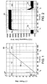
- Figs. 1 and 2 such figures illustrate how a phase drift in a phase locked loop can correspond to an interruption thereof. As illustrated in Fig.
- Fig. 1 that illustrates a phase drift that corresponds to the frequency change from RX to TX and back to RX, prior to t 1 a known phase 40 of about -7.5 exists, which is stable.
- the phase 50 between t 1 and t 2 drifts away from the previously known phase value to an unknown phase value.
- the phase 60 of the phase locked loop again stabilizes at 0.
- the absolute amount of phase drift depends upon the frequency offset between the receive and transmit modes, as well as the duration of the transmit mode. Because both of these factors are not known prior to design, as estimate of the phase drift experience by the phase locked loop problematic.
- the phase locked loop is being employed in a polar transmitter in a TDD type architecture, the phase locked loop is generating the phase modulated transmit signal.
- the phase information gets lost. So in such a situation the receiver circuitry uses the phase locked loop with no modulation, then the transmitter circuitry uses the phase locked loop with polar modulation, and then the receiver circuitry again uses the phase locked loop without modulation.
- the modulated phase results in a rising phase, but the rate of change in not constant and thus the phase is gain unknown.
- the present disclosure does not attempt to prevent interruptions or to prevent phase drift due to interruptions in a phase locked loop. Rather, the disclosure provides for a tracking circuit and method that operates to track the phase drift in real time and make the tracked phase drift available to other circuitry such as a spur cancellation circuit for use thereof, thereby avoiding time consuming and performance degrading recalibration procedures due to phase locked loop interruptions. While a spur cancellation circuit is highlighted as one example, it should be appreciated that other circuits may employ such information. For example, a digital signal processor algorithm may exploit this phase information for multiple different functions. Any subsequent use of the phase drift information may be utilized and all such implementations are contemplated as falling with the scope of the present disclosure.
- a phase locked loop 100 that includes a phase locked loop circuit 102 and a phase tracking circuit 104.
- the phase locked loop circuit 102 receives a reference signal 106 having a reference frequency and outputs an output signal 108 (also referred to as an oscillator signal) that is based on the reference frequency and a current channel word.
- the phase tracking circuit 104 is configured to determine a phase drift 110 based on a previous channel word and the current channel word of the phase locked loop circuit 102 (which may evidence an interruption thereof).
- the phase locked loop circuit 102 in one embodiment comprises a feedforward path 120 that receives the reference signal 106 having a reference frequency and outputs the output signal 108 having an output frequency.
- the feedforward path 120 comprises a time-to-digital converter (TDC) 122, a loop filter 124 and a digitally controlled oscillator (DCO) 126.
- the phase locked loop circuit 102 also comprises a feedback path 130 that includes a divider circuit 132.
- the divider circuit 132 receives the output (oscillator) signal 108 and generates a feedback signal 134 based thereon that comprises a divided down version of the output signal 108.
- the divider value (N) varies based on a divider control signal 136, which will be discussed in greater detail infra.
- the TDC 122 receives both the reference signal 106 and the feedback signal 134 and calculates a time difference between the respective phase of the received signals 106 and 134.
- the calculated time difference is output as a digital error value 140 and provided to the loop filter 124.
- the loop filter 124 receives the error signal 140 and outputs an oscillator control signal 142 in response thereto which controls an output frequency ( i.e., the output signal 108) of the controllable oscillator 126. More particularly, the control signal 142 output by the loop filter 124 results in a change in the output frequency of the output signal 108 such that a predetermined phase relationship is established and maintained between the reference signal 106 and the feedback signal 134.
- the desired phase relationship is identical phases, wherein the loop filter 124 alters the control signal 142 to minimize the error signal 140.
- the divide factor (N) of the divider circuit 132 is controlled via the divider control signal 136 that is output by a modulation circuit 150.
- the modulation circuit 150 receives modulation data and an intermediate (or new) channel word that in combination form a frequency control word 152 that operates to dictate changes in the divider control signal 136 that reflect a desired modulation of the output signal 108 of the phase locked loop circuit 102.
- the phase locked loop 100 further comprises the phase tracking circuit 104.
- the phase tracking circuit 104 receives the frequency control word 152 and a previous channel word 154, and based on the two input words 152 and 154 calculates an amount of phase drift 110 due to an interruption in the phase locked loop circuit 102.
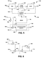
- Fig. 5 is another block diagram illustrating a phase locked loop circuit 102 having a phase tracking circuit 104 in accordance with another embodiment of the disclosure.
- the phase locked loop 100 has a phase locked loop circuit 102 similar to that illustrated in Fig. 4 , wherein a feedforward path 120 and a feedback path 130 operate to generate an output oscillator signal 108.
- the divider circuit 132 divides down the output signal 108 based on a divider control signal 136 provided by a MASH type modulator circuit 150.
- a MASH type modulator 150 is a variation of the general type delta-sigma modulator, commonly called a multi-stage noise shaping (MASH) structure that includes a noise shaping property.
- MASH multi-stage noise shaping
- the divide value N may comprise a fractional value.
- the MAH modulator comprises two more cascaded accumulator circuits, each of which is equivalent to a first-order sigma delta modulator.
- the divider circuit 132 may comprise a programmable multi-modulus divider (MMD), however, any type of divider circuit may be utilized.
- modulation data 160 and an intermediate (or new) channel word 162 are combined at first computation circuit (e.g ., an adder) 164 to form the frequency control word 152 that forms the input sequence to the MASH modulator 150.
- the frequency control word 152 is also input to a second computation circuit 166, wherein a difference 167 is computed between the frequency control word 152 and a previous control word 154 that represents the previous channel frequency. Therefore the frequency control word 152 contains information regarding the new channel frequency and the previous control word 154 contains information regarding the previous or old channel frequency.
- the resulting difference 167 represents a slope of the phase drift in the output signal 108.
- the difference signal 167 is input into an accumulator circuit 168, wherein the accumulation of the difference signal 167 over a time period represents the amount of phase drift through that time period ( i.e., signal 110).
- the amount of phase drift of the phase locked loop circuit will be a function both of the frequency offset and the duration of the offset.
- the frequency control word 152 contains information regarding the new channel frequency and the signal 154 contains information regarding the previous or old channel frequency.
- the difference signal 167 contains information relating to the size of the frequency offset between the old channel frequency and the new channel frequency.
- the resultant signal 110 contains information that reflects both the frequency offset as well as the duration of the frequency offset.
- Fig. 6 is a block diagram illustrating one example embodiment of an accumulator 168.
- the different signal 167 is input to a third computation circuit 172 that combines the difference signal 167 with a delayed version of the output signal 110 delayed through a delay unit 170 in a feedback path.
- the output signal 110 constitutes an accumulated signal that recursively adds the next amount of phase drift to a previous accumulated amount, thus continuously adding each of the elements of drift over a time period of the interruption to arrive at an accumulated value that represents the amount of phase drift 110 due to the interruption.
- the calculated phase drift 110 may then be used by other circuits that use knowledge of the phase of the phase locked loop circuit 102 in their respective functions.
- spur cancellation circuit uses knowledge of the phase in generating a calling tone. Since the amount of phase drift 110 has been calculated in real time, the phase drift signal 110 can be supplied as an input thereto and the spur cancellation circuit then has real time knowledge of the exact phase of the phase locked loop. Thus no time-consuming calibration procedure is necessary since the actual phase is known in real time due to the phase tracking circuit.
- phase characteristic will continue to drift over time due to repeating interruptions.
- a varying phase characteristic is illustrated in Figs. 7 and 8 .
- the accumulated phase can also become very high, which may require an accumulator such as the accumulator circuitry 168 of Figs. 5 and 6 to have a high bit width. While the present disclosure contemplates such an accumulator in one embodiment, a high bit width results in circuitry having a large amount of area and a large current consumption, which may be disadvantageous in some applications.
- a wraparound when the phase drift reaches 360 degrees.
- the frequency channel word e.g., defined by the output signal frequency divided by the reference frequency
- this is equivalent to a wraparound at 1.
- such a wraparound is illustrated in the accumulator circuit 168 of Fig. 9 .
- the difference value 167 is provided to the third computation circuit 172.
- the summation result in input to a truncation element 174 that operates to remove or otherwise ignore the integer portion so that only the fractional part of the channel word difference 167 is accumulated.
- an accumulator circuit 168 having a wraparound feature may be employed that does not require as significant a bit width.
- Fig. 10 is a flow chart illustrating a method 200 of operating a phase locked loop.
- the method 200 comprises generating an output signal of the phase locked loop (e.g., phase locked loop circuit 102 of Figs. 3-5 ) at 202, wherein the output signal has a known phase.
- the method 200 continues at 204 by tracking a phase drift of the output signal of the phase locked loop from the known phase due to an interruption of the phase locked loop.
- the interruption comprises a change in a channel frequency or a phase modulation of the output signal.
- a method of operating a phase locked loop is illustrated in Fig. 11 at reference numeral 300.
- the method 300 includes generating an output oscillator signal of a phase locked loop based on a reference signal having a reference frequency and a feedback signal having a feedback frequency at 302.
- a difference between a frequency control word that dictates a new divider value in the feedback path of the phase locked loop and a previous control word is calculated at 304.
- the frequency control word is a combination of modulation data and a new channel word.
- the calculated difference contains information related to a difference between the previous and new channel frequencies associated with an interruption of the circuit.
- the calculated differences between the frequency control word and the previous channel word are then accumulated over a period of time associated with the new channel frequency at 306.
- the accumulated differences correspond to an amount of phase drift of the output signal of the phase locked loop.
- the method 300 then continues at 308, wherein the determined phase drift of the output signal of the phase locked loop is employed by other circuits that employ knowledge of the output signal phase.
- a spur cancellation circuit is employed by other circuits that employ knowledge of the output signal phase.
- a method of operating a phase locked loop is provided. While the method provided herein is illustrated and described as a series of acts or events, the present disclosure is not limited by the illustrated ordering of such acts or events. For example, some acts may occur in different orders and/or concurrently with other acts or events apart from those illustrated and/or described herein. In addition, not all illustrated acts are required and the waveform shapes are merely illustrative and other waveforms may vary significantly from those illustrated. Further, one or more of the acts depicted herein may be carried out in one or more separate acts or phases.
- a phase locked loop comprises a phase locked loop circuit configured to output an output signal based on a reference frequency and a current channel word, and a phase tracking circuit.
- the phase tracking circuit is configured to determine a phase drift of the output signal based on a previous channel word and the current channel word of the phase locked loop circuit.
- the phase tracking circuit comprises an accumulator circuit that accumulates a difference between an input sequence and the previous channel word.
- the input sequence includes the current channel word and modulation data, and the accumulated difference represents the phase drift.
- the phase tracking circuit comprises a first calculation circuit configured to calculate a frequency control word based on the current channel word and modulation data, and a second calculation circuit configured to determine a difference between the frequency control word and the previous channel word.
- the difference represents a slope of the phase drift in the output signal.
- the phase tracking circuit further comprises an accumulator circuit configured to accumulate the difference representing the slope over a time period associated with an interruption of the output frequency. In one embodiment, the accumulated difference over the time period represents the phase drift of the output signal due to the interruption.
- the phase locked loop circuit comprises a feedforward path configured to receive a reference signal and a feedback signal, and output the output signal based thereon.
- the phase locked loop further comprises a feedback path comprising a divider circuit that receives the output signal and outputs the feedback signal based on a divider control signal that is a function of modulation data.
- the circuit comprises a feedforward path receiving a reference signal having a reference frequency and outputting an output signal having an output frequency that is a function of the reference signal and a feedback signal.
- the circuit further comprises a feedback path having a divider circuit associated therewith that is configured to receive the output signal and generate the feedback signal having a reduced frequency based on a divide value of the divider circuit.
- the feedback signal is supplied to the feedforward path.
- the circuit further comprises a modulator circuit configured to receive modulation data and provide a divider control signal to the divider circuit to control the divide value thereof, and a phase tracker circuit.
- the phase tracker circuit is configured to determine an amount of phase drift from an initial phase value of the output signal due to an interruption in a locked state of the phase locked loop.
- the phase tracker circuit is configured to determine the amount of phase drift from the initial phase value of the output signal due to an interruption using a modulation input sequence and a previous channel word.
- the modulation input sequence comprises modulation data and a new channel word that determines a new channel frequency of the phase locked loop.
- the phase tracker circuit comprises a first computation circuit configured to combine modulation data with a new channel control word to form a frequency control word for use by the modulator circuit, and a second computation circuit configured to determine a difference between the frequency control word and the previous channel word.
- the difference reflects a rate of change of phase drift.
- the phase tracker circuit further comprises an accumulator circuit configured to accumulate the difference output from the second computation circuit over a period of time, wherein an accumulated output of the differences from the second computation circuit represents an amount of phase drift from the initial phase value.
- the modulator circuit is configured to receive the frequency control word and generate the divider control signal in response thereto.
- the feedforward path comprises a time-to-digital converter (TDC) configured to receive the reference signal and the feedback signal, and output an error signal representing a difference in phase between the reference signal and the feedback signal.
- TDC time-to-digital converter
- the feedforward path further comprises a loop filter configured to receive the error signal and generate an oscillator control signal based thereon, and a controllable oscillator configured to receive the oscillator control signal and generate the output signal having an adjusted output frequency based thereon.
- the oscillator control signal is configured to minimize an amount of error in the error signal.
- the feedforward path further comprises an adder circuit between the loop filter and the controllable oscillator.
- the adder circuit is configured to combine the oscillator control signal and further modulation data to form a modulated oscillator control signal for control of the controllable oscillator.
- a method of operating a phase locked loop comprises generating an output signal of the phase locked loop, wherein the output signal has a known phase. The method further comprises tracking a phase drift of the output signal of the phase locked loop from the known phase due to an interruption of the phase locked loop.
- the interruption comprises a change in a channel frequency of the output signal or a phase modulation of the output signal.
- tracking the phase drift of the output signal comprises determining an amount of the phase drift based on a modulation input sequence and a previous channel word of the phase locked loop.
- the modulation input sequence comprises modulation data and a new channel word that dictates a new channel frequency of the phase locked loop.
- tracking the phase drift comprises combining modulation data with a new channel word to form a frequency control word, and determining a difference between the frequency control word and a previous channel word.
- the difference reflects a rate of change of phase drift.
- tracking the phase drift further comprise accumulating the difference over a period of time, wherein the accumulated differences represent an amount of phase drift from the known phase.
- a phase locked loop in one example of the disclosure, comprises a feedforward path receiving a reference signal having a reference frequency and outputting an output signal having an output frequency that is a function of the reference signal and a feedback signal.
- the phase locked loop also comprises a feedback path having a divider circuit associated therewith, and configured to receive the output signal and generate the feedback signal having a reduced frequency based on a divide value of the divider circuit, wherein the feedback signal is supplied to the feedforward path.
- the phase locked loop comprises a modulator circuit configured to receive modulation data and provide a divider control signal to the divider circuit to control the divide value thereof, and a means for phase tracking to determine an amount of phase drift from an initial phase value of the output signal due to an interruption in a locked state of the phase locked loop.
- the means for phase tracker circuit determines the amount of phase drift from the initial phase value of the output signal due to an interruption using a modulation input sequence and a previous channel word.
- the modulation input sequence comprises modulation data and a new channel word that determines a new channel frequency of the phase locked loop.
- the means for phase tracking comprises a first computation means to combine modulation data with a new channel control word to form a frequency control word for use by the modulator circuit and a second computation means to determine a difference between the frequency control word and the previous channel word, wherein the difference reflects a rate of change of phase drift.
- the means for phase tracking further comprises an accumulator means to accumulate the difference output from the second computation means over a period of time, wherein an accumulated output of the differences from the second computation means represents an amount of phase drift from the initial phase value.
- the accumulator means further comprises a truncation means to perform a wraparound function at an accumulated phase drift amount greater than 360 degrees.
- the truncation means performs the wraparound function by discarding integer portions of the accumulated output of the differences from the second computation circuit.
Landscapes
- Physics & Mathematics (AREA)
- General Physics & Mathematics (AREA)
- Stabilization Of Oscillater, Synchronisation, Frequency Synthesizers (AREA)
Abstract
Description
- Communication devices such as laptop computers, tablet computers, smart phones and personal digital assistants (PDAs) often employ phase locked loops in the modulation of data onto a carrier signal for subsequent transmission. An output phase thereof is typically known, and this known output phase is sometimes employed by other circuits in the communication device.
-
-
Fig. 1 is a graph illustrating a phase drift associated with an interruption in a phase locked loop circuit. -
Fig. 2 is a graph illustrating a frequency error cause by a change in channel frequency in a phase locked loop when transitioning between a receive mode and a transmit mode when a phase locked loop is a shared circuit in a time division duplexer (TDD) architecture. -
Fig. 3 is a block diagram illustrating a phase locked loop having a phase tracker in accordance with one embodiment of the disclosure. -
Fig. 4 is a block diagram illustrating a phase locked loop and modulation circuit having a phase tracker in accordance with another embodiment of the disclosure. -
Fig. 5 is a block diagram illustrating a phase locked loop having a phase tracker incorporating an accumulator circuit in accordance with another embodiment of the disclosure. -
Fig. 6 is a circuit diagram illustrating an accumulator circuit according to one embodiment of the disclosure. -
Fig. 7 is graph illustrating a phase drift associated with several interruptions in a phase locked loop circuit. -
Fig. 8 is a graph illustrating the impact on the phase along several changes in channel frequency in a phase locked loop when transitioning between a receive mode and a transmit mode when a phase locked loop is a shared circuit in a time division duplexer (TDD) architecture. -
Fig. 9 is a circuit diagram illustrating an accumulator circuit with a wraparound feature according to another embodiment of the disclosure. -
Fig. 10 is a flow chart illustrating a method of operating a phase locked loop that tracks a phase drift in an output frequency thereof according to one embodiment of the disclosure. -
Fig. 11 is a flow chart illustrating a method of operating a phase locked loop that tracks a phase drift in an output frequency thereof according to another embodiment of the disclosure. - The systems and methods of this disclosure are described with reference to the attached drawing figures, wherein like reference numerals are used to refer to like elements throughout, and wherein the illustrated structures and devices are not necessarily drawn to scale.
- A device and method are disclosed that are directed to a phase locked loop having a phase tracker circuit associated therewith.
- A phase locked loop is a common circuit employed in many different applicants. For example, in communications applications, phase locked loop circuits are used to generate local oscillator (LO) signals for use in up-converters in transmitter circuits and down-converters in receiver circuits. Phase locked loop circuits are also often used in modulator circuits for phase and/or frequency modulation.
- In general, a phase locked loop circuit operates to maintain a predetermined phase difference between an output phase (i.e., an oscillator phase) and a reference phase. In a
type 2 phase locked loop, which is a common phase locked loop circuit implementation, the predetermined phase difference between a divided down oscillator phase and a reference phase is zero. If the phase locked loop is interrupted, for example, by programming the phase locked loop to a different channel frequency or a phase modulation, the phase of the output oscillator signal of the phase locked loop drifts away from the known phase value established by the reference phase. Therefore the absolute phase of the phase locked loop is no longer known after an interruption by other circuits which may expect a non-interrupted constant output frequency of the phase locked loop circuit. - The loss of knowledge of the exact phase can be a problem with other circuits that use knowledge of the phase in its operation. In one non-limiting example, a spur cancellation circuit employs knowledge of the phase in operation. Some types of spur cancellation circuitry reduce spurs (also called interference signals) by determining a cancelling tone and adding the cancelling tone to a baseband signal in the digital domain that results in a spur reduction in the transmit signal. Determining the cancelling tone may include selecting a frequency and/or a phase thereof. Determining the proper cancelling tone often requires knowledge of the phase of the oscillation signal output from the phase locked loop. Thus an interruption in the phase locked loop that causes a phase drift in the output (oscillator) signal thus causes a degradation in the performance of other circuits such as the spur cancellation circuit. Conventionally, a spur cancellation circuit undergoes a recalibration procedure upon detection of an interruption, however, such a recalibration to ascertain the new phase (i.e., the spur phase) may take several hundred microseconds, which severely degrades performance of the communication device.
- A phase locked loop circuit may experience an interruption due to various circumstances. One circumstance that might lead to an interruption is when a phase locked loop is employed within a receiver circuit and experiences a change in channel frequency. For example, the receiver may regularly change receive channels in accordance with a predetermined channel hopping scheme. Alternatively, a receiver may receive an instruction to change channels in response to channel quality data that indicates a present channel has insufficient quality (e.g., a signal-to-noise ratio (SNR) below a predetermined level). In any event, even if subsequently the receiver switches back to the original channel relatively quickly (e.g., RX(f1) -> RX(f2) -> RX(f1), an interruption causes a phase drift. A phase drift is a movement of a phase value of the output signal of a phase locked loop circuit away from a previously known phase value, for example, when the phase locked loop circuit was in a previously locked state.
- In another example, phase locked loop circuits are sometimes employed in time division duplex (TDD) architectures in which a transceiver has both receiver circuitry and transmitter circuitry that shares an antenna port by switching back and forth in accordance with predetermined time slots. In such instances, while the receiver circuitry and the transmitter circuitry operate on the same channel, the frequency of such circuits is not exactly the same. For example, referring to
Figs. 1 and 2 , such figures illustrate how a phase drift in a phase locked loop can correspond to an interruption thereof. As illustrated inFig. 2 , a TDD architecture results in a receiver circuitry (RX) operating at a receive frequency 10 (illustrated as 0 frequency error) and then switching over to the transmit frequency at time t1 = 25 microseconds, wherein thetransmit frequency 20 is about 4kHz greater than the receiver operating frequency. The transmitter operates at such frequency until time t2 = 130 microseconds, at which time the receiver again begins operating at its original receive frequency at 30. As can be seen inFig. 1 that illustrates a phase drift that corresponds to the frequency change from RX to TX and back to RX, prior to t1 a knownphase 40 of about -7.5 exists, which is stable. Upon the interruption caused by the switch over to transmit, thephase 50 between t1 and t2 drifts away from the previously known phase value to an unknown phase value. Upon the change back to receive mode, thephase 60 of the phase locked loop again stabilizes at 0. - As can be seen in
Fig.1 , the absolute amount of phase drift depends upon the frequency offset between the receive and transmit modes, as well as the duration of the transmit mode. Because both of these factors are not known prior to design, as estimate of the phase drift experience by the phase locked loop problematic. - In another example, if the phase locked loop is being employed in a polar transmitter in a TDD type architecture, the phase locked loop is generating the phase modulated transmit signal. Thus when being shared by the receiver circuitry, the phase information gets lost. So in such a situation the receiver circuitry uses the phase locked loop with no modulation, then the transmitter circuitry uses the phase locked loop with polar modulation, and then the receiver circuitry again uses the phase locked loop without modulation. Thus in such a TDD based polar modulator transmitter scheme when the phase locked loop circuit is being shared by both the receive and transmit chains to reduce power consumption the modulated phase results in a rising phase, but the rate of change in not constant and thus the phase is gain unknown.
- The present disclosure does not attempt to prevent interruptions or to prevent phase drift due to interruptions in a phase locked loop. Rather, the disclosure provides for a tracking circuit and method that operates to track the phase drift in real time and make the tracked phase drift available to other circuitry such as a spur cancellation circuit for use thereof, thereby avoiding time consuming and performance degrading recalibration procedures due to phase locked loop interruptions. While a spur cancellation circuit is highlighted as one example, it should be appreciated that other circuits may employ such information. For example, a digital signal processor algorithm may exploit this phase information for multiple different functions. Any subsequent use of the phase drift information may be utilized and all such implementations are contemplated as falling with the scope of the present disclosure.
- Turning now to
Fig. 3 , a phase lockedloop 100 is provided that includes a phase lockedloop circuit 102 and aphase tracking circuit 104. The phase lockedloop circuit 102 receives areference signal 106 having a reference frequency and outputs an output signal 108 (also referred to as an oscillator signal) that is based on the reference frequency and a current channel word. Thephase tracking circuit 104 is configured to determine aphase drift 110 based on a previous channel word and the current channel word of the phase locked loop circuit 102 (which may evidence an interruption thereof). - Another embodiment of the disclosure is illustrated in
Fig. 4 . The phase lockedloop circuit 102 in one embodiment comprises afeedforward path 120 that receives thereference signal 106 having a reference frequency and outputs theoutput signal 108 having an output frequency. In one embodiment thefeedforward path 120 comprises a time-to-digital converter (TDC) 122, aloop filter 124 and a digitally controlled oscillator (DCO) 126. The phase lockedloop circuit 102 also comprises afeedback path 130 that includes adivider circuit 132. Thedivider circuit 132 receives the output (oscillator)signal 108 and generates afeedback signal 134 based thereon that comprises a divided down version of theoutput signal 108. The divider value (N) varies based on adivider control signal 136, which will be discussed in greater detail infra. - Referring again to the
feedforward path 120 of the phase lockedloop circuit 102, theTDC 122 receives both thereference signal 106 and thefeedback signal 134 and calculates a time difference between the respective phase of the receivedsignals digital error value 140 and provided to theloop filter 124. Theloop filter 124 receives theerror signal 140 and outputs anoscillator control signal 142 in response thereto which controls an output frequency (i.e., the output signal 108) of thecontrollable oscillator 126. More particularly, thecontrol signal 142 output by theloop filter 124 results in a change in the output frequency of theoutput signal 108 such that a predetermined phase relationship is established and maintained between thereference signal 106 and thefeedback signal 134. In one embodiment the desired phase relationship is identical phases, wherein theloop filter 124 alters thecontrol signal 142 to minimize theerror signal 140. - As highlighted above, the divide factor (N) of the
divider circuit 132 is controlled via thedivider control signal 136 that is output by amodulation circuit 150. Themodulation circuit 150 receives modulation data and an intermediate (or new) channel word that in combination form afrequency control word 152 that operates to dictate changes in thedivider control signal 136 that reflect a desired modulation of theoutput signal 108 of the phase lockedloop circuit 102. - Still referring to
Fig. 4 , the phase lockedloop 100 further comprises thephase tracking circuit 104. Thephase tracking circuit 104 receives thefrequency control word 152 and aprevious channel word 154, and based on the twoinput words phase drift 110 due to an interruption in the phase lockedloop circuit 102. -
Fig. 5 is another block diagram illustrating a phase lockedloop circuit 102 having aphase tracking circuit 104 in accordance with another embodiment of the disclosure. The phase lockedloop 100 has a phase lockedloop circuit 102 similar to that illustrated inFig. 4 , wherein afeedforward path 120 and afeedback path 130 operate to generate anoutput oscillator signal 108. Thedivider circuit 132 divides down theoutput signal 108 based on adivider control signal 136 provided by a MASHtype modulator circuit 150. In one embodiment aMASH type modulator 150 is a variation of the general type delta-sigma modulator, commonly called a multi-stage noise shaping (MASH) structure that includes a noise shaping property. Such a structure is often used in fractional-N phase locked loops, wherein the divide value N may comprise a fractional value. In one example, the MAH modulator comprises two more cascaded accumulator circuits, each of which is equivalent to a first-order sigma delta modulator. However, other type modulator circuits may be employed and all such variations are contemplated as falling within the scope of the present disclosure. In addition, on one embodiment, thedivider circuit 132 may comprise a programmable multi-modulus divider (MMD), however, any type of divider circuit may be utilized. - Still referring to
Fig. 5 ,modulation data 160 and an intermediate (or new)channel word 162 are combined at first computation circuit (e.g., an adder) 164 to form thefrequency control word 152 that forms the input sequence to theMASH modulator 150. Thefrequency control word 152 is also input to asecond computation circuit 166, wherein adifference 167 is computed between thefrequency control word 152 and aprevious control word 154 that represents the previous channel frequency. Therefore thefrequency control word 152 contains information regarding the new channel frequency and theprevious control word 154 contains information regarding the previous or old channel frequency. The resultingdifference 167 represents a slope of the phase drift in theoutput signal 108. Thedifference signal 167 is input into anaccumulator circuit 168, wherein the accumulation of thedifference signal 167 over a time period represents the amount of phase drift through that time period (i.e., signal 110). - As previously discussed in conjunction with
Figs. 1 and 2 , the amount of phase drift of the phase locked loop circuit will be a function both of the frequency offset and the duration of the offset. As seen inFig. 5 , thefrequency control word 152 contains information regarding the new channel frequency and thesignal 154 contains information regarding the previous or old channel frequency. Thus thedifference signal 167 contains information relating to the size of the frequency offset between the old channel frequency and the new channel frequency. Further, by accumulating the difference over the entire time period of the interruption, theresultant signal 110 contains information that reflects both the frequency offset as well as the duration of the frequency offset. -
Fig. 6 is a block diagram illustrating one example embodiment of anaccumulator 168. As illustrated, thedifferent signal 167 is input to athird computation circuit 172 that combines thedifference signal 167 with a delayed version of theoutput signal 110 delayed through adelay unit 170 in a feedback path. Thus theoutput signal 110 constitutes an accumulated signal that recursively adds the next amount of phase drift to a previous accumulated amount, thus continuously adding each of the elements of drift over a time period of the interruption to arrive at an accumulated value that represents the amount ofphase drift 110 due to the interruption. Thecalculated phase drift 110 may then be used by other circuits that use knowledge of the phase of the phase lockedloop circuit 102 in their respective functions. For example, as discussed previously, spur cancellation circuit uses knowledge of the phase in generating a calling tone. Since the amount ofphase drift 110 has been calculated in real time, thephase drift signal 110 can be supplied as an input thereto and the spur cancellation circuit then has real time knowledge of the exact phase of the phase locked loop. Thus no time-consuming calibration procedure is necessary since the actual phase is known in real time due to the phase tracking circuit. - The phase characteristic will continue to drift over time due to repeating interruptions. One further example of a varying phase characteristic is illustrated in
Figs. 7 and 8 . As can be appreciated, the accumulated phase can also become very high, which may require an accumulator such as theaccumulator circuitry 168 ofFigs. 5 and 6 to have a high bit width. While the present disclosure contemplates such an accumulator in one embodiment, a high bit width results in circuitry having a large amount of area and a large current consumption, which may be disadvantageous in some applications. - For many applications it is sufficient to do a wraparound when the phase drift reaches 360 degrees. For the frequency channel word (e.g., defined by the output signal frequency divided by the reference frequency), this is equivalent to a wraparound at 1. In one embodiment of the disclosure, such a wraparound is illustrated in the
accumulator circuit 168 ofFig. 9 . As shown inFig. 9 , thedifference value 167 is provided to thethird computation circuit 172. The summation result in input to atruncation element 174 that operates to remove or otherwise ignore the integer portion so that only the fractional part of thechannel word difference 167 is accumulated. In the above manner, anaccumulator circuit 168 having a wraparound feature may be employed that does not require as significant a bit width. -
Fig. 10 is a flow chart illustrating amethod 200 of operating a phase locked loop. Themethod 200 comprises generating an output signal of the phase locked loop (e.g., phase lockedloop circuit 102 ofFigs. 3-5 ) at 202, wherein the output signal has a known phase. Themethod 200 continues at 204 by tracking a phase drift of the output signal of the phase locked loop from the known phase due to an interruption of the phase locked loop. According to one embodiment the interruption comprises a change in a channel frequency or a phase modulation of the output signal. - According to another embodiment, a method of operating a phase locked loop is illustrated in
Fig. 11 atreference numeral 300. Themethod 300 includes generating an output oscillator signal of a phase locked loop based on a reference signal having a reference frequency and a feedback signal having a feedback frequency at 302. A difference between a frequency control word that dictates a new divider value in the feedback path of the phase locked loop and a previous control word is calculated at 304. In one embodiment the frequency control word is a combination of modulation data and a new channel word. - In one embodiment, the calculated difference contains information related to a difference between the previous and new channel frequencies associated with an interruption of the circuit. The calculated differences between the frequency control word and the previous channel word are then accumulated over a period of time associated with the new channel frequency at 306. The accumulated differences correspond to an amount of phase drift of the output signal of the phase locked loop. The
method 300 then continues at 308, wherein the determined phase drift of the output signal of the phase locked loop is employed by other circuits that employ knowledge of the output signal phase. One example of such a circuit is a spur cancellation circuit. - In another embodiment of the disclosure, a method of operating a phase locked loop is provided. While the method provided herein is illustrated and described as a series of acts or events, the present disclosure is not limited by the illustrated ordering of such acts or events. For example, some acts may occur in different orders and/or concurrently with other acts or events apart from those illustrated and/or described herein. In addition, not all illustrated acts are required and the waveform shapes are merely illustrative and other waveforms may vary significantly from those illustrated. Further, one or more of the acts depicted herein may be carried out in one or more separate acts or phases.
- In one example a phase locked loop comprises a phase locked loop circuit configured to output an output signal based on a reference frequency and a current channel word, and a phase tracking circuit. The phase tracking circuit is configured to determine a phase drift of the output signal based on a previous channel word and the current channel word of the phase locked loop circuit.
- In one example of the phase locked loop, the phase tracking circuit comprises an accumulator circuit that accumulates a difference between an input sequence and the previous channel word. In one embodiment, the input sequence includes the current channel word and modulation data, and the accumulated difference represents the phase drift.
- In one example of the phase locked loop circuit, the phase tracking circuit comprises a first calculation circuit configured to calculate a frequency control word based on the current channel word and modulation data, and a second calculation circuit configured to determine a difference between the frequency control word and the previous channel word. In one embodiment, the difference represents a slope of the phase drift in the output signal. The phase tracking circuit further comprises an accumulator circuit configured to accumulate the difference representing the slope over a time period associated with an interruption of the output frequency. In one embodiment, the accumulated difference over the time period represents the phase drift of the output signal due to the interruption.
- In one example of the phase locked loop, the phase locked loop circuit comprises a feedforward path configured to receive a reference signal and a feedback signal, and output the output signal based thereon. The phase locked loop further comprises a feedback path comprising a divider circuit that receives the output signal and outputs the feedback signal based on a divider control signal that is a function of modulation data.
- In one example of the phase locked loop, the circuit comprises a feedforward path receiving a reference signal having a reference frequency and outputting an output signal having an output frequency that is a function of the reference signal and a feedback signal. The circuit further comprises a feedback path having a divider circuit associated therewith that is configured to receive the output signal and generate the feedback signal having a reduced frequency based on a divide value of the divider circuit. The feedback signal is supplied to the feedforward path. The circuit further comprises a modulator circuit configured to receive modulation data and provide a divider control signal to the divider circuit to control the divide value thereof, and a phase tracker circuit. The phase tracker circuit is configured to determine an amount of phase drift from an initial phase value of the output signal due to an interruption in a locked state of the phase locked loop.
- In one example of the phase locked loop, the phase tracker circuit is configured to determine the amount of phase drift from the initial phase value of the output signal due to an interruption using a modulation input sequence and a previous channel word.
- In one example of the phase locked loop, the modulation input sequence comprises modulation data and a new channel word that determines a new channel frequency of the phase locked loop.
- In one example of the phase locked loop, the phase tracker circuit comprises a first computation circuit configured to combine modulation data with a new channel control word to form a frequency control word for use by the modulator circuit, and a second computation circuit configured to determine a difference between the frequency control word and the previous channel word. In one embodiment, the difference reflects a rate of change of phase drift.
- In one example of the phase locked loop, the phase tracker circuit further comprises an accumulator circuit configured to accumulate the difference output from the second computation circuit over a period of time, wherein an accumulated output of the differences from the second computation circuit represents an amount of phase drift from the initial phase value.
- In one example of the phase locked loop, the modulator circuit is configured to receive the frequency control word and generate the divider control signal in response thereto.
- In one example of the phase locked loop, the feedforward path comprises a time-to-digital converter (TDC) configured to receive the reference signal and the feedback signal, and output an error signal representing a difference in phase between the reference signal and the feedback signal.
- In one example of the phase locked loop, the feedforward path further comprises a loop filter configured to receive the error signal and generate an oscillator control signal based thereon, and a controllable oscillator configured to receive the oscillator control signal and generate the output signal having an adjusted output frequency based thereon. The oscillator control signal is configured to minimize an amount of error in the error signal.
- In one example of the phase locked loop, the feedforward path further comprises an adder circuit between the loop filter and the controllable oscillator. In one embodiment, the adder circuit is configured to combine the oscillator control signal and further modulation data to form a modulated oscillator control signal for control of the controllable oscillator.
- In one example, a method of operating a phase locked loop comprises generating an output signal of the phase locked loop, wherein the output signal has a known phase. The method further comprises tracking a phase drift of the output signal of the phase locked loop from the known phase due to an interruption of the phase locked loop.
- In one example of the method, the interruption comprises a change in a channel frequency of the output signal or a phase modulation of the output signal.
- In one example of the method, tracking the phase drift of the output signal comprises determining an amount of the phase drift based on a modulation input sequence and a previous channel word of the phase locked loop.
- In one example of the method, the modulation input sequence comprises modulation data and a new channel word that dictates a new channel frequency of the phase locked loop.
- In one example of the method, tracking the phase drift comprises combining modulation data with a new channel word to form a frequency control word, and determining a difference between the frequency control word and a previous channel word. In one embodiment, the difference reflects a rate of change of phase drift.
- In one example of the method, tracking the phase drift further comprise accumulating the difference over a period of time, wherein the accumulated differences represent an amount of phase drift from the known phase.
- In one example of the disclosure, a phase locked loop is disclosed, and comprises a feedforward path receiving a reference signal having a reference frequency and outputting an output signal having an output frequency that is a function of the reference signal and a feedback signal. The phase locked loop also comprises a feedback path having a divider circuit associated therewith, and configured to receive the output signal and generate the feedback signal having a reduced frequency based on a divide value of the divider circuit, wherein the feedback signal is supplied to the feedforward path. Further, the phase locked loop comprises a modulator circuit configured to receive modulation data and provide a divider control signal to the divider circuit to control the divide value thereof, and a means for phase tracking to determine an amount of phase drift from an initial phase value of the output signal due to an interruption in a locked state of the phase locked loop.
- In another example of the phase locked loop, the means for phase tracker circuit determines the amount of phase drift from the initial phase value of the output signal due to an interruption using a modulation input sequence and a previous channel word.
- In another example of the phase locked loop, the modulation input sequence comprises modulation data and a new channel word that determines a new channel frequency of the phase locked loop.
- In another example of the phase locked loop, the means for phase tracking comprises a first computation means to combine modulation data with a new channel control word to form a frequency control word for use by the modulator circuit and a second computation means to determine a difference between the frequency control word and the previous channel word, wherein the difference reflects a rate of change of phase drift.
- In another example of the phase locked loop, the means for phase tracking further comprises an accumulator means to accumulate the difference output from the second computation means over a period of time, wherein an accumulated output of the differences from the second computation means represents an amount of phase drift from the initial phase value.
- In another example of the phase locked loop, the accumulator means further comprises a truncation means to perform a wraparound function at an accumulated phase drift amount greater than 360 degrees.
- In another example of the phase locked loop, the truncation means performs the wraparound function by discarding integer portions of the accumulated output of the differences from the second computation circuit.
- It should be understood that all the circuits, components, units and other type elements disclosed herein can be employed solely in hardware, solely in software, or in a combination of hardware and software, and all such permutations are contemplated as falling within the scope of the present disclosure.
- It should be understood that although various examples are described separately above for purposes of clarity and brevity, various features of the various examples may be combined and all such combinations and permutations of such examples is expressly contemplated as falling within the scope of the present disclosure.
- Although the disclosure has been illustrated and described with respect to one or more implementations, alterations and/or modifications may be made to the illustrated examples without departing from the spirit and scope of the appended claims. Furthermore, in particular regard to the various functions performed by the above described components or structures (assemblies, devices, circuits, systems, etc.), the terms (including a reference to a "means") used to describe such components are intended to correspond, unless otherwise indicated, to any component or structure which performs the specified function of the described component (e.g., that is functionally equivalent), even though not structurally equivalent to the disclosed structure which performs the function in the herein illustrated exemplary implementations of the invention. In addition, while a particular feature of the disclosure may have been disclosed with respect to only one of several implementations, such feature may be combined with one or more other features of the other implementations as may be desired and advantageous for any given or particular application. Furthermore, to the extent that the terms "including", "includes", "having", "has", "with", or variants thereof are used in either the detailed description and the claims, such terms are intended to be inclusive in a manner similar to the term "comprising".
Claims (15)
- A phase locked loop, comprising:a feedforward path receiving a reference signal having a reference frequency and outputting an output signal having an output frequency that is a function of the reference signal and a feedback signal;;a feedback path having a divider circuit associated therewith, and configured to receive the output signal and generate the feedback signal having a reduced frequency based on a divide value of the divider circuit, wherein the feedback signal is supplied to the feedforward path;a modulator circuit configured to receive modulation data and provide a divider control signal to the divider circuit to control the divide value thereof; anda phase tracker circuit configured to determine an amount of phase drift from an initial phase value of the output signal due to an interruption in a locked state of the phase locked loop.
- The phase locked loop of claim 1, wherein the phase tracker circuit is configured to determine the amount of phase drift from the initial phase value of the output signal due to an interruption using a modulation input sequence and a previous channel word.
- The phase locked loop of claim 2, wherein the modulation input sequence comprises modulation data and a new channel word that determines a new channel frequency of the phase locked loop.
- The phase locked loop of claims 2 or 3, wherein the phase tracker circuit comprises:a first computation circuit configured to combine modulation data with a new channel control word to form a frequency control word for use by the modulator circuit; anda second computation circuit configured to determine a difference between the frequency control word and the previous channel word, wherein the difference reflects a rate of change of phase drift.
- The phase locked loop of claim 4, wherein the phase tracker circuit further comprises an accumulator circuit configured to accumulate the difference output from the second computation circuit over a period of time, wherein an accumulated output of the differences from the second computation circuit represents an amount of phase drift from the initial phase value.
- The phase locked loop of claim 5, wherein the accumulator circuit further comprises a truncation circuit configured to perform a wraparound function at an accumulated phase drift amount greater than 360 degrees.
- The phase locked loop of claim 6, wherein the truncation circuit is configured to perform the wraparound function by discarding integer portions of the accumulated output of the differences from the second computation circuit.
- The phase locked loop of any of claims 2-4, wherein the modulator circuit is configured to receive the frequency control word and generate the divider control signal in response thereto.
- The phase locked loop of any of claims 1-8, wherein the feedforward path comprises a time-to-digital converter (TDC) configured to receive the reference signal and the feedback signal, and output an error signal representing a difference in phase between the reference signal and the feedback signal.
- The phase locked loop of claim 9, wherein the feedforward path further comprises:a loop filter configured to receive the error signal and generate an oscillator control signal based thereon; anda controllable oscillator configured to receive the oscillator control signal and generate the output signal having an adjusted output frequency based thereon,wherein the oscillator control signal is configured to minimize an amount of error in the error signal.
- A method of operating a phase locked loop, comprising:generating an output signal of the phase locked loop, the output signal having a known phase; andtracking a phase drift of the output signal of the phase locked loop from the known phase due to an interruption of the phase locked loop.
- The method of claim 11, wherein the interruption comprises a change in a channel frequency of the output signal or a phase modulation of the output signal.
- The method of claims 11 or 12, wherein tracking the phase drift of the output signal comprises determining an amount of the phase drift based on a modulation input sequence and a previous channel word of the phase locked loop.
- The method of claim 13, wherein the modulation input sequence comprises modulation data and a new channel word that dictates a new channel frequency of the phase locked loop.
- The method of claims 11 or 12, wherein tracking the phase drift comprises:combining modulation data with a new channel word to form a frequency control word;determining a difference between the frequency control word and a previous channel word, wherein the difference reflects a rate of change of phase drift; andaccumulating the difference over a period of time, wherein the accumulated differences represent an amount of phase drift from the known phase.
Applications Claiming Priority (1)
| Application Number | Priority Date | Filing Date | Title |
|---|---|---|---|
| US14/494,718 US9584139B2 (en) | 2014-09-24 | 2014-09-24 | Phase tracker for a phase locked loop |
Publications (2)
| Publication Number | Publication Date |
|---|---|
| EP3001567A1 true EP3001567A1 (en) | 2016-03-30 |
| EP3001567B1 EP3001567B1 (en) | 2019-09-25 |
Family
ID=53879411
Family Applications (1)
| Application Number | Title | Priority Date | Filing Date |
|---|---|---|---|
| EP15181478.7A Active EP3001567B1 (en) | 2014-09-24 | 2015-08-18 | Phase tracker for a phase locked loop |
Country Status (4)
| Country | Link |
|---|---|
| US (1) | US9584139B2 (en) |
| EP (1) | EP3001567B1 (en) |
| CN (1) | CN105450218B (en) |
| TW (1) | TWI575882B (en) |
Families Citing this family (10)
| Publication number | Priority date | Publication date | Assignee | Title |
|---|---|---|---|---|
| US9838026B2 (en) * | 2015-09-24 | 2017-12-05 | Analog Devices, Inc. | Apparatus and methods for fractional-N phase-locked loops with multi-phase oscillators |
| US9853807B2 (en) * | 2016-04-21 | 2017-12-26 | Taiwan Semiconductor Manufacturing Co., Ltd. | Automatic detection of change in PLL locking trend |
| US10063246B2 (en) * | 2016-11-16 | 2018-08-28 | Perceptia Devices, Inc. | Low-power fractional-N PLLs |
| US10090845B1 (en) * | 2017-03-28 | 2018-10-02 | Stmicroelectronics International N.V. | Fraction-N digital PLL capable of canceling quantization noise from sigma-delta modulator |
| CN110537351B (en) * | 2017-04-28 | 2022-05-06 | 松下电器(美国)知识产权公司 | Measuring device and measuring method |
| CN110808736B (en) * | 2019-11-26 | 2023-11-28 | 中电科思仪科技股份有限公司 | A method to realize phase shift of phase locked loop |
| EP3859384B1 (en) | 2020-01-31 | 2026-03-18 | Nxp B.V. | Phase-based ranging |
| US11175691B1 (en) * | 2020-10-21 | 2021-11-16 | Nxp B.V. | Power-optimized ranging sequence by snapshot clock switching |
| CN116842879B (en) * | 2023-07-18 | 2024-03-22 | 无锡摩芯半导体有限公司 | Design method of phase-locked loop detection circuit |
| CN120263174B (en) * | 2025-06-06 | 2025-09-09 | 深圳市德兰明海新能源股份有限公司 | Phase-locked loop device, phase-locked method for energy storage power supply, and storage medium |
Citations (3)
| Publication number | Priority date | Publication date | Assignee | Title |
|---|---|---|---|---|
| JPS58171131A (en) * | 1982-03-31 | 1983-10-07 | Fujitsu Ltd | Drift detecting circuit of pll voltage control oscillator |
| JPS60160220A (en) * | 1984-01-31 | 1985-08-21 | Fujitsu Ltd | Drift detecting circuit |
| US20060067454A1 (en) * | 2004-09-24 | 2006-03-30 | Andrea Camuffo | Circuit arrangement and method for determining a frequency drift in a phase locked loop |
Family Cites Families (6)
| Publication number | Priority date | Publication date | Assignee | Title |
|---|---|---|---|---|
| JP2954052B2 (en) * | 1996-11-28 | 1999-09-27 | 日本電気アイシーマイコンシステム株式会社 | Video display device |
| EP1648093B1 (en) | 2004-10-15 | 2011-08-03 | Broadcom Corporation | Spur harmonic canceller for RF band clock |
| US8331485B2 (en) | 2009-07-08 | 2012-12-11 | Qualcomm Incorporated | Spur cancellation in a digital baseband transmit signal using cancelling tones |
| US8433027B2 (en) * | 2009-10-08 | 2013-04-30 | Dialog Semiconductor Gmbh | Digital controller for automatic rate detection and tracking of audio interface clocks |
| US9225562B2 (en) * | 2012-02-27 | 2015-12-29 | Intel Deutschland Gmbh | Digital wideband closed loop phase modulator with modulation gain calibration |
| CN202663381U (en) * | 2012-03-30 | 2013-01-09 | 安凯(广州)微电子技术有限公司 | Phase-locked loop frequency tuning device |
-
2014
- 2014-09-24 US US14/494,718 patent/US9584139B2/en active Active
-
2015
- 2015-08-17 CN CN201510505612.0A patent/CN105450218B/en active Active
- 2015-08-18 TW TW104126884A patent/TWI575882B/en active
- 2015-08-18 EP EP15181478.7A patent/EP3001567B1/en active Active
Patent Citations (3)
| Publication number | Priority date | Publication date | Assignee | Title |
|---|---|---|---|---|
| JPS58171131A (en) * | 1982-03-31 | 1983-10-07 | Fujitsu Ltd | Drift detecting circuit of pll voltage control oscillator |
| JPS60160220A (en) * | 1984-01-31 | 1985-08-21 | Fujitsu Ltd | Drift detecting circuit |
| US20060067454A1 (en) * | 2004-09-24 | 2006-03-30 | Andrea Camuffo | Circuit arrangement and method for determining a frequency drift in a phase locked loop |
Non-Patent Citations (1)
| Title |
|---|
| YUYU LIU ET AL: "A Novel Clock and Data Recovery Scheme Based on Sigma-Delta Quantization", ASIC, 2005. ASICON 2005. 6TH INTERNATIONAL CONFERENCE ON SHANGHAI, CHINA 24-27 OCT. 2005, PISCATAWAY, NJ, USA,IEEE, PISCATAWAY, NJ, USA, vol. 1, 24 October 2005 (2005-10-24), pages 475 - 478, XP010904459, ISBN: 978-0-7803-9210-6, DOI: 10.1109/ICASIC.2005.1611354 * |
Also Published As
| Publication number | Publication date |
|---|---|
| TWI575882B (en) | 2017-03-21 |
| CN105450218A (en) | 2016-03-30 |
| US20160087639A1 (en) | 2016-03-24 |
| CN105450218B (en) | 2019-06-11 |
| US9584139B2 (en) | 2017-02-28 |
| EP3001567B1 (en) | 2019-09-25 |
| TW201620256A (en) | 2016-06-01 |
Similar Documents
| Publication | Publication Date | Title |
|---|---|---|
| US9584139B2 (en) | Phase tracker for a phase locked loop | |
| US10511315B1 (en) | Adaptive jitter and spur adjustment for clock circuits | |
| US11012081B2 (en) | Apparatus and methods for digital phase locked loop with analog proportional control function | |
| US9000815B2 (en) | Fractional spur reduction using controlled clock jitter | |
| US5495206A (en) | Fractional N frequency synthesis with residual error correction and method thereof | |
| US20180287620A1 (en) | Fraction-n digital pll capable of canceling quantization noise from sigma-delta modulator | |
| US10833682B1 (en) | Calibration of an interpolative divider using a virtual phase-locked loop | |
| EP1148648B1 (en) | Frequency synthesizer | |
| US20130094539A1 (en) | Semiconductor device, receiver, transmitter, transceiver and communication system | |
| KR20090082208A (en) | Clock and data recovery using fractional estimates of frequency derivatives | |
| US8947139B1 (en) | Apparatus for doubling the dynamic range of a time to digital converter | |
| KR20180006609A (en) | System, method, display for reducing phase errors | |
| KR20170083816A (en) | Digital phase locked loop and driving method thereof | |
| US20140211899A1 (en) | Signal processing circuit and method | |
| US8988122B2 (en) | Apparatus and method for performing spread-spectrum clock control | |
| US9008255B1 (en) | Jitter mitigating phase locked loop circuit | |
| US20110228889A1 (en) | Repeater Architecture with Single Clock Multiplier Unit | |
| EP3035535A1 (en) | ADPLL with a TDC having a reduced DTC range | |
| US9432039B2 (en) | Quantization circuit and method for quantizing an input quantity | |
| US8885788B1 (en) | Reducing settling time in phase-locked loops | |
| FI93505C (en) | Numerically controlled oscillator and digital phase locked loop | |
| US9425809B2 (en) | Local oscillator | |
| KR20150130644A (en) | Spread spectrum clock generator with digital compensator and method for generating clock using the same | |
| EP1692774B1 (en) | Intelligent code tracking for spread spectrum systems | |
| KR101494515B1 (en) | Digital phase-locked loop circuitry |
Legal Events
| Date | Code | Title | Description |
|---|---|---|---|
| PUAI | Public reference made under article 153(3) epc to a published international application that has entered the european phase |
Free format text: ORIGINAL CODE: 0009012 |
|
| 17P | Request for examination filed |
Effective date: 20150818 |
|
| AK | Designated contracting states |
Kind code of ref document: A1 Designated state(s): AL AT BE BG CH CY CZ DE DK EE ES FI FR GB GR HR HU IE IS IT LI LT LU LV MC MK MT NL NO PL PT RO RS SE SI SK SM TR |
|
| AX | Request for extension of the european patent |
Extension state: BA ME |
|
| GRAP | Despatch of communication of intention to grant a patent |
Free format text: ORIGINAL CODE: EPIDOSNIGR1 |
|
| STAA | Information on the status of an ep patent application or granted ep patent |
Free format text: STATUS: GRANT OF PATENT IS INTENDED |
|
| INTG | Intention to grant announced |
Effective date: 20181123 |
|
| GRAJ | Information related to disapproval of communication of intention to grant by the applicant or resumption of examination proceedings by the epo deleted |
Free format text: ORIGINAL CODE: EPIDOSDIGR1 |
|
| STAA | Information on the status of an ep patent application or granted ep patent |
Free format text: STATUS: REQUEST FOR EXAMINATION WAS MADE |
|
| GRAP | Despatch of communication of intention to grant a patent |
Free format text: ORIGINAL CODE: EPIDOSNIGR1 |
|
| STAA | Information on the status of an ep patent application or granted ep patent |
Free format text: STATUS: GRANT OF PATENT IS INTENDED |
|
| INTC | Intention to grant announced (deleted) | ||
| INTG | Intention to grant announced |
Effective date: 20190319 |
|
| GRAS | Grant fee paid |
Free format text: ORIGINAL CODE: EPIDOSNIGR3 |
|
| GRAA | (expected) grant |
Free format text: ORIGINAL CODE: 0009210 |
|
| STAA | Information on the status of an ep patent application or granted ep patent |
Free format text: STATUS: THE PATENT HAS BEEN GRANTED |
|
| AK | Designated contracting states |
Kind code of ref document: B1 Designated state(s): AL AT BE BG CH CY CZ DE DK EE ES FI FR GB GR HR HU IE IS IT LI LT LU LV MC MK MT NL NO PL PT RO RS SE SI SK SM TR |
|
| REG | Reference to a national code |
Ref country code: GB Ref legal event code: FG4D |
|
| REG | Reference to a national code |
Ref country code: CH Ref legal event code: EP |
|
| REG | Reference to a national code |
Ref country code: DE Ref legal event code: R096 Ref document number: 602015038567 Country of ref document: DE |
|
| REG | Reference to a national code |
Ref country code: AT Ref legal event code: REF Ref document number: 1184805 Country of ref document: AT Kind code of ref document: T Effective date: 20191015 |
|
| REG | Reference to a national code |
Ref country code: IE Ref legal event code: FG4D |
|
| REG | Reference to a national code |
Ref country code: NL Ref legal event code: FP |
|
| PG25 | Lapsed in a contracting state [announced via postgrant information from national office to epo] |
Ref country code: FI Free format text: LAPSE BECAUSE OF FAILURE TO SUBMIT A TRANSLATION OF THE DESCRIPTION OR TO PAY THE FEE WITHIN THE PRESCRIBED TIME-LIMIT Effective date: 20190925 Ref country code: HR Free format text: LAPSE BECAUSE OF FAILURE TO SUBMIT A TRANSLATION OF THE DESCRIPTION OR TO PAY THE FEE WITHIN THE PRESCRIBED TIME-LIMIT Effective date: 20190925 Ref country code: NO Free format text: LAPSE BECAUSE OF FAILURE TO SUBMIT A TRANSLATION OF THE DESCRIPTION OR TO PAY THE FEE WITHIN THE PRESCRIBED TIME-LIMIT Effective date: 20191225 Ref country code: SE Free format text: LAPSE BECAUSE OF FAILURE TO SUBMIT A TRANSLATION OF THE DESCRIPTION OR TO PAY THE FEE WITHIN THE PRESCRIBED TIME-LIMIT Effective date: 20190925 Ref country code: BG Free format text: LAPSE BECAUSE OF FAILURE TO SUBMIT A TRANSLATION OF THE DESCRIPTION OR TO PAY THE FEE WITHIN THE PRESCRIBED TIME-LIMIT Effective date: 20191225 Ref country code: LT Free format text: LAPSE BECAUSE OF FAILURE TO SUBMIT A TRANSLATION OF THE DESCRIPTION OR TO PAY THE FEE WITHIN THE PRESCRIBED TIME-LIMIT Effective date: 20190925 |
|
| REG | Reference to a national code |
Ref country code: LT Ref legal event code: MG4D |
|
| PG25 | Lapsed in a contracting state [announced via postgrant information from national office to epo] |
Ref country code: GR Free format text: LAPSE BECAUSE OF FAILURE TO SUBMIT A TRANSLATION OF THE DESCRIPTION OR TO PAY THE FEE WITHIN THE PRESCRIBED TIME-LIMIT Effective date: 20191226 Ref country code: RS Free format text: LAPSE BECAUSE OF FAILURE TO SUBMIT A TRANSLATION OF THE DESCRIPTION OR TO PAY THE FEE WITHIN THE PRESCRIBED TIME-LIMIT Effective date: 20190925 Ref country code: LV Free format text: LAPSE BECAUSE OF FAILURE TO SUBMIT A TRANSLATION OF THE DESCRIPTION OR TO PAY THE FEE WITHIN THE PRESCRIBED TIME-LIMIT Effective date: 20190925 |
|
| REG | Reference to a national code |
Ref country code: AT Ref legal event code: MK05 Ref document number: 1184805 Country of ref document: AT Kind code of ref document: T Effective date: 20190925 |
|
| PG25 | Lapsed in a contracting state [announced via postgrant information from national office to epo] |
Ref country code: PT Free format text: LAPSE BECAUSE OF FAILURE TO SUBMIT A TRANSLATION OF THE DESCRIPTION OR TO PAY THE FEE WITHIN THE PRESCRIBED TIME-LIMIT Effective date: 20200127 Ref country code: PL Free format text: LAPSE BECAUSE OF FAILURE TO SUBMIT A TRANSLATION OF THE DESCRIPTION OR TO PAY THE FEE WITHIN THE PRESCRIBED TIME-LIMIT Effective date: 20190925 Ref country code: AL Free format text: LAPSE BECAUSE OF FAILURE TO SUBMIT A TRANSLATION OF THE DESCRIPTION OR TO PAY THE FEE WITHIN THE PRESCRIBED TIME-LIMIT Effective date: 20190925 Ref country code: ES Free format text: LAPSE BECAUSE OF FAILURE TO SUBMIT A TRANSLATION OF THE DESCRIPTION OR TO PAY THE FEE WITHIN THE PRESCRIBED TIME-LIMIT Effective date: 20190925 Ref country code: AT Free format text: LAPSE BECAUSE OF FAILURE TO SUBMIT A TRANSLATION OF THE DESCRIPTION OR TO PAY THE FEE WITHIN THE PRESCRIBED TIME-LIMIT Effective date: 20190925 Ref country code: IT Free format text: LAPSE BECAUSE OF FAILURE TO SUBMIT A TRANSLATION OF THE DESCRIPTION OR TO PAY THE FEE WITHIN THE PRESCRIBED TIME-LIMIT Effective date: 20190925 Ref country code: EE Free format text: LAPSE BECAUSE OF FAILURE TO SUBMIT A TRANSLATION OF THE DESCRIPTION OR TO PAY THE FEE WITHIN THE PRESCRIBED TIME-LIMIT Effective date: 20190925 Ref country code: RO Free format text: LAPSE BECAUSE OF FAILURE TO SUBMIT A TRANSLATION OF THE DESCRIPTION OR TO PAY THE FEE WITHIN THE PRESCRIBED TIME-LIMIT Effective date: 20190925 |
|
| PG25 | Lapsed in a contracting state [announced via postgrant information from national office to epo] |
Ref country code: SM Free format text: LAPSE BECAUSE OF FAILURE TO SUBMIT A TRANSLATION OF THE DESCRIPTION OR TO PAY THE FEE WITHIN THE PRESCRIBED TIME-LIMIT Effective date: 20190925 Ref country code: IS Free format text: LAPSE BECAUSE OF FAILURE TO SUBMIT A TRANSLATION OF THE DESCRIPTION OR TO PAY THE FEE WITHIN THE PRESCRIBED TIME-LIMIT Effective date: 20200224 Ref country code: SK Free format text: LAPSE BECAUSE OF FAILURE TO SUBMIT A TRANSLATION OF THE DESCRIPTION OR TO PAY THE FEE WITHIN THE PRESCRIBED TIME-LIMIT Effective date: 20190925 Ref country code: CZ Free format text: LAPSE BECAUSE OF FAILURE TO SUBMIT A TRANSLATION OF THE DESCRIPTION OR TO PAY THE FEE WITHIN THE PRESCRIBED TIME-LIMIT Effective date: 20190925 |
|
| REG | Reference to a national code |
Ref country code: DE Ref legal event code: R081 Ref document number: 602015038567 Country of ref document: DE Owner name: APPLE INC., CUPERTINO, US Free format text: FORMER OWNER: INTEL IP CORPORATION, SANTA CLARA, CA, US Ref country code: DE Ref legal event code: R081 Ref document number: 602015038567 Country of ref document: DE Owner name: APPLE INC., CUPERTINO, US Free format text: FORMER OWNER: INTEL IP CORPORATION, SANTA CLARA, CALIF., US |
|
| REG | Reference to a national code |
Ref country code: DE Ref legal event code: R097 Ref document number: 602015038567 Country of ref document: DE |
|
| PG2D | Information on lapse in contracting state deleted |
Ref country code: IS |
|
| PG25 | Lapsed in a contracting state [announced via postgrant information from national office to epo] |
Ref country code: IS Free format text: LAPSE BECAUSE OF FAILURE TO SUBMIT A TRANSLATION OF THE DESCRIPTION OR TO PAY THE FEE WITHIN THE PRESCRIBED TIME-LIMIT Effective date: 20200126 Ref country code: DK Free format text: LAPSE BECAUSE OF FAILURE TO SUBMIT A TRANSLATION OF THE DESCRIPTION OR TO PAY THE FEE WITHIN THE PRESCRIBED TIME-LIMIT Effective date: 20190925 |
|
| PLBE | No opposition filed within time limit |
Free format text: ORIGINAL CODE: 0009261 |
|
| STAA | Information on the status of an ep patent application or granted ep patent |
Free format text: STATUS: NO OPPOSITION FILED WITHIN TIME LIMIT |
|
| 26N | No opposition filed |
Effective date: 20200626 |
|
| REG | Reference to a national code |
Ref country code: NL Ref legal event code: PD Owner name: APPLE INC.; US Free format text: DETAILS ASSIGNMENT: CHANGE OF OWNER(S), ASSIGNMENT; FORMER OWNER NAME: INTEL IP CORPORATION Effective date: 20200917 |
|
| PG25 | Lapsed in a contracting state [announced via postgrant information from national office to epo] |
Ref country code: SI Free format text: LAPSE BECAUSE OF FAILURE TO SUBMIT A TRANSLATION OF THE DESCRIPTION OR TO PAY THE FEE WITHIN THE PRESCRIBED TIME-LIMIT Effective date: 20190925 |
|
| REG | Reference to a national code |
Ref country code: GB Ref legal event code: 732E Free format text: REGISTERED BETWEEN 20201105 AND 20201111 |
|
| PG25 | Lapsed in a contracting state [announced via postgrant information from national office to epo] |
Ref country code: MC Free format text: LAPSE BECAUSE OF FAILURE TO SUBMIT A TRANSLATION OF THE DESCRIPTION OR TO PAY THE FEE WITHIN THE PRESCRIBED TIME-LIMIT Effective date: 20190925 |
|
| REG | Reference to a national code |
Ref country code: CH Ref legal event code: PL |
|
| PG25 | Lapsed in a contracting state [announced via postgrant information from national office to epo] |
Ref country code: CH Free format text: LAPSE BECAUSE OF NON-PAYMENT OF DUE FEES Effective date: 20200831 Ref country code: LU Free format text: LAPSE BECAUSE OF NON-PAYMENT OF DUE FEES Effective date: 20200818 Ref country code: LI Free format text: LAPSE BECAUSE OF NON-PAYMENT OF DUE FEES Effective date: 20200831 |
|
| REG | Reference to a national code |
Ref country code: BE Ref legal event code: MM Effective date: 20200831 |
|
| PG25 | Lapsed in a contracting state [announced via postgrant information from national office to epo] |
Ref country code: IE Free format text: LAPSE BECAUSE OF NON-PAYMENT OF DUE FEES Effective date: 20200818 Ref country code: BE Free format text: LAPSE BECAUSE OF NON-PAYMENT OF DUE FEES Effective date: 20200831 |
|
| PG25 | Lapsed in a contracting state [announced via postgrant information from national office to epo] |
Ref country code: TR Free format text: LAPSE BECAUSE OF FAILURE TO SUBMIT A TRANSLATION OF THE DESCRIPTION OR TO PAY THE FEE WITHIN THE PRESCRIBED TIME-LIMIT Effective date: 20190925 Ref country code: MT Free format text: LAPSE BECAUSE OF FAILURE TO SUBMIT A TRANSLATION OF THE DESCRIPTION OR TO PAY THE FEE WITHIN THE PRESCRIBED TIME-LIMIT Effective date: 20190925 Ref country code: CY Free format text: LAPSE BECAUSE OF FAILURE TO SUBMIT A TRANSLATION OF THE DESCRIPTION OR TO PAY THE FEE WITHIN THE PRESCRIBED TIME-LIMIT Effective date: 20190925 |
|
| PG25 | Lapsed in a contracting state [announced via postgrant information from national office to epo] |
Ref country code: MK Free format text: LAPSE BECAUSE OF FAILURE TO SUBMIT A TRANSLATION OF THE DESCRIPTION OR TO PAY THE FEE WITHIN THE PRESCRIBED TIME-LIMIT Effective date: 20190925 |
|
| P01 | Opt-out of the competence of the unified patent court (upc) registered |
Effective date: 20230526 |
|
| PGFP | Annual fee paid to national office [announced via postgrant information from national office to epo] |
Ref country code: DE Payment date: 20250624 Year of fee payment: 11 |
|
| PGFP | Annual fee paid to national office [announced via postgrant information from national office to epo] |
Ref country code: GB Payment date: 20260630 Year of fee payment: 12 |
|
| PGFP | Annual fee paid to national office [announced via postgrant information from national office to epo] |
Ref country code: NL Payment date: 20260615 Year of fee payment: 12 |
|
| PGFP | Annual fee paid to national office [announced via postgrant information from national office to epo] |
Ref country code: FR Payment date: 20260608 Year of fee payment: 12 |