EP2997539B1 - Verfahren und vorrichtung zur verarbeitung von eingabebilddaten - Google Patents
Verfahren und vorrichtung zur verarbeitung von eingabebilddaten Download PDFInfo
- Publication number
- EP2997539B1 EP2997539B1 EP14724714.2A EP14724714A EP2997539B1 EP 2997539 B1 EP2997539 B1 EP 2997539B1 EP 14724714 A EP14724714 A EP 14724714A EP 2997539 B1 EP2997539 B1 EP 2997539B1
- Authority
- EP
- European Patent Office
- Prior art keywords
- input
- data
- image
- output
- cell
- Prior art date
- Legal status (The legal status is an assumption and is not a legal conclusion. Google has not performed a legal analysis and makes no representation as to the accuracy of the status listed.)
- Active
Links
Images


Classifications
-
- G—PHYSICS
- G06—COMPUTING OR CALCULATING; COUNTING
- G06T—IMAGE DATA PROCESSING OR GENERATION, IN GENERAL
- G06T3/00—Geometric image transformations in the plane of the image
- G06T3/18—Image warping, e.g. rearranging pixels individually
-
- H—ELECTRICITY
- H04—ELECTRIC COMMUNICATION TECHNIQUE
- H04N—PICTORIAL COMMUNICATION, e.g. TELEVISION
- H04N5/00—Details of television systems
- H04N5/76—Television signal recording
- H04N5/765—Interface circuits between an apparatus for recording and another apparatus
Definitions
- the invention relates to a method for processing input image data by an image processing device, to achieve a desired visual effect within the output image, wherein input image data are stored within an input memory device and the input image data are transferred based on data of a lookup table into respective output image data stored within an output memory device, the lookup table being generated based on at least one data remapping function.
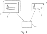
- an input image 1 captured by a sensor 3 might display unwanted distortion caused by a lens.
- data of the input image 1 are processed by an image processing device 9.
- Bird View Another example of such a visual effect is called "Bird View”.
- the image displayed to the driver looks as if it were taken from above the vehicle with the camera facing downwards.
- desired visual effect is achieved by repositioning the pixels of the image obtained from the sensor (input image) thus forming output image, which is displayed to the driver.
- WO 2006/128862 A1 discloses an integrated circuit for the electronic manipulation of images, a method for the electronic manipulation of images by means of warping, a system for the electronic manipulation of images comprising an integrated circuit, and also a use of the integrated circuit.
- the integrated circuit has a main processor unit, a memory access control unit, a graphics output control unit and a warping calculation unit.
- US 5 204 944 relates to a two-dimensional image subjected to a three-dimensional effect, such as folding, twisting or rotation, and transformed or warped into a modified output image.
- a three-dimensional effect such as folding, twisting or rotation
- transformed or warped into a modified output image By successive one-dimensional resampling along two coordinates and parallel channel processing of transposed input image data with rejection of distorted pixel value data, bottleneck, shear and other distortions are addressed.
- Complete warping systems, resampling subsystems and related methods are disclosed.
- US 5 208 872 discloses an apparatus for image processing comprising a camera for receiving an original visual image and transforming the original visual image into an analog image, a first converter for transforming the analog image of the camera to a digital image, a processor having a single flow architecture for receiving the digital image and producing, with a single algorithm, an output image, a second converter for transforming the digital image of the processor to an analog image, and a viewer for receiving the analog image, transforming the analog image into a transformed visual image for observing the transformations applied to the original visual image.
- the processor comprises one or more sub-processors for the parallel reception of a digital image for producing an output matrix of the transformed visual image.
- the processor comprises a plurality of sub-processors for receiving in parallel and transforming the digital image for producing a matrix of the transformed visual image, and an output interface means for receiving the respective portions of the transformed visual image from the respective sub-processor for producing an output matrix of the transformed visual image.
- one output image pixel 11 is mapped between the four pixels 13 of the input image.
- at least one characteristic value of the output image pixel 11 is calculated by interpolating corresponding characteristic values of the surrounding input image pixels 13.
- the video stream consisting of the sequence of images must be processed in real time, i.e. the processing time for one image (frame) must not exceed the time between the two consequent frames output by the sensor.
- the processing time for one image must not exceed the time between the two consequent frames output by the sensor.
- the maximum time allowed for processing of a single frame is 33.3 ms.
- An image processing device 14 capable of doing said processing might have a general setup as shown schematically in Fig. 3 , that comprises at least an image processing unit 15, internal RAM (random-access memory) device 19, external RAM device 17, and ROM (read-only memory, nonvolatile memory) device 21.
- internal RAM random-access memory
- ROM read-only memory, nonvolatile memory
- the ROM device 21 contains the program code executed by the image processing unit 15, as well as some data required to perform said processing. The content of the ROM device 21 does not change during normal operation of the image processing device 14.
- External RAM device 17 contains at least two buffers: one to store input image data (input buffer), and another to store output image data (output buffer). Both input and output buffers are arranged in a pixel order, i.e. in such a way, that adjacent pixels in the same row of the image occupy adjacent cells of the buffer, and the last pixel of one image row is immediately followed by the first pixel of the next image row.
- the memory is addressed in a "cell by following cell” order, i.e. a first cell is read followed by a an adjacent, neighboring second cell, followed by a third cell adjacent to the second cell opposite the first cell and so on.
- the image processing unit 15 remaps the pixels of the input image contained in the input buffer to the pixels of the output image in the output buffer in such a way that the desired visual effect is achieved; in particular a distortion caused by a lens is reduced or eliminated.
- the image processing unit 15 can be implemented for example as a digital signal processor (DSP), a field programmable gate array (FPGA), or an application specific integrated circuit (ASIC).
- DSP digital signal processor
- FPGA field programmable gate array
- ASIC application specific integrated circuit
- the external RAM device 17 represents an external storage device and internal RAM device 19 represents an internal storage device.
- the external RAM device 17 for example DDR2 SDRAM (double data rate synchronous dynamic random-access memory), might be implemented as a separate integrated circuit, i.e. might be physically separated from the image processing unit 15.
- the external RAM device 17 has sufficient capacity to accommodate the input and output buffers.
- read operations 23 and write operations 25 between external RAM device 19 and image processing unit 15 cause stalls of the latter, because external RAM device 17 is typically clocked at significantly lower frequency.
- An internal RAM device 19 might be implemented on the same integrated circuit as the image processing unit 15. Therefore, internal RAM device 19 operates at the same clock frequency as the image processing unit 15. This allows performing read operations 27/ write operations 29 sufficiently fast to avoid stalls of the image processing unit 15, or at least, reduce their duration in comparison to external RAM device 17.
- internal RAM device 19 can be used as an addressable cache, and in this case, it is managed by a cache controller.
- the main idea behind the cache is that whenever some address, i.e. a respective memory cell is accessed by a read operation 31 in the external RAM device 17, an entire block of data containing the desired memory cell is fetched into internal RAM device 19. If the same address/cell or any other address/cell in the same block is accessed again, data in the internal RAM device 19 is reused, thus avoiding access to the external RAM device 17.
- This technique minimizes stalls of the image processing unit 15, if assumption about temporal and spatial locality of the data holds, which is often the case in the image processing.
- write operations to the external RAM device 17 can be carried out such that not only a single cell but a complete block is transferred from the internal RAM device 19 to the external RAM device 17 by a write operation 33.
- external memory RAM blocks can be configured as cacheable or non-cacheable.
- the output buffer is placed in the non-cacheable external RAM.
- the input buffer is located in the cacheable external RAM, because each element of the input buffer is likely to be accessed multiple times, as the same value can be involved into interpolation at several locations. In this case, cache can boost the system performance by reusing the data in the internal memory and thus avoiding processor stalls associated with the external memory access.
- a mapping function required to achieve a targeted visual effect i.e. correspondence between the locations of input and output image, is used and usually represented in the form of a lookup table (LUT).
- LUT contains one entry per pixel of the output image. Every entry n of the LUT preferably contains the following fields:
- the LUT can be calculated before the image processing starts and stored in the non-cacheable external RAM, or alternatively, might be pre-calculated externally with respect to the image processing device and stored in the ROM.
- the following method can be employed to calculate LUT:
- This known method has however the drawback that accessing the input image data stored in the input memory device leads to stalls of the imaging processing unit although the internal RAM is used as a cache.
- This objective is achieved by arranging the entries within the lookup table in such a way that when processing the lookup table the input memory device is addressed in a sequential reading order.
- the processing of the lookup table means, especially that the table is read "entry by entry” to reach the remapping of the input picture data into the output picture data.
- At least two pixels of the input image, preferably a plurality of pixels, of the input image are read and processed to calculate one single output image pixel.
- a sequential reading order means especially that the input memory device is addressed such that a cell located before a following or subsequent cell in the memory is read timely before the subsequent cell, especially that it is addressed cell by adjacent cell.
- the addressing might include also skipping single or plurality cells or that at least all cells within a specified cell group or cell block necessary for the remapping are addressed (however not necessarily cell by cell within the group) before a cell in an adjacent cell group is addressed.
- the cell group might be formed by the cells loadable into the internal storage device and/or cache as explained in the following.
- the entries within the lookup table might be arranged in such a way that the input image data in the external RAM are addressed in a pixel order.
- An inventive method might be characterized in that the entries within the lookup table are arranged before the transfer of the input image data into the output image data and/or in that as desired visual effect a correction of lens distortion effect and/or the generating of a bird view is/are achieved.
- the invention furthermore proposes that the input memory device comprises at least one input buffer, especially for storing the input image data, and/or the output memory comprises at least one output buffer for storing the output image data.
- the lookup table is generated as a list, having a plurality of entries, each comprising for a respective pixel at least one position value, a least one input memory address field (LUT[n].InAddr) representing a memory address in the input memory device and/or the input buffer, at least one horizontal interpolation coefficient (LUT[n].Ch) and at least one vertical interpolation coefficient (LUT[n].Cv), is provided.
- LUT[n].InAddr representing a memory address in the input memory device and/or the input buffer
- LUT[n].Ch horizontal interpolation coefficient
- LUT[n].Cv vertical interpolation coefficient
- the position value is calculated based on a row position and a column position of the pixel in the input image, especially by adding to the column position the product of the row position multiplied with the number of columns of the input image, and/or a respective value of the input memory address field (LUT[n].InAddr), the horizontal interpolation coefficient (LUT[n].Ch) and the vertical interpolation coefficient (LUT[n].Cv) is calculated based on the data remapping function, preferably describing a transformation of pixel coordinates (x, y) required to perform the visual effect.
- At least one transformation value is calculated based on the data remapping function, especially at least one first transformation value based on a first data remapping function and at least one second transformation value based on a second data remapping function, wherein preferably the respective value of the input memory address field (LUT[n].InAddr) is calculated by adding to the floor value of the first transformation value (floor(xi)) the product of the floor value of the second transformation value (floor(yi)) multiplied with the number of columns (width) of the input image, the horizontal interpolation coefficient (LUT[n].Ch) is calculated by subtracting from the first transformation value (xi) the floor value of the first transformation value, and/or the vertical interpolation coefficient (LUT[n].Cv) is calculated by subtracting from the second transformation value the floor value of the second transformation value(floor(yi)).
- An inventive method might be furthermore characterized in that after generating the lookup table and/or before the transfer of the input image data into the output image data the entries within the lookup table are rearranged based on a sort function, wherein the sort function preferably comprises at least one bubble sort function, at least one quick sort function, at least one merge sort function, at least one insertion sort function, at least one tree sort function, at least one comb sort function, at least one gnome sort function, at least one heap sort function, at least one intro sort function, at least one selection sort function, at least one shaker sort function, at least one shell sort function, at least one smooth sort function, at least one stooge sort function, at least one swap sort function, at least one bucket sort function, at least one counting sort function and/or at least one radix sort function.
- the sort function preferably comprises at least one bubble sort function, at least one quick sort function, at least one merge sort function, at least one insertion sort function, at least one tree sort function, at least one comb sort function, at least
- the invention might be furthermore characterized in that the input image data are stored in the input memory device and/or the output image data are stored in the output memory device in a pixel order, especially data of adjacent pixels in a row of the input image are stored in adjacent cells of the input memory device and data of a pixel at an end of a row of the input image are stored in a cell of the input memory device followed by a cell in which the data of a pixel of a following row of the input image are stored and/or data of adjacent pixels in a row of the output image are stored in adjacent cells of the output memory device and data of a pixel at an end of a row of the output image are stored in a cell of the output memory device followed by a cell in which the data of a pixel of a following row of the output image are stored.
- the entries in the lookup table are processed in a sequential processing, especially reading, order and when following this sequential processing order the input memory device, especially the cells of the input memory device, is/are addressed in a sequential reading order.
- an inventive method might be characterized in that the transfer of the data comprises reading a first entry in the lookup table comprising information on the pixel to be read out of the input memory device, especially a first memory address in the input memory device, preferably the input memory address field (LUT[n].InAddr), and a second memory address in the output memory device, wherein especially the position value is used as an output memory address field (LUT[n].OutAddr), at least indirectly addressing a respective cell, especially identified by the first input memory, address in the input memory device, reading the input image data stored in said cell of the input memory device, addressing a respective cell, especially identified by the second memory address, in the output memory device and storing said read input image data based on the data stored in the lookup table in said cell in the output memory device.
- the input buffer and/or the output buffer are at least partly located within an external storage device, especially comprising a random-access memory and/or preferably located externally to and/or physically separated from an image processing unit, and/or when reading data out of a respective cell of the input buffer and/or the output buffer of the external storage device the data is copied into and/or cached in an internal storage device, especially in an input buffer and/or output buffer of the internal storage device, wherein the internal storage device preferably comprises a random-access memory and/or is located internally of the image processing unit, wherein especially data stored in neighboring cells of the respective cells are also copied into/cached as a block in the internal storage device.
- read/write operations of the image processing unit are performed faster with the internal storage device than with the external storage device, especially stalls of the image processing unit is avoided or reduced when read/write operations of the image processing unit are performed with the internal storage device.
- the internal storage device is accessed to read the input image data for the transfer and in case the required data are not available/are not cached in the internal storage device, the external storage device, especially the input buffer, is accessed to read the data for the transfer.
- the lookup table is generated by the image processing unit or is generated by a processing unit being separated from the image processing unit and/or the lookup table is stored within a read-only memory connected to the image processing unit, especially also storing program code information executed by the image processing unit for processing the input image data.
- the data remapping function comprises a bilinear interpolation.
- the invention furthermore provides a computer readable medium having stored thereon program code to carry out an inventive method.
- the invention provides a device image processing, comprising at least one image processing unit, at least one input memory device in which data of at least one input image are storable and at least one output memory device in which data of at least one output image are storable, wherein the image processing unit is configured to carry out an inventive method.
- the device comprises at least one image sensor, wherein the data provided by the image sensor are input into and/or stored in the input memory device.
- the claimed invention is based on the surprising finding that by a simple re-ordering of the data stored in the lookup table for an image transformation a fast real time imaging processing can be achieved. It was recognized by the inventors that the nature of wanted visual effects, for example lens distortion, makes pixels of the input image to be accessed in an order different from the pixel order in the image and thus different from the order of the data fields in the input memory device / input buffer. Due to the manufacturing constraints, power consumption and cost considerations, an internal RAM of an image processing device has usually the volume sufficient to accommodate only a few image rows.
- typical up to date DSP features 128 kilobytes of internal RAM 19, which is just enough to store about 25 rows of an input image, assuming typical IMPix sensor (1280 x 800 pix) is used.
- typical IMPix sensor (1280 x 800 pix) is used.
- the processing speed can be increased by avoiding the need to access an external storage device instead of using data that is already stored within an internal storage device / cache.
- the lookup table is adapted to the data that are accessible within the internal storage device / cache.
- a position value always existing within an image processing lookup table as an identifier for an output memory address allows a reordering of the entries in the lookup table without negatively influencing the ability to address the correct location within the output image memory device.
- the claimed invention is thus based on the finding that the transformation of the input image data has to be aligned with the order of image data as stored in the input memory device in comparison to the method used in the state of the art where the imaging data processing is aligned with the order of the data stored in the output memory device in which the output image data are stored.
- the entries of the lookup table are rearranged in such a way, that during the transformation process the input image data is accessed in a row order, i.e. in the same order, as the image rows are output by the sensor.
- the image data in the input memory device are addressed cell by following cell or at least, cell group by following cell group. Doing this, allows each line of the input image to be loaded into the cache only once, thus minimizing the number of accesses of external storage device and minimizing associated image processing unit stalls.
- Figure 4 it is visualized how in an imaging processing method according to the state of the art the input image data, that are stored in an input buffer 51, are accessed to transform the image data via a lookup table 53 into an output image stored in an output buffer 55.
- the input buffer 51 comprises a plurality of cells 57, 59, 61, 63, 65, 67, 69.
- the input image data are stored in a pixel order.
- the input image has a width defined by the number of columns in the input image and a height defined by the number of rows in the input image.
- the data concerning the input image data of the first row are stored in the input buffer 51 such that the data of each pixel are stored in a cell (for example cell 57) followed by a cell (for example cell 59) in which the data of the pixel in the next column of the same row are stored and that a cell in which the data of the last pixel of one row are stored (for example cell 63) are followed by a cell (for example cell 65) in which the data of the pixels of a following row of the image are stored.
- the data stored in the input buffer are not accessed in the order how they are stored in the input buffer 51.
- the output image stored in the output buffer 55 it is generated column by column in each row of the output image and row by row it is necessary to access data stored in different places within the input buffer 51 to calculate the respective data for the output image pixel. For example to calculate the data for an image pixel stored in cell 71 of the output buffer 55 the cells 63, 65, 67 and 69 have to be accessed.
- the input buffer is cacheable when reading cell 63 out of the input buffer of the external storage device/external RAM all data stored in block 73 are transferred into the internal RAM/cache, especially the input buffer of the internal storage device/internal RAM. This allows to read cell 65 out of the cache without the need to re-access the (slower) external RAM.
- cell 67 is not comprised by block 73 and thus is not read into the cache when reading cells 63, 65.
- external RAM has to be accessed and block 75 is transferred into the cache and block 73 is overwritten within the cache. This leads to a significant delay in the processing.
- cell 69 has to be accessed and cell 69 is not comprised by block 75 again the external RAM has to be accessed instead of internal RAM / cache.
- pixels that are in the same row of the output image are mapped through the lookup table 53 on the pixels of the input image that are located in the different rows, that means not in a sequential order within the input buffer 51.
- a first cell being located before a second cell in the input buffer is read / addressed timely after the second cell.
- a lookup table 83 ( Fig. 6 ) includes a plurality of entries, each entry containing at least the following fields:
- the lookup table (83) entries are rearranged in a way that for every entry n from 0 to N-2 holds the equation: LUT n . InAddr ⁇ LUT n + 1 . In Addr .
- every next entry of the lookup table 83 refers to the higher or the same address in the input buffer 81 as the previous.
- the input buffer 81 is accessed in the pixel order cell order and every row is loaded into the internal storage device / cache no more than once during frame processing.
- a flow diagram of the inventive method usable with an image processing device as shown in figure 3 and described above is given.
- a remapping function to reach a wanted visual effect is defined.
- a lookup table 83 (see figure 6 ) is calculated.
- the entries within the lookup table 83 are rearranged in the before described manner and in step 106 the lookup table 83 is stored.
- the lookup table 83 can be calculated and rearranged by the image processing device or image processing unit itself or might be build and rearranged externally with respect to the imaging processing device.
- the lookup table 83 might be generated on an external computer and the resulting lookup table 83 is stored in the ROM of the imaging processing device. For example it might be loaded during a boot-up phase of the imaging processing device and might be used during the imaging processing by the imaging processing unit.
- An image processing is described in figure 5 in steps 108 to 122.
- the input image is captured.
- the input image data provided by the sensor / camera are stored in the input buffer 81.
- the image processing unit uses the lookup table 83 to transfer the input image data into the output image data.
- the entries of the LUT are addressed one of another, ie. sequentially, and due to the rearrangement of the LUT the input buffer is accessed and this leads to the result that a part of the image data in form of a block of a plurality of cells are read out of the input buffer of the external storage device (step 112) and is written to the internal storage device / cache in step 114.
- the image processing unit accesses the internal storage device in the steps 116 to 120.
- Step 112 i.e. accessing the input buffer of external storage device, is only carried out in case it is decided in step 122 that the processing of the complete image data is finalized, or in case in step 118 it is analyzed that the end of the block, stored in the cache, is reached, and the following block has to be read out from the external storage device.
- step 122 it is decided, whether the complete input image is processed. If this is not the case, the method returns to step 116, and the next output image pixel is calculated/remapped. In case in step 122 it is decided that the input image has been processed completely, the method returns to step 108 and awaits that another input image it captured.
- FIG. 6 The general concept of accessing the input buffer / cache when using the inventive method is shown in figure 6 .
- the accessing for four output image pixels is shown.
- the data stored in the input buffer 81 that are a least partly stored in the internal storage device / cache are accessed in the order of their storage in the respective memory.
- the output buffer 85 is accessed to store the respective pixel.
- the output buffer is, however, not accessed in a sequential order.
- the cells 87a to 87d sequentially ordered in the input buffer 81, are accessed to remap the data stored therein and to store the remapped data in cell 89 of the output buffer 85.
- the following cells 91a to 91d forming a cell group or cell block in the input buffer 81 are accessed to remap data to generate the data to be stored in cell 93 of the output buffer.
- the same is applied to the following cells 95a to 95d, in order to generate the data of the output image to be stored in cell 97 of the output buffer.
- the method proceeds then by reading data stored in cells 98a to 98d that are directly following cell 95d in the input buffer 81 and storing remapped data in cell 99 of the output buffer 85.
- each data cell within the output buffer 85 is only accessed one time during the calculation of the respective output image pixel.
- the input buffer 81 is accessed a plurality of times, so that any time delay in accessing the input buffer / cache 81 leads to a more significant time delay when compared to accessing the not cached output buffer. Due to the reduced reading time in the internal storage device / input buffer / cache the inventive results might also be achieved by addressing cell groups / cell blocks sequentially to each other.
- the cell group might be formed by the cells of the external RAM stored in the input buffer / cache whereas cells of following cell groups are cells in the external RAM loaded subsequently into the input buffer / cache.
- the input buffer 81 is accessed for example four times more often than the output buffer 85, the overall number processor stalls is significantly reduced.
- the entries of lookup table can be rearranged by a plurality of algorithms.
- a plurality of algorithms For example an algorithm referred to as “Bubble Sort Algorithm” might be used:
- the lookup table 83 is rearranged before the actual image processing starts.
- the lookup table 83 can be built and rearranged externally with respect to the image processing device 14, for example on a separate computer.
- the pixels of the input buffer might be repositioned/remapped by using the following algorithm.
- figure 7 it is shown how a distorted pixel Q can be transferred into an undistorted pixel P by interpolating characteristic values of pixels A-D neighboring the distorted pixel Q.
- pixels A to D and P lay on a regular structure (image or monitor pixels). Then, pixel P can be regarded as an undistorted pixel, where pixel Q is its distorted counterpart. Furthermore, pixel P is always located on a regular structure, while pixel Q is in general not part of the raster.
- an undistorted line 151 of an output image can be reproduced from a distorted line 153, which itself is composed of several image-lines 155 in an input image.
- V Q dx ⁇ dy ⁇ V D ⁇ dx ⁇ dy ⁇ V C ⁇ dx ⁇ dy ⁇ V B + dx ⁇ dy ⁇ V A + dx ⁇ V B ⁇ dx ⁇ V A + dy ⁇ V C ⁇ dy ⁇ V A + V A
- V Q V A ⁇ 1 ⁇ dy ⁇ dx + dx ⁇ d + V B + dx ⁇ dx ⁇ dy + V C ⁇ dy ⁇ dx ⁇ dy + V D dx ⁇ dy
- V Q V A ⁇ 1 + dx ⁇ dy ⁇ dx ⁇ dy + V B ⁇ dx ⁇ dx ⁇ dy ) + V C ⁇ dy ⁇ dx ⁇
- the contribution of the point Q can be calculated by using the appropriate summand.
- the claimed method and device allows a real time image transformation, such as distortion correction or "Bird View".
- the transformation relies on a lookup table rearranged in such a way, that the elements of an input buffer are accessed in a pixel order. This provides inter alias an advantage by reducing processing time when using cache for temporal storage of a part of the input image.
- the claimed method and device allows a real time image transformation, such as distortion correction or "Bird View".
- the transformation relies on a lookup table rearranged in such a way, that the elements of an input buffer are accessed in a pixel order. This provides inter alias an advantage by reducing processing time when using cache for temporal storage of a part of the input image.
Landscapes
- Engineering & Computer Science (AREA)
- Physics & Mathematics (AREA)
- General Physics & Mathematics (AREA)
- Theoretical Computer Science (AREA)
- Multimedia (AREA)
- Signal Processing (AREA)
- Image Processing (AREA)
Claims (16)
- Verfahren zum Verarbeiten von Eingangsbilddaten (1) durch eine Bildverarbeitungsvorrichtung (14), um einen gewünschten visuellen Effekt in einem Ausgangsbild (5) zu erreichen, wobei die Eingabebilddaten in einer Eingabespeichervorrichtung gespeichert sind, die mindestens einen Eingabepuffer (81) umfasst und mindestens teilweise in einer externen Speichervorrichtung (17) angeordnet sind, die extern zu einer Bildverarbeitungseinheit (15) der Bildverarbeitungsvorrichtung (14) und/oder physisch von dieser getrennt ist, und die Eingabebilddaten (1) basierend auf Daten einer Umsetzungstabelle (83) in entsprechende Ausgabebilddaten (5) übertragen werden, die in einer Ausgabespeichervorrichtung mit einem Ausgabepuffer (85) gespeichert sind, wobei beim Auslesen von Daten aus einer entsprechenden Zelle, die die Bilddaten eines Bildpunkts des Eingangspuffers (81) umfasst, ein Teil der Eingangsbilddaten in Form einer Gruppe von Zellen in eine interne Speichervorrichtung (19) kopiert und/oder zwischengespeichert wird, wobei Lese-/Schreiboperationen (23, 25, 27, 29) der Bildverarbeitungseinheit (15) mit der internen Speichervorrichtung (19) schneller durchgeführt werden als mit der externen Speichervorrichtung (17), wobei die Umsetzungstabelle (83) basierend auf mindestens einer Datenneuzuordnungsfunktion (f1, f2) erzeugt wird, die erforderlich ist, um den gewünschten visuellen Effekt zu erzielen, dadurch gekennzeichnet, dass die Einträge innerhalb der Umsetzungstabelle (83) so angeordnet sind, dass beim Verarbeiten der Umsetzungstabelle (83) durch eintragsweises Lesen der Tabelle die Eingabespeichervorrichtung (81) in einer sequentiellen Lesereihenfolge angesprochen wird, so dass die Einträge der Umsetzungstabelle in einer auf- oder absteigenden Reihenfolge eines Eingabespeicheradreßfeldes (LUT[n].Addr) sortiert werden zum Identifizieren einer Speicheradresse im Eingangspuffer (81), wodurch auf die Eingangsbilddaten in der Reihenfolge zugegriffen wird, in der sie im Eingangspuffer und damit in der internen Speichervorrichtung (19) gespeichert sind, ohne auf den Eingangspuffer (81) der externen Speichervorrichtung zum Empfangen von Eingangsbilddaten zuzugreifen, bis alle Daten im Cache verwendet wurden, wobei der Ausgangspuffer
(85) in einer nicht sequentiellen Reihenfolge zugegriffen wird, solange keine Zelle innerhalb einer anderen Zellgruppe adressiert wird, wobei jede Datenzelle innerhalb des Ausgabepuffers (85) nur einmal während der Berechnung eines jeweiligen Ausgabebild Bildpunkts (93, 99) zugegriffen wird und wobei die Zellgruppe durch die in den Eingabepuffer (81) und damit in den internen Speicher geladenen Zellen gebildet wird Speichervorrichtung (19), wobei Zellen der folgenden Gruppen Zellen sind, die anschließend in den Eingangspuffer (81) und damit in die interne Speichervorrichtung (19) geladen werden. - Verfahren nach Anspruch 1, dadurch gekennzeichnet, dass
die Einträge innerhalb der Umsetzungstabelle (83) vor der Übertragung der Eingangsbilddaten in die Ausgangsbilddaten angeordnet sind, und/oder dadurch gekennzeichnet, dass
als gewünschter visueller Effekt eine Korrektur des Linsenverzerrungseffekts und/oder die Erzeugung einer Vogelperspektive erreicht wird. - Verfahren nach einem der vorstehenden Ansprüche, dadurch gekennzeichnet, dass
der Ausgabespeicher mindestens einen Ausgabepuffer (85) zum Speichern der Ausgabebilddaten umfasst. - Verfahren nach einem der vorstehenden Ansprüche, dadurch gekennzeichnet, dass Umsetzungstabelle (83) als Liste mit einer Vielzahl von Einträgen erzeugt wird, die jeweils für ein Bildpunkt mindestens einen Positionswert (n) das Eingabespeicheradressfeld (LUT[n]. InAddr), das eine Speicheradresse in der Eingabespeichervorrichtung und/oder dem Eingabepuffer (81) darstellt, mindestens einen horizontalen Interpolationskoeffizienten (LUT[n].Ch) und mindestens einen vertikalen Interpolationskoeffizienten (LUT[n]..Cv) vorsieht, umfasst, wobei vorzugsweise zum Erzeugen der Umsetzungstabelle (83) für jeden Bildpunkt des Eingabebildes (1) der Positionswert (n) basierend auf einer Zeilenposition (y) und einer Spaltenposition (x) des Bildpunkts im Eingabebild berechnet wird, insbesondere durch Addieren des Produkts der Zeilenposition (y) multipliziert mit der Anzahl der Spalten des Eingabebildes zu der Spaltenposition (x) und/oder wobei vorzugsweise ein entsprechender Wert des Eingabespeicheradressfeldes (LUT[n]. InAddr), der horizontale Interpolationskoeffizient (LUT[n]. Ch) und der vertikale Interpolationskoeffizient (LUT[n]. Cv) basierend auf der Datenneuzuordnungsfunktion (f1, f2) berechnet wird, vorzugsweise eine Transformation von Bildpunktkoordinaten (x,y) beschreibend, die zur Durchführung des visuellen Effekts erforderlich ist.
- Verfahren nach Anspruch 4, dadurch gekennzeichnet, dass
zum Erzeugen der Umsetzungstabelle (83) für jeden Bildpunkt des Eingabebildes (1) mindestens ein Transformationswert (xi, yi) basierend auf der Datenneuzuordnungsfunktion (f1, f2) berechnet wird, vorzugsweise mindestens ein erster Transformationswert (xi) basierend auf einer ersten Datenneuzuordnungsfunktion (f1) und mindestens ein zweiter Transformationswert (yi) basierend auf einer zweiten Datenneuzuordnungsfunktion (f2), wobei vorzugsweise der jeweilige Wert des Eingabespeicheradressfeldes (LUT[n])InAddr) berechnet wird, indem zur Wertuntergrenze des ersten Transformationswertes (floor(xi)) das Produkt aus die Wertuntergrenze des zweiten Transformationswertes (floor(yi)) multipliziert mit der Anzahl der Spalten (Breite) des Eingangsbildes (1) addiert wird, der horizontalen Interpolationskoeffizienten (LUT[n].Ch) berechnet wird, indem vom ersten Transformationswert (xi) die Wertuntergrenze des ersten Transformationswertes subtrahiert wird, und/oder der vertikale Interpolationskoeffizient (LUT[n]. Cv) berechnet wird, indem vom zweiten Transformationswert die Wertuntergrenze (yi) des zweiten Transformationswertes (floor(yi)) subtrahiert wird. - Verfahren nach einem der vorstehenden Ansprüche, dadurch gekennzeichnet, dass
nach dem Erzeugen der Umsetzungstabelle (83) und/oder vor der Übertragung der Eingangsbilddaten in die Ausgangsbilddaten die Einträge innerhalb der Umsetzungstabelle (83) basierend auf einer Sortierfunktion neu angeordnet werden, wobei das Verfahren insbesondere dadurch gekennzeichnet ist, dass
die Sortierfunktion umfasst mindestens eine Bubblesort-Funktion, mindestens eine Schnellsortierfunktion, mindestens eine MergesortFunktion, mindestens eine Insertionsort-Funktion, mindestens eine Treesort-Funktion, mindestens eine Combsort-Funktion, mindestens eine Gnomensort-Funktion, mindestens eine HeapsortFunktion, mindestens eine Introsort-Funktion, mindestens eine Selectionsort-Funktion, mindestens eine Shakersort-Funktion, mindestens eine Shellsort-Funktion, mindestens eine Smoothsort-Funktion, mindestens eine Stoogesort-Funktion, mindestens eine Swapsort-Funktion-Sortierfunktion, mindestens eine Bucketsort-Funktion-Sortierfunktion, mindestens eine Countingsort-Funktion und/oder mindestens eine Radixsort-Funktion. - Verfahren nach einem der vorstehenden Ansprüche, dadurch gekennzeichnet, dass
die Eingangsbilddaten in der Eingangsspeichervorrichtung (51, 81) gespeichert sind und/oder die Ausgangsbilddaten in der Ausgangsspeichervorrichtung (55, 85) in einer Bildpunktreihenfolge gespeichert sind, wobei insbesondere Daten benachbarter Bildpunkte in einer Reihe des Eingangsbildes (1) in benachbarten Zellen (59, 61) der Eingabespeichervorrichtung (51, 81) und Daten eines Bildpunkts an einem Ende einer Zeile des Eingabebildes (1) in einer Zelle (63) der Eingabespeichervorrichtung (81) gespeichert sind, gefolgt von einer Zelle (65), in der die Daten eines Bildpunkts einer nachfolgenden Zeile des Eingabebildes (1) gespeichert sind und/oder wobei insbesondere Daten benachbarter Pixel in einer Zeile der Ausgabebild (5) in benachbarten Zellen der Ausgabespeichervorrichtung (85) gespeichert sind und Daten eines Bildpunkts am Ende einer Zeile des Ausgabebildes (5) in einer Zelle der Ausgabespeichervorrichtung (85) gespeichert sind, gefolgt von einer Zelle, in der die Daten eines Bildpunkteiner nachfolgenden Zeile des Ausgabebildes (5) gespeichert sind. - Verfahren nach einem der vorstehenden Ansprüche, dadurch gekennzeichnet, dass
für die Übertragung der Daten die Einträge in der Umsetzungstabelle (83) in einer sequentiellen Verarbeitungsreihenfolge verarbeitet werden und die Eingabespeichervorrichtung, wenn sie dieser sequentiellen Reihenfolge folgt, in einer sequentiellen Lesereihenfolge adressiert wird, wobei vorzugsweise die Zellen der Eingabespeichervorrichtung (87a - 98d) in einer sequentiellen Lesereihenfolge adressiert werden. - Verfahren nach einem der vorstehenden Ansprüche, dadurch gekennzeichnet, dass
die Übertragung der Daten das Lesen eines ersten Eintrags in der Umsetzungstabelle (83) umfasst, der Informationen über das aus der Eingabespeichervorrichtung auszulesende Bildpunkte umfasst, insbesondere eine erste Speicheradresse in der Eingabespeichervorrichtung (81), vorzugsweise das Eingabespeicheradressfeld (LUT[n]. InAddr), und eine zweite Speicheradresse in der Ausgabespeichervorrichtung (85), worin insbesondere der Positionswert (n) als Ausgabespeicheradressfeld (LUT[n] OutAddr), verwendet wird, mindestens indirektes Adressieren einer jeweiligen Zelle (87a - 98d), insbesondere durch den ersten Eingabespeicher identifiziert Adresse in der Eingabespeichervorrichtung (81), Lesen der in der Zelle (87a - 98d) der Eingabespeichervorrichtung (81) gespeicherten Eingabebilddaten, Adressieren einer jeweiligen Zelle (89, 93, 97, 99), insbesondere durch die zweite Speicheradresse identifiziert, in der Ausgabespeichervorrichtung (85) und Speichern der gelesenen Eingabebilddaten basierend auf den in der Umsetzungstabelle gespeicherten Daten. (83) in der Zelle (89, 93, 97, 99) in der Ausgabespeichervorrichtung (85). - Verfahren nach einem der vorstehenden Ansprüche, dadurch gekennzeichnet, dass der Ausgangspuffer (83) zumindest teilweise innerhalb der externen Speichervorrichtung (17) angeordnet ist, und/oder die externe Speichervorrichtung (17) einen Direktzugriffsspeicher umfasst und/oder dadurch gekennzeichnet, dass
beim Auslesen von Daten aus einer entsprechenden Zelle des Ausgabepuffers (85) der externen Speichervorrichtung die Daten in die interne Speichervorrichtung (19) kopiert und/oder zwischengespeichert werden, wobei aus dem Eingabepuffer und/oder der Ausgabepuffer der externen Speichervorrichtung ausgelesene Daten in einen Eingabepuffer und/oder Ausgabepuffer der internen Vorrichtung kopiert und/oder zwischengespeichert werden, und/oder die interne Speichervorrichtung einen Direktzugriffsspeicher umfasst und/oder sich innerhalb der Bildverarbeitungseinheit (15) befindet, wobei vorzugsweise in benachbarten Zellen der jeweiligen Zellen gespeicherte Daten auch als Block in der internen Speichervorrichtung (19) kopiert/cached werden. - Verfahren nach einem der vorgehenden Ansprüche, dadurch gekennzeichnet, dass
ein Blockieren der Bildverarbeitungseinheit (15) vermieden oder reduziert wird, wenn Lese-/Schreiboperationen (27, 29) der Bildverarbeitungseinheit (15) mit der internen Speichervorrichtung (19) durchgeführt werden. - Verfahren nach Anspruch 10 oder 11, dadurch gekennzeichnet, dass
zuerst auf die interne Speichervorrichtung (19) zugegriffen wird, um die Eingangsbilddaten für die Übertragung zu lesen, und falls die erforderlichen Daten nicht verfügbar sind oder nicht in der internen Speichervorrichtung (19) zwischengespeichert werden, auf die externe Speichervorrichtung, insbesondere den Eingangspuffer (19), zugegriffen wird, um die Daten für die Übertragung zu lesen. - Verfahren nach einem der vorstehenden Ansprüche, dadurch gekennzeichnet, dass
die Umsetzungstabelle (83) von der Bildverarbeitungseinheit (15) erzeugt wird oder von einer Verarbeitungseinheit erzeugt wird, die von der Bildverarbeitungseinheit (15) getrennt ist, dadurch gekennzeichnet, dass
die Umsetzungstabelle (83) in einem mit der Bildverarbeitungseinheit (15) verbundenen schreibgeschützten Speicher (21) gespeichert ist, insbesondere auch Programmcodeinformationen, die von der Bildverarbeitungseinheit (15) zur Verarbeitung der eingegebenen Bilddaten ausgeführt werden und/oder dadurch gekennzeichnet, dass die Datenneuzuordnungsfunktion eine bilineare Interpolation umfasst. - Computerlesbares Medium mit darauf gespeichertem Programmcode zur Durchführung eines Verfahrens nach einem der vorhergehenden Ansprüche.
- Bildverarbeitungsvorrichtung zur Durchführung des Verfahrens nach einem der vorstehenden Ansprüche, umfassend mindestens eine Bildverarbeitungseinheit (15), mindestens eine Eingabespeichervorrichtung (81), in der Daten mindestens eines Eingangsbildes speicherbar sind, und mindestens eine Ausgabespeichervorrichtung (85), in der Daten mindestens eines Ausgangsbildes speicherbar sind, wobei die Bildverarbeitungseinheit (15) konfiguriert ist, ein Verfahren nach einem der Ansprüche 1 bis 13 durchzuführen.
- Bildverarbeitungsvorrichtung nach Anspruch 15, dadurch gekennzeichnet, dass
die Vorrichtung mindestens einen Bildsensor (3) umfasst, wobei die vom Bildsensor (3) bereitgestellten Daten in die Eingangsspeichervorrichtung (81) eingegeben und/oder gespeichert werden.
Priority Applications (1)
| Application Number | Priority Date | Filing Date | Title |
|---|---|---|---|
| EP14724714.2A EP2997539B1 (de) | 2013-05-16 | 2014-05-13 | Verfahren und vorrichtung zur verarbeitung von eingabebilddaten |
Applications Claiming Priority (3)
| Application Number | Priority Date | Filing Date | Title |
|---|---|---|---|
| EP13168085.2A EP2804144A1 (de) | 2013-05-16 | 2013-05-16 | Verfahren und Vorrichtung zur Verarbeitung von Eingabebilddaten |
| PCT/EP2014/059788 WO2014184202A1 (en) | 2013-05-16 | 2014-05-13 | Method and device for processing input image data |
| EP14724714.2A EP2997539B1 (de) | 2013-05-16 | 2014-05-13 | Verfahren und vorrichtung zur verarbeitung von eingabebilddaten |
Publications (2)
| Publication Number | Publication Date |
|---|---|
| EP2997539A1 EP2997539A1 (de) | 2016-03-23 |
| EP2997539B1 true EP2997539B1 (de) | 2019-12-11 |
Family
ID=48577490
Family Applications (2)
| Application Number | Title | Priority Date | Filing Date |
|---|---|---|---|
| EP13168085.2A Withdrawn EP2804144A1 (de) | 2013-05-16 | 2013-05-16 | Verfahren und Vorrichtung zur Verarbeitung von Eingabebilddaten |
| EP14724714.2A Active EP2997539B1 (de) | 2013-05-16 | 2014-05-13 | Verfahren und vorrichtung zur verarbeitung von eingabebilddaten |
Family Applications Before (1)
| Application Number | Title | Priority Date | Filing Date |
|---|---|---|---|
| EP13168085.2A Withdrawn EP2804144A1 (de) | 2013-05-16 | 2013-05-16 | Verfahren und Vorrichtung zur Verarbeitung von Eingabebilddaten |
Country Status (3)
| Country | Link |
|---|---|
| US (1) | US9942510B2 (de) |
| EP (2) | EP2804144A1 (de) |
| WO (1) | WO2014184202A1 (de) |
Families Citing this family (13)
| Publication number | Priority date | Publication date | Assignee | Title |
|---|---|---|---|---|
| EP2804144A1 (de) | 2013-05-16 | 2014-11-19 | SMR Patents S.à.r.l. | Verfahren und Vorrichtung zur Verarbeitung von Eingabebilddaten |
| US9460338B2 (en) * | 2014-12-10 | 2016-10-04 | Intel Corporation | Face detection method and apparatus with lookup table |
| CN106874219B (zh) * | 2016-12-23 | 2018-11-02 | 深圳云天励飞技术有限公司 | 一种卷积神经网络的数据调度方法、系统及计算机设备 |
| CN108230263B (zh) * | 2017-12-11 | 2021-11-23 | 中国航空工业集团公司洛阳电光设备研究所 | 一种高安全等级的图像畸变校正装置及方法 |
| CN110544209B (zh) * | 2018-05-29 | 2022-10-25 | 京东方科技集团股份有限公司 | 图像处理方法、设备以及虚拟现实显示装置 |
| JP7305905B2 (ja) * | 2018-07-04 | 2023-07-11 | Ignite株式会社 | 画像表示システム |
| US11277544B2 (en) * | 2019-08-07 | 2022-03-15 | Microsoft Technology Licensing, Llc | Camera-specific distortion correction |
| CN113539193B (zh) * | 2020-04-22 | 2023-01-31 | 大富科技(安徽)股份有限公司 | 一种液晶显示控制方法、装置及计算机可读存储介质 |
| US12175622B1 (en) * | 2021-03-12 | 2024-12-24 | Xilinx, Inc. | Smart cache implementation for image warping |
| US11663704B2 (en) | 2021-04-28 | 2023-05-30 | Microsoft Technology Licensing, Llc | Distortion correction via modified analytical projection |
| CN115439304B (zh) * | 2022-08-23 | 2026-03-31 | 合肥埃科光电科技股份有限公司 | 基于近似补偿法的机器视觉用硬实时Gamma实现方法及介质 |
| CN116974475B (zh) * | 2023-07-31 | 2026-04-24 | 维沃移动通信有限公司 | 数据缓存方法、装置及电子设备 |
| WO2025081463A1 (en) * | 2023-10-20 | 2025-04-24 | Kunshan Yunyinggu Electronic Technology Co., Ltd. | System and method for calibrating display |
Family Cites Families (14)
| Publication number | Priority date | Publication date | Assignee | Title |
|---|---|---|---|---|
| US5204944A (en) * | 1989-07-28 | 1993-04-20 | The Trustees Of Columbia University In The City Of New York | Separable image warping methods and systems using spatial lookup tables |
| US5208872A (en) * | 1990-03-30 | 1993-05-04 | The United States Of America As Represented By The United States National Aeronautics And Space Administration | Programmable remapper with single flow architecture |
| US5463702A (en) * | 1992-05-12 | 1995-10-31 | Sony Electronics Inc. | Perceptual based color-compression for raster image quantization |
| JP4046857B2 (ja) * | 1998-07-02 | 2008-02-13 | キヤノン株式会社 | 画像処理装置およびその方法、並びに、記録媒体 |
| US7336299B2 (en) | 2003-07-03 | 2008-02-26 | Physical Optics Corporation | Panoramic video system with real-time distortion-free imaging |
| EP1850595B1 (de) * | 2005-02-15 | 2016-07-13 | Panasonic Intellectual Property Management Co., Ltd. | Vorrichtung und verfahren zur peripherieüberwachung |
| DE202005021565U1 (de) * | 2005-05-30 | 2008-09-11 | Toshiba Electronics Europe Gmbh | Integrierte Schaltung mit Warping-Berechnungseinheit |
| US7949486B2 (en) | 2005-10-28 | 2011-05-24 | Hi-Key Limited | Method and apparatus for calibrating an image capturing device, and a method and apparatus for outputting image frames from sequentially captured image frames with compensation for image capture device offset |
| US7881563B2 (en) * | 2006-02-15 | 2011-02-01 | Nokia Corporation | Distortion correction of images using hybrid interpolation technique |
| KR101133907B1 (ko) * | 2007-07-06 | 2012-04-12 | 주식회사 코아로직 | 디인터리브 장치와 방법 및 인터리빙 인덱스 산출장치 및방법과 그 기록매체 |
| US8214903B2 (en) * | 2009-10-02 | 2012-07-03 | International Business Machines Corporation | Analysis of scripts |
| US8745320B2 (en) * | 2012-05-04 | 2014-06-03 | Riverbed Technology, Inc. | Ensuring write operation consistency using multiple storage devices |
| US9053064B2 (en) * | 2012-12-10 | 2015-06-09 | Vmware, Inc. | Method for saving virtual machine state to a checkpoint file |
| EP2804144A1 (de) | 2013-05-16 | 2014-11-19 | SMR Patents S.à.r.l. | Verfahren und Vorrichtung zur Verarbeitung von Eingabebilddaten |
-
2013
- 2013-05-16 EP EP13168085.2A patent/EP2804144A1/de not_active Withdrawn
-
2014
- 2014-05-13 WO PCT/EP2014/059788 patent/WO2014184202A1/en not_active Ceased
- 2014-05-13 US US14/891,548 patent/US9942510B2/en active Active
- 2014-05-13 EP EP14724714.2A patent/EP2997539B1/de active Active
Non-Patent Citations (1)
| Title |
|---|
| None * |
Also Published As
| Publication number | Publication date |
|---|---|
| EP2804144A1 (de) | 2014-11-19 |
| EP2997539A1 (de) | 2016-03-23 |
| US9942510B2 (en) | 2018-04-10 |
| WO2014184202A1 (en) | 2014-11-20 |
| US20160105630A1 (en) | 2016-04-14 |
Similar Documents
| Publication | Publication Date | Title |
|---|---|---|
| EP2997539B1 (de) | Verfahren und vorrichtung zur verarbeitung von eingabebilddaten | |
| EP2446413B1 (de) | Vorrichtung und verfahren zur anzeige einer verzerten version eines quellbildes | |
| CN102265309B (zh) | 基于图块的3d计算机图形系统中的显示列表控制流分组 | |
| CN103167218B (zh) | 一种基于非局部性的超分辨率重建方法和设备 | |
| US8320690B2 (en) | System, data structure, and method for simultaneously retrieving multi-dimensional data with zero contention | |
| CN111984189B (zh) | 神经网络计算装置和数据读取、数据存储方法及相关设备 | |
| CN113468469A (zh) | 由计算机执行的特征图的卷积处理方法、装置和电子设备 | |
| CN108537729B (zh) | 图像无级缩放方法、计算机装置及计算机可读存储介质 | |
| CN101105932A (zh) | 缩放影像装置及其方法 | |
| KR20150080568A (ko) | 이미지 메모리 액세스 최적화 | |
| CN108346131A (zh) | 一种数字图像缩放方法、装置及显示设备 | |
| CN108073550A (zh) | 缓冲装置及卷积运算装置与方法 | |
| US7439983B2 (en) | Method and apparatus for de-indexing geometry | |
| US20190318461A1 (en) | Histogram Statistics Circuit and Multimedia Processing System | |
| CN114219716A (zh) | 多层图像显示方法和显示引擎 | |
| US11238560B2 (en) | Image down-scaling with pixel sets selected via blue noise sampling | |
| CN110222741A (zh) | 医学图像的预测方法、模型、装置、设备和存储介质 | |
| CN104731519B (zh) | 快取存储器管理装置及应用该快取存储器管理装置的动态影像系统及方法 | |
| Gour et al. | Hardware accelerator for real-time image resizing | |
| CN115034351B (zh) | 数据处理方法、卷积神经网络训练方法、装置和fpga | |
| US20070211078A1 (en) | Image Processing Device And Image Processing Method | |
| EP1721298A2 (de) | Eingebettetes system mit 3d-graphikkern und lokalem pixel-puffer | |
| JP4970378B2 (ja) | メモリコントローラおよび画像処理装置 | |
| US10866907B2 (en) | Eviction prioritization for image processing | |
| CN106780291B (zh) | 一种实时畸变图像处理加速装置 |
Legal Events
| Date | Code | Title | Description |
|---|---|---|---|
| PUAI | Public reference made under article 153(3) epc to a published international application that has entered the european phase |
Free format text: ORIGINAL CODE: 0009012 |
|
| 17P | Request for examination filed |
Effective date: 20151113 |
|
| AK | Designated contracting states |
Kind code of ref document: A1 Designated state(s): AL AT BE BG CH CY CZ DE DK EE ES FI FR GB GR HR HU IE IS IT LI LT LU LV MC MK MT NL NO PL PT RO RS SE SI SK SM TR |
|
| AX | Request for extension of the european patent |
Extension state: BA ME |
|
| RIN1 | Information on inventor provided before grant (corrected) |
Inventor name: KONEVSKY, OLEG Inventor name: SCHAEFFER, HEINZ-ERWIN |
|
| DAX | Request for extension of the european patent (deleted) | ||
| RAP1 | Party data changed (applicant data changed or rights of an application transferred) |
Owner name: SMR PATENTS S.A.R.L. |
|
| STAA | Information on the status of an ep patent application or granted ep patent |
Free format text: STATUS: EXAMINATION IS IN PROGRESS |
|
| 17Q | First examination report despatched |
Effective date: 20180713 |
|
| GRAP | Despatch of communication of intention to grant a patent |
Free format text: ORIGINAL CODE: EPIDOSNIGR1 |
|
| STAA | Information on the status of an ep patent application or granted ep patent |
Free format text: STATUS: GRANT OF PATENT IS INTENDED |
|
| INTG | Intention to grant announced |
Effective date: 20190702 |
|
| GRAS | Grant fee paid |
Free format text: ORIGINAL CODE: EPIDOSNIGR3 |
|
| GRAA | (expected) grant |
Free format text: ORIGINAL CODE: 0009210 |
|
| STAA | Information on the status of an ep patent application or granted ep patent |
Free format text: STATUS: THE PATENT HAS BEEN GRANTED |
|
| AK | Designated contracting states |
Kind code of ref document: B1 Designated state(s): AL AT BE BG CH CY CZ DE DK EE ES FI FR GB GR HR HU IE IS IT LI LT LU LV MC MK MT NL NO PL PT RO RS SE SI SK SM TR |
|
| REG | Reference to a national code |
Ref country code: GB Ref legal event code: FG4D |
|
| REG | Reference to a national code |
Ref country code: CH Ref legal event code: EP |
|
| REG | Reference to a national code |
Ref country code: AT Ref legal event code: REF Ref document number: 1212933 Country of ref document: AT Kind code of ref document: T Effective date: 20191215 |
|
| REG | Reference to a national code |
Ref country code: DE Ref legal event code: R096 Ref document number: 602014058202 Country of ref document: DE |
|
| REG | Reference to a national code |
Ref country code: IE Ref legal event code: FG4D |
|
| REG | Reference to a national code |
Ref country code: DE Ref legal event code: R084 Ref document number: 602014058202 Country of ref document: DE |
|
| REG | Reference to a national code |
Ref country code: NL Ref legal event code: MP Effective date: 20191211 |
|
| REG | Reference to a national code |
Ref country code: LT Ref legal event code: MG4D |
|
| PG25 | Lapsed in a contracting state [announced via postgrant information from national office to epo] |
Ref country code: FI Free format text: LAPSE BECAUSE OF FAILURE TO SUBMIT A TRANSLATION OF THE DESCRIPTION OR TO PAY THE FEE WITHIN THE PRESCRIBED TIME-LIMIT Effective date: 20191211 Ref country code: BG Free format text: LAPSE BECAUSE OF FAILURE TO SUBMIT A TRANSLATION OF THE DESCRIPTION OR TO PAY THE FEE WITHIN THE PRESCRIBED TIME-LIMIT Effective date: 20200311 Ref country code: LT Free format text: LAPSE BECAUSE OF FAILURE TO SUBMIT A TRANSLATION OF THE DESCRIPTION OR TO PAY THE FEE WITHIN THE PRESCRIBED TIME-LIMIT Effective date: 20191211 Ref country code: LV Free format text: LAPSE BECAUSE OF FAILURE TO SUBMIT A TRANSLATION OF THE DESCRIPTION OR TO PAY THE FEE WITHIN THE PRESCRIBED TIME-LIMIT Effective date: 20191211 Ref country code: NO Free format text: LAPSE BECAUSE OF FAILURE TO SUBMIT A TRANSLATION OF THE DESCRIPTION OR TO PAY THE FEE WITHIN THE PRESCRIBED TIME-LIMIT Effective date: 20200311 Ref country code: SE Free format text: LAPSE BECAUSE OF FAILURE TO SUBMIT A TRANSLATION OF THE DESCRIPTION OR TO PAY THE FEE WITHIN THE PRESCRIBED TIME-LIMIT Effective date: 20191211 Ref country code: GR Free format text: LAPSE BECAUSE OF FAILURE TO SUBMIT A TRANSLATION OF THE DESCRIPTION OR TO PAY THE FEE WITHIN THE PRESCRIBED TIME-LIMIT Effective date: 20200312 |
|
| PG25 | Lapsed in a contracting state [announced via postgrant information from national office to epo] |
Ref country code: HR Free format text: LAPSE BECAUSE OF FAILURE TO SUBMIT A TRANSLATION OF THE DESCRIPTION OR TO PAY THE FEE WITHIN THE PRESCRIBED TIME-LIMIT Effective date: 20191211 Ref country code: RS Free format text: LAPSE BECAUSE OF FAILURE TO SUBMIT A TRANSLATION OF THE DESCRIPTION OR TO PAY THE FEE WITHIN THE PRESCRIBED TIME-LIMIT Effective date: 20191211 |
|
| PG25 | Lapsed in a contracting state [announced via postgrant information from national office to epo] |
Ref country code: AL Free format text: LAPSE BECAUSE OF FAILURE TO SUBMIT A TRANSLATION OF THE DESCRIPTION OR TO PAY THE FEE WITHIN THE PRESCRIBED TIME-LIMIT Effective date: 20191211 |
|
| PG25 | Lapsed in a contracting state [announced via postgrant information from national office to epo] |
Ref country code: EE Free format text: LAPSE BECAUSE OF FAILURE TO SUBMIT A TRANSLATION OF THE DESCRIPTION OR TO PAY THE FEE WITHIN THE PRESCRIBED TIME-LIMIT Effective date: 20191211 Ref country code: ES Free format text: LAPSE BECAUSE OF FAILURE TO SUBMIT A TRANSLATION OF THE DESCRIPTION OR TO PAY THE FEE WITHIN THE PRESCRIBED TIME-LIMIT Effective date: 20191211 Ref country code: CZ Free format text: LAPSE BECAUSE OF FAILURE TO SUBMIT A TRANSLATION OF THE DESCRIPTION OR TO PAY THE FEE WITHIN THE PRESCRIBED TIME-LIMIT Effective date: 20191211 Ref country code: RO Free format text: LAPSE BECAUSE OF FAILURE TO SUBMIT A TRANSLATION OF THE DESCRIPTION OR TO PAY THE FEE WITHIN THE PRESCRIBED TIME-LIMIT Effective date: 20191211 Ref country code: NL Free format text: LAPSE BECAUSE OF FAILURE TO SUBMIT A TRANSLATION OF THE DESCRIPTION OR TO PAY THE FEE WITHIN THE PRESCRIBED TIME-LIMIT Effective date: 20191211 Ref country code: PT Free format text: LAPSE BECAUSE OF FAILURE TO SUBMIT A TRANSLATION OF THE DESCRIPTION OR TO PAY THE FEE WITHIN THE PRESCRIBED TIME-LIMIT Effective date: 20200506 |
|
| PG25 | Lapsed in a contracting state [announced via postgrant information from national office to epo] |
Ref country code: SM Free format text: LAPSE BECAUSE OF FAILURE TO SUBMIT A TRANSLATION OF THE DESCRIPTION OR TO PAY THE FEE WITHIN THE PRESCRIBED TIME-LIMIT Effective date: 20191211 Ref country code: IS Free format text: LAPSE BECAUSE OF FAILURE TO SUBMIT A TRANSLATION OF THE DESCRIPTION OR TO PAY THE FEE WITHIN THE PRESCRIBED TIME-LIMIT Effective date: 20200411 Ref country code: SK Free format text: LAPSE BECAUSE OF FAILURE TO SUBMIT A TRANSLATION OF THE DESCRIPTION OR TO PAY THE FEE WITHIN THE PRESCRIBED TIME-LIMIT Effective date: 20191211 |
|
| REG | Reference to a national code |
Ref country code: DE Ref legal event code: R097 Ref document number: 602014058202 Country of ref document: DE |
|
| REG | Reference to a national code |
Ref country code: AT Ref legal event code: MK05 Ref document number: 1212933 Country of ref document: AT Kind code of ref document: T Effective date: 20191211 |
|
| PLBE | No opposition filed within time limit |
Free format text: ORIGINAL CODE: 0009261 |
|
| STAA | Information on the status of an ep patent application or granted ep patent |
Free format text: STATUS: NO OPPOSITION FILED WITHIN TIME LIMIT |
|
| PG25 | Lapsed in a contracting state [announced via postgrant information from national office to epo] |
Ref country code: DK Free format text: LAPSE BECAUSE OF FAILURE TO SUBMIT A TRANSLATION OF THE DESCRIPTION OR TO PAY THE FEE WITHIN THE PRESCRIBED TIME-LIMIT Effective date: 20191211 |
|
| 26N | No opposition filed |
Effective date: 20200914 |
|
| PG25 | Lapsed in a contracting state [announced via postgrant information from national office to epo] |
Ref country code: SI Free format text: LAPSE BECAUSE OF FAILURE TO SUBMIT A TRANSLATION OF THE DESCRIPTION OR TO PAY THE FEE WITHIN THE PRESCRIBED TIME-LIMIT Effective date: 20191211 Ref country code: AT Free format text: LAPSE BECAUSE OF FAILURE TO SUBMIT A TRANSLATION OF THE DESCRIPTION OR TO PAY THE FEE WITHIN THE PRESCRIBED TIME-LIMIT Effective date: 20191211 Ref country code: PL Free format text: LAPSE BECAUSE OF FAILURE TO SUBMIT A TRANSLATION OF THE DESCRIPTION OR TO PAY THE FEE WITHIN THE PRESCRIBED TIME-LIMIT Effective date: 20191211 |
|
| PG25 | Lapsed in a contracting state [announced via postgrant information from national office to epo] |
Ref country code: LI Free format text: LAPSE BECAUSE OF NON-PAYMENT OF DUE FEES Effective date: 20200531 Ref country code: CH Free format text: LAPSE BECAUSE OF NON-PAYMENT OF DUE FEES Effective date: 20200531 Ref country code: IT Free format text: LAPSE BECAUSE OF FAILURE TO SUBMIT A TRANSLATION OF THE DESCRIPTION OR TO PAY THE FEE WITHIN THE PRESCRIBED TIME-LIMIT Effective date: 20191211 Ref country code: MC Free format text: LAPSE BECAUSE OF FAILURE TO SUBMIT A TRANSLATION OF THE DESCRIPTION OR TO PAY THE FEE WITHIN THE PRESCRIBED TIME-LIMIT Effective date: 20191211 |
|
| REG | Reference to a national code |
Ref country code: BE Ref legal event code: MM Effective date: 20200531 |
|
| PG25 | Lapsed in a contracting state [announced via postgrant information from national office to epo] |
Ref country code: LU Free format text: LAPSE BECAUSE OF NON-PAYMENT OF DUE FEES Effective date: 20200513 |
|
| PG25 | Lapsed in a contracting state [announced via postgrant information from national office to epo] |
Ref country code: IE Free format text: LAPSE BECAUSE OF NON-PAYMENT OF DUE FEES Effective date: 20200513 |
|
| PG25 | Lapsed in a contracting state [announced via postgrant information from national office to epo] |
Ref country code: BE Free format text: LAPSE BECAUSE OF NON-PAYMENT OF DUE FEES Effective date: 20200531 |
|
| PG25 | Lapsed in a contracting state [announced via postgrant information from national office to epo] |
Ref country code: TR Free format text: LAPSE BECAUSE OF FAILURE TO SUBMIT A TRANSLATION OF THE DESCRIPTION OR TO PAY THE FEE WITHIN THE PRESCRIBED TIME-LIMIT Effective date: 20191211 Ref country code: MT Free format text: LAPSE BECAUSE OF FAILURE TO SUBMIT A TRANSLATION OF THE DESCRIPTION OR TO PAY THE FEE WITHIN THE PRESCRIBED TIME-LIMIT Effective date: 20191211 Ref country code: CY Free format text: LAPSE BECAUSE OF FAILURE TO SUBMIT A TRANSLATION OF THE DESCRIPTION OR TO PAY THE FEE WITHIN THE PRESCRIBED TIME-LIMIT Effective date: 20191211 |
|
| PG25 | Lapsed in a contracting state [announced via postgrant information from national office to epo] |
Ref country code: MK Free format text: LAPSE BECAUSE OF FAILURE TO SUBMIT A TRANSLATION OF THE DESCRIPTION OR TO PAY THE FEE WITHIN THE PRESCRIBED TIME-LIMIT Effective date: 20191211 |
|
| P01 | Opt-out of the competence of the unified patent court (upc) registered |
Effective date: 20230616 |
|
| PGFP | Annual fee paid to national office [announced via postgrant information from national office to epo] |
Ref country code: GB Payment date: 20240522 Year of fee payment: 11 |
|
| PGFP | Annual fee paid to national office [announced via postgrant information from national office to epo] |
Ref country code: DE Payment date: 20240517 Year of fee payment: 11 |
|
| PGFP | Annual fee paid to national office [announced via postgrant information from national office to epo] |
Ref country code: FR Payment date: 20240522 Year of fee payment: 11 |
|
| REG | Reference to a national code |
Ref country code: DE Ref legal event code: R119 Ref document number: 602014058202 Country of ref document: DE |
|
| GBPC | Gb: european patent ceased through non-payment of renewal fee |
Effective date: 20250513 |
|
| PG25 | Lapsed in a contracting state [announced via postgrant information from national office to epo] |
Ref country code: GB Free format text: LAPSE BECAUSE OF NON-PAYMENT OF DUE FEES Effective date: 20250513 |
|
| PG25 | Lapsed in a contracting state [announced via postgrant information from national office to epo] |
Ref country code: DE Free format text: LAPSE BECAUSE OF NON-PAYMENT OF DUE FEES Effective date: 20251202 |
|
| PG25 | Lapsed in a contracting state [announced via postgrant information from national office to epo] |
Ref country code: FR Free format text: LAPSE BECAUSE OF NON-PAYMENT OF DUE FEES Effective date: 20250531 |